
Impact of non-idealities and integrator leakage on the ...516867/FULLTEXT01.pdf · Impact of...
81
Impact of non-idealities and integrator leakage on the performance of IR-UWB receiver front end Tharaka Ramu Navineni M.Sc Thesis Department of Electronic Systems Royal Institute of Technology (KTH) February 2012 Co-Supervisor: Jia Mao Supervisor: Dr.Fredrik Jonsson Examiner: Prof. Li-Rong Zheng Department of Electronic Systems Royal Institute of Technology (KTH) TRITA-ICT-EX-2012:22
Transcript of Impact of non-idealities and integrator leakage on the ...516867/FULLTEXT01.pdf · Impact of...

Impact of non-idealities and integrator leakage on the performance of IR-UWB receiver front end
Tharaka Ramu Navineni
M.Sc Thesis
Department of Electronic Systems Royal Institute of Technology (KTH)
February 2012
Co-Supervisor: Jia Mao
Supervisor: Dr.Fredrik Jonsson Examiner: Prof. Li-Rong Zheng
Department of Electronic Systems
Royal Institute of Technology (KTH)
TRITA-ICT-EX-2012:22


i
Abstract UWB has the huge potential to impact the present communication systems due to its enormous available bandwidth, range/data rate trade-off, and potential for very low cost operation. According to FCC, Ultra Wideband (UWB) radio signal defined as a signal that occupies a bandwidth of 500 MHz or fractional bandwidth larger than 20% with strict limits on its power spectral density to -41.3dBm/MHz in the range 3.1GHz to 10.6GHz. Decades of research in the area of wide-band systems have lead us to new possibilities in the design of low power, low complexity radios, comparing with existing narrowband radio systems. In particular, impulse radio based ultra wideband (IR-UWB) is a promising solution for short-range radio communications such as low power radio-frequency identification (RFID), wireless sensor network's and wireless personal area network (WPAN) etc. Since a simple circuit, architecture adopted in the IR-UWB system, the non-idealities of receiver front end may lead to degrade the overall performance. Therefore, it is important to study these effects in order to create robust and efficient UWB system. However, majorities of recent studies are formed on the channel analysis, rather than the receiver system. The main objectives of this thesis work are, (a) System level modeling of non-coherent IR-UWB receiver, (b) Performance analysis of IR-UWB receiver with the help of bit error rate (BER) estimation, (c) A study on the impact of receiver front end non-idealities over BER, (d) Analysis of charge leakage in integrator and its effect on overall performance of UWB receiver. In this work, IR-UWB non-coherent energy detector receiver operating in the frequency band of 3GHz-5GHz based on the on-off keying (OOK) modulation was simulated in Matlab/Simulink. The effect of receiver front end non idealities and integrator charge leakages were discussed in detail with respect to overall performance of the receiver. The results show that non idealities and leakage degrade the performance as expected. In order to achieve a specific BER of 10-2 with the integrator leakage of 25%, the SNR should be increased by 2.1 dB compared to the SNR with no leakage at a data rate of 200Mbps. Finally, integrator design and its specifications were discussed. Keywords: IR-UWB, non-coherent energy detector, system modeling, non-idealities, integrator leakage, BER, Matlab.

ii

iii
Acknowledgment
I am really thankful to the IPACK center at KTH for giving me the opportunity and the facility to carry out my thesis work. That was very nice, great & wonderful experience to work with iPack VINN Excellence Center.
I would like to take this opportunity to show my greatest admiration and appreciation to my supervisor Dr.Fredrik Jonsson, who provided me an opportunity to do research in IR-UWB, for his excellence supervision and for his motivation to do my work. I owe my deepest gratitude for co-supervisor, Jia Mao, PhD student, for his encouragement, guidance and endurance throughout this project. His advice and help were absolutely invaluable. This work would not be finished without the help of these two persons.
I would like to express my gratitude to examiner Prof. Li-Rong Zheng.
I would also like to thank Alper.Karakuzulu, another master thesis student, a good friend, particularly for his cooperative nature about knowledge sharing.
Finally, to my parents Ramanamma, Penchala Naidu.Navineni and my brother Bhaskar.Navineni for all their unconditional love and support throughout my life which makes me what I am today.

iv

v
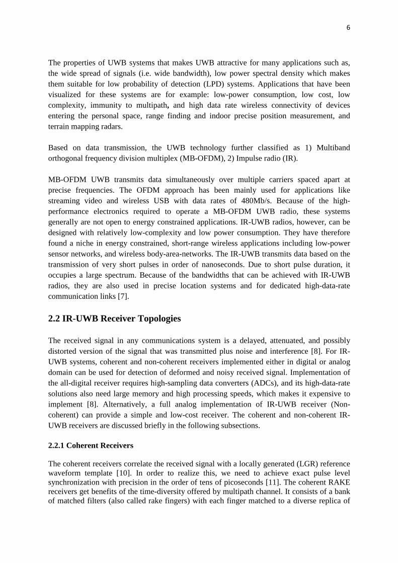
Table of contents Abstract …………………………………………………………….…………….…………...i Acknowledgement…………………………………………………………….………….….iii List of Tables………………………………………………………………..………………vii List of Figures……………………………………………………………………………......ix List of Acronyms…………………………………………………………………………….xi 1 Introduction 1.1 Background..………………………………………………………………………1 1.2 Research Goal ...…………………………………………………………………..2 1.3 Thesis organization …….…………………………………………………………3 2 Overview of UWB technology
2.1 UWB basics………………………………………………………………………..5 2.2 IR-UWB Receiver Topologies…………………………………………………….6 2.2.1 Coherent Receivers……...…………………………………………………..6
2.2.2 Non-coherent UWB receivers……………………………………………….7 2.2.2.1 Transmitted Reference Receivers………………………………………….7 2.2.2.2 Energy Detectors (ED)…………………………………………………….8 2.2.3 Comparison of coherent vs. non-coherent…………………………………...8 2.3 Simple IR-UWB working………………………………………………………….8 2.4 UWB Pulse Generation……………………………………………………………9 2.4.1 Gaussian monocycle………………………………………………………....9 2.4.2. Pulse shaping………………………………………………………………10 2.5 Pulse Modulation…………………………………………………………………12 2.5.1 Pulse Position Modulation (PPM)………………………………………….12 2.5.2 Bi-Phase Shift Keying (BPSK)…………………………………………….12
2.5.3 Pulse Amplitude Modulation (PAM)……………………………………....13 2.5.4 on/off keying (OOK)……………………………………………………….13
2.6 Access Methods…………………………………………………………………..14 2.7. Channel…………………………………………………………………………..14
3 Non-Coherent Energy Detector Receiver 3.1 Working Principle………………………………………………………………..15 3.2 Non idealities vs. performance discussion……………………………………….15 3.2.1. Noise Analysis……………………………………………………………..16 3.2.2 Noise figure………………………………………………………………..16 3.2.3 Nonlinear effects/Linearity………………………………………………...18 3.2.3.1 Inter-Modulation…………………………………………………..18
3.2.3.2 Linearity system level considerations……………………………..19 3.2.4 Need of LNA as first stage ………………………………………………..20

vi
3.3 LNA………………………………………………………………………………20 3.4 VGA……………………………………………………………………………...21 3.5 Square law device…………………………………………….…………………..21
4 Integrator 4.1Purpose……………………………………………………………………………23
4.2 Integrator performance metrics…………………………………………………..24 4.2.1 Ideal Integrator vs. Non-Ideal Integrator……………………………….. ..24 4.3 Integrator Modeling……………………………………………….……………...25
4.3.1 Integrator Modeling with Matlab……………………………………………25 4.3.1.1. Ideal Integrator…………………………………………………25
4.3.1.2. Non Ideal Integrator……………………………………………26 4.3.1.3. Non Ideal Integrator response for square wave………………...27
4.3.2 Integrator Modeling with Pspice…………………………………………..28 4.3.2.1 Inverting RC Op-amp integrator………………………………..29 4.3.2.1.2 Modified/Non-ideal integrator………………………………..29
4.3.2.2. Gm-C integrator………………………………………………..31 4.3.2.2.1 First order Non-ideal Gm-C integrator………………………..32 4.3.2.3. RC op-amp vs. Gm-C performance comparison in Pspice…….34
4.3.3 Integrator Optimization…………………………………………….……..35 4.3.3.1 Pspice to Matlab……………………………………………...…36
5 System level Simulations & Results 5.1 Introduction……………………………………………………………………....37 5.2 Performance Metrics……………………………………………………………..37 5.2.1 Link Budget………………………………………………………………...37 5.2.2 Bit Error Rate………………………………………………………………38
5.2.3 Threshold Decision Estimation…………………………………………….38 5.3System level implementation……………………………………………………..40 5.3.1 System level assumptions and system parameters………………………….40 5.3.2 Receiver system implementation without RF front-end non idealities…….41
5.3.2.1 Pulse generation…………………………………………………....42 5.3.2.2 Working…………………………………………………………….43 5.3.2.3 Performance evaluation…………………………………………….44
5.3.3 Receiver system implementation with RF front-end non idealities……..…44 5.3.3.1 The effect of LNA non idealities…...………………………………45 5.3.3.2 The effect of Squarer non idealities ..……………………………..46 5.3.3.3 Integrator Effect of Performance…………………………………...48
6 Summary and Future work…………………………………………..…………….51 Bibliography………………………………………………………………………...53 Appendix1 …………………………………………………………………………..56 Appendix 2…………………………………………………………………………..57

vii
List of Tables Table.2.1 Comparison of non-coherent and coherent receiver Table 3.1 Performance comparison with recent UWB LNA’s Table.5.1 Link Budget calculations Table.5.2 Different parameters and their values that are assumed during simulations Table.5.3 LNA Specifications comparison for low power wideband applications Table.5.4 Squarer Specifications from literature Table.5.5 Final building block specifications

viii

ix
List of Figures
Fig.1.1 Comparison of spread spectrum (SS), narrowband (NB), and (UWB) signal concepts Fig.2.1 UWB Mask as described by the FCC Fig.2.2 RAKE receiver Fig.2.3 Receiver for a standard TR-UWB communication system Fig.2.4 A non-coherent energy detector(ED) Receiver structure Fig.2.5 Block diagram of IR-UWB Communication System Fig.2.6 First derivative of a Gaussian pulse Fig.2.7 PSD of higher order derivatives of Gaussian pulse Fig.2.8 Gaussian Pulses (Amplitude vs. Time) examined in this work. Fig.2.9 PPM Waveform Fig.2.10 PPM Waveform Fig.2.11 OOK Waveform Fig.3.1 Non-coherent energy detector receiver structure Fig.3.2 Cascade chain of RF front end Fig.3.3 1dB compression point Fig. 3.4 a) Signal spectrum of nonlinear system, b) IIP3 Fig.3.5 Noise contribution during Mixer operation Fig.4.1 the block diagram of Squarer, Integrator and decision unit Fig.4.2 Magnitude and phase response of integrator Fig.4.3 LPF as Integrator Fig.4.4 Ideal integrator a) Step response b) Magnitude & phase response Fig.4.5 Non ideal integrator a) Bode plot & b) Step response Fig.4.6 Non ideal integrator with constant dc gain Fig.4.7 Integrator in Simulink and their transient response Fig.4.8 a) Square wave input b) LPF response instead of integrator Fig.4.9 Inverting RC op-amp integrator and its ac response Fig.4.10 Gm-C Integrator Fig.4.11Non ideal inverting RC op-amp Integrator in Pspice Fig.4.12Non ideal Gm-C op-amp Integrator in Pspice Fig.4.13Modified Gm-C filter response for Squarer unit output Fig. 5.1 BER vs. Threshold for estimating Threshold decision value Fig.5.2 Visualization of Threshold importance Fig.5.3 Block diagram of transceiver Fig 5.4 flowchart for the simulation of building blocks of energy detector transceiver Fig.5.5 UWB pulse and it’s PSD Fig.5.6 Energy detection operation with OOK modulation (1 pulse/bit) Fig.5.7 (a) performance analysis of receiver with out non idealities Fig.5.7 (b) flow chart to derive individual block specs Fig.5.8 LNA effect on BER Fig.5.9 Squarer Effect on BER Fig.5.10 Deviation in performance due to addition of non-ideal squarer from non-ideal LNA Fig.5.11 The effect of Integrator (variable dc gain, constant UGBW) Fig.5.12 Integrator Leakage effect on BER

x

xi
List of Acronyms
UWB Ultra Wideband RF Radio frequency SS Spread spectrum NB narrowband PAN Personal Area Networks BER Bit error rate ED Energy Detector FCC Federal Communications Commission, USA EIRP Effective Isotropic Radiated Power OFDM Orthogonal Frequency Division Multiplex ADC Analog to digital data converter LGR locally generated reference SNR signal to noise ratio MIMO Multiple-input and multiple output systems PSD power spectral density PPM Pulse Position Modulation BPSK binary phase shift keying ED Energy detection TR Transmitted reference LNA Low Noise Amplifier VGA Variable gain amplifier BPF Band pass filter NF noise figure IP3 Inter modulation product DR Dynamic range LPF Low pass filter TF Transfer function VCCS Voltage Controlled Current Source UGBW Unity gain bandwidth IL Implementation loss SNR Signal to noise ratio Eb/No The ratio of Energy per bit to noise power spectral density NBI Narrowband Interference

xii

1
Chapter-1 Introduction
1.1 Background Ultra wideband (UWB) technology emerged as a solution to meet the growing demands of short-range radio communication, low power RFID, wireless sensor networks and the internet of thing’s applications, with requirements like, high speed, high data rates(in order of few hundred Mbps), precise positioning capability, etc. UWB differs significantly from conventional narrow band radio frequency (RF) and spread spectrum technologies (SS), such as Bluetooth Technology and 802.11a/b/g, GSM, etc. UWB uses a very large wide band of RF spectrum to transmit data as in Fig.1.1. Hence, UWB can transmit more data in a given period of time than usual radios [2].
Fig.1.1 Comparison of spread spectrum (SS), narrowband (NB), and (UWB) signal concepts The absence of carrier frequency is the other fundamental attribute that differentiates impulse radio based ultra wideband (IR-UWB) from narrow-band applications. In place of broadcasting on separate frequencies like narrow band applications, UWB spread’s signals across a very broad range of frequencies. Due to wide bandwidth and stringent low power transmission limits, the UWB transmissions appear as background noise to nearby traditional radios. The initiative of using ultra short impulses for communication was first presented in the work [3]. Though UWB is the not new concept, it was in use for radar, sensing, military communications and other niche applications in the last three decades. Only after FCC issued a ruling in 2002 stating that the unlicensed 3.5 GHz to 10.6 GHz band (UWB) with the stringent power limits of -41.3dBm/MHz can be used for data communications, consumer electronics and safety applications. Then the UWB technology received significant interest in both academia and industry due to its research & market potential. UWB technology offers several advantages over narrowband communication systems due to huge bandwidth and short pulse duration. The main advantages of the UWB communication system include such as,
UWB
NB
SS
Ener
gy o
utpu
t
Frequency Range

2
(i) High Channel Capacity and High Data Rates: The large bandwidth occupied by UWB gives the potential of very high channel capacity, yielding excessive data rates. From Shannon’s formula,
𝐶 = 𝐵 log2 1 + SN (eq.1.1)
Where: C: Channel capacity (bps); B: Channel bandwidth (Hz); S: Signal Power; N: Noise power(W) Channel capacity is directly proportional to signal bandwidth. Due to large bandwidth, UWB has a huge potential for high-speed wireless communications.
(ii) Low Power Consumption: Due to strict UWB mask limits, UWB devices operate under very low power. With appropriate engineering design, the resulting power consumption of UWB can be pretty low. As with technology, the power consumption is expected to decrease as circuits are designed with more efficiency, and more signal processing is done on smaller chips at lower operating voltages [1]. The current target for power consumption of UWB chip sets is less than 100mW. (iii) Immune to Interference: Due to small PSD, UWB signals cause very little interference with existing narrow band radio systems. Impulse signals have low susceptibility to multipath interference in transmitting information in the UWB communication system because the transmission duration of a UWB pulse is shorter than a nanosecond in most cases. Even it gives rise to a fine resolution of reflected pulses at the receiver. Therefore, UWB communication system can resolve the fading problem. (iv) High Security: While UWB systems work under noise floor, they are naturally hidden and extremely difficult for unauthorized users to detect. (v) High precision ranging: Due to fine time resolution of IR-UWB, it can be used for precise positioning and location tracking applications. (vi) Low complexity and Low Cost: Emission of low powered pulses by the transmitter eliminates the need of power amplifier and because UWB transmission is a carrier less, there is no need for mixers and local oscillators to translate carrier frequency to a required frequency band. Hence, it avoids the need for a carrier recovery stage at the receiver end. The lack of a carrier may be traded for a low-power solution unlike it doesn’t waste power on a carrier in narrow band applications. There is also demand for short-range low data rate communication links in wearable and implantable microelectronics and wireless sensor networks [4] [5]. In several of these applications, like implantable devices, ultra-low power is important. Exploring impulse radio for robust wireless communication in medical applications is also interesting. Applications like positioning, locating, penetrating through walls, wireless Ad-Hoc Networks, tracking objects, etc. make this feature unique. As a result UWB technology research has been shifted to consumer electronics and communications applications. 1.2 Research Goal Though a lot of research carried out on UWB technology to make it, more robust, reliable and flexible wireless communication, still there are few challenges yet to be examined carefully

3
to ensure the success of UWB technology. The main challenges that still require extensive research include: optimum transceiver design, impact of non-idealities on the performance, interference cancellation, time synchronization for short-duration pulses, accurate channel modeling, and leakage behavior of integrator for energy detector (ED) receivers. This thesis mainly focuses on system-level modeling of a non-coherent IR-UWB energy detector receiver for low power, medium data rate (few hundred Mbps) applications. During the processing of the received signal, it is subjected to various impairments/non idealities of each front end blocks, which will affect the overall performance of the receiver. It is very crucial to understand trade off among different parameters of front end components and thus relax design requirements, complexity from circuit point of view. The main objectives of the thesis are listed as below
• The system level modeling of non-coherent IR-UWB energy detector receiver. • Study the effect of non-idealities (NF, IP3, and Gain) of each front end RF block on
the performance is investigated. • Analyze the leakage behavior of Integrator, a base band block. • Study the effect of leakage of baseband block (Integrator) on the overall performance
of the receiver.
1.3 Thesis organization The thesis is organized as follows, Chapter 2: Present’s basics of UWB technology, overview of UWB-IR receiver topologies, different modulation techniques, pulse shaping and short discussion about access methods and channel. Chapter 3: It gives brief explanation about architecture of IR-UWB ED receiver, and its operation in detail followed by noise analysis and linearity analysis. Then RF front end blocks LNA and Squarer are considered in more detail. Chapter 4: This chapter provides investigation on integrator leakage behavior including leakage effect on performance. Integrator was modeled in Matlab from a filter prospective. Then RC op-amp and Gm-C integrator was investigated in detail from Pspice, and it also provides how different parameters of integrator like GBW, DC gain and leakage affect the receiver performance. Chapter 5: This chapter provides radio essentials to understand performance evaluation and system level implementation using Matlab and the effect of non-idealities of each RF front-end blocks on the receiver performance are investigated, and results are discussed in detail. Chapter 6: This chapter provides discussion on summary and future work.

4

5
Chapter 2 Overview of UWB technology
2.1 UWB Basics UWB considered as one of the most exciting technologies in the wireless world today due to its capability of transmitting data over a wide frequency spectrum for short distances with very low power and high data rates. According to FCC, UWB signals are defined as signals, which have a fractional bandwidth greater than 20% of the center frequency measured at -10dB points and occupy minimum band width of 500MHz. Here, fractional bandwidth is defined as 2(FH – FL)/ (FH + FL) and the center frequency (FH + F L)/2.Where FH and FL are upper and lower frequency limits [6]. In order to regulate UWB systems, FCC has allocated unlicensed frequency spectrum from 3.1GHz to 10.6GHz, with very strict effective isotropic radiated power (EIRP) limits to be -41.3dBm/MHz for UWB systems. Fig.2.1 shows the masks for data communication applications for indoor and outdoor use as per FCC [20].
Figure 2.1 UWB Mask as described by the FCC [6] From theoretical point of view, Shannon’s theorem provides why UWB is very attractive to meet modern day communication needs. Shannon’s theorem relates the capacity of a system with its bandwidth and signal to noise ratio. It is expressed as: 𝐶 = 𝐵 log2 1 + S
N (eq.2.1)
Where: C: Channel capacity (bps); B: channel Bandwidth(Hz); S: signal power and N: Noise power(W) From the eq.2.1 it is obvious that the capacity of a communication system raise quicker as the function of the channel bandwidth than in terms of the power [9]. However, conventional wireless communication systems emerged using narrowband systems that are limited by power and bandwidth. Therefore, they have a limited channel capacity. Alternatively, the increasing need of high data rates in wireless communication applications will entail the use of wideband systems capable of handle from few GHz to several GHz in order to meet the future demands. Thus, UWB technology appears as a solution for high data rate applications.
Frequency [GHz]
UW
B EI
RP E
miss
ion
leve
l [dB
m/M
Hz]
6
The properties of UWB systems that makes UWB attractive for many applications such as, the wide spread of signals (i.e. wide bandwidth), low power spectral density which makes them suitable for low probability of detection (LPD) systems. Applications that have been visualized for these systems are for example: low-power consumption, low cost, low complexity, immunity to multipath, and high data rate wireless connectivity of devices entering the personal space, range finding and indoor precise position measurement, and terrain mapping radars. Based on data transmission, the UWB technology further classified as 1) Multiband orthogonal frequency division multiplex (MB-OFDM), 2) Impulse radio (IR). MB-OFDM UWB transmits data simultaneously over multiple carriers spaced apart at precise frequencies. The OFDM approach has been mainly used for applications like streaming video and wireless USB with data rates of 480Mb/s. Because of the high-performance electronics required to operate a MB-OFDM UWB radio, these systems generally are not open to energy constrained applications. IR-UWB radios, however, can be designed with relatively low-complexity and low power consumption. They have therefore found a niche in energy constrained, short-range wireless applications including low-power sensor networks, and wireless body-area-networks. The IR-UWB transmits data based on the transmission of very short pulses in order of nanoseconds. Due to short pulse duration, it occupies a large spectrum. Because of the bandwidths that can be achieved with IR-UWB radios, they are also used in precise location systems and for dedicated high-data-rate communication links [7]. 2.2 IR-UWB Receiver Topologies The received signal in any communications system is a delayed, attenuated, and possibly distorted version of the signal that was transmitted plus noise and interference [8]. For IR-UWB systems, coherent and non-coherent receivers implemented either in digital or analog domain can be used for detection of deformed and noisy received signal. Implementation of the all-digital receiver requires high-sampling data converters (ADCs), and its high-data-rate solutions also need large memory and high processing speeds, which makes it expensive to implement [8]. Alternatively, a full analog implementation of IR-UWB receiver (Non-coherent) can provide a simple and low-cost receiver. The coherent and non-coherent IR-UWB receivers are discussed briefly in the following subsections. 2.2.1 Coherent Receivers
The coherent receivers correlate the received signal with a locally generated (LGR) reference waveform template [10]. In order to realize this, we need to achieve exact pulse level synchronization with precision in the order of tens of picoseconds [11]. The coherent RAKE receivers get benefits of the time-diversity offered by multipath channel. It consists of a bank of matched filters (also called rake fingers) with each finger matched to a diverse replica of

7
the same transmitted signal, see Fig.2.2. The outputs of the fingers are appropriately weighted and added to harvest the advantages of multipath diversity. As the number of fingers increases the complexity will be increased. In spite of its complexity in architecture, it finds various UWB applications e.g. Multiple-input and multiple output systems (MIMO) [12], BAN, etc. The coherent RAKE receivers have to cope with greater design challenges like very accurate pulse level synchronization to correlate received signal with template signal. Precise template signal design is required to maximize the signal to noise ratio (SNR). Finally, multipath energy combining requires a RAKE matched-filter receiver with more fingers, which leads to high complexity of receiver design.
Fig.2.2. RAKE receiver [13]
2.2.2 Non-coherent UWB receivers Non-coherent UWB receivers such as the energy detector and the autocorrelation receivers are promising alternatives to coherent receivers. Non-coherent receivers do not have need of phase of channel, and have less complexity for implementation. The non-coherent receivers, particularly suitable for low power and low-cost applications such as personnel area network and wireless sensor networks [19]. Two popular non-coherent detection schemes for IR-UWB signals are transmitted reference (TR) receiver and energy detectors (ED). 2.2.2.1 Transmitted Reference Receivers The non-coherent transmitted reference receiver shown in Fig.2.3 demodulates the signals transmitted by TR modulation [14]. The reference signal delayed by D units in the TR receiver and correlates it with data-modulated signal in each frame. A threshold decision is made on to integration over all acquired frames during a symbol period. TR receivers exploit multipath diversity inherent in the environment without the need for stringent acquisition and channel estimation [13]. On the other hand, TR receiver provides relatively poor bit error rate and low data rates.
Fig.2.3. Receiver for a standard TR-UWB communication system [14]
Matched filter 1
Matched filter 2
Matched filter k
Path searcher
Correlator
Recovered Signal Received Signal
Synchronization Sequence
LPF 𝑇𝑠
0
D
X r r(t)
(t)
8
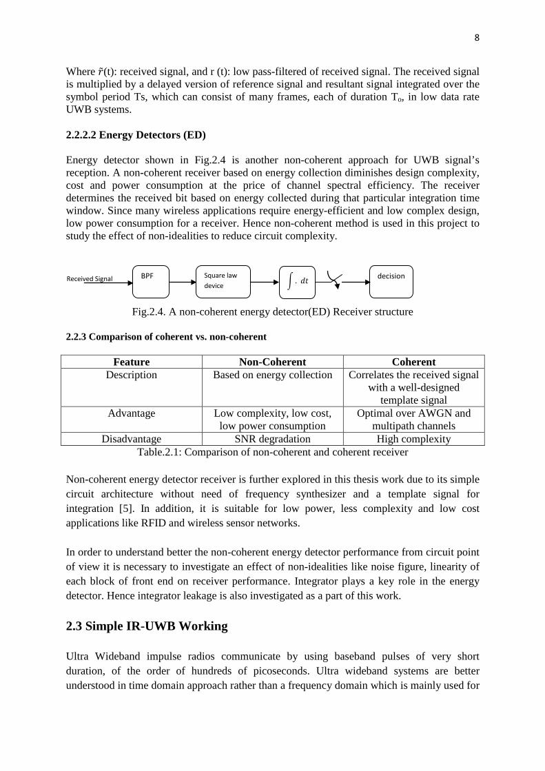
Where (t): received signal, and r (t): low pass-filtered of received signal. The received signal is multiplied by a delayed version of reference signal and resultant signal integrated over the symbol period Ts, which can consist of many frames, each of duration To, in low data rate UWB systems. 2.2.2.2 Energy Detectors (ED) Energy detector shown in Fig.2.4 is another non-coherent approach for UWB signal’s reception. A non-coherent receiver based on energy collection diminishes design complexity, cost and power consumption at the price of channel spectral efficiency. The receiver determines the received bit based on energy collected during that particular integration time window. Since many wireless applications require energy-efficient and low complex design, low power consumption for a receiver. Hence non-coherent method is used in this project to study the effect of non-idealities to reduce circuit complexity.
Fig.2.4. A non-coherent energy detector(ED) Receiver structure 2.2.3 Comparison of coherent vs. non-coherent
Feature Non-Coherent Coherent Description Based on energy collection Correlates the received signal
with a well-designed template signal
Advantage Low complexity, low cost, low power consumption
Optimal over AWGN and multipath channels
Disadvantage SNR degradation High complexity Table.2.1: Comparison of non-coherent and coherent receiver
Non-coherent energy detector receiver is further explored in this thesis work due to its simple circuit architecture without need of frequency synthesizer and a template signal for integration [5]. In addition, it is suitable for low power, less complexity and low cost applications like RFID and wireless sensor networks. In order to understand better the non-coherent energy detector performance from circuit point of view it is necessary to investigate an effect of non-idealities like noise figure, linearity of each block of front end on receiver performance. Integrator plays a key role in the energy detector. Hence integrator leakage is also investigated as a part of this work. 2.3 Simple IR-UWB Working Ultra Wideband impulse radios communicate by using baseband pulses of very short duration, of the order of hundreds of picoseconds. Ultra wideband systems are better understood in time domain approach rather than a frequency domain which is mainly used for
BPF Square law device . 𝑑𝑡 decision Received Signal
9
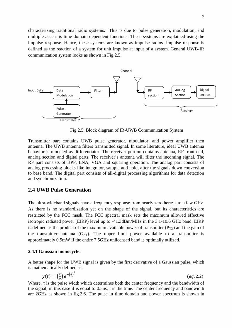
characterizing traditional radio systems. This is due to pulse generation, modulation, and multiple access is time domain dependent functions. These systems are explained using the impulse response. Hence, these systems are known as impulse radios. Impulse response is defined as the reaction of a system for unit impulse at input of a system. General UWB-IR communication system looks as shown in Fig.2.5.
Channel
Input Data Receiver Transmitter
Fig.2.5. Block diagram of IR-UWB Communication System
Transmitter part contains UWB pulse generator, modulator, and power amplifier then antenna. The UWB antenna filters transmitted signal. In some literature, ideal UWB antenna behavior is modeled as differentiator. The receiver portion contains antenna, RF front end, analog section and digital parts. The receiver’s antenna will filter the incoming signal. The RF part consists of BPF, LNA, VGA and squaring operation. The analog part consists of analog processing blocks like integrator, sample and hold, after the signals down conversion to base band. The digital part consists of all-digital processing algorithms for data detection and synchronization. 2.4 UWB Pulse Generation The ultra-wideband signals have a frequency response from nearly zero hertz’s to a few GHz. As there is no standardization yet on the shape of the signal, but its characteristics are restricted by the FCC mask. The FCC spectral mask sets the maximum allowed effective isotropic radiated power (EIRP) level up to -41.3dBm/MHz in the 3.1-10.6 GHz band. EIRP is defined as the product of the maximum available power of transmitter (PTX) and the gain of the transmitter antenna (GAT). The upper limit power available to a transmitter is approximately 0.5mW if the entire 7.5GHz unlicensed band is optimally utilized. 2.4.1 Gaussian monocycle: A better shape for the UWB signal is given by the first derivative of a Gaussian pulse, which is mathematically defined as:
𝑦(𝑡) = 𝑡𝜏 𝑒−
𝑡𝜏2
(𝑒𝑞. 2.2) Where, τ is the pulse width which determines both the center frequency and the bandwidth of the signal, in this case it is equal to 0.5ns, t is the time. The center frequency and bandwidth are 2GHz as shown in fig.2.6. The pulse in time domain and power spectrum is shown in
Data Modulation
Pulse Generator
Filter RF section
Digital section
Analog Section

10
fig.2.6. This pulse forms part of a group of Gaussian pulses called mono cycles whose main characteristic is that they do not contain low-frequency components including DC. As a result, this facilitates the design of the other components such as antennas, amplifiers and sampling down converters.
Fig.2.6. First derivative of a Gaussian pulse [16]
2.4.2. Pulse shaping The aim of UWB pulse shape design is to obtain a pulse waveform that meets FCC spectral mask requirements and also to maximize the bandwidth. The pulse shape plays a crucial role since it directly affects power spectral density (PSD) of transmitted signal [17]. The spectrum can be shaped by varying pulse width, pulse derivative and combination of base functions. In general higher derivatives of Gaussian pulses are more popular for UWB transmission. This is due to the DC value of Gaussian pulse and inefficiency of antennas at DC. The number of zero crossings increases as Gaussian pulse derivative order increases with the same pulse width. The center frequency will increase and band width decrease as we go higher derivative of Gaussian pulse.

11
Fig.2.7. PSD of higher order derivatives of Gaussian pulse [18]
In the thesis work Gaussian monocycle, Gaussian doublet and Gaussian 5th derivative are examined and shown in Fig.2.8
(a) Gaussian First order (b)Gaussian doublet
(c) Gaussian Fifth derivative (d) PSD of 1st, 2nd, 5th Gaussian derivatives
Fig.2.8. Gaussian Pulses (Amplitude vs. Time) examined in this work.
-3 -2 -1 0 1 2 3
x 10-9
-1
-0.5
0
0.5
1y1
-3 -2 -1 0 1 2 3
x 10-9
-0.5
0
0.5
1y2
-3 -2 -1 0 1 2 3
x 10-9
-1
-0.8
-0.6
-0.4
-0.2
0
0.2
0.4
0.6
0.8
1y5
0 5 10 15 20-90
-80
-70
-60
-50
-40
Frequency (GHz)
PS
D (d
Bm
)
1st,2nd,5th derivative of gaussian pulse(PSD) compared with FCC mask
1st derivative2nd derivative5th derivative
center frequency increase as we move to higher derivative
FCC Mask
Time (s) Time (s)
Amp
Amp
Amp

12
From the above examination, Gaussian 5th derivative is considered with center frequency at 4GHz which best suits lower UWB band under examination for energy detector. The power spectrum density of Gaussian pulse train is as shown below in fig 2.8.d. Here, spikes indicate that each pulse repeats after pulse repetition frequency of 333MHz.
Fig.2.8.d PSD of Gaussian pulse train
2.5 Pulse Modulation The modulation techniques available for UWB communications principally classified as shape-based (binary phase shift keying (BPSK), pulse amplitude modulation (PAM), On/Off keying (OOK), orthogonal pulse modulation (OPM)) and time based (pulse position modulation (PPM)). 2.5.1 Pulse Position Modulation (PPM) In PPM modulation, the binary bit to be transmitted affects the position of the UWB pulse. The bit ‘0’ is represented by a pulse originating at same time instant 0, but the bit ‘1’ is shifted in time by the amount of δ from 0. Modulated data can be represented mathematically by, 𝑌(𝑡) = ∑ 𝑊𝑡𝑟
𝑗=∞𝑗=−∞ 𝑡 − 𝑗𝑇 − 𝛿 × 𝑑𝑗 (𝑒𝑞. 2.3)
Where𝑊𝑡𝑟: pulse waveform, T: bit duration, δ: fixed delay, dj: binary data
Fig.2.9. PPM Waveform
2.5.2 Bi-Phase Shift Keying (BPSK) BPSK is also called as antipodal modulation and in this method the polarity of transmitted pulses will change according to binary data as shown in below fig.2.9. It can be represented mathematically as,
𝑌(𝑡) = 𝑊(𝑡 − 𝑗𝑇)2𝑑𝑗 − 1𝑗=∞
𝑗=−∞
(𝑒𝑞. 2.4)
0 2 4 6 8 10-450
-400
-350
-300
-250
-200
-150
-100
-50
0
Frequency (GHZ)
PSD d
Bm/M
hz
PSD of Pulse train
FCC Mask

13
Where W: pulse waveform, T: bit duration, dj: binary data
Fig.2.10. PPM Waveform
2.5.3 Pulse Amplitude Modulation (PAM) The binary pulse amplitude modulation can be presented using two antipodal Gaussian pulses. The transmitted binary base band pulse amplitude modulated information signal can be represented as, 𝑥(𝑡) = 𝑑𝑗 ∗ 𝑤𝑡𝑟(𝑡) (𝑒𝑞. 2.5) Where wtr(t) is UWB pulse waveform and j is binary data ‘0’ or ‘1’.
dj=−1, 𝐽 = 01, 𝐽 = 1
2.5.4 On/Off keying (OOK) OOK modulation is much similar to PAM except that there is no data transmission while binary data to be transmitted is ‘0’. The transmitted binary OOK modulated information signal can be represented as
𝑥(𝑡) = 𝑑𝑗 ∗ 𝑤𝑡𝑟(𝑡) Where wtr(t) is UWB pulse waveform and j is binary data ‘0’ or ‘1’.
dj=0, 𝐽 = 01, 𝐽 = 1
Fig.2.11. OOK Waveform
In the above figure one bit represented by one pulse with pulse duration of 3ns. The big obscurity of OOK is in the existence of multipath, in which echoes of the native or other pulses make it tough to verify the absence of a pulse. Comparison of various modulation methods [1]: Modulation Method Advantages Disadvantages PPM Simplicity Needs fine time resolution BPM Simplicity, efficiency Binary only PAM Simplicity Noise immunity OOK Simplicity Binary only, Noise immunity
0 2 4 6 8 10 12 14 16 18-1
-0.5
0
0.5
1
Time (ns)
Am
plitu
de (v
)
OOK Modulation
01 1 10 0

14
OOK modulation is chosen for this work because it has information on signal amplitude, no need to bother about the phase, implementation has low complexity and low power consumption. 2.6 Access Methods Direct sequence (DS-UWB) and Time hopping (TH-UWB) are two spread-spectrum multiple access techniques that have been in use with UWB impulse radios. Both techniques use pseudo-random codes to separate different users. These spectrum randomization techniques are used to limit the interference caused by the transmitted UWB pulse train to existing low power narrow band radios like zigbee, wifi, etc. OOK can’t take advantage of Time hopping spreading because of no transmission in case of bit ‘0’, and it add further synchronization problems. 2.7. Channel: Channel is propagation environment that a signal passes through from transmitter to receiver. UWB channel model is extremely multipath rich compared to wideband channel. Detailed characterization of UWB radio propagation is one of the major requirements for successful design of UWB communication systems. However, the comprehensive channel modeling is out of scope of this work. Hence channel is modeled as an additive white Gaussian noise (AWGN) channel. As a result, this AWGN channel adds only white noise with constant spectral density and Gaussian distribution of amplitude to transmitted signal. It is further assumed that channel is free from multipath components, fading, interference and dispersion.
Rx_signal=Tx_signal+channel_noise (eq.2.6)

15
Chapter 3 Non-Coherent Energy Detector Receiver
This chapter describes the operation of non-coherent energy detector and functional blocks involved in detail. First investigation is carried out on noise analysis followed by linearity analysis. Then this chapter gives a brief discussion about each building block. 3.1 Working Principle The signal flow in non-coherent energy detector is as shown in Fig.3.1.
Fig.3.1. Non-coherent energy detector receiver structure
The wide-band pass filter (BPF) filters the received weak signal to remove the interfering signals from nearby narrowband devices. The first amplification of filtered received weak signal is done by low noise amplifier (LNA) and additional amplification made by variable gain amplifier (VGA) to improve the quality of signal as needed for further processing. The amplification value must be high enough to advance the process of the weak received signals. Then square law device down convert’s amplified signal from RF to desired base band frequencies. Then integrator collects energy of base band signal over desired band width. Then sample and hold unit will hold the value. After this, energy detector/comparator converts received pulse energy to binary ‘1’ or ‘0’ based on threshold energy value. Then performance of the receiver analyzed in terms of bit error rate.
3.2 Non idealities vs. Performance In RF system, signals are processed by cascaded stages as shown in Fig.3.1.The performance of RF system depends on various factors such as channel characteristics, interferences from surrounding radios, and internally by circuit non ideal effects, etc., RF front-end is the first element in the reception chain and is one of the most critical parts. The RF front end non-idealities limit the overall performance. Hence, it is important to know how the nonlinearity of each stage affects the performance. In this thesis, the effects of circuit non-idealities on receiver performance are investigated with the help of system-level simulations.

16
This study helps to relax requirements on front end blocks from circuit point of view, and it also helps in designing optimal RF system. In the UWB context, it is essential to study the effect of block level non-idealities on the overall receiver chain since received signals are often weak in orders of -79 dBm [21]. In order to receive such a weak signal, UWB receiver must have very good sensitivity. The receiver sensitivity is often limited by the receiver noise figure and overall distortion is best captured by the input referred third order inter-modulation product (IIP3) parameter. In addition to these non-idealities, the integrator leakage also plays a greater role in deciding performance of a non-coherent energy detector. The non-idealities NF, IIP3 at block level and integrator leakage is further explored in detail in the next sections. 3.2.1. Noise Analysis Noise analysis plays an important role in selecting high level specifications of an RF receiver such as sensitivity. Noise in an RF circuit affects directly high level system performance like SNR, BER whereas noise is second order effect in digital circuits. Noise is any undesired signal that interferes with desired signals being processed or unwanted signal generated by a device itself. There are several forms of electrical noise in electronic circuits including thermal noise and shot noise. The Noise power of received signal at the input depends on various factors. Assuming thermal noise, which is innate, is the only noise present at the input and no interference signals in UWB. Thermal noise occurs due to random thermal motion of charge carriers in conductors which is independent of applied voltage across the conductor. Thermal noise across resistor R can be modeled as series noise voltage generator 𝑉𝑛𝑜𝑖𝑠𝑒2 .
𝑉𝑛𝑜𝑖𝑠𝑒2 = 4𝐾𝑇𝑅𝐵 Where K: Boltzmann’s constant=1.38e-23 m^2 kg/s^2 K
B: Band width; T: Absolute temperature (Kelvin) This noise is further degraded as it passes through preceding stages of the receiver chain. As a result, the signal strength degrades as it passes through each stage. The amount of degradations of noise contributed by each stage of RF front end is quantified by a parameter called noise figure. 3.2.2 Noise Figure defined as a ratio of SNR at input to SNR at output. In other words, noise figure is a measure of how much the signal SNR degrades as it passes through each stage.
𝑁𝑜𝑖𝑠𝑒 𝐹𝑖𝑔𝑢𝑟𝑒 =𝑆𝑁𝑅𝑖𝑛𝑆𝑁𝑅𝑜𝑢𝑡
𝑃𝑠𝑖𝑔 = 𝑃𝑅𝑆 ⋅ 𝑁𝐹 ⋅ 𝑆𝑁𝑅𝑜𝑢𝑡 Where Psig denotes input signal power, PRS source resistance noise power, both per unit BW.
𝑃𝑠𝑖𝑔,𝑡𝑜𝑡 = 𝑃𝑅𝑆 ⋅ 𝑁𝐹 ⋅ 𝑆𝑁𝑅𝑜𝑢𝑡 ⋅ 𝐵 Where Psig,tot is the overall signal power distributed across the channel bandwidth B. In other words, it is known as sensitivity. The radio sensitivity can be defined as the minimum detectable signal (MDS) level at the antenna with acceptable signal to noise ratio. The receiver sensitivity expressed in dBm as Pin,min |dBm = PRS|dBm/Hz + 𝑁𝐹|dB + 10 log𝐵 + 𝑆𝑁𝑅min|dB (𝑒𝑞 3.1)

17
Where Pin,min: minimum received signal level that achieves SNRmin, SNRmin: minimum acceptable SNR at receiver output, which is function of
Minimum required BER at the output of demodulator. B: bandwidth in Hz, PRS: source noise power: -174dBm/Hz;
The first three terms on right side of above equation (eq3.1) represents noise floor. The thermal noise referred to the input of radio system is also called noise floor. Consequently, the noise power which appears at the receiver input is determined by the voltage divider between the receiver input resistance (𝑅𝑖𝑛) and the antenna source resistance (𝑅𝑠).
𝑃𝑛𝑜𝑖𝑠𝑒 =𝑉𝑖𝑛2
𝑅𝑖𝑛=
𝑅𝑖𝑛𝑅𝑠(𝑅𝑖𝑛 + 𝑅𝑠)2
4𝑘𝑇𝐵𝑤
Most receivers designed for maximum power transfer from the antenna to the input of the receiver, in which case, 𝑅𝑠 = 𝑅𝑖𝑛 = 𝑅 above equation becomes
𝑃𝑛𝑜𝑖𝑠𝑒 = 𝑘𝑇𝐵𝑤 In RF circuit design, power levels are commonly referred to in decibels referenced to 1mW (or) 0dBm. At 300 K, the noise power in dBm for target channel bandwidth from 3GHz to 5GHz is
𝑃𝑛𝑜𝑖𝑠𝑒,𝑑𝐵𝑚 = 10 ∗ 𝑙𝑜𝑔10 1.38𝑒 − 23 ∗ 290 ∗1𝑒3𝑚𝑊𝑊
+ 10 ∗ log10(BW)
=−174 + 10 log10 2𝑒9 = −81𝑑𝐵𝑚 The 𝑒𝑞 3.1 can be rewritten as
𝑆𝑁𝑅𝑖𝑛,𝑑𝐵𝑚 = 𝑃𝑚𝑑𝑠,𝑑𝐵𝑚 − 𝑁𝐹 − 𝑃𝑛𝑜𝑖𝑠𝑒,𝑑𝐵𝑚 From this equation, clearly that NF affects the receiver sensitivity since SNRin is dependent on tolerable bit error rate of target application. 3.2.2.1 NF System level consideration The received signal by antenna propagates through different blocks before it reaches digital back-end in the receiver path. During this process, each block introduces noise to the signal characterized by noise figure. The overall noise figure of the receiver depends on the noise contributed by each block as well as the gain of preceding stages. Naturally, larger signals are less prone to noise, and this is why large gain of one stage makes the noise contributed by next stage is less important. Finally, from Friis’ equation [22], overall NF of the cascade system shown in Fig.3.2 which is given by 𝑒𝑞 3.2
Fig.3.2. Cascade chain of RF front end
𝑁𝐹𝑟𝑥 = 𝑁𝐹1 +𝑁𝐹2𝐺1
+𝑁𝐹3𝐺1𝐺2
+ ⋯ (𝑒𝑞. 3.2)
NF1 G1
NF2 G2
NF3 G3

18
Where NFi and Gi are the NF and available power gain of i-th stage respectively. Assuming that G1 is a larger value then NF1 is the dominant term in the above equation. From this it is clear that first stage dominates overall NF of the receiver. From this 𝑒𝑞. 3.2, it is very clear that first stage is the most important noise contributor to overall noise of the receiver. Since, it adds up directly. Hence, it is important to keep the noise figure of first stage as low as possible. Extra care has to be taken while determining specifications of first stage. This leads to stringent requirements like low NF and high gain on first stage, which usually LNA. NF2 is the NF of second stage, which usually a self-mixer in an energy detector. Mixing operation is usually noisier. Hence Self mixer usually shows much higher NF than LNA. Therefore, gain of LNA must be large enough to reduce the noise contribution by next stages. 3.2.3 Nonlinear effects/Linearity
Linearity sets dynamic range (DR) of the receiver. Dynamic range is the ratio of the maximum input signal that the circuit can tolerate to minimum input signal that can provide adequate signal quality. The upper limit of dynamic range in high-frequency applications is limited by inter-modulation distortion or 1dB compression. Whereas at low-frequency applications, most input power circuit can tolerate without saturation. The input third order intercept point (IIP3) and 1-dB compression point is used for the measure of linearity in UWB applications. One dB compression point defined as the input signal level that causes the small-signal gain to drop by 1dB below its nominal value as shown in Fig.3.3.
Fig.3.3 1dB compression point
Input signals above compression point are usually saturated at output. Hence, 1dB compression point considered as upper bound on dynamic range. 3.2.3.1 Inter-Modulation Inter-modulation products caused due to multiplication (mixing) of input signal with its harmonics due to nonlinear nature of real systems. When two signals with different frequencies applied to a nonlinear system, the output in general exhibits some components which are not a harmonic of input frequencies. The frequency of these unwanted components may be very close to that of desired signals resulting in signal distortion. This can be demonstrated briefly by assuming the nonlinear system with input and output related by, 𝑌(𝑡) = 𝛼1𝑥(𝑡) + 𝛼2𝑥(𝑡)2 + 𝛼3𝑥(𝑡)3 + ⋯ (𝑒𝑞. 3.3)
Let substitute x(t)=A(cos(w1t)+cos(w2t)) in (eq3.3)

19
Then the following terms exist in the vicinity of w1 and w2.
First order terms:𝑎𝑡 𝑤1:𝑦𝑤1 = (𝛼1𝐴 + 9
4𝛼3𝐴3)cos (𝑤1𝑡)
𝑎𝑡 𝑤2:𝑦𝑤2 = (𝛼1𝐴 + 94𝛼3𝐴3)cos (𝑤2𝑡)
(𝑒𝑞. 3.4)
Third order IMP terms:𝑎𝑡 2𝑤1 − 𝑤2:𝑦2𝑤1−𝑤2 = 3
4𝛼3𝐴3cos (2𝑤1 − 𝑤2)𝑡
𝑎𝑡 2𝑤2 − 𝑤1:𝑦2𝑤2−𝑤1 = 34𝛼3𝐴3cos (2𝑤2 − 𝑤1)𝑡
(𝑒𝑞. 3.5)
Fig. 3.4 a)Signal spectrum of the nonlinear system b) IIP3
In general, α3 is negative number and is much smaller than α1, so for small input signals the first-order terms are dominant at the output. As amplitude of input increases, the first-order component increases directly proportional to A (amplitude), where as a third-order inter modulation product increase in proportion to A3. The input level for which first order term and output inter modulation product have same power is identified as third order intercept point (IIP3).
Input IP3 𝐴𝐼𝑃3 = 43𝛼1α3
The above calculations are based on the assumption that terms (9/4 α3A3) are negligible in the yw1 and yw2. These assumptions are no longer valid for larger amplitude signals hence calculated value of IIP3 is equal to extrapolation of the small input behavior of the system as shown in Fig.3.4 b. 3.2.3.2 Linearity system level considerations The receiver performance is also affected by linearity of each individual block. This can be shown analytically by eq.3.6 for cascading chain Fig.3.2. The worst case IIP3 (A2
IIP3,tot) of the receiver system in terms of the IIP3 of each individual block in the cascade chain given by 1
𝐴𝐼𝐼𝑃3,𝑡𝑜𝑡2 ≈ 1
𝐴𝐼𝐼𝑃3,12 + 𝐺𝐼
2
𝐴𝐼𝐼𝑃3,22 + 𝐺𝐼
2𝐺22
𝐴𝐼𝐼𝑃3,32 + ⋯ (𝑒𝑞 3.6)
Where AIIP3,i and Gi are the IIP3 and gain of the ith stage, respectively. From careful observation of above equation, it is clear that if each stage in cascade has a gain greater than unity, then the nonlinearity of following stage becomes more critical. This means that the nonlinearity of first building block of the receiver, doesn’t affect overall nonlinearity as much as nonlinearity of the next stages, e.g. self-mixer does. From above expression it also implies that high gain of first stage degrades the overall linearity of the system.

20
It is in contrast with NF scenario where the high gain of first stage improves overall NF. Despite the opposing behaviors of NF and linearity, designers typically try to maximize the gain of first stage to meet better noise figure response as UWB signals are weak in nature.
3.2.4 Need of LNA as the first stage block The power of received signal is also calculated from 𝑃𝑟𝑥 = 𝑃𝑡𝑟 + 𝐺𝑡 + 𝐺𝑟 − 𝑃𝑙𝑜𝑠𝑠 (𝑒𝑞. 3.7) Where Prx: Available power of received signal (dBm) Ptr: power of transmitted signal (dBm) Gt: Transmission antenna gain (dB) Gr: Receiver antenna gain (dB) Ploss: power of path loss dependent on distance between transmitter and receiver (dB) Since UWB systems use spread spectrum techniques to avoid interferences to nearby radios by distributing power across the entire bandwidth. Hence, they have been processing gain. The processing gain is defined as a relation of spread bandwidth to bandwidth of the information signal at receiver output. 𝑃𝐺 = 10 log10(𝐵/𝑟) Where B: bandwidth; r: bit rate of system PG is also one of the parameters that influences the SNRmin required to maintain a desired performance. Other parameters are the type of modulation, multiple access technique, detection mechanism and number of users that share the channel. For UWB systems, the (eq.3.1) can be rewritten as shown below Pin,min |dBm = -174|dBm/Hz + 𝑁𝐹|dB + 10 log𝐵 + 𝑆𝑁𝑅min(𝑃𝐺,𝑁𝑢) |dB (𝑒𝑞. 3.8) It suggests that NF, BW, PG can be traded off to get sensitivity required for a specific SNR. The channel bandwidth of the system is defined by bandwidth of UWB pulse and also in the absence of other filters, by frequency response of antennas. PG depends on bit rate and pulse repetition rate, which are parameters that depend on target application. Consequently, the only improvement that can be done from architecture point of view is to reduce overall NF. As the transmitted power is very limited (in the order of -9dBm) in UWB radio and also due to high path losses the received signal is very weak for further processing at Receiver. Hence in order to improve the system sensitivity and match SNR specifications, recommended first stage is always LNA followed by square law device and in RF front end. 3.3 LNA The received input signal power after the UWB antenna and pre-filter are too low to allow any further processing in the receiver to convert received signal to useful binary information. LNA amplifies received signal without any degradation of signal to noise ratio. Since LNA is a key building block in UWB receiver’s Rf front end, which limits overall performance. Thus LNA must keep good performance (low noise figure and high gain) across the system’s wideband frequency spectrum from 3GHz to 5GHz to improve sensitivity of the receiver.

21
One of the most challenging design tasks is to meet wideband impedance matching. The conventional RF circuits often fail to meet the requirements of UWB receiver.
The different ultra wideband CMOS LNA topologies existed in literature [23] [26] from last decade addressing different needs. From this, NF of the receiver must be less than 7dB. The requirements on LNA can be further relaxed by proper system-level modeling. The effect of LNA parameters such as gain, NF, IP3 on the performance investigated and results are discussed in next chapter. It is further assumed that there is no mismatching in modeling of LNA.
Theoretically, IP3 of LNA alone has a negligible effect on overall performance due to very weak nature of UWB signal. LNA block level specifications obtained by iterative behavioral modeling of non-ideal LNA with rest of the receiver as both ideals using Matlab. Hence while designing LNA much care has to be taken to provide high gain and very low NF.
Table 3.1 Performance comparison with recent UWB LNA’s [27] Tech (CMOS)
BW (GHZ)
Gain(dB) Power (mw)
Max.NF Min.NF
0.18um 2.3-9.2 9.3 9 9 4 0.18um 3-7 15.3 21 1.9 1.4 0.18um 2-4.6 9.8 16.2 5.2 2.3 0.18um 3-6 24 51 2.9 2.7 0.18um 3.1-4.8 16.5 21 4.3 4 0.18um 3-6 16 59.4 6.7 4.7 0.18um 2-9 13.5 25.2 7.4 2.6 0.13um 2-5.2 16 38 5.7 4.7 0.18um 3-6.2 16.4 18 3.9 3.7
The above LNA specifications in table 3.1 [27] are actual measured values from circuit fabrication which are considered while iterative modeling of LNA in this thesis work. 3.4 VGA The purpose of the variable gain amplifier (VGA) is to accommodate variations of received signal strength due to changes in channel attenuation. It also improves the dynamic range. VGA used in the UWB applications are generally constituted by a Gilbert cell and possibility to vary the gain with a control voltage. Their corresponding gain range is 40dB. In our case, VGA modeled as a simple gain block with gain 40dB. It may look like integrated LNA and VGA. 3.5 Square law device In the energy detector, the received signal squared and integrated over certain time to collect the energy. Square law device performs frequency translation from RF to baseband by exploiting quadratic nature of transistors in triode or saturation region. Square law device is also called as a self-mixer, since it correlates signal with itself [24]. This is a special type of Analog multipliers were two of inputs driven by same signal. Hence analog multipliers can

22
be used to implement square circuits. Analog multipliers are widely reported in literature [25] that is mostly based on Gilbert’s cell. In other words, square law device output in a time domain can be represented as sq(t)=(Rx(t)+Noiselna)^2. Where Rx(t) is received signal, and Noiselna is noise added by LNA. Key performance metrics such as NF, linearity, Gain, BW are basic requirements for UWB multipliers/square law device from system point of view. NF of a self-mixer has two definitions, which is often confusing. SSB NF: It assumes signal input from only one side band, but noise inputs from both side bands. It is mostly relevant to heterodyne architectures. DSB NF: DSB NF includes both signal and noise inputs from both side bands. It is appropriate for direct conversion architectures.
SSB noise factor equals twice the DSB noise factor.
Fig.3.5 Noise contribution during Mixer operation
DSB NF is considered for modeling thermal noise at a system level. Voltage Conversion gain is defined as the ratio of rms voltage of the IF signal to rms voltage of RF signal. These two signals are centered on two different frequencies. Power conversion gain of a self-mixer is defined as IF power delivered to load divided by available RF power from the source. If the both input impedance and load impedance are equal to source impedance 50ohms then the voltage conversion gain and power conversion gains are same when we express in decibels. Linearity refers to signal handling ability. The second stage device, self-mixer, in RF front end limits the linearity of a non-coherent energy detector as shown in (eq.3.6) Higher the linearity of the square law device then receiver linearity will also be improved. LNA and square law device consumes more power. The power consumption can be minimized by proper engineering design of circuits.
23
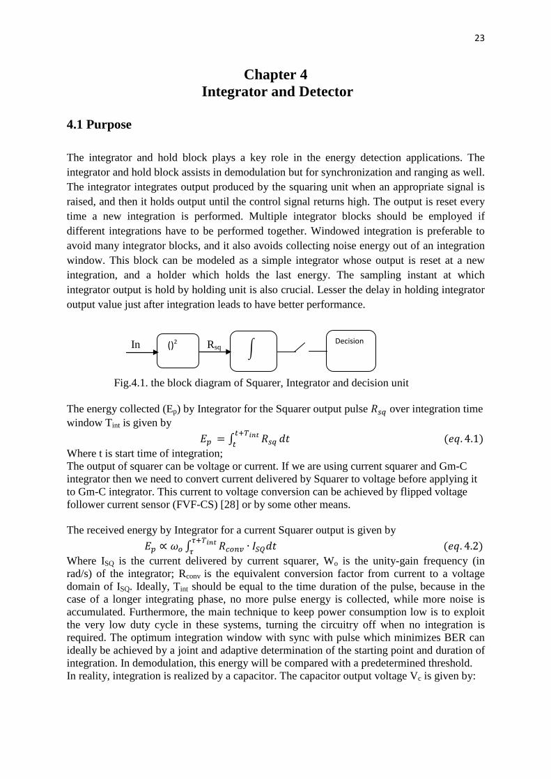
Chapter 4 Integrator and Detector
4.1 Purpose The integrator and hold block plays a key role in the energy detection applications. The integrator and hold block assists in demodulation but for synchronization and ranging as well. The integrator integrates output produced by the squaring unit when an appropriate signal is raised, and then it holds output until the control signal returns high. The output is reset every time a new integration is performed. Multiple integrator blocks should be employed if different integrations have to be performed together. Windowed integration is preferable to avoid many integrator blocks, and it also avoids collecting noise energy out of an integration window. This block can be modeled as a simple integrator whose output is reset at a new integration, and a holder which holds the last energy. The sampling instant at which integrator output is hold by holding unit is also crucial. Lesser the delay in holding integrator output value just after integration leads to have better performance. In Rsq Fig.4.1. the block diagram of Squarer, Integrator and decision unit The energy collected (Ep) by Integrator for the Squarer output pulse 𝑅𝑠𝑞 over integration time window Tint is given by 𝐸𝑝 = ∫ 𝑅𝑠𝑞 𝑑𝑡
𝑡+𝑇𝑖𝑛𝑡𝑡 (𝑒𝑞. 4.1)
Where t is start time of integration; The output of squarer can be voltage or current. If we are using current squarer and Gm-C integrator then we need to convert current delivered by Squarer to voltage before applying it to Gm-C integrator. This current to voltage conversion can be achieved by flipped voltage follower current sensor (FVF-CS) [28] or by some other means. The received energy by Integrator for a current Squarer output is given by
𝐸𝑝 ∝ 𝜔𝑜 ∫ 𝑅𝑐𝑜𝑛𝑣𝜏+𝑇𝑖𝑛𝑡𝜏 ∙ 𝐼𝑆𝑄𝑑𝑡 (𝑒𝑞. 4.2)
Where ISQ is the current delivered by current squarer, Wo is the unity-gain frequency (in rad/s) of the integrator; Rconv is the equivalent conversion factor from current to a voltage domain of ISQ. Ideally, Tint should be equal to the time duration of the pulse, because in the case of a longer integrating phase, no more pulse energy is collected, while more noise is accumulated. Furthermore, the main technique to keep power consumption low is to exploit the very low duty cycle in these systems, turning the circuitry off when no integration is required. The optimum integration window with sync with pulse which minimizes BER can ideally be achieved by a joint and adaptive determination of the starting point and duration of integration. In demodulation, this energy will be compared with a predetermined threshold. In reality, integration is realized by a capacitor. The capacitor output voltage Vc is given by:
()2 Decision

24
𝑉𝐶(𝑡) =1𝐶 𝐼𝑐(𝑡)𝑇
0𝑑𝑡 + 𝑉𝑐(0) (𝑒𝑞. 4.3)
Where, C is the capacitor value, Ic is the capacitor input current, Vc (0) is the capacitor voltage for t = 0. To realize a proper integration function by setting Vc (0) to zero, the capacitor must be discharged after each integration cycle. The output voltage on capacitor is equal to energy collected by integrator. In simple words an integrator is a circuit which has an output voltage that is proportional to the time integral of its input voltage. 4.2. Integrator performance metrics The Integrator performance metrics such as dc gain, unity gain bandwidth, cutoff frequency, slew rate too limits the overall performance of a receiver at a system level. In addition, leakage of integrator also decreases the performance of a receiver. Leakage is reduced by diminish the delay in hold the integrated value. The design of the integrator circuits for high frequency applications become more critical due to inaccuracy in the realization of poles and zeros of integrator filters [29]. The optimum specifications (DC gain, slew rate) finalized from system-level simulations will provide more freedom for circuit designers in the design of integrator filters.In order to find optimal system level parameters for integrator from the system level simulation a detailed study on Integrator was carried out in subsequent sections.
4.2.1 Ideal Integrator vs. Non-Ideal Integrator
Fig.4.2. Magnitude and phase response of integrator [29]
The magnitude and phase responses of an ideal integrator Hid(s) and non-ideal integrator Hni(s) is shown in above Fig.4.2. In reality, the response deviates from the ideal at low frequencies due to finite DC gain and at high frequencies due to parasitic poles and zeros (finite unity bandwidth). 𝑖𝑑𝑒𝑎𝑙 𝑖𝑛𝑡𝑒𝑔𝑟𝑎𝑡𝑜𝑟 𝐻𝑖𝑑(𝑠) =
𝜔0
𝑠 (𝑒𝑞. 4.4)
𝑛𝑜𝑛 𝑖𝑑𝑒𝑎𝑙 𝑖𝑛𝑡𝑒𝑔𝑟𝑎𝑡𝑜𝑟 𝐻𝑛𝑖(𝑠) = 𝐴0(1+𝑠𝑡1)(1+𝑠 𝑡2) (𝑒𝑞. 4.5)
Where 𝜔0 is the unity gain frequency, Ao is DC gain, time constant t1 gives dominant pole p1 and t2 gives parasitic pole p2.

25
For the non-ideal case unity gain frequency approximated by 𝜔0 ≅ 𝐴0/𝑡1 for 1/𝑡1 < 𝜔0 < 1/𝑡2 The quality factor of integrator modeled with transfer function (TF) H(jω)=(R(ω)+jX(ω))-1
is defined as Q(ω)=X(ω)/R(ω). The quality factor indicates the integrator phase deviation from -90. If the integrator is ideal, DC gain and the quality factor would be infinite. 4.3. Integrator Modeling The study is limited to first order integrator filter due to demand of simple and low power consumption circuits by IR-UWB Energy applications. As the order of filter increases the complexity of circuits and power consumption will be increased. In general low-pass filter acts as integrator for the frequencies ten times above its cutoff frequency. Due to this nature, low pass filter used for modeling non ideal integrator. For example, first order LPF with H(s)=wc/(s+wc) acts as integrator for input signal frequencies above ten times filter cutoff frequency (wc) and for a period less than settling period of LPF. The Frequency response and step response of LPF is as shown below. A dc gain Acts as integrator in this frequency range Wc Wu Freq a) Frequency response
A Saturation Integration period Time b) Step response
Fig4.3 LPF as Integrator Where A: Dc gain; Wc: cutoff frequency; Wu: Unity gain band width. Wc=Wu/A 4.3.1 Integrator modeling with Matlab Integrator is modeled with the help of transfer function approach in Matlab from the filter prospective. The filter parameters such as cut-off frequency, DC gain and leakage that affect the integrator performances are further investigated. The known requirement of integrator from previous chapters is its unity gain bandwidth 2GHz.This is due to spread of squarer output is in the band 0 to 2GHz. 4.3.1.1. Ideal Integrator The step response and AC response of Ideal Integrator with finite dc gain represented by H(s)= Adc/s is shown in Fig.4.4 for Adc =1.
Fig.4.4 ideal integrator a) Step response b) Magnitude & phase response

26
4.3.1.2. Non Ideal Integrator The non-ideal integrator with dominant pole at Wo and leakage is given by 𝐻𝑛𝑖(𝑠) = 𝐴𝑑𝑐
𝑠𝜔𝑜
+𝑙𝑒𝑎𝑘𝑎𝑔𝑒 𝑤ℎ𝑒𝑟𝑒 𝑙𝑒𝑎𝑘𝑎𝑔𝑒 ≤ 1 (𝑒𝑞. 4.6)
For example a low pass filter with cutoff frequency 3MHz acts as integrator for the input signal with frequencies greater than 30MHz. To achieve unity gain bandwidth of 2GHz (desired UGBW in our case) for this filter we need to have high dc gain. Unity gain bandwidth =Adc*ωo Adc*ωo=2GHz Adc=2GHz/ωo=2e9/3e6= 666.6666 ≅ 670 = 56.5𝑑𝐵 𝐻𝑛𝑖(𝑠) = 670
𝑠2𝑝𝑖3𝑒6+𝑙𝑒𝑎𝑘𝑎𝑔𝑒
The AC response and DC response of non-ideal integrator with dominant pole at 3MHz and DC gain 56.5dB and different leakage factors 0.01, 0.1 and 1 for step input are shown in below Fig.4.5.
a) Bode plot b) Step response
Fig.4.5. Non ideal integrator From the above plot Fig.4.5 it is observed that as leakage increases then there is a right shift in dominant pole frequency with decrease in dc gain. Slew rate is also affected by leakage which can be seen in step response. As the leakage increase slew starts decreasing. Integrator has to be designed with low leakage and high slew rate. One can also notice from the above graph, for constant unity gain bandwidth, the variation in DC gain shifts dominant pole location. As DC gain decreases from infinity the pole location shifts away from dc. From the above observation, it is concluded that 10 percent decrease in leakage improves dc gain by 20dB and reduces dominant pole frequency by 10percent for constant unity gain bandwidth integrator. By tuning center frequency and keeping the DC gain constant, the unity gain band width will vary as shown below in fig.4.6.

27
(a) (b)
Fig.4.6. Non ideal integrator with constant dc gain a) Bode plot b) Step response For constant dc gain, unity gain bandwidth (GBW) is directly proportional to center frequency (ωo). The blue curve indicates high slew rate, and its pole is near to dc compared to other filter responses. 4.3.1.3. Non Ideal Integrator response for square wave The transient response of integrator 𝐻𝑛𝑖(𝑠) = 670
𝑠2𝑝𝑖3𝑒6+𝑙𝑒𝑎𝑘𝑎𝑔𝑒
for square wave input of
frequency 10MHz and Amplitude 1V is observed with the help of simulink as shown below Fig.4.7.
a) Simulink Implementation of Integrator
b)Square wave of 10MHz input c)Transient response
Fig.4.7. a) Simulink Integrator b) Square wave as input c) Transient response
From this simulation, it is very clear that leakage limits the performance of integrator. Hence leakage should be minimized while designing integrator circuit.
28
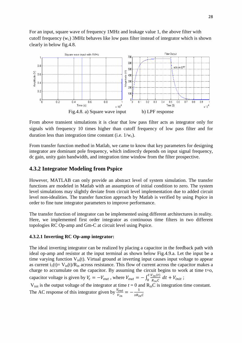
For an input, square wave of frequency 1MHz and leakage value 1, the above filter with cutoff frequency (wc) 3MHz behaves like low pass filter instead of integrator which is shown clearly in below fig.4.8.
Fig.4.8. a) Square wave input b) LPF response
From above transient simulations it is clear that low pass filter acts as integrator only for signals with frequency 10 times higher than cutoff frequency of low pass filter and for duration less than integration time constant (i.e. 1/wc).
From transfer function method in Matlab, we came to know that key parameters for designing integrator are dominant pole frequency, which indirectly depends on input signal frequency, dc gain, unity gain bandwidth, and integration time window from the filter prospective. 4.3.2 Integrator Modeling from Pspice However, MATLAB can only provide an abstract level of system simulation. The transfer functions are modeled in Matlab with an assumption of initial condition to zero. The system level simulations may slightly deviate from circuit level implementation due to added circuit level non-idealities. The transfer function approach by Matlab is verified by using Pspice in order to fine tune integrator parameters to improve performance. The transfer function of integrator can be implemented using different architectures in reality. Here, we implemented first order integrator as continuous time filters in two different topologies RC Op-amp and Gm-C at circuit level using Pspice. 4.3.2.1 Inverting RC Op-amp integrator: The ideal inverting integrator can be realized by placing a capacitor in the feedback path with ideal op-amp and resistor at the input terminal as shown below Fig.4.9.a. Let the input be a time varying function Vin(t). Virtual ground at inverting input causes input voltage to appear as current i1(t)= Vin(t)/Rin across resistance. This flow of current across the capacitor makes a charge to accumulate on the capacitor. By assuming the circuit begins to work at time t=o, capacitor voltage is given by 𝑉𝑐 = −𝑉𝑜𝑢𝑡 , where 𝑉𝑜𝑢𝑡 = −∫ 𝑉𝑖𝑛(𝑡)
𝑅𝑖𝑛𝐶 𝑑𝑡 + 𝑉𝑖𝑛𝑖𝑡
𝑡0 ;
Vinit is the output voltage of the integrator at time t = 0 and RinC is integration time constant. The AC response of this integrator given by 𝑉𝑜𝑢𝑡
𝑉𝑖𝑛= − 1
𝑠𝑅𝑖𝑛𝐶

29
(a)An Active integrator b) AC response
c) Modified RC op-amp integrator
Fig.4.9. Inverting RC op-amp integrator and its ac response At the dc input the op-amp is operating in open loop since capacitor blocks dc. Theoretically, this has to produce infinite output but in practice output of the amplifier saturates at close to power supply of op-amp depending on polarity of input. It’s clear from here that integrator performance will also deviate due to op-amp non linearity like dc offsets, finite bandwidth and op-amp gain. 4.3.2.1.2 Modified/Non-ideal integrator: In order to overcome dc offset of non-ideal op-amp and limited gain at very low frequencies, resistor (Rf) is introduced in parallel to the feedback capacitor as shown in Fig.4.9.c. The feedback resistor provides dc path through which dc current can discharge. The modified integrator transfer function becomes
𝑉𝑜𝑢𝑡𝑉𝑖𝑛
= −
𝑅𝐹𝑅𝑖𝑛
1 + 𝑠𝑅𝐹𝐶
RF should be selected carefully since RF causes the dominant pole frequency of the integrator to move from its ideal location at w=o to one set by 1/RFC and it also limits the dc gain (RF/Rin). Thus selecting RF presents the designer with a trade-off between dc performance and signal performance. A drawback of integrated active-RC circuits is the inaccuracy in the RC time constant, because monolithic resistors and capacitors have a tolerance of more than 20% and do not track each other.

30
1. The Pspice simulation results of inverting RC op-amp integrator: It is modeled as shown in Fig4.10.
Fig.4.10.a) Non ideal Integrator
Fig 4.10.b) Transient simulation Fig.4.10.c)AC Response
Dc gain: -RF/R1=94dB; Integration time constant Ti=RF*CF=0.2us Dominant Pole frequency=1/2*pi* RF*CF =15Hz. In Fig4.10.b transient simulation red curve indicates input square wave of frequency 0.5MHz and green curve indicates the integrator output saturated at -13v equivalent to op-amp supply voltage. Transient simulation shows that Integrator behaves like ideal one until filter gets saturated (due to op-amp saturation). AC response of above integrator filter shows it acts like integrator for input square wave after 100Hz frequency and deviation at low frequencies from ideal integrator response is due to limited dc gain.
31
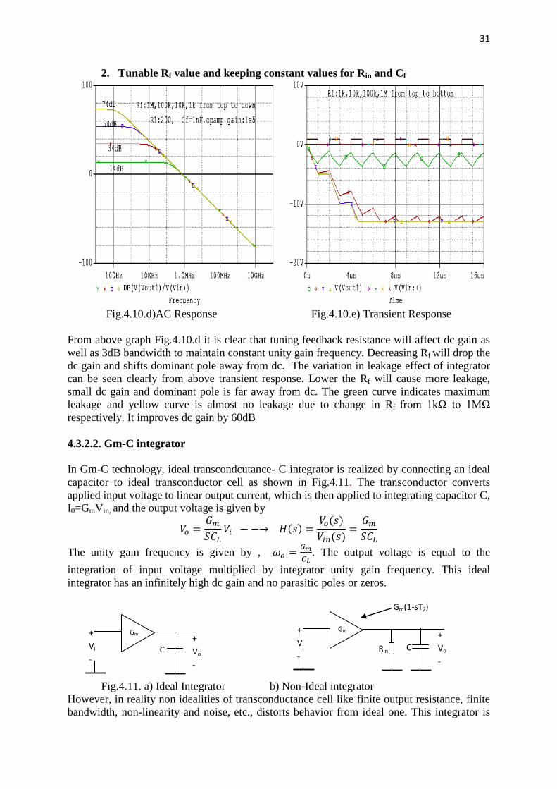
2. Tunable Rf value and keeping constant values for Rin and Cf
Fig.4.10.d)AC Response Fig.4.10.e) Transient Response
From above graph Fig.4.10.d it is clear that tuning feedback resistance will affect dc gain as well as 3dB bandwidth to maintain constant unity gain frequency. Decreasing Rf will drop the dc gain and shifts dominant pole away from dc. The variation in leakage effect of integrator can be seen clearly from above transient response. Lower the Rf will cause more leakage, small dc gain and dominant pole is far away from dc. The green curve indicates maximum leakage and yellow curve is almost no leakage due to change in Rf from 1kΩ to 1MΩ respectively. It improves dc gain by 60dB 4.3.2.2. Gm-C integrator In Gm-C technology, ideal transcondcutance- C integrator is realized by connecting an ideal capacitor to ideal transconductor cell as shown in Fig.4.11. The transconductor converts applied input voltage to linear output current, which is then applied to integrating capacitor C, I0=GmVin, and the output voltage is given by
𝑉𝑜 =𝐺𝑚𝑆𝐶𝐿
𝑉𝑖 −−→ 𝐻(𝑠) =𝑉𝑜(𝑠)𝑉𝑖𝑛(𝑠)
=𝐺𝑚𝑆𝐶𝐿
The unity gain frequency is given by , 𝜔𝑜 = 𝐺𝑚𝐶𝐿
. The output voltage is equal to the integration of input voltage multiplied by integrator unity gain frequency. This ideal integrator has an infinitely high dc gain and no parasitic poles or zeros.
Fig.4.11. a) Ideal Integrator b) Non-Ideal integrator However, in reality non idealities of transconductance cell like finite output resistance, finite bandwidth, non-linearity and noise, etc., distorts behavior from ideal one. This integrator is
Gm + Vi -
+ Vo -
C
Gm + Vi -
+ Vo -
C Rin
Gm(1-sT2)
32
highly sensitive to parasitic capacitors and nonlinear behavior of the transconductor. Hence real Gm-C integrator modeled as first order leaky integrator. 4.3.2.2.1 First order Non-ideal Gm-C integrator Many publications [30] reveal that simple non ideal Gm-C integrator is modeled with transfer function where z1 indicates parasitic zero, Ao is dc gain, and p1 indicates dominant pole
𝐻(𝑠) = 𝐴01 − 𝑠
𝑧11 + 𝑠
𝑝1
In our case simple non ideal integrator realized by placing finite output resistance Rin parallel to integrating capacitor in ideal integrator as shown in fig.4.10 further assuming no parasitic zero. The transfer function changes to
𝐻(𝑠) =𝑉𝑜(𝑠)𝑉𝑖𝑛(𝑠) =
𝐺𝑚𝑅1 + 𝑠𝑅𝐶𝐿
Whereas dc gain given by GmRout and dominant pole shifted from ideal Gm/C to 1/2piRoutC. The fully differential circuits show good noise and distortion properties.
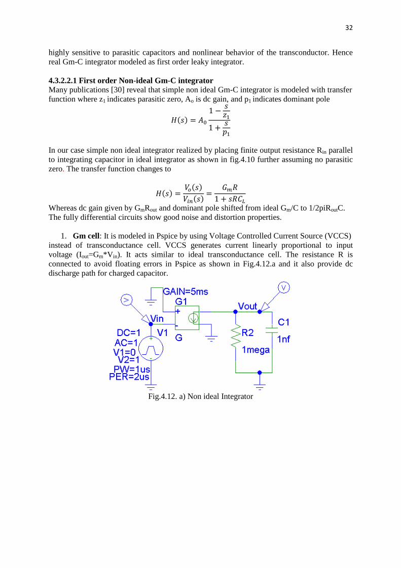
1. Gm cell: It is modeled in Pspice by using Voltage Controlled Current Source (VCCS) instead of transconductance cell. VCCS generates current linearly proportional to input voltage (Iout=Gm*Vin). It acts similar to ideal transconductance cell. The resistance R is connected to avoid floating errors in Pspice as shown in Fig.4.12.a and it also provide dc discharge path for charged capacitor.
Fig.4.12. a) Non ideal Integrator

33
Fig.4.12. b) Transient simulation Fig.4.12. c) AC simulation Dc gain=Gm*R=5k=74dB. Integration time constant Ti=C/Gm=0.2us. Fc=1/2*pi*R*C=160Hz; UGBW=(Gm/C)/(2pi)=0.7MHz. In Fig.4.12.b green curve represents input square wave with 50% duty cycle and red curve represent integrated output wave. Transient simulation shows that above integrator acts like ideal one for input square wave of frequency 0.5MHz. The ac response of integrator shows that it has limited dc gain of 74dB with -20dB/decade slope.
2. Adjustable DC gain
Fig.4.12.e) Transient response Fig.4.12.d) AC response The dc gain is tuned by varying output resistance of Gm-C integrator. From the above transient response Fig.4.12.e it is clear that lower the output resistance will increase the leakage of integrator. The violet curve with Rout: 1k shows more leakage & low slew rate compared to red curve (top one) with Rout: 1M has negligible/no leakage &high slew rate for same square wave input of frequency 0.5MHz. The above graph Fig.4.12.d shows that increasing the output resistance of Gm-C integrator leads to increase in the dc gain. It also causes a shift in dominant pole frequency towards dc and away from unity gain frequency.

34
3. Gm-C with parasitic capacitance The effect of parasitic capacitance on gm-c integrator is studied in this section.
Fig.4.12. f) Gm-C integrator with parasitic capacitance
Fig.4.12.h) transient response Fig.4.12.g) AC Response
Vo=Gm*Vin/(C+Cp)S UGBW=Gm/2*pi*(C+Cp) Parasitic capacitance of transconductance cell at output changes integration time constant, the UGBW and cause linearity problems. From above the transient parametric sweep of parasitic capacitance slew will also change as shown in above Fig.4.12.h. Slew rate decreases as parasitic capacitance increases. The effect of parasitic capacitance on the integration function can be reduced by using miller integrator or by minimizing internal nodes. 4.3.2.3. RC op-amp vs. Gm-C performance comparison The overall performance of integrator is also affected by non-idealities of op-amp or transconductance cell for respective topology of integrator filter along with filter non-idealities as discussed above. The practical op-amp has finite open loop gain and bandwidth limit whereas transconductance cell has no limits on Gm results in large bandwidth. The Gm-C integrator has advantages like… 1. It is based on an open-loop structure. 2. Non dominant pole of Gm-C lies far away from unity gain frequency. 3. Gm-C has no speed limitations compared to op-amp RC. The Gm-C is suitable for high frequency applications in the range several hundred of KHz to more than 100 MHz .Gm-C topology is particularly suitable for energy detection receivers

35
because of linearity and high frequency response, highly tunable and low power dissipation compared to opamp-MOSFET-C and Gm-op-amp-C integrator architectures [31]. The high frequency response is due to absorption of parasitic capacitance [32]. 4.3.3 Integrator Optimization (Matlab to Pspice then to Matlab) The Gm-C integrator response for the squarer output is simulated in this section. The input to integrator is imported from Matlab to Pspice and it is shown in Fig.4.13.b. The frequency of this input signal is 333MHz and duration of pulse is 3ns. The Gm-C filter shown in Fig.4.13 with parameters used in simulation are C: 1pf; Gm: 12.56ms; and variable output resistor(R: 16k, 160k, 1.6M, 16M). The Fig.4.13.b, Fig.4.13.c and Fig.4.13.d shows the input signal, transient response and AC response of filter shown in Fig.4.13.a respectively.
Fig.4.13. a) Gm-C filter
Fig.4.13. b) Input to integrator /Squarer output
Fig.4.13. c) Transient response of Gm-C filter

36
From the transient simulation shown in Fig.4.13.c, lower output resistance will increase the leakage of integrator and decrease slew. Rout increase from bottom to top in the Fig.4.13.c. The green curve indicates lowest Rout and more leakage where as the top blue curve indicates highest Rout, high slew rate and no leakage. As we shift the dominant pole towards dc, and with high dc gain, the leakage will be reduced. It is clear in the Fig.4.13.c, the top black curve indicates large Rout leads to high dc gain, and dominant pole is close to dc compare to others whereas bottom violet curve indicates less dc gain due to low Rout and dominant pole is far away from dc.
Fig.4.13 c) AC response
From the above simulations, a relation between important integrator parameters like cutoff frequency (Fc-int) and frequency (Fsignal) of input signal to be integrated in order to avoid leakage was derived. For the best integrator with no leakage, Fc-int=0.01Fsignal; Adc=UGBW/Fc In other words time constant of integrator must be equal or greater than integration window. In our case best filter parameters for Integrator obtained as Fc-int=0.01Fsignal Fc-int=0.01*333MHZ=3.33MHZ DC gain=2e9/3.33e6=600≅56dB In order to shift the dominant pole towards dc to get ideal integrator response we need to have very high dc gain at the expense of circuit complexity and more power consumption. These are two parameters (dc gain=56dB, UGBW=2GHz) that can be recommended for circuit designer to realize integrator at the circuit level. 4.3.3.1 Pspice to Matlab: The BER evaluation using Matlab and Pspice in the loop is quite complex and takes a lot of time for running simulations. Here Pspice is used for evaluation of Gm-C integrator. Instead of interfacing Pspice to Matlab to export data from Pspice to Matlab for BER evaluation, I have used transfer function approach with dc gain 56dB and Fc: 3.33MHz which gives a similar response as Gm-C filter in Pspice. Then receiver performance in terms of BER is reevaluated using this integrator filter.
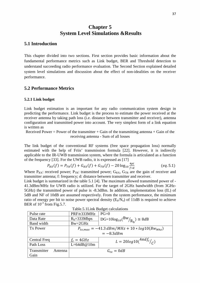
37
Chapter 5 System Level Simulations &Results
5.1 Introduction This chapter divided into two sections. First section provides basic information about the fundamental performance metrics such as Link budget, BER and Threshold detection to understand succeeding radio performance evaluation. The Second Section explained detailed system level simulations and discussion about the effect of non-idealities on the receiver performance. 5.2 Performance Metrics 5.2.1 Link budget Link budget estimation is an important for any radio communication system design in predicting the performance. Link budget is the process to estimate the power received at the receiver antenna by taking path loss (i.e. distance between transmitter and receiver), antenna configuration and transmitted power into account. The very simplest form of a link equation is written as Received Power = Power of the transmitter + Gain of the transmitting antenna + Gain of the
receiving antenna - Sum of all losses The link budget of the conventional RF systems (free space propagation loss) normally estimated with the help of Friis’ transmission formula [22]. However, it is indirectly applicable to the IR-UWB transmission system, where the formula is articulated as a function of the frequency [33]. For the UWB radio, it is expressed as [17] 𝑃𝑅𝑋(𝑓) = 𝑃𝑇𝑅(𝑓) + 𝐺𝑅𝑋(𝑓) + 𝐺𝑇𝑅(𝑓) − 20 log10
4𝑝𝑖𝑓∗𝑑
(𝑒𝑞. 5.1) Where PRX: received power; PTR: transmitted power; GRX, GTR are the gain of receiver and transmitter antenna; f: frequency; d: distance between transmitter and receiver. Link budget is summarized in the table 5.1 [4]. The maximum allowed transmitted power of -41.3dBm/MHz for UWB radio is utilized. For the target of 2GHz bandwidth (from 3GHz-5GHz) the transmitted power of pulse is -8.3dBm. In addition, implementation loss (IL) of 5dB and NF of 10dB are assumed respectively. From the system performance, the minimum ratio of energy per bit to noise power spectral density (Eb/No) of 11dB is required to achieve BER of 10-3 from Fig.5.7.
Table.5.1Link Budget calculations Pulse rate PRF≅333MHz PG=0
DG=10log10(BwRb ) ≅ 8𝑑B Data Rate Rb=333Mbps
Band width Bw=2GHz Tx Power 𝑃𝑡𝑥,𝑚𝑎𝑥 = −41.3𝑑𝐵𝑚 𝑀𝐻𝑧⁄ + 10 ∗ 𝑙𝑜𝑔10(𝐵𝑤𝑀ℎ𝑧)
= −8.3𝑑𝐵𝑚 Central Freq 𝑓𝑐 = 4𝐺𝐻𝑧 𝐿 = 20𝑙𝑜𝑔10(4𝜋𝑑𝑓𝑐
𝐶 ) Path Loss L=64dB@10m Transmitter Antenna Gain
𝐺𝑡𝑥 = 0𝑑𝐵
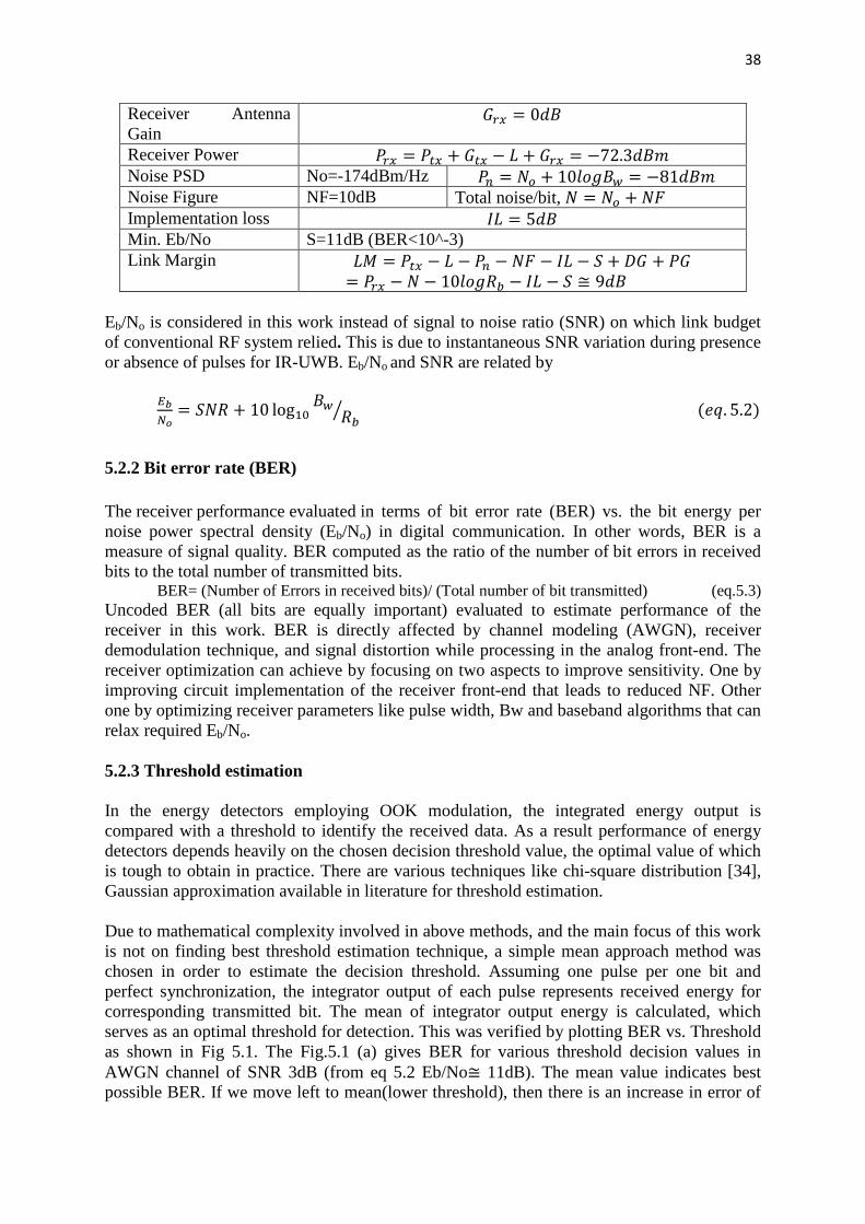
38
Receiver Antenna Gain
𝐺𝑟𝑥 = 0𝑑𝐵
Receiver Power 𝑃𝑟𝑥 = 𝑃𝑡𝑥 + 𝐺𝑡𝑥 − 𝐿 + 𝐺𝑟𝑥 = −72.3𝑑𝐵𝑚 Noise PSD No=-174dBm/Hz 𝑃𝑛 = 𝑁𝑜 + 10𝑙𝑜𝑔𝐵𝑤 = −81𝑑𝐵𝑚 Noise Figure NF=10dB Total noise/bit, 𝑁 = 𝑁𝑜 + 𝑁𝐹 Implementation loss 𝐼𝐿 = 5𝑑𝐵 Min. Eb/No S=11dB (BER<10^-3) Link Margin 𝐿𝑀 = 𝑃𝑡𝑥 − 𝐿 − 𝑃𝑛 − 𝑁𝐹 − 𝐼𝐿 − 𝑆 + 𝐷𝐺 + 𝑃𝐺
= 𝑃𝑟𝑥 − 𝑁 − 10𝑙𝑜𝑔𝑅𝑏 − 𝐼𝐿 − 𝑆 ≅ 9𝑑𝐵 Eb/No is considered in this work instead of signal to noise ratio (SNR) on which link budget of conventional RF system relied. This is due to instantaneous SNR variation during presence or absence of pulses for IR-UWB. Eb/No and SNR are related by 𝐸𝑏
𝑁𝑜= 𝑆𝑁𝑅 + 10 log10
𝐵𝑤𝑅𝑏 (𝑒𝑞. 5.2)
5.2.2 Bit error rate (BER) The receiver performance evaluated in terms of bit error rate (BER) vs. the bit energy per noise power spectral density (Eb/No) in digital communication. In other words, BER is a measure of signal quality. BER computed as the ratio of the number of bit errors in received bits to the total number of transmitted bits.
BER= (Number of Errors in received bits)/ (Total number of bit transmitted) (eq.5.3) Uncoded BER (all bits are equally important) evaluated to estimate performance of the receiver in this work. BER is directly affected by channel modeling (AWGN), receiver demodulation technique, and signal distortion while processing in the analog front-end. The receiver optimization can achieve by focusing on two aspects to improve sensitivity. One by improving circuit implementation of the receiver front-end that leads to reduced NF. Other one by optimizing receiver parameters like pulse width, Bw and baseband algorithms that can relax required Eb/No. 5.2.3 Threshold estimation In the energy detectors employing OOK modulation, the integrated energy output is compared with a threshold to identify the received data. As a result performance of energy detectors depends heavily on the chosen decision threshold value, the optimal value of which is tough to obtain in practice. There are various techniques like chi-square distribution [34], Gaussian approximation available in literature for threshold estimation. Due to mathematical complexity involved in above methods, and the main focus of this work is not on finding best threshold estimation technique, a simple mean approach method was chosen in order to estimate the decision threshold. Assuming one pulse per one bit and perfect synchronization, the integrator output of each pulse represents received energy for corresponding transmitted bit. The mean of integrator output energy is calculated, which serves as an optimal threshold for detection. This was verified by plotting BER vs. Threshold as shown in Fig 5.1. The Fig.5.1 (a) gives BER for various threshold decision values in AWGN channel of SNR 3dB (from eq 5.2 Eb/No≅ 11dB). The mean value indicates best possible BER. If we move left to mean(lower threshold), then there is an increase in error of

39
detecting ‘1’ instead of ‘0’ where as on the right side of mean(higher threshold) there is an increase in error of detecting ‘0’ instead of ‘1’. The Fig.5.1 (b) shows the BER variation with respect to the threshold for different AWGN channel conditions. The increase in the channel SNR or Eb/No causes better BER response. BER is optimum at the optimum threshold. Fig.5.1.b is similar to Fig.5.1(c) except threshold axis is normalized one. Due to the shape of the curve we call this method as bath tub method.
(a) AWGN channel of SNR 3dB (b) Different AWGN channels
(c) Different AWGN channels
Fig.5.1 BER vs. Threshold for selecting Threshold decision value Thresholdoptimal=mean(integrated output energies) Due to continuous fluctuations in the radio channel environment and the signal-to-noise ratio (SNR) it is recommended to use adaptive threshold, which depends on the variation of the signal power and noise power during presence or absence of pulse. From above analysis mean of integrated output energies is chosen as an optimal threshold in further BER evaluation throughout this work. Fig.5.2 shows the importance of threshold decision value for OOK energy detectors. The green line in the middle indicates threshold decision value, and yellow curve indicates the energy collected by Integrator per bit. If bit energy greater than the threshold then received data is binary ‘1’ else binary ‘0’. If the threshold is higher, we may miss detecting bit ‘1’ else if the threshold is lower we may miss detecting bit ‘0’.
Fig.5.2 Visualization of Threshold importance
-1 0 1 2 3 4 5 6
x 10-14
10-3
10-2
10-1
100
Threshold
BE
R
BER vs Threshold @ AWGN channel SNR 3dB
Threshold mean
-1 0 1 2 3 4 5 6 7
x 10-14
10-4
10-3
10-2
10-1
100
ThresholdB
ER
BER vs Threshold for various AWGN channels
SNR: -3dB SNR: -2dBSNR: 1dBSNR: 2dBSNR: 3dB
0 0.2 0.4 0.6 0.8 110
-3
10-2
10-1
100
Normalised Threshold
BE
R
BER vs Threshold for various AWGN channels
SNR:-3dBSNR:-2dBSNR: 1dBSNR: 2dBSNR: 3dB

40
Finally, Comparator or decision circuit decides received data bit ‘di_rx’ by comparing integrated energy ‘Ei’ with a chosen threshold for ith transmitted bit.
𝑑𝑖_𝑟𝑥 = 1 𝑖𝑓 𝐸𝑖 ≥ 0 𝑖𝑓 𝐸𝑖 <
Comparator decides received bit as ‘1’ if the received energy is greater than or equal to threshold otherwise it as bit ‘0’. 5.3 System level implementation Here, simulation results for BER performance of the IR-UWB energy detector receiver under different conditions have been discussed in detail. All the simulations are carried out using MATLAB/Simulink. Performance analysis and comparison of results are discussed in depth after different parametric considerations. The block diagram of Transceiver under simulation is shown in Fig.5.3. The different values for simulation parameters are selected in such a way that whole system meets some standard regulations and have practical applicability. 5.3.1 System level assumptions and system parameters Few assumptions have made during simulation. Some of the basic assumptions listed below: Spreading code is not considered in order to simplify performance evaluation. Only one user uses entire target bandwidth (3GHz-5GHz) of UWB(i.e. one pulse per
bit) The transmitted power is -8.3dBm. Only AWGN channel is considered in this work. Received signals at the receiver have the same power level. Perfect synchronization clock between the transmitter and receiver is assumed.
The various parameters and their values that are used during simulation of results are described in below table.5.2. Parameter Symbol Value Pulse repetition period Tf 3ns Pulse rate PRF 333MHz Transmitted power Ptx -8.3dBm Sampling frequency fs 20GHz Length of transmitted bits N 1e4, 15e4 Modulation OOK Pulse shape 5th order Gaussian Pulse width Tw 3ns Pulse shaping factor Alpha 0.089e-9 Channel model AWGN Tx-RX separation distance D 10m Input amplitude Vpp 0.5mV

41
Fig.5.3 Block diagram of transceiver 5.3.2 Receiver system implementation without RF front-end non idealities The flow chart shown in Fig.5.4, describes the various functional building blocks that have been used for simulations and their sequential flow of the energy detector transceiver under study.
Fig 5.4: flowchart for the simulation of building blocks of energy detector transceiver
Receiver side

42
5.3.2.1 Pulse generation The Matlab program generates pulse waveforms, and transmits the UWB pulse train after OOK modulation of data to be transmitted. The simulation is executed for only one user, and therefore, no spreading code was needed. The process involves pulse generation with the help of Gaussian 5th derivative which can be mathematically expressed as given below [36].
𝑌5(𝑡) = 𝐴 1
𝛼112𝑝𝑖 (−15𝛼4𝑡) + (10𝛼2𝑡3) − 𝑡5𝑒−
𝑡22𝛼2 (𝑒𝑞. 5.4)
Where A: Amplitude, 𝛼: shaping factor(pulse width), t: time. Here variables, A and 𝛼 are chosen to fit with FCC Power spectral density limitation for UWB [35]
(a) Gaussian 5th derivative (c)UWB pulse after BPF
(b) PSD of Gaussian 5th derivative (d) PSD of input pulse after BPF Fig.5.5 UWB pulse and it’s PSD
The Fig.5.5 shows the generated UWB pulse shape and its power spectral density (PSD). As we see PSD of this Gaussian fifth derivative in Fig.5.5 (b) show that power spectrum is not limited to only desire bandwidth from 3GHz to 5GHz. Hence, A band pass filter (BPF) is
0 0.5 1 1.5 2 2.5 3
x 10-9
-5
-4
-3
-2
-1
0
1
2
3
4
5x 10
-4 Input Pulse
Time(ns)
Am
plitu
de(V
)
0 0.5 1 1.5 2 2.5 3
x 10-9
-2.5
-2
-1.5
-1
-0.5
0
0.5
1
1.5
2x 10
-4 Input pulse+bpf
Time(S)
Am
plitu
de
0 1 2 3 4 5 6 7 8 9 10-140
-120
-100
-80
-60
-40
FREQUENCY (GHZ)
psd d
Bm
/Mhz
PSD of Input Pulse
2 2.5 3 3.5 4 4.5 5 5.5 6 6.5 7
-120
-100
-80
-60
-40
Frequency (GHz)
PS
D (
dB
m/M
Hz)
PSD of Transmitted pulse
FCC mask

43
used to limit the pulse power spectrum to the desired frequency band. Fig.5.5(c) and Fig.5.5 (d) it represents time domain and PSD of transmitted pulse, which meets the desired conditions such as low power less than -41.3dBm/MHz, and frequency band of 3GHz-5GHz. 5.3.2.2 Working
IR-UWB non coherent energy detector is better understood in transient simulations. Hence, an ideal OOK non-coherent ED Receiver was simulated in Simulink as shown in Fig5.6(a) and corresponding transient simulations are shown in fig.5.6 (b). The plot in Fig 5.6(b) shows how the OOK modulated signal is demodulated by comparing integrator output energy with a predefined threshold indicated by red line. The transmitted UWB signal with OOK modulation is the top curve followed by AWGN channel response for Eb/No of 11dB, received signal after squarer, Integrator output, and last one indicates reset signal for integrator respectively in Fig 5.6. Where Tp is pulse duration, which is equivalent to 3ns.
Fig.5.6 Energy detection operation with OOK modulation (1 pulse/bit)
out
out
Fig.5.6. (a) ideal OOK-Non-coherent ED Receiver

44
5.3.2.3 Performance evaluation The performance analysis of (BER vs. Eb/No) of the receiver without RF front-end non idealities is shown in Fig 5.7. From this plot Fig 5.7 ideal receiver system shows that AWGN channel of Eb/No with 11dB is needed to achieve BER of 10-3.
Fig:5.7(a) Performance analysis of receiver with out non idealities
5.3.3 Receiver system implementation with RF front-end non idealities The effect of RF front-end non-idealities on receiver performance studied in this section. The flow chart shown in Fig 5.7(b) indicates the procedure followed to map the desired requirements (Sensitivity, link budget) into systems level specifications and to its building blocks throughout this work.
Fig.5.7 (b) Receiver specs flow chart
0 2 4 6 8 10 12 1410
-4
10-3
10-2
10-1
100
Eb/No(dB)
BE
RBER vsEb/No
0.5mv i/p,333Mbps,GLNA:32dB
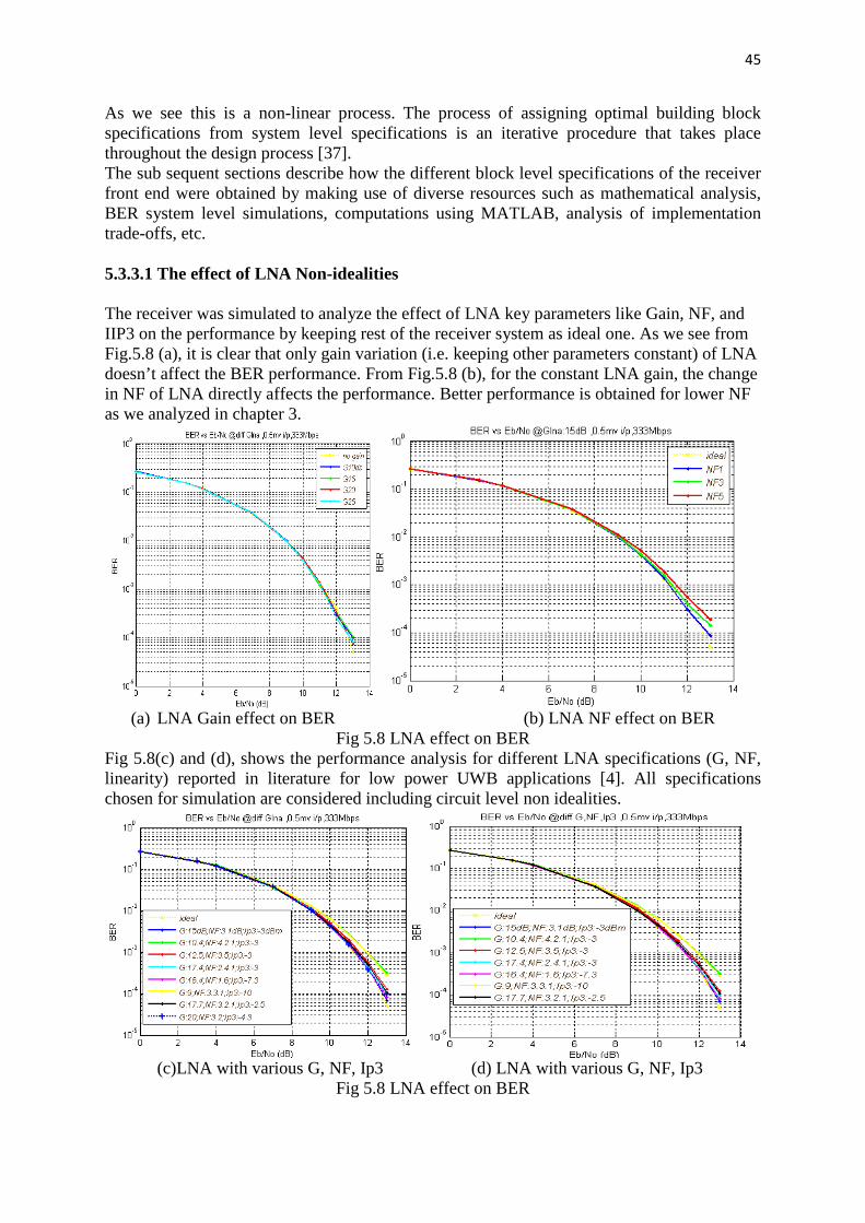
45
As we see this is a non-linear process. The process of assigning optimal building block specifications from system level specifications is an iterative procedure that takes place throughout the design process [37]. The sub sequent sections describe how the different block level specifications of the receiver front end were obtained by making use of diverse resources such as mathematical analysis, BER system level simulations, computations using MATLAB, analysis of implementation trade-offs, etc. 5.3.3.1 The effect of LNA Non-idealities The receiver was simulated to analyze the effect of LNA key parameters like Gain, NF, and IIP3 on the performance by keeping rest of the receiver system as ideal one. As we see from Fig.5.8 (a), it is clear that only gain variation (i.e. keeping other parameters constant) of LNA doesn’t affect the BER performance. From Fig.5.8 (b), for the constant LNA gain, the change in NF of LNA directly affects the performance. Better performance is obtained for lower NF as we analyzed in chapter 3.
(a) LNA Gain effect on BER (b) LNA NF effect on BER
Fig 5.8 LNA effect on BER Fig 5.8(c) and (d), shows the performance analysis for different LNA specifications (G, NF, linearity) reported in literature for low power UWB applications [4]. All specifications chosen for simulation are considered including circuit level non idealities.
(c)LNA with various G, NF, Ip3 (d) LNA with various G, NF, Ip3
Fig 5.8 LNA effect on BER

46
LNA Specifications comparison for low power wideband applications Table 5.3
Gain(dB) NF(dB) IP3(dBm) Ref
15 3.1 -3 [4]
10.4 4.2 -3 [38]
12.5 3.5 -3 [39]
17.4 2.4 -3 [40]
16.4 1.6 -7.3 [4]
9 3.31 -10 [4]
17.7 3.21 -2.5 [4]
From above performance analysis the block level specifications of LNA are chosen as G: 20dB, NF: 3.2dB, IP3=-4.3dBm for the rest of simulations to find out other block level parameters. 5.3.3.2 The effect of Squarer Non-Idealities The following Fig5.9 shows the effect of non-idealities of the square law device (multiplier) on the performance analysis. The receiver was simulated with chosen LNA parameter’s G: 20dB, NF:3.2dB, IP3=-4.3dBm and Variable parameters for squarer and rest of the receiver as ideal one. As we see from the Fig 5.9 (a), it is clear that only gain variation of squarer without considering other squarer parameters doesn’t affect the BER performance, but it improves the output signal amplitude which is required to drive integrator or ADC for analog to digital conversion. From Fig 5.9 (b), for the constant squarer gain, the change in NF of the squarer affects the performance. Lesser the NF better will be the performance. From Fig 5.9 (c) The IIP3 of Squarer affects BER slightly at the higher Eb/No of a channel.
(a)Squarer Gain effect on BER (b) Squarer NF effect on BER (c) Squarer Ip3 effect on BER
Fig.5.9 Squarer Effect on BER

47
(d) Squarer non-idealities effect on BER (e) Squarer non-idealities effect on BER
Fig.5.9 Squarer Effect on BER Fig.5.9 (d) and (e) shows the BER performance variation for different squarer parameters. The squarer specifications chosen for simulation are taken from literature targeting IR-UWB energy detection applications [5][41][42].
Table 5.4 Multiplier Non-idealities from literature Technology BW Gain Vc(dB) NF(dB) IP3(dBm) Ref 0.18um CMOS, 1.8v supply
10 GHz 14 [41]
90nm CMOS 2GHz-4GHz
12.7 @2.4v 14.36 8 [42]
90nm CMOS 5GHz 16 11.05 -1.93 [43] 0.18um CMOS
3-10.6GHz 11 15.7 2 [42]
90nm CMOS 3.1-4.8GHz -14 [5] -10 4 -3 These are
assumed values according to state of art from literature
-14 6 -2 -14 5 2 -16 7 8 -15 6 4
From the above simulation analysis the squarer specifications are chosen as G: 15dB, NF:6; IP3:4dBm. The deviation in performance due to addition of non-idealities of second building block (Squarer) from non-idealities of first building block (LNA) alone is shown in Fig 5.10. The red curve indicates performance analysis due to the non-ideal LNA and blue curve indicate performance analysis due to two non-ideal building blocks (LNA and Squarer). It is clear that non idealities of RF building blocks diminish the overall performance of the receiver. Hence, we have to assign individual block specifications after detail analysis.

48
Fig 5.10 BER vs. Eb/No for ideal and non-ideal LNA &Squarer
5.3.3.3 Integrator Effect on performance The integrator finite bandwidth, dc gain and integration window directly affects overall performance, which is discussed in detail in chapter-4. Fig 5.11 shows the effect of variable DC gain, constant UGBW and fixed integration window of integrator on the BER performance of receiver. As we observe Fig.5.11 (a), higher the DC gain and closer dominant pole to dc of integrator better will be the performance of receiver. The corresponding Integrator filter bode response is as shown in Fig5.11 (b).
(a)Integrator on BER (b) Integrator Bode plot Fig.5.11 The effect of Integrator (variable dc gain, constant UGBW)
5.3.3.3.1 Leakage effect on BER The leakage effect is better understood in time domain simulations.
(a) Squarer unit output b) transient response (c) Leakage effect on BER
Fig.5.12. Integrator Leakage effect on BER
0 2 4 6 8 10 1210
-2
10-1
100
Eb/No (dB)
BER
BER vs Eb/No, 0.5mv i/p,333MbpsLNA: G:32dB, NF:3.2dB,IP3:-4.3dBm
SQ: G:-15dB, NF:6dB,IP3:4dBm
nonideal LNANonideal LNA+SQ
0 2 4 6 8 10 12 1410
-6
10-5
10-4
10-3
10-2
10-1
100
Eb/No (dB)
BE
R
BER vs Eb/No @diff Glna ,0.5mv i/p,333Mbps
36.5db dc56.576.5.96.5
10-3
10-2
10-1
100
101
102
103
0
10
20
30
40
50
60
70
80
90
100
Mag
nitu
de (
dB)
Bode Diagram
Frequency (MHz)
dc gain increases
Fc shifts away from dc
96.5dB
76.5dB
56.5 dB
36.5dB
BER increase by 0.022
No leakage 25% leakage 50% leakage
SNR should be increased by 2.1 dB

49
Fig.5.12 (a) represents the squarer output with its signal content spread in 0-2GHz frequency spectrum. Fig.5.12 (b) shows the transient response of integrator filter 𝐻𝑛𝑖(𝑠) = 670
𝑠2𝑝𝑖3𝑒7+1
for the input in fig5.12 (a). The sampling instant at which integrator output will be on hold decides effective leakage value. This leakage directly affects overall performance, which is shown in Fig.5.13. BER is increased by 0.022 at Eb/No 6dB for delay of 25% of a pulse period in holding integrator output. Similarly, for the delay of 50% of a pulse period in holding integrator output, BER increases by 0.072 at Eb/No 6dB. In other words, for a specific BER of 10-2, the integrator leakage of 25% improves channel Eb/No by 2.1 dB. Lesser the leakage better will be receiver performance. The delay in holding integrator output should be very small as much possible just after the integration time window. From the above analysis, key parameters needed for designing integrator are dominant pole frequency, which indirectly depends on input signal frequency, dc gain, unity gain bandwidth, and integration time window from the filter prospective. Final building-block specifications chosen from above simulations are shown in table 5.5: Gain(dB) NF(dB) IIP3(dBm) LNA+VGA 32 3.2 -4.3 Squarer unit -15 6 4 Integrator 56dB GBW=2GHz

50

51
Chapter 6 Summary and Future work
6.1 Summary: Though an UWB pulse doesn’t have definite shape, Gaussian pulse and its derivative best represents UWB pulses. Gaussian 5th derivative of center frequency 4GHz and pulse period of 3ns which best fit target bandwidth 3GHz to 5GHz was chosen for simulations. The pulse should be modified slightly (by Band pass filter) to fit FCC mask. After brief study of available modulation techniques, OOK modulation was chosen because of less complexity and low power consumption (power required to transmit only for bit ’1’, off for bit ‘0’) needed by target application. In this work, 3GHz - 5GHz non coherent IR-UWB energy detector was implemented at the system level in Matlab. Then non-coherent receiver was simulated with both ideal and non-ideal receiver front end building blocks. There was a decrease in BER performance in non-ideal case compared to ideal receiver front end. Finally, RF front end building block specifications for LNA and Squarer were proposed after BER performance analysis by iterative simulation of the receiver for different block level specifications reported in literature. The integrator leakage effect on BER performance was studied and proposed the relation among key integrator parameters such as dc gain, dominant pole, and frequency of integrator input signal. BER is increased by 0.022 at Eb/No 6dB for integrator leakage of 25%. In other words to achieve a specific BER of 10-2 with the integrator leakage of 25%, channel Eb/No improved by 2.1 dB. Integration window must be less than or equal to the pulse width of signal to be integrated for better performance. If the integration window is larger than pulse width of signal to be integrated, results in more leakage. One of the important finding from integrator analysis is that integrator leakage is unavoidable due to dc discharge path of the capacitor in practice, but it can be minimized by reducing delay in holding integrator output just after integration for detection purpose by threshold comparator. 6.2 Future Work The performance of IR-UWB non-coherent energy detector is not only limited by non-idealities of RF front end blocks and integrator. The receiver performance is also affected by many other parameters few to mention, proper channel estimation, pulse distortion in practice, time synchronization between transmitter and receiver, range, data rate tradeoffs and narrowband interferences (NBI). In order to obtain more practical IR-UWB non-coherent receiver and relax design requirements, this work can be extended further in following research areas. Narrow band interference: Due to large bandwidth occupied by UWB systems, UWB
systems need to coexist with various existing narrowband communication systems. The strong narrow band signals cause interference to UWB systems. Hence this work

52
can be further extended to study the effect of narrow band interferences (NBI) on UWB systems. One way to overcome this NBI on the target UWB systems is to use simple rejection filter. The frequency band of interfere should fall in the stop band of the filter.
Practical conditions: Ideal pulse (Gaussian 5th derivative) transmission was assumed during simulations without considering shape distortion in reality. After proper analysis of channel, transmitter and receiver antennas, more realistic pulse shape can be obtained.
Impact of proper time synchronization and channel estimation: In this work, simulations were done assuming that receiver has perfect knowledge about channel and perfect time synchronization between transmitter and receiver which deviates from reality. Thus, impact of time synchronization and channel estimation on the performance needs further study.
Multi-band UWB Approach: Single band and Multiband are two different approaches exist for UWB wireless communication systems. In single band approach, narrow pulses occupy available bandwidth of 7.5GHz. In the Multi-band approach available bandwidth is divided into smaller sub-bands each with greater than or equal to 500MHz. Single band UWB was considered in this work and it can be extended to multi-band scenario.

53
Bibliography
[1] M.Ghavami, L.ichael, Ryuji kohno, “Ultra Wideband Signals and Systems in Communication,” Wiley; 1st edition 2004.
[2] Intel, “Ultra-wideband (UWB) Technology enabling high-speed wireless personal area networks,” White Paper, 2005. http://www.intel.com/technology/comms/uwb/download/ultra-wideband.pdf
[3] P.Withington II and L.W. Fullerton, "An impulse radio communications system," in Proc. Int. Conf on Ultra- Wide Band, Short-Pulse Electromagnetics, Brooklyn, NY, Oct. 1992, pp. 113- 120.
[4] Z. Zou, David S. M., P. Wang, Q. Zhou, J. Mao, F. Jonsson, H. Tenhunen, L.-R. Zheng, “A Low-Power and Flexible Energy Detection IR-UWB Receiver for RFID and Wireless Sensor Networks,” Circuits and Systems I: Regular Papers, IEEE Transactions on, vol. 58, no. 7, pp. 1470-1482, July 2011.
[5] David Sarmiento M, Zhuo Zou, Qin Zhou, Jia Mao,Peng Wang,Fredrik Jonsson,Li-Rong Zheng “Analog front-end Rx design for UWB Impulse radio in 90nm CMOS” ISCAS:1552-1555.
[6] Ian Oppermann, Matti Hämäläinen, Jari Linatti “UWB Theory and Applications”, jhon wiley and Sons, 2004.
[7] Jorge R.Fernandes, David Wentzloff, “Recent Advances in IR-UWB Transceivers: An Overview” ISCAS’2010.pp.3284-3287 http://www.eecs.umich.edu/wics/publications/Wentzloff_SS_ISCAS2010.pdf
[8] J. H. Reed, “An Introduction to Ultra Wideband Communication Systems”, Prentice Hall, 2005.
[9] S.Rodriguez Duenas, “Design of a DS-UWB Transceiver” (M.Sc Thesis) IMIT/LECS/,2005
[10] D. Cassioli et al., “Performance of low-complexity Rake reception in a realistic UWB channel,” in Proc. IEEE Int. Conf. on Commun., vol.2,pp.763–767,May 2002 http://www.ee.ust.hk/~eezhuxu/UWB/03_Performance%20of%20low%20complexity%20RAKE.pdf
[11] N. He and C. Tepedelenlioglu, “Performance analysis of non-coherent UWB receivers at different synchronization levels,” in Proc. Global Telecommun. Conf., Dallas, TX, Nov.–Dec. 2004, pp. 3517–3521.
[12] L. Yang and G. B. Giannakis, "Analog Space-Time Coding for Multi-Antenna Ultra-Wideband Transmissions,'' IEEE Transactions on Communications, vol. 52, no. 3, pp. 507-517, March 2004 http://www.engr.colostate.edu/~lqyang/publist/tcom04mar.pdf
[13] M.Gufran Khan, “On Coherent and Non-coherent Receiver Structures for Impulse Radio UWB Systems”,M.Sc thesis,2009. http://www.bth.se/fou/forskinfo.nsf/all/d4b47ba7fd9ae895c125756100312a28/$file/mgk_thesis_Final.pdf
[14] H. Zhang and D. Goeckel, “Generalized Transmitted-Reference UWB Systems”, Proceedings of the IEEE Conference on Ultra-Wideband Systems and Technologies (UWBST), November 2003 http://ultra.usc.edu/assets/002/37003.pdf
[15] Vitavasiri, Sinit, "A Non-Coherent Ultra-Wideband Receiver: Algorithms and Digital Implementation," M.Eng. Thesis, Massachusetts Institute of Technology, May 2007.
[16] B. Mihai, “Ultra Wide Band Technologies,” Ad Hoc Mobile Wireless Networks, Research Seminar on Telecommunication Software, autumn 2002.
[17] L. Stoica, "Non-coherent energy detection transceivers for ultra-wideband impulse radio systems," PhD thesis, Faculty of technology of the university of Oulu, Finland, February 2008.

54
[18] H. Nikookar and R. Prasad, Introduction to Ultra Wide Band for Wirless Communications, 2nd ed., Springer, 200
[19] Z.Jinyun, O.Philip, etc., “UWB systems for Wireless sensor networks” TR2009-007,March 2009 http://www.merl.com/reports/docs/TR2009-007.pdf
[20] “First Report and order” Federal communications and commission, 2002 http://hraunfoss.fcc.gov/edocs_public/attachmatch/FCC-02-48A1.pdf.
[21] Zhuo Zou, Jonsson, F., Li-Rong Zheng, Tenhunen, H. , "A digital back-end of energy detection UWB impulse radio receiver," NORCHIP, 2009 , vol., no., pp.1-4, 16-17 Nov. 2009
[22] H. T. Friis, “A Note on a Simple Transmission Formula,” Proc. IRE, Vol.34, no 5, pp. 254-256, May 1946.
[23] “Ultra Wide-Band: State of the Art; Implementation of a Performance- Controllable Low-Noise Amplifier”
[24] Wei Wu; Xiaoya Fan; Tingcun Wei; Charlesy, C.T.; , "A low-voltage low-power self-mixer for 3.1#x2013;5GHz non-coherent UWB receiver," Electron Devices and Solid-State Circuits, 2009. EDSSC 2009. IEEE International Conference of , vol., no., pp.24-27, 25-27 Dec. 2009 http://ieeexplore.ieee.org/stamp/stamp.jsp?tp=&arnumber=5394210&isnumber=5394151
[25] G. Han and E. Sanchez-Sinencio, “CMOS transconductance multipliers: A tutorial,” IEEE Transactions on Circuits and Systems-II: Analog and Digital Signal Processing, vol. 45, no. 12, pp. 1550-1563, December1998.
[26] M.B.Timothy, J.Sungyong, G.Jean, J.Youngjoong, “A CMOS Ultra-wideband differential Low Noise Amplifier”,Proc.of. Asia-Pacific Microwave Conference 2006.
http://ieeexplore.ieee.org/stamp/stamp.jsp?tp=&arnumber=4429452 [27] Tim Merkin, "A CMOS Ultra-Wideband Differential Low Noise Amplifier," M.S.
thesis, The University of Texas at Arlington, December 2005. [28] A.Gerosa, S.Soldà, A.Bevilacqua, D.Vogrig, and A.Neviani, “An energy detector for
non-coherent impulse-radio UWB receivers,” IEEE Trans. Circuits Syst. I: Reg. Papers, vol. 56, no. 5, pp. 1030–1040, 2009.
[29] Heij de, W.J.A. and Seevinck, E. and Hoen. K, “Practical formulation of the relation between filter specifications and the requirements for integrator circuits,” IEEE Transactions on Circuits and Systems, Vol.36. No.8. pp. 1124-1128. August 1989, ISSN 0098-4094.
[30] Vasilevski.M, Aboushady.H, Louerat.M.M, “Automatic Model Refinement of GmC Integrators for High-Level Simulation of Continuous-Time Sigma-Delta Modulators” http://www-soc.lip6.fr/~vasilevs/conf/iscas09.pdf
[31] Mostafa Yargholi and Abdolreza Nabav “CMOS Integrator design for non-coherent UWB receivers,” ICSE 2008 Proc.
[32] W.Ghabrial, L.R. Carley “Transconductance-C filter design for wireless telecommunication receivers” PhD Thesis, Electrical and computer engineering at the Carnegie Mellon University, 2003.
[33] S. Promwon, J.Takada, “Link budget Evaluation Scheme for UWB Transmission systems”, 2005 International Workshop on UWB Technologies, FM4-1, Dec. 2005 (Yokosuka, Japan). http://www.ap.ide.titech.ac.jp/publications/Archive/IWUWBT2005Sathaporn.pdf
[34] M. E. Sahin, I. Guvenc, and H. Arslan, "Joint Parameter Estimation for UWB Energy Detectors Using OOK", in Springer Wireless Personal Commun. Journal, vol. 40, no. 4, pp. 579-591, Mar. 2007.

55
[35] H.Sheng, P.Orlik, A.M.Haimovich, L. J.Cimini, and J.Zhang, “On the spectral and power requirements for ultra-wideband transmission”, IEEE Int. Conf on Communications, Anchorage, AL, USA, vol. 1, pp. 738-742, March 2003
http://ieeexplore.ieee.org/stamp/stamp.jsp?tp=&arnumber=1204271 [36] K. Hyunseok and J. Youngjoong, "Fifth-derivative Gaussian pulse generator for UWB
system," in IEEE Radio Frequency integrated Circuits (RFIC) Symposium, 2005, pp. 671-674 http://ieeexplore.ieee.org/stamp/stamp.jsp?tp=&arnumber=1489903
[37] Alberto Valdes Garcia, “System level design and RF front-end implementation for a 3-10GHz MB-OFDM Ultra wideband receiver and built-in testing techniques for analog and RF integrates circuits,” a Dissertion, Electrical Engineering,Texas A&M University-2006.
[38] A. Bevilacqua and A. M. Niknejad, “An ultra wideband CMOS low noise amplifier for 3.1–10.6-GHz wireless receivers,” IEEE J. Solid State Circuits, vol. 39, no. 12, pp. 2259–2268, Dec. 2004.
[39] J. Hu, Y. Zhu, and H.Wu, “An ultra-wideband resistive-feedback low noise amplifier with noise cancellation in 0.18 m digital CMOS,” in Proc. IEEE Silicon Monolithic Integr. Circuits RF Syst., Jan. 23–25,2008, pp. 218–221.
[40] R. Ramzan, S. Andersson, J. Dabrowski, and C. Svensson, “A 1.4 V 25mW inductor less wideband LNA in 0.13 m CMOS,” in Proc. IEEEInt. Solid-State Circuits Conf., Feb. 11–15, 2007, pp. 424–613
[41] L. Zhou Y. P. Xu, F. Lin, "A gigahertz wideband CMOS multiplier for UWB transceiver," IEEE ISCAS 2005 Dig., vol. 5, pp. 5087-5090, May 2005.
[42] Mincica, M.; Pepe, D.; Zito, D.; , "CMOS UWB Multiplier," Circuits and Systems II: Express Briefs, IEEE Transactions on , vol.58, no.9, pp.570-574, Sept. 2011
[43] R.Apratim, Rashid,A.B.M.H, “Design of a Low Power Compensated 90nm RF Multiplier with Improved Isolation Characteristics for a Transmitted Reference Receiver Front End,” World Academy of Science Engineering and Technology 80 2011

56
Appendix-1 Modeling of nonlinear RF building block using Taylor’s series: According Taylor series, the relationship between input (Vi) and output (Vo) voltages of nonlinear RF building block can be approximated by (1)
Fig:1.Nonlinear RF block Where G:Gain(dB) ; NF=noise figure(dB); IP3= linearity (dBm) are block level specifications of RF building block 𝑉0(𝑉𝑖) = 𝑉𝐷𝐶𝑂 + 𝑎𝑉𝑖 − 𝑏𝑉𝑖2 − 𝑐𝑉𝑖3 − ℎ𝑖𝑔ℎ𝑒𝑟 𝑜𝑟𝑑𝑒𝑟 𝑡𝑒𝑟𝑚𝑠 (1) VDCO is a constant offset voltage and usually not concern because RF circuits usually AC coupled.
Eq (1) is modified as eq (2). 𝑉0(𝑉𝑖) ≅ 𝑎𝑉𝑖 − 𝑏𝑉𝑖2 − 𝑐𝑉𝑖3 − ℎ𝑖𝑔ℎ𝑒𝑟 𝑜𝑟𝑑𝑒𝑟 𝑡𝑒𝑟𝑚𝑠 (2) Here the first order coefficient ‘a’ gives linear gain The other higher order terms distort the output. Second order coefficient ‘b’ is related to second order intercept point Third order coefficient ‘c’ is related to third order intercept point. For differential implementation of RF non-linear block even order terms will be cancelled and leaving only odd order terms. Eq(2) is modified as eq(3) 𝑉0(𝑉𝑖) ≅ 𝑎𝑉𝑖 − 𝑐𝑉𝑖3 − ℎ𝑖𝑔ℎ𝑒𝑟 𝑜𝑟𝑑𝑒𝑟 𝑡𝑒𝑟𝑚𝑠 (3) The first order coefficients ‘a’ and third order coefficient ‘c’ related to block level parameters gain ‘G’ expressed in dB and linearity ‘IP3’ expressed in dBm given by a=sqrt(10^(G/10)
c=4a/3ip3^2 where ip3=10^(IP3/30) Maximum input voltage for clipping= sqrt(a/(3*c));
output voltage at clipping = 2*A/3*Inputmaximum;
RF Non-linear Block
(G, NF, IP3)
Input (Vi) output (Vo)

57
Appendix 2: MATLAB code for receiver system level simulation The main code utilized in simulations given as 7 sub programs
1. Nonideal_LNA_ideal_SQ_integ.m 2. SQ_NF_effect_on_BER.m 3. Integrator_dc_gain_and_leakage_effect_on_BER.m 4. ellip_bpf.m 5. LNA.m 6. Squarer.m 7. psd1.m
1. Nonideal_LNA_ideal_SQ_integ.m %%%%%%%%%%%%%%%%%%%%%%nonideal_lna_ideal_SQ_integ.m%%%%%%%%%%%%%%%%%%%%%%%% %Simulate energy detector with non ideal LNA and ideal Squarer & integrator %LNA NF effet on BER can be observed in the results %%%%%%%%%%%%%%%%%%%%%%%%%%%%%%%%%%%%%%%%%%%%%%%%%%%%%%%%%%%%%%%%%%%%%%%%%%% clear;clc;close all; %%%Transmission parameters Fs=20e9; %Sampling frequency t=-1.5e-9:1/Fs:1.5e-9; %Pulse duration A=0.5e-3; %Amplitude alpha=0.089e-9; %pulse shaping factor num_bits=1e3; %Number of bits to be transmitted %%%System level parameters Eb_over_No_db=[0 2 4 6 8 10 12 14]% AWGN Channel Eb/No values in dB %%%Receiver Block level parameters G,NF in dB, Ip3 in dBm Gain_lna1=32%60%20%[15 10.4 12.5 17 16.4 9 17.7]; NF_lna1=[1 10 20 30]%[3.1 4.2 3.5 2.4 1.6 3.3 3.2]; IP3_lna1=-4.3%[-3 -3 -3 -3 -7.3 10 -2.5] %%%UWB Pulse generation y5=(1/(alpha^11*sqrt(2*pi)))*((-15*alpha^4*t)+(10*alpha^2*t.^3)-(t.^5)).*exp(-t.^2/(2*alpha^2)); y=A*y5/max(y5); t=t+1.5e-9; fb=1/max(t); %data rate %%%Transmit bit sequence d=ones(1,num_bits); for i=1:length(d);% generate alternate '1' & '0's if rem(i,2)==0 d(i)=0; else d(i)=1; end end y_mod=[]; length_singlebit=length(y); %%% OOK Modulation for i=1:length(d); if(d(i)==0) out=0*y; elseif(d(i)==1) out=1*y; end y_mod=[y_mod out];

58
end time_mod=(0:(1/(length(y_mod)-1)):1)*(num_bits*max(t)); %figure(2) %plot(time_mod,y_mod);title('Modulated pulse'); %psd1(y_mod,Fs,time_mod);% title('PSD of pulse train') %%%%energy per bit estimation eb=sum(abs(y_mod(:)).^2)/(length(y_mod(:))*fb)%we find the energy-per-bit, ‘eb’, of our transmitted signal, ‘x’, that %has a bit rate ‘fb’, as: eb = sum(x.^2)/(length(x)*fb) in Matlab. BER_v_th=[]; z=1;BER_var_snr_var_thr=[];v_th_v_snr=[]; mn=1;zz=1 for mk=1:length(NF_lna1);%Gain_squarer);% loop for controlling gain,ip3,NF Gain_lna=Gain_lna1;%(mk); NF_lna=NF_lna1(mk); IP3_lna=IP3_lna1;%(mk); for ebni=Eb_over_No_db; %loop for controlling ebno values errnum=[]; berr=[];errnum_last=[]; EbNo=ebni; ebno=10^(EbNo/10); %to linear value no=eb/ebno; %noise estimation Pn=no*2e9;%Fs/2 %fs/2 noise bw, no is one side noise psd for kkk=1%:15;% more iterations more bits 20e4bits loop for estimating ber values for each ebno value noiseawgn=sqrt(Pn)*randn(1,length(y_mod)); y_awgn=y_mod+noiseawgn; %channel modeling y_filt=ellip_bpf(y_awgn,time_mod); %applying bpf filter at receiver side Y_lna=LNA(Gain_lna,NF_lna,IP3_lna,y_filt); %calling LNA square_out=Y_lna.^2;%ideal Squarer integrator_out=[];integrator_outlast=[];time=[];temp_sq=[]; tx=[];intg_out=[];lm=length_singlebit;intlpf=[]; for n=1:length(d)%for intgration of bit energy temptime=time_mod(1:lm); tempy=square_out(((n-1)*lm+1):lm*n); sqr1=zeros(1,length(y)); sqr1(21:51)=ones(1,31); tempy=tempy.*sqr1; INTOUT1=trapz(temptime, tempy); %for ideal integrator integrator_out=[integrator_out,INTOUT1]; end avg=mean(integrator_out(1:400)); received_data=[];BER_diff_th=[];v_th=[]; for j=1 avg1=avg; received_data1=[]; for i=1:length(integrator_out); if integrator_out(i)>=avg1 received_data1=[received_data1,1]; else received_data1=[received_data1,0]; end end received_data(j,:)=received_data1;

59
BER_diff_th(j,:)=sum(xor(d,received_data(j,:)));%counting num of errors per iteration for sent data end errnum=[errnum BER_diff_th]; % total num of errs BER_diff_th=[]; end berr=sum(errnum)/(kkk*length(d));%BER per specific channel Eb/No %BER_diff_th=berr BER_var_snr_var_thr(z,:)=berr;%[BER_diff_th']; z=z+1; end berout(mn,:)=BER_var_snr_var_thr'; %Each row of berout contains BER values for specific individual block conditions %each row value represents BER for corresponding channel Eb/No values mn=mn+1;z=1; end berout; %Each row of berout contains BER values for specific individual block conditions figure(100) semilogy(Eb_over_No_db,berout(1,:),'b.-',Eb_over_No_db,berout(2,:),'g.-',Eb_over_No_db,berout(3,:),'r.-',Eb_over_No_db,berout(4,:),'c.-') hleg1 = legend('LNA NF: 1dB','Nf: 3dB','NF: 5dB') set(hleg1,'FontAngle','italic','TextColor',[.3,.2,.1]); xlabel('Eb/No (dB)');ylabel('BER');grid on; title('LNA NF effect on BER is observed from BER vs Eb/No for 0.5mv i/p,data rate:333Mbps'); 2. SQ_NF_effect_on_BER.m %%%%%%%%%%%%%%%%%%%%%%SQ_NF_effect_on_BER.m%%%%%%%%%%%%%%%%%%%%%%%%%%%%%%%% %Simulate UWB System for analyzing blck level parameters effect on BER % %For loop mk=1:length(Block(specification)) controlls simulation iterations % %for specific block level specifications % %This program simulates non ideal LNA with "G:32dB, NF:3.2dB,IP3:-4.3dBm", % %non ideal Squarer with "G:-15dB,IP3:4dBm and varaible NF" and % %Ideal integrator and resultant plot gives squarer NF effect on BER % %%%%%%%%%%%%%%%%%%%%%%%%%%%%%%%%%%%%%%%%%%%%%%%%%%%%%%%%%%%%%%%%%%%%%%%%%%% clear;clc;close all; % for clearing all variables %%%Transmission parameters Fs=20e9; %Sampling frequency t=-1.5e-9:1/Fs:1.5e-9; %Pulse duartaion A=0.5e-3; %Amplitude alpha=0.089e-9; %pulse shaping factor num_bits=1e4; %Number of bits to be transmitted %%%System level parameters Eb_over_No_db=[0 3 4 7 9 11 13]; %AWGN Channel Eb/No values in dB %%%Receiver front end block level parameters G,NF in dB, Ip3 in dBm for

60
Gain_lna1=32%[15 10.4 12.5 17 16.4 9 17.7]; %LNA gain in dB NF_lna1=3.2%[3.1 4.2 3.5 2.4 1.6 3.3 3.2]; %LNA NF in dB IP3_lna1=-4.3%[-3 -3 -3 -3 -7.3 10 -2.5] %LNA IP3 in dBm Gain_sq1=-15%[14 12.7 16 11]; %Sqarer Gain in dB IP3_sq1=4%[-2 8 -1.93 2]; %Squarer IP3 in dBm NF_sq1=[4 14.36 11.05 15.07];%6 %Squarer NF in dB %%%UWB Pulse generation y5=(1/(alpha^11*sqrt(2*pi)))*((-15*alpha^4*t)+(10*alpha^2*t.^3)-(t.^5)).*exp(-t.^2/(2*alpha^2)); y=A*y5/max(y5); t=t+1.5e-9;%for shifting pulse to positive time domain Rb=1/max(t); %data rate %%Transmit bit sequence d=ones(1,num_bits); for i=1:length(d);% generate alternate '1' & '0's if rem(i,2)==0 d(i)=0; else d(i)=1; end end y_mod=[]; length_singlebit=length(y); %%% OOK Modulation for i=1:length(d); if(d(i)==0) out=0*y; elseif(d(i)==1) out=1*y; end y_mod=[y_mod out]; end time_mod=(0:(1/(length(y_mod)-1)):1)*(num_bits*max(t)); %%%%energy per bit estimation eb=sum(abs(y_mod(:)).^2)/(length(y_mod(:))*Rb)%we find the energy-per-bit, ‘eb’, of our transmitted signal, ‘x’, that %has a bit rate ‘Rb’, as: eb = sum(x.^2)/(length(x)*Rb) in Matlab. BER_v_th=[]; z=1;BER_var_snr_var_thr=[];v_th_v_snr=[]; mn=1;zz=1 for mk=1:length(NF_sq1);% loop for controlling gain,ip3,NF Gain_lna=Gain_lna1; NF_lna=NF_lna1; IP3_lna=IP3_lna1; Gain_sq=Gain_sq1; NF_sq=NF_sq1(mk); IP3_sq=IP3_sq1; for ebni=Eb_over_No_db; %loop for controlling ebno values errnum=[]; berr=[];errnum_last=[]; EbNo=ebni; ebno=10^(EbNo/10); %converting to linear value no=eb/ebno; %noise estimation Pn=no*2e9; %2e9:noise bw,& no is one side noise psd

61
for kkk=1:20; % for BER estimation for large data (20e4bits); loop for estimating ber values for each ebno value noiseawgn=sqrt(Pn)*randn(1,length(y_mod)); y_awgn=y_mod+noiseawgn; %channel modeling y_filt=ellip_bpf(y_awgn,time_mod); %applying bpf filter at receiver side Y_lna=LNA(Gain_lna,NF_lna,IP3_lna,y_filt); %calling LNA square_out=Squarer(Gain_sq,NF_sq,IP3_sq,Y_lna);%calling Squarer %%% use lpf to filter out of band signal (>2GHz)in Squarer output [na,den]=butter(1,2e9/(0.5*Fs),'low'); y_sing=filter(na, den, square_out); square_out=y_sing; integrator_out=[];time=[];temp_sq=[]; tx=[];intg_out=[];lm=length_singlebit;intlpf=[]; for n=1:length(d)%for intgration of bit energy temptime=time_mod(1:lm); tempy=square_out(((n-1)*lm+1):lm*n); sqr1=zeros(1,length(y)); sqr1(21:51)=ones(1,31); tempy=tempy.*sqr1; %integration window INTOUT1=trapz(temptime, tempy); %for ideal integrator integrator_out=[integrator_out,INTOUT1]; tempy=[]; INTOUT1=[]; end avg=mean(integrator_out(1:400)); received_data=[];BER_diff_th=[];v_th=[]; received_data1=[]; for i=1:length(integrator_out); if integrator_out(i)>=avg received_data1=[received_data1,1]; else received_data1=[received_data1,0]; end end received_data=received_data1; BER_diff_th=sum(xor(d,received_data));%counting num of errors per iteration for sent data errnum=[errnum BER_diff_th]; % total num of errs BER_diff_th=[]; end berr=sum(errnum)/(kkk*length(d));%BER per specific channel Eb/No BER_diff_th=berr BER_var_snr_var_thr(z,:)=[BER_diff_th']; z=z+1; y_awgn=[]; BER_diff_th=[]; end berout(mn,:)=BER_var_snr_var_thr'; %Each row of berout contains BER values for specific individual block conditions %each row value represents BER for corresponding channel Eb/No values mn=mn+1;z=1; end berout; %Each row of berout contains BER values for specific individual block conditions figure(100) semilogy(Eb_over_No_db,berout(1,:),'b.-',Eb_over_No_db,berout(2,:),'g.-',Eb_over_No_db,berout(3,:),'r.-',Eb_over_No_db,berout(4,:),'c.-',Eb_over_No_db,berout(5,:),'m.-','linewidth',2); hleg1 = legend('NF1','NF2','NF3','NF4','NF5');

62
set(hleg1,'FontAngle','italic','TextColor',[.3,.2,.1]); xlabel('Eb/No (dB)');ylabel('BER'); grid on; title('BER vs Eb/No @diff Glna ,0.5mv i/p,333Mbps'); %This plot in figure 100 gives squarer NF effect on BER %Similarly 3. Integrator_dc_gain_and_leakage_effect_on_BER.m %%%%%%%%%%%%%%%%%%%%%%Integrator_dc_gain_and_leakage_effect_on_BER.m%%%%%%% %This program simulates UWB System for analyzing integrator leakage effect on BER %for variable dc gain of integrator with dominant pole at 30MHz %%%%%%%%%%%%%%%%%%%%%%%%%%%%%%%%%%%%%%%%%%%%%%%%%%%%%%%%%%%%%%%%%%%%%%%%%%%%%%% clear;clc;close all; % for clearing all variables %%%Transmission parameters Fs=20e9; %Sampling frequency t=-1.5e-9:1/Fs:1.5e-9; %Pulse duartaion A=0.5e-3; %Amplitude alpha=0.089e-9; %pulse shaping factornn num_bits=1e3; %Number of bits to be transmitted %%%System level parameters Eb_over_No_db=[0 3 4 7 9 11 13]; %AWGN Channel Eb/No values in dB %%%Receiver front end block level parameters G,NF in dB, Ip3 in dBm Gain_lna=32;NF_lna=3.2;IP3_lna=-4.3; %LNA system level specifications Gain_sq=-15;NF_sq=6;IP3_sq=4; %SQuarer specifications dcgain_int1=[10 56]%56.5215; %DC gain of integrator in dB f_dp=3e7; %integrator dominant pole %%%UWB Pulse generation y5=(1/(alpha^11*sqrt(2*pi)))*((-15*alpha^4*t)+(10*alpha^2*t.^3)-(t.^5)).*exp(-t.^2/(2*alpha^2)); y=A*y5/max(y5); t=t+1.5e-9; %for shifting entire pulse into +ve time domain Rb=1/max(t); %gives data rate figure(1) plot(t,y); title('UWB Pulse'); %psd1(y,Fs,t); %Transmit bit sequence d=ones(1,num_bits); for i=1:length(d);% generate alternate '1' & '0's if rem(i,2)==0 d(i)=0; else d(i)=1; end end y_mod=[]; length_singlebit=length(y); %%% OOK Modulation for i=1:length(d); if(d(i)==0) out=0*y; elseif(d(i)==1) out=1*y; end y_mod=[y_mod out];

63
end time_mod=(0:(1/(length(y_mod)-1)):1)*(num_bits*max(t)); %energy per bit estimation eb=sum(abs(y_mod(:)).^2)/(length(y_mod(:))*Rb)%we find the energy-per-bit, ‘eb’, of our transmitted signal, ‘x’, that %has a bit rate ‘Rb’, as: eb = sum(x.^2)/(length(x)*Rb) in Matlab. BER_v_th=[]; z=1;BER_var_snr_var_thr=[];v_th_v_snr=[]; mn=1;zz=1 for mk=1:length(dcgain_int1); %loop for controlling DC gain of integrator dcgain_int=dcgain_int1(mk); for ebni=Eb_over_No_db; %loop for controlling ebno values(i.e different channel conditions) errnum=[]; berr=[];errnum_last=[]; EbNo=ebni; ebno=10^(EbNo/10); %converting to linear value no=eb/ebno; %noise estimation Pn=no*2e9; %2e9:noise bw; no is one side noise psd for kkk=1%:20; %for more iterations gives more bits 20e4 bits and also its loop for estimating ber values for each ebno value noiseawgn=sqrt(Pn)*randn(1,length(y_mod)); y_awgn=y_mod+noiseawgn; %channel modeling y_filt=ellip_bpf(y_awgn,time_mod); %applying bpf filter at receiver side Y_lna=LNA(Gain_lna,NF_lna,IP3_lna,y_filt); %calling LNA square_out=Squarer(Gain_sq,NF_sq,IP3_sq,Y_lna);%calling Squarer %%% use LPF to filter out of band signal (>2GHz)from Squarer output [na,den]=butter(1,2e9/(0.5*Fs),'low'); y_sing=filter(na, den, square_out); %Applying filter square_out=y_sing; %psd1(square_out,Fs,t); integrator_out=[];integrator_outlast=[];time=[];temp_sq=[]; tx=[];intg_out=[];lm=length_singlebit;intlpf=[]; for n=1:length(d)%for intgration of bit energy by seperating single bit information from received signal temptime=time_mod(1:lm); %gives time period of each pulse tempy=square_out(((n-1)*lm+1):lm*n);%gives magnitude of each pulse sqr1=zeros(1,length(y)); % sqr1(21:51)=ones(1,31); tempy=tempy.*sqr1; %Applying integration window %INTOUT2=trapz(temptime, tempy); for ideal integrator dc_linear=10^(dcgain_int/20); h=tf([dc_linear*2*pi*f_dp],[1,(2*pi*f_dp)]); % Integrator with dominant pole at f_dp:30MHz [y_sing tim]=lsim(h,tempy,temptime); %Simulate time response of dynamic system to arbitrary input; similar to filter function %figure(30) %plot(temptime,tempy,temptime,y_sing'); %title('integ input and output'); lpfg=y_sing';

64
INTOUT1=max(lpfg);%For estimating BER without leakage of Integrator INTOUT2=lpfg(length(lpfg));%For estimating BER with leakage of Integrator y_sing=[]; integrator_out=[integrator_out,INTOUT1]; integrator_outlast=[integrator_outlast,INTOUT2]; tempy=[]; INTOUT1=[];INTOUT2=[]; end avg=mean(integrator_out(1:400)); received_data=[];BER_diff_th=[];v_th=[]; received_data_last=[];BER_diff_th_last=[];v_th_last=[]; received_data1=[];received_data_l2=[]; for i=1:length(integrator_out); if integrator_out(i)>=avg received_data1=[received_data1,1]; else received_data1=[received_data1,0]; end if integrator_outlast(i)>=avg received_data_l2=[received_data_l2,1]; else received_data_l2=[received_data_l2,0]; end end received_data=received_data1; received_data_last=received_data_l2; BER_diff_th=sum(xor(d,received_data));%counting num of errors per iteration for sent data BER_diff_th_last=sum(xor(d,received_data_last)); errnum=[errnum BER_diff_th]; % total num of errs errnum_last=[errnum_last BER_diff_th_last]; BER_diff_th=[];BER_diff_th_last=[]; end berr=sum(errnum)/(kkk*length(d));%BER per specific channel Eb/No BER_diff_th=berr berr_last=sum(errnum_last)/(kkk*length(d));%BER per specific channel Eb/No BER_diff_th_last=berr_last; BER_var_snr_var_thr(z,:)=[BER_diff_th']; BER_var_snr_var_thr_last(z,:)=[BER_diff_th_last']; z=z+1; y_awgn=[]; BER_diff_th=[];BER_diff_th_last=[]; end berout(mn,:)=BER_var_snr_var_thr'; %Each row of berout contains BER values for specific individual block conditions %each row value represents BER for corresponding channel Eb/No values klm=mn+1; berout(klm,:)=BER_var_snr_var_thr_last'; mn=klm+1;z=1; end berout; %Each row of berout contains BER values for specific individual block conditions figure(100) semilogy(Eb_over_No_db,berout(1,:),'b.-',Eb_over_No_db,berout(2,:),'g.-',Eb_over_No_db,berout(3,:),'r.-',Eb_over_No_db,berout(4,:),'c.-','linewidth',2);

65
hleg1 = legend('10db dc gain with Noleakage','10db dc gain with leakage','56db dc gain with Noleakage','56db dc gain with leakage'); set(hleg1,'FontAngle','italic','TextColor',[.3,.2,.1]); xlabel('Eb/No (dB)');ylabel('BER'); grid on; title('BER vs Eb/No @diff Glna ,0.5mv i/p,333Mbps; LNA: G:32db,NF:3.2db,IP3_lna:-4.3dbm; SQuarer:G:-15db,NF:6db,IP3:4dbm'); %%In this plot(figure 100) we can observe varaiation in leakage effect due for variable dc gain and integrator efffect on BER 4. ellip_bpf.m %BPF Function: It implements 3GHz-5GHz BPF %Input %input Input Signal sequence %t simulation time sequence %Output %filter_out returns BPF filtered signal %%%%%%%%%%filter%%%%%%%%%%%%%%%%%%%%%%%%%%%%%%%%%%%%%%%%% function filter_out= ellip_bpf(input,t) [N, Wn] = ellipord(1,1.24,1,80,'s'); [B, A] = ellip(N,1,80, Wn, 's'); [num, den] = lp2bp(B, A, 2*pi*3.85e9, 2*pi*2e9); BPF_TF=tf(num, den); %figure(1) % [h,wbp]=freqs(num,den); % plot(wbp*1e-9/2/pi,20*log10(abs(h))); % h=gca; % set(h,'XLim',[0 10],'YLim',[-120 10]); % xlabel('FREQUENCY(GHz)');ylabel('mag (dB)'); % title('BPF Freq response'); filter_out1=lsim(num,den,input,t); filter_out=filter_out1'; %%%%%%%%%%%%%%%%%%%%End of filter%%%%%%%%%%%%%%%%%%%%%%%%%%%%%%%%%%%% 5. LNA.m %LNA Function: It implements LNA behavior. %Inputs %Gain %NF %IP3 LNA non idealities G,NF,IP3 %Yin are Input Signal %Output %out returns modified signal due to LNA. function out=LNA(Gain,NF,IP3,Yin); Rin=50;Rout=50; Gain_linear=10^(Gain/10); a=sqrt(Gain_linear*(Rout/Rin));%first order coefficient IP3_linear=sqrt(2*Rin*10^((IP3-30)/10)); b=(4*a)/(3*IP3_linear^2); %third order coefficient Vin_max=sqrt(a/(3*b)); Vout_max=(2/3)*a*sqrt(a/(3*b)); k=1.38e-23;bw=2e9; noise_variance=bw*4*k*290*Rin*((10^(NF/10))-1); noise=sqrt(noise_variance)*randn(1,length(Yin)); vin=Yin; for i=1:length(vin); if abs(vin(i)) < Vin_max Vout(i)=a*vin(i)-b*vin(i).^3; elseif vin(i) >0

66
Vout(i)=Vout_max; else Vout(i)=-Vout_max; end end out=Vout+noise; end 6. Squarer.m %Squarer Function: It implements Squarer behavior. %Inputs %Gain %NF %IP3 Squarer non idealities G,NF,IP3 %Yin,t are Input Signal and simulation time sequence %Output %out returns modified signal due to Squarer function out=Squarer(Gain,NF,IP3,Yin); Gain_linear=10^(Gain/10); a=sqrt(Gain_linear); Rin=50; IP3_linear=sqrt(2*Rin*10^((IP3-30)/10)); b=(4*a)/(3*IP3_linear^2); %third order coefficient Vin_max=sqrt(a/(3*b)); Vout_max=(2/3)*a*sqrt(a/(3*b)); k=1.38e-23;bw=2e9; noise_variance=bw*4*k*290*Rin*((10^(NF/10))-1); noise=sqrt(noise_variance)*randn(1,length(Yin)); vin=Yin+noise; for i=1:length(vin); if abs(vin(i)) < Vin_max Vout(i)=a*vin(i).^2-b*vin(i).^3; else Vout(i)=Vout_max; end end out=Vout; end 7.psd1.m %PSD Function: It gives power spectral density %Input %y Input Signal sequence %Fs Sampling frequency %t simulation time sequence %Output %gives plot of power spectral density function psd1(y,Fs,t) NFFY=2.^(ceil(log(length(y))/log(2))); NP=NFFY; FFTY=fft(y,NFFY);%pad with zeros NumUniquePts=ceil((NFFY+1)/2); FFTY=FFTY(1:NumUniquePts); MY=abs(FFTY)/length(y); MY=MY.^2; if rem(NP, 2) % MY(2:end)=MY(2:end)*2; else

67
MY(2:end-1)=MY(2:end-1)*2; end f=(0:NumUniquePts-1)*Fs*1e-9/NP; dt=1/Fs; N=length(t); df=1e-6/(N*dt); MY=MY/(df); power=10*log10(MY)+30;%+30 to make it to dbm figure(4) plot(f,power);xlabel('FREQUENCY (GHZ)');ylabel('psd dBm/Mhz'); title('PSD by using FFT')