IMPACT IONIZATION IN SILICON: A REVIEW AND...
14
Solid-State Electronics Vol. 33, No. 6, pp. 705-718, 1990 0038-1101/90 $3.00 + 0.00 Printed in Great Britain. All rights reserved Copyright © 1990 Pergamon Press plc IMPACT IONIZATION IN SILICON: A REVIEW AND UPDATE W. MAES, K. DE MEYER* and R. VAN OVERSTRAETEN IMEC vzw, Kapeldreef 75, 3030 Hevedee, Belgium (Received 4 December 1989; in revised form 23 January 1990) Abstract--After definingthe multiplication factor and the ionization rate together with their interrelation- ship, multiplication and breakdown models for diodes and MOS transistors are discussed. Different ionization models are compared and test structures are discussed for measuring the multiplication factor accurately enough for reliable extraction of the ionization rates. Multiplication measurements at different temperatures are performed on a bipolar NPN transistor, and yield new electron ionization rates at relatively low electrical fields. An explanation for the spread of the experimental values of the existing data on ionization rate is given. A new implementation method for a local avalanche model into a device simulator is presented. The results are less sensitive to the chosen grid size than the ones obtained from the existing method. i. INTRODUCTION Impact ionization is an important charge generation mechanism. It occurs in many semiconductor devices and it either determines the useful characteristic of the device or it causes an unwanted parasitic effect. Let us first consider bipolar devices. The break- down voltage V b of a silicon p-n diode is caused by impact ionization if Vb is larger than about 8 V. The temperature coefficient of Vb is then positive. For breakdown voltages smaller than about 5 V, the breakdown is caused by tunneling. The temperature coefficient of Vb is then negative. In diodes with a breakdown voltage between 5 and 8 V, both mech- anisms contribute to the breakdown and V b is more temperature insensitive, improving the properties of a Zener diode, as a reference voltage. The operation of some devices is based on avalanche generation. This is the case for a thyristor and for an impatt diode. In an avalanche photo- detector, the internal multiplication is used to increase the signal to noise ratio of the total detector system, although avalanche generation produces its own noise due to its statistical behaviour, as explained by McIntyre[1] and Webb[2]. Avalanche generation also plays an increasing role in MOS devices. By scaling down the geometrical dimensions while keeping the supply voltage con- stant, the electrical field increases and therefore impact ionization plays a more important role in device degradation due to hot-carrier effects and bipolar parasitic breakdown. Indeed the hot-carrier degradation phenomena are caused by the electron- hole pairs generated in the high-field drain region of the MOSFET resulting in substrate and in gate *Senior Research Associate of the Belgian National Fund for Scientific Research. currents. Due to hot-electron trapping in the oxide, the threshold voltage V T of the transistor will shift in time and cause reliability problems. Substrate cur- rents can cause bipolar action (latch-up or snap-back) of the MOS transistor. Also breakdown of the drain- substrate junction becomes more important because, due to scaling, the substrate doping must increase in order to avoid punch-through in the device. Many of these problems can be overcome by using LDD- structures, which have a lower electrical field at the drain side, resulting in a lower generation rate. Computer simulation on a specific example shows that a reduction of the peak electrical field by about 40% results in a reduction of the generation rate by a factor of one thousand. In Section 2, the ionization rate and the multipli- cation factor together with their interrelationship are defined. In Section 3, different multiplication and breakdown models are discussed while in Section 4 different ionization models are compared. In Section 5, the parameter extraction procedure for fitting the physical and empirical parameters of the avalanche generation model to the multiplication data on a bipolar transistor at different temperatures is studied. New ionization rate data is given. In Section 6, we discuss the implementation of an avalanche model into a device simulator. A new implementation method, insensitive to the mesh, is introduced. 2. DEFINITION OF THE IONIZATIONRATE AND OF THE MULTIPLICATION FACTOR The ionization rate g is defined as the number of electron-hole pairs generated by a carrier per unit distance travelled. It is different for electrons (~,) and for holes (ap). Impact ionization can only occur when the particle gains at least the threshold energy for ionization E i from the electrical field. From the 705
Transcript of IMPACT IONIZATION IN SILICON: A REVIEW AND...
Solid-State Electronics Vol. 33, No. 6, pp. 705-718, 1990 0038-1101/90 $3.00 + 0.00 Printed in Great Britain. All rights reserved Copyright © 1990 Pergamon Press plc
IMPACT IONIZATION IN SILICON: A REVIEW AND UPDATE
W. MAES, K. DE MEYER* and R. VAN OVERSTRAETEN IMEC vzw, Kapeldreef 75, 3030 Hevedee, Belgium
(Received 4 December 1989; in revised form 23 January 1990)
Abstract--After defining the multiplication factor and the ionization rate together with their interrelation- ship, multiplication and breakdown models for diodes and MOS transistors are discussed. Different ionization models are compared and test structures are discussed for measuring the multiplication factor accurately enough for reliable extraction of the ionization rates. Multiplication measurements at different temperatures are performed on a bipolar NPN transistor, and yield new electron ionization rates at relatively low electrical fields. An explanation for the spread of the experimental values of the existing data on ionization rate is given. A new implementation method for a local avalanche model into a device simulator is presented. The results are less sensitive to the chosen grid size than the ones obtained from the existing method.
i. INTRODUCTION
Impact ionization is an important charge generation mechanism. It occurs in many semiconductor devices and it either determines the useful characteristic of the device or it causes an unwanted parasitic effect. Let us first consider bipolar devices. The break- down voltage V b of a silicon p-n diode is caused by impact ionization if Vb is larger than about 8 V. The temperature coefficient of Vb is then positive. For breakdown voltages smaller than about 5 V, the breakdown is caused by tunneling. The temperature coefficient of Vb is then negative. In diodes with a breakdown voltage between 5 and 8 V, both mech- anisms contribute to the breakdown and V b is more temperature insensitive, improving the properties of a Zener diode, as a reference voltage.
The operation of some devices is based on avalanche generation. This is the case for a thyristor and for an impatt diode. In an avalanche photo- detector, the internal multiplication is used to increase the signal to noise ratio of the total detector system, although avalanche generation produces its own noise due to its statistical behaviour, as explained by McIntyre[1] and Webb[2].
Avalanche generation also plays an increasing role in MOS devices. By scaling down the geometrical dimensions while keeping the supply voltage con- stant, the electrical field increases and therefore impact ionization plays a more important role in device degradation due to hot-carrier effects and bipolar parasitic breakdown. Indeed the hot-carrier degradation phenomena are caused by the electron- hole pairs generated in the high-field drain region of the MOSFET resulting in substrate and in gate
*Senior Research Associate of the Belgian National Fund for Scientific Research.
currents. Due to hot-electron trapping in the oxide, the threshold voltage V T of the transistor will shift in time and cause reliability problems. Substrate cur- rents can cause bipolar action (latch-up or snap-back) of the MOS transistor. Also breakdown of the drain- substrate junction becomes more important because, due to scaling, the substrate doping must increase in order to avoid punch-through in the device. Many of these problems can be overcome by using LDD- structures, which have a lower electrical field at the drain side, resulting in a lower generation rate. Computer simulation on a specific example shows that a reduction of the peak electrical field by about 40% results in a reduction of the generation rate by a factor of one thousand.
In Section 2, the ionization rate and the multipli- cation factor together with their interrelationship are defined. In Section 3, different multiplication and breakdown models are discussed while in Section 4 different ionization models are compared. In Section 5, the parameter extraction procedure for fitting the physical and empirical parameters of the avalanche generation model to the multiplication data on a bipolar transistor at different temperatures is studied. New ionization rate data is given. In Section 6, we discuss the implementation of an avalanche model into a device simulator. A new implementation method, insensitive to the mesh, is introduced.
2. DEFINITION OF THE IONIZATION RATE AND OF THE MULTIPLICATION FACTOR
The ionization rate g is defined as the number of electron-hole pairs generated by a carrier per unit distance travelled. It is different for electrons (~,) and for holes (ap). Impact ionization can only occur when the particle gains at least the threshold energy for ionization E i from the electrical field. From the
705

706 W. MAES et al.
application of the laws of conservation of energy and of momentum at a collision event, it can be derived that a minimum energy of 1.5 E~, with Eg being the bandgap, is needed if the effective masses of both holes and electrons are assumed equal• A large spread of experimental values for E~ exists. In general, the ionization rates (~,.p) depend on the probability for the carriers to reach this threshold energy and this is not only a function of the local electrical field but also of the "history" of the particle; a "non-local" ioniz- ation model thus should be used. As a first approxi- mation a local model is given in which the ionization rate depends only on the local electrical field. The most commonly used local avalanche generation model is the empirical expression of Chynoweth[3], which is similar to the expression for ionization rates in gases:
o~ , , . p= o t ,~ ' pexp ( ~ ) (1)
with ~2p and b,,.p the ionization coefficients and Ej the electrical field component which can be expressed mathematically as:
E.3 E + - I J l " (2)
As can be observed, ~ ~ is the maximum number of carriers that can be generated per unit distance at very high electrical fields. The avalanche generation term is used in the current continuity equations as:
VJ~,p = +q(G~.z, - R..~) (3)
with J.,e the current density for electrons respectively for holes and with G.,p the generation and R.,p the recombination term for electrons and for holes. The plus sign has to be used for holes and the minus sign for electrons. The generation term for avalanche generation can be written as:
G°. _~,,IJ.I ~p14,1 4 (4) q q
It is through these equations that the avalanche generation term is built into a device simulator,
The multiplication factor M is defined as the ratio of the current of one kind (electrons or holes) JovT,~,.p) coming out of a volume to the current of the same kind, J~N.~,.,), flowing into that volume:
M. p - Jouv. t.,p~. (5) • JIN, (n, pt
In one dimension, the relationship between multi- plication and avalanche generation can easily be found by solving the above continuity equation, neglecting the recombination term and knowing that:
"/TOT = J,(x) + Jp(x) (6)
with JTm the total current which must be constant in space. For electrons, as incident carriers[4-6]:
JL _, E(x)
Jout ,n ,.~
J in ,p
0 W
Fig. 1. Simple one-dimensional picture for defining multipli- cation within a certain region W where a high electrical field exists. The sum of hole and electron current must be
constant.
1 M, = w .~ (7)
l-C o -exp (-fo and for holes as incident carriers:
1 M, = w w (8) l-fo % e x p ( - f , . ( , % - ~ . ) d x ' ) d x
where W is the width of the avalanche region as shown in Fig. 1. If a hole and electron current are coming into this region simultaneously, the multi- plication of both current components must be added.
Breakdown is obtained when M ~ w or when:
;7 ( ; ) ~,exp - ( ~ , - % ) d x ' d x = l . (9)
Extracting the ionization coefficients from multipli- cation measurements is not trivial. Indeed, in eqn (7) the integrals cannot be obtained analytically when the electrical field is not constant, which is the case in most devices. The numerical calculation of the inte- gral can be simplified assuming that 7 = (%/~,) is a constant as a function of field, which is valid if the electrical field does not change to much as pointed out by Van Overstraeten and De Man in Refs [7,8]. If the field changes appreciably, the 7 ratio should be taken at the highest field value, because multipli- cation occurs predominantly there. Another difficulty is the fact that the electron and hole ionization coefficients are always appearing together in the equation even when the injected current is of only one type. Parameter extraction therefore is difficult. Yet another source of error is the calculation of the electrical field as a function of distance because the exact doping profile, especially at the junction, must be known. This doping profile can be obtained from C - V measurements as is explained in Refs [4,8,9] or directly out of SRP or SIMS measurements. It should be born in mind, however, that each of these tech- niques suffers from inaccuracies. The determination of the peak electrical field must be very accurate because of the strong dependence of the generation rate on the electrical field.
As pointed out by Beni and Capasso[10] there is also a difference between the increase in current and
Impact ionization in silicon
the increase in the number of generated electron-hole pairs because
Mn p = Jour,(.,p) _ VOUT NOUT (10) ' J IN , (n ,p ) FIN NIN
with VIN(VouT) the carrier velocities and NIN(NouT) the carrier concentrations at the input (output) of the avalanche region. The multiplication factor is due only to pair production (increase in number of carriers), if the carrier velocity is assumed constant over the avalanche region. This is not always true and the difference becomes more pronounced for relatively low electrical fields and for highly doped regions. Only measurements of the multiplication factor on a P - I - N structure would eliminate the influence of the carrier velocity. If multiplication is simulated with a device simulator assuming a constant mobility, the result cannot directly be related to the number of generated electron-hole pairs because the velocity increases linearly with electrical field.
Different approaches to predict the multiplication factor and the breakdown voltage for a given doping profile and structure will be presented in the next section.
3. MULTIPLICATION AND BREAKDOWN MODELS
Instead of using elaborate numerical calculations, it often is useful to have an empirical expression which predicts the multiplication factor of a structure as a function of applied voltage.
3.1. Bipolar diodes
As an example, Miller[5] proposed an empirical formula for the total multiplication factor of a diode as a function of applied voltage:
1 ( ~ ) ~ 1 - ~ = (11)
with Vb the breakdown voltage, n an empirical parameter and M defined as:
Z(V) U = - - 02)
I0
with I 0 the saturation current of the diode[ll] . This relationship holds well for relatively low breakdown voltages, but there is a significant departure for breakdown voltages with an internal field strength below about 350kV/cm. Leguerre[12] used the empirical Miller expression to predict the multipli- cation factor near breakdown by relating the slope factor n to the different materials and substrate dopings.
Fulop[13] proposed the following empirical expres- sion for the ionization rate:
ct = C ( E ) g (13)
with C and g constants which are given for silicon. Using this expression, the breakdown voltage for
707
abrupt and graded junctions can be calculated analytically from the multiplication integral.
Other expressions for the diode breakdown voltage as a function of the doping profile were proposed by several authors[14-17].
Also relations exist to calculate the breakdown voltage of planar junctions with curved edges[18-22] or with field plates[23,24]. The avalanche injection in gate-controlled diodes[25-29] and some transient effects[30] are also studied.
3.2. M O S transistors
Finding the values of the multiplication factor in the drain region of an MOS transistor as a function of gate length and of applied voltage is an important but difficult task. Avalanche multiplication generates the substrate current and part of the gate leakage current. Predicting the multiplication factor analyti- cally is difficult because the electrical field in the drain region has a 2-D character. The validity of a local avalanche generation model as implemented in most device simulators is questionable, since the voltage drop over the avalanche region is rather small com- pared to (Ei /q) , as will be discussed in Section 4 and since the gradient of the electrical field is very high at the drain side. Both these conditions violate the applicability of a local model as is explained more extensively in Section 4. A large number of papers deal with the prediction of MOSFET break- down[31-49].
3.3. Test structures f o r measuring ionization rates
An important topic is the choice of the test struc- ture used to measure the multiplication factor and to extract the ionization rates. The most commonly used structure is a reverse-biased diode in which photons generate the carriers necessary to initiate the ioniza- tion process[8,9,50]. This method is, however, not sensitive enough for measuring very low values of multiplication and thus for determining ionization coefficients at tow electrical fields. For this reason, it is more appropriate to use a test structure which has an internal gain factor for the generated current. Sayle[51] proposed a JFET structure where the initiating current comes from the channel and the generated current is measured in the gate. The problem here is the uncertainty about the electrical field distribution in the avalanche region of the channel. Another interesting device described in Section 5 is the bipolar transistor where the base- collector junction acts as the avalanche region. This structure has two major advantages: the current injected by the emitter can be controlled exactly and second the multiplication can be measured fl times more accurately, fl is the current gain of the transis- tor. This is because the avalanche generated current is superimposed on the base current, which is fl times smaller than the current injected by the emitter and which initiates the generation process. Slotboom[52]
SSE 33/6~H

708 W. MAES et al.
used a bipolar structure for determining the ioniz- ation rate and also a CCD structure with which very small multiplication factors can be detected because the charge packet is multiplied in a serial shift register.
4. T H E D I F F E R E N T A V A L A N C H E I O N I Z A T I O N M O D E L S
In a local model, the ionization rate depends only on the local electrical field and can be written as
ct (xi) = f[E (xi)]. (14)
For a local model to be valid, two conditions must be fulfilled: (i) every individual carrier has to sample a large number of values throughout the whole mo- mentum probability distribution within a distance that is small compared to the mean distance between ionizing encounters and (ii) this distance also has to be small compared to the distance in which the electrical field changes by an appreciable amount. The first condition implies that the total voltage drop over the avalanche region must be several times (El~q). If one of the above conditions is not satisfied, the "history" of the particle should be taken into account for calculating the ionization probability at any location.
The objective of the theory of impact ionization is to derive the probability for an electron to gain from the electrical field an energy at least equal to the threshold energy E~. In the diffusion model of Wolff[53], the electron gains the energy gradually through many collisions. In solving the Boltzmann transport equation, he retains the first two terms in the Legendre polynomial expansion of the energy distribution function, and obtains
ct oc exp (15)
where A is a constant. Shockley[54] argues that the electrons gaining
enough energy from the field are the ones that are lucky enough to avoid collisions. This theory yields:
- E i ~zc exp ( q ~ ) (16)
with l the mean free path. In the theory of Baraff[55,56], higher-order terms
of the Legendre polynomial expansion of the distri- bution function could be retained by using a trunc- ation technique based on the principle of maximum anisotropy. He uses three independent parameters, namely the mean free path, the threshold energy and the energy loss per phonon collision. He also assumes a constant mean free path for both optical phonon and impact ionization scatterings. In the low field region, this theory agrees with Shockley's model and in the high field region with the results of Wolff.
Based on the work of Okuto and Crowell[57] and of Baraff, Thornber[58] derived an expression for the ionization rate valid for all field strengths:
o~ (E) =(qE)~_i exp ( ( E l +--EifffrrE) + E k T ) ( 1 7 )
with E~ the field for which phonon energy is reached in one mean free path, Ekr the field for which the thermal energy kT is reached in one mean free path, and Eif the field for which the threshold energy for ionization is reached in one mean free path. The expression reduces to:
E<EkT ~(E)~(q~ i )
EkT < E < Er ~(E) .~ --~i
(qE) E~<E ~(E)~ ~,
- Ei) exp ~ -
(Thermal) (18)
(Shockley[54]) (19)
(Wolff[53]) (20)
for different electrical field ranges. Thornber used the data published by several
authors to extract parameters for his model. He found a good agreement between the field parameters for the data of Van Overstraeten and De Man[4], Woods[59] and Grant[60] for electrons. For holes, the agreement is not very good. For the effective threshold energy, he found high values (3.6 eV for electrons and 5-6.2eV for holes). This effective threshold energy thus lies well above the nominal one. With respect to the exact values of the parameters, some criticism should be made. Thornber indeed calculated the parameters from ~,.p data, extracted from the multiplication data using the Chynoweth approximation. The correct way would be to use the Thornber expression in the multiplication integral and to fit it to the measured multiplication data.
Recently also the lucky electron model of Shockley has been extended and made suitable for use in a non-local model. Ridley[61-63] differentiated be- tween the rate of momentum and of energy relax- ation, and proposed a lucky drift model which is intermediate between the Shockley and the Wolff model. His results agree well with the ones of Baraff over four orders of magnitude. This model was further improved by Woods[64,65] and Marsland[66] by introducing the concept of "soft threshold en- ergy". Childs[67,68] also includes the effect of field variation over the "dead" space. Chen and Tang[69] use the theory of Keldysh[70], who solved Boltzmann transport equation involving phonon scattering and impact ionization scattering. Chen and Tang derive an explicit expression for the energy mean free path which allows the calculation of Keldysh's energy distribution function. They find a good agreement with the theory of Baraff and of Ridley. They have only one fitting parameter l(EO, characterizing the

Impact ionization in silicon 709
continuous transition from the phonon assisted im- pact ionization to the phononless impact ionization. This mean free path parameter has reasonable values (around 70 A for electrons and 50 A for holes).
To obtain correct simulation results, a non-local generation model should be used in a device simula- tor because the history of the particle has to be taken into account. Attempts are made to use the Monte Carlo technique within a device in the high field region[71]. The recent models discussed above have also tried to account for the "dark space" using the lucky drift theory as a post-processing option. As an example for a non-local model, Childs[68] calculates the probability that an electron acquires the ioniz- ation threshold energy after travelling a distance z~ as:
P(zi)=ff'exp(-~-~) (f"i(zi-z"]dz"] dz (21)
xexp - z \ 2 e ( E ) ] 2 ,] 2
where ;t and 2 E are the mean free paths for momen- tum and energy-relaxing collisions. The ionization rate is therefore characterized by summing the prob- abilities for electrons to drift to the ionization threshold energy as they travel along the channel.
The disadvantage of this method is that it already requires an expression for the electrical field along the channel in order to be able to evaluate the probabil- ities. Other authors[72,73] use other probability func- tions and show simulation results on MOS devices.
Various authors have extracted coefficients for the Chynoweth model from their multiplication measurements, e.g. McKay[74,75], Miller[5], Chyno-
weth[3,76], Lee[77], Moi1178,79], Ogawa[80], Van Overstraeten[8], Grant[60], Dalal[81] and Woods[59]. Their results are summarized in Fig. 2 for electrons and in Fig. 3 for holes (from Ref. [82]). Additionally the results are compared with theoretical calculations of Baraff[55,56] with material constants coming from Sze[83,84]. Also shown are the theoretical limits published by Okuto[57,85] which assume that all the energy the carriers can gain from the field is used to generate other carriers when the threshold energy for ionization is supposed to be 1.6 eV for electrons and 1.8eV for holes as predicted by Hauser[86]. All authors find different parameter couples ( . ,p, b,.p) for the Chynoweth expression to fit their data; as it will be explained in Section 5, this can be caused by a correlation which seems to exist between the parameters ~ and b, for a given data set. The parameter values of Van Overstraeten and De Man are mostly used and seem to give the best simulation results. They extracted their parameters out of a large set of different diodes which automatically optimizes their parameter set for a large number of electrical field profiles as also explained by M~nduteanu[87].
Slotboom[52] extracted avalanche ionization co- efficients for the Chynoweth expression at the surface of an MOS transistor where the generation is smaller due to the roughness of the interface.
Expressions for the temperature dependence of the ionization rate are given by Crowell and Sze[88]. They are in good agreement with the theoretical calculations of Baraff[55]. As the temperature in- creases, the probability for the carriers to reach the threshold energy becomes smaller, and the break- down voltage increases. The temperature dependence
'E o
==
1.0 x 10 s
1.0 X 10⁴
1.0 x 10²
Ogawa (1965) ' . . . .
" ' " . . . . . . . . . . . . . . Van Overstroeten
ond De Mon ( 1 9 7 0 )
~ m x - - - - - - 8 o r o f f - S z e (19621
",13 ~ [] Chynoweth ( 1958 ) %
\ + ~ + L e e - Sze ( 1 9 6 4 )
\ \
1.0 x 10 o I I I I 1.0 x 10 -6 3.0 x 10- 6 5.0 x 10-s 7.0 x 10 .6 9.0 x 10- 6
1 / E ( V / c m )
Fig. 2. Log(or,), given by the Chynoweth model, as a function of electrical field, extracted by various authors.

710 W. M~s et al.
A
~E o v
1 . 0 x 1 0 6
1.0x10⁴
1 . 0 x 1 0 2
" - . . ° ° ° . . . . .
" ' ' ' . . . . . . . . . . . . . . .
\
\ " v
÷\2":,, \\~ \ "~v \+ ",
\ \,, \
O g a w a ( 1 9 6 5 )
~ - - - Van Overstraeten
and De Man ( 1 9 7 0 )
- - - - - - B a r a f f - S z e ( 1 9 6 2 )
. . . . . . . L i m i t . O k u t o ( 1 9 7 2 )
V G r a n t ( 1 9 7 3 )
0 C h y n o w e t h ( 1 9 5 8 )
+ Lee - Sze ( 1964 )
l . O x l O ° I I I I 1.0 x 10 -6 3.Ox 10 -6 5 .0 x 10 - s 7.0 x 10 - 6 9 . 0 x 10 - 6
1/E (V /cm)
Fig. 3. Log(%), given by the Chynoweth model, as a function of electrical field, extracted by various authors.
of the ionization rates is smaller at higher electrical fields. Sutherland[89] found another approximation for the theoretical Baraff curves.
A dependence of ionization rate on crystal orien- tation has not been found[74,77,90].
5. MULTIPLICATION MEASUREMENTS ON A BIPOLAR TRANSISTOR. EXTRACTION PROCEDURE FOR THE
IONIZATION RATE
5. I. General remarks about parameter extraction
From experimental values for the multiplication factor and from an ionization model, it is possible to extract the ionization coefficients from the measured data set. Parameter extraction can be seen as the link between the real physical world (measurements on test structures) and the simulation world (the ioniz- ation model with its parameter values in a device simulator). The task of the extraction program is to find a parameter set for the model which minimizes an error function. This error function is in most cases the root mean square value of the relative differences defined as:
-- ~ ( Si(O)- M'~ 21 (22)
with Mt the measured value of the multiplication factor for the biaspoint i, Si(O) the calculated multi- plication factor for a given parameter vector 0 of the ionization model for bias condition i while N is the number of datapoints. Minimizing this function gives the optimal parameter set for the given data set and given error criterion. It is sometimes preferable to choose a different criterion. If, for example, the measured data set extends over several orders of
magnitude, it is more desirable to take the deviation of the logarithm of the measured quantity. If the obtained coefficient values are implemented in a device simulator, the user must be aware that his simulation results are only valid for the field interval out of which they were extracted.
Good starting values for the fitting process are also important because the residual plane defined by eqn (22) can have more than one minimum, especially if a large number of parameters are fitted simultaneously. Depending on the starting values for the iteration, the fitting algorithm will go to the nearest minimum even if this is a local instead of the global minimum. We used our general purpose parameter extraction pro- gram SIMPAR[91] for the extraction procedure.
Next to finding the optimal parameter values, another important aspect is the calculation of the sensitivity of the different parameters, especially if these values are used for explaining physical phenom- ena. The shape of the residual plane around the minimum tells us how much a parameter may vary in order to increase the residual by a certain amount. It also informs us on how the parameters are correlated to each other. This can be calculated by approxi- mating the residual function by an ellipsoid around the minimum as explained briefly in Appendix A. We will apply this theory to the measurements on our bipolar test structure.
5.2. Experimental results
A special N P N bipolar test structure was developed for the purpose of measuring multiplication factors at relatively low electrical fields. As already described in Section 3, the bipolar transistor is an appropriate structure for measuring low multiplication factors

Impact ionization in silicon 711
1019
A 1018 I
1017
'IA 1016
1015 i , ~ N-
1014 / I I I
f ' - \
I \ / V b c = lOOM 1.0x10 5 [ \ ~ . J
E I \
5.oxio 4 I \ I II \ \ I II \ ~ I I \1 P i i !1 h
0,0 5 10 15 20 Depth (/~m )
Fig. 4. D o p i n g profi le o f the b i p o l a r t r an s i s t o r o b t a i n e d wi th SRP measurement together with the calculated electrical field in the base-collector region for two different values of
because of its internal gain factor. The transistor is processed on an N / N + epi-wafer. The doping profile of the base-collector region, obtained with SRP-measurements, together with the calculated electrical field distribution for two different Vac bias voltages, is shown in Fig. 4. This structure allows the measurement of the multiplication factor at relatively low electrical fields (8.0 x 10⁴-1.5 x 10⁵ V/cm). The N - region has a doping level of about 4.0 x 1014 cm -3 and extends over almost 8 #m. The structure breaks down at the edges for a VBc value of about 100V.
For the measurement, a constant emitter current is injected and the base current is measured for different
I Le = 200boa NPN bipolar transistor
~'~ 5"0 x 10-7 - -0 .0 --
-5.0x10 -7 I I I I I 50 60 70 80 90 100
Vbc ( Volt 1
Fig. 5. Measured base current as a function of Vb¢ for a constant emitter current of 200/~A. AI b is a measure for the
multiplication factor, as given by eqn (23).
Table 1. Extracted ionization parameters for the bipolar transistor measurements at different temperatures
Temp Residual (°c) ~ b, (%)
10 3.010 x 10⁵ 1.135 x 10⁶ 0.5 40 3.318 x 10⁵ 1.174 x 10⁶ 1.5 70 2.990 x l05 1.186 x l06 0.9
100 3.593 x 10⁵ 1.229 x 10⁶ 3.4 130 2.951 x 10⁵ 1.225 x 10⁶ 0.3 160 2.428 x 10⁵ 1.216 × 10⁶ 0.6
Although the fitting residual is very low, no direct relationship between the fitted parameter values as a function of temperature is observed.
Vac values. The value of the current is not critical as long as the mobile carriers do not disturb the elec- trical field in the collector junction. The electrons injected into the collector space-charge region create electron-hole pairs. The holes travel back and the current they generate is superimposed on the base hole current, causing the measured base current to decrease as indicated in Fig. 5. This decrease in base current A/B, is a direct measure of the generated current if the influence of base modulat ion is negli- gible, which is the case for our structure. The decrease AI B can be expressed as:
AIa(VBc ) = IE[M(Fac) - 1] (23)
with I E the injected current in the emitter. These measurements were performed at different tempera- tures between l0 and 160°C, allowing us to investi- gate the temperature dependence of the ionization coefficients.
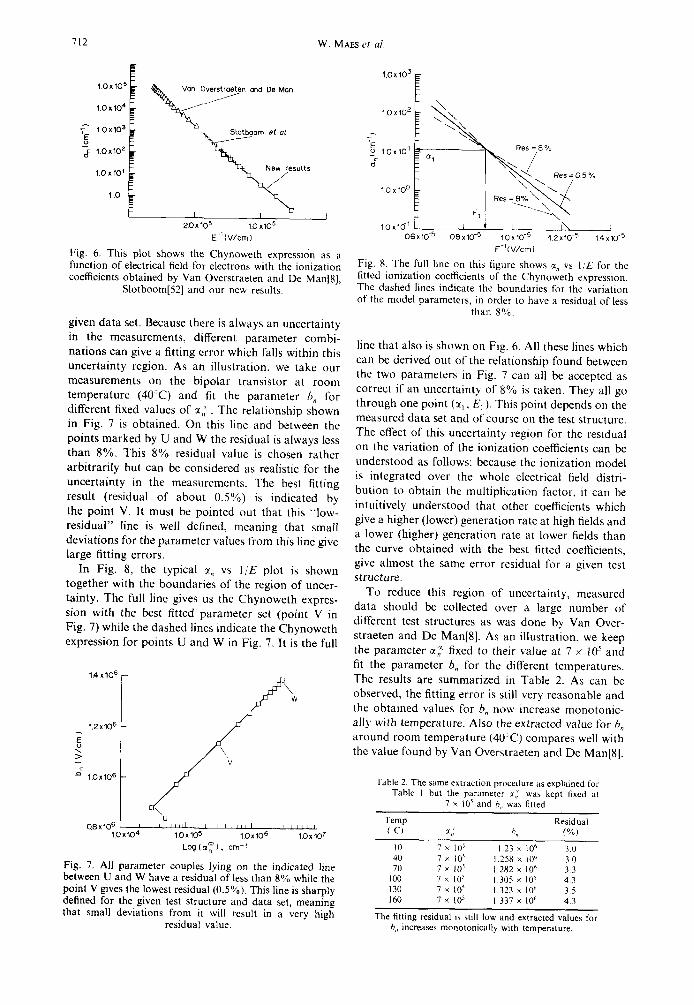
Our parameter extraction program SIMPAR[91] finds a very low sensitivity for the hole ionization coefficients which appear in the multiplication inte- gral. This is normal because the ionization prob- ability for holes is much lower than for electrons, especially for low electrical fields. For this reason, only the ionization rates for electrons are extracted. The extraction results at different temperatures are summarized in Table I. It can be observed that the fitting error is very low. The dependency of the coefficients on temperature will be discussed in the next subsection. Around room temperature (40°C), the results of Van Overstraeten and De Man[8] and the newly obtained ionization coefficients are shown in Fig. 6. The new results extend the older data to lower electrical fields. The agreement with the extrapolated Van Overstraeten and De Man data is excellent. Also the recent data of Slotboom et al. in the intermediate electrical field range are shown. They used also a bipolar transistor to deter- mine the low multiplication values and their data are also in agreement with our data.
5.3. Discussion o f the obtained extraction results
As shown in Figs 2 and 3, different authors find strongly different ionization coefficients as optimal parameter values for their measurements. A possible explanation for this discrepancy can be the inter- action between the two coefficients ~t ~ and b for a
712 W. MAES et al.
1.0x10⁵ ~ Von O ~ e n ond De Mon
1.0 x 10⁴
~" 1.0x10 s m" = i,~ Slotboom et at
1.0 x l O 2 mr E ] ~
t.O x 101 ~ e s u tts
1.0
I I I 2.0 x 10⁵ 1.0 x 10⁵
E -~ (V/cm)
Fig. 6. This plot shows the Chynoweth expression as a function of electrical field for electrons with the ionization coefficients obtained by Van Overstraeten and De Man[8],
Slotboom[52] and our new results.
given data set. Because there is always an uncertainty in the measurements, different parameter combi- nations can give a fitting error which falls within this uncertainty region. As an illustration, we take our measurements on the bipolar transistor at room temperature (4ffC) and fit the parameter b, for different fixed values of ~ , ' . The relationship shown in Fig. 7 is obtained. On this line and between the points marked by U and W the residual is always less than 8%. This 8% residual value is chosen rather arbitrarily but can be considered as realistic for the uncertainty in the measurements. The best fitting result (residual of about 0.5%) is indicated by the point V. It must be pointed out that this "low- residual" line is well defined, meaning that small deviations for the parameter values from this line give large fitting errors.
In Fig. 8, the typical % vs I/'E plot is shown together with the boundaries of the region of uncer- tainty. The full line gives us the Chynoweth expres- sion with the best fitted parameter set (point V in Fig. 7) while the dashed lines indicate the Chynoweth expression for points U and W in Fig. 7. It is the full
1~ xlO 6 \
w
1.2x10⁶
,..;, - \ .~ 1.0x10 6
u Q 8 x 1 0 6 I t I I I l l l l l [ I I I l i l l l I I I ~ l [ l l ]
I O x l O 4 1,0X10⁵ 1.0X10⁶ I O x l O z
Log (an~), crn-'~
Fig. 7. All parameter couples lying on the indicated line between U and W have a residual of less than 8% while the point V gives the lowest residual (0.5%). This line is sharply defined for the given test structure and data set, meaning that small deviations from it will result in a very high
residual value.
1.0x 10³
1.0 x 102 " " ~ ,
~ " ~ Res = 8 %
~ x ~ , Res = °5 °/°
IOxi0 -I ~ t I I"% t Q6xlO -5 Q8xlO -5 1.0x10 -5 1.2x10 -5 14x10 -5
E-l(V'/cmj
Fig. 8. The full line on this figure shows ~, vs I /E for the fitted ionization coefficients of the Chynoweth expression. The dashed lines indicate the boundaries for the variation of the model parameters, in order to have a residual of less
than 8%.
line that also is shown on Fig. 6. All these lines which can be derived out o f the relationship found between the two parameters in Fig. 7 can all be accepted as correct if an uncertainty of 8% is taken. They all go through one point (~1, E~ ). This point depends on the measured data set and of course on the test structure. The effect of this uncertainty region for the residual on the variation of the ionization coefficients can be understood as follows: because the ionization model is integrated over the whole electrical field distri- bution to obtain the multiplication factor, it can be intuitively understood that other coefficients which give a higher (lower) generation rate at high fields and a lower (higher) generation rate at lower fields than the curve obtained with the best fitted coefficients, give almost the same error residual for a given test s t ruc ture .
To reduce this region of uncertainty, measured data should be collected over a large number of different test structures as was done by Van Over- straeten and De Man[8]. As an illustration, we keep the parameter ~,~'- fixed to their value at 7 × 10⁵ and fit the parameter b, for the different temperatures. The results are summarized in Table 2. As can be observed, the fitting error is still very reasonable and the obtained values for b,, now increase monotonic- ally with temperature. Also the extracted value for b,, around room temperature (40°C) compares well with the value found by Van Overstraeten and De Man[8].
Table 2. The same extraction procedure as explained for Table 1 but the parameter %; was kept fixed at
7 × 10⁵ and b~ was fitted
Temp Residual ( C ) :~/ ho (%)
10 7 x 10⁵ 1.23 × 10⁶ 3.0 40 7 x l0 s 1.258 x 10⁶ 3.0 70 7 x 10⁵ 1.282 x 10⁶ 3,3
I00 7 x 10⁵ 1.305 x 10⁶ 4.3 130 7 x 10⁵ 1.323 x 10⁴ 3.5 160 7 x | 0 s 1337 x 10 ~ 4.3
The fitting residual is still low and extracted values for b. increases monotonical ly with temperature.
Impact ionization in silicon 713
To see whether the relationship between ¢t ~ and b also holds for another test structure and for higher electrical fields, a diode profile is simulated and the multiplication data are generated with the coefficients given in Ref. [8]. We find an uncertainty relation between ~t and I/E totally similar to the one given in Fig. 8, proving that our considerations about the relationship between ~t ~ and b are general. This explains the rather large discrepancy between the experimental ct vs I /E results of several authors, as shown in Figs 2 and 3. In contrast with Van Over- straeten and De Man, most authors measured their ionization rates on a very limited number of diodes and using one device structure. Within a reasonable uncertainty of the measurements, the ~t vs E relation can be rotated around a certain point (~tj,E~) as shown in Fig. 8. Taking this consideration into account, most experimental results can be made to agree rather well.
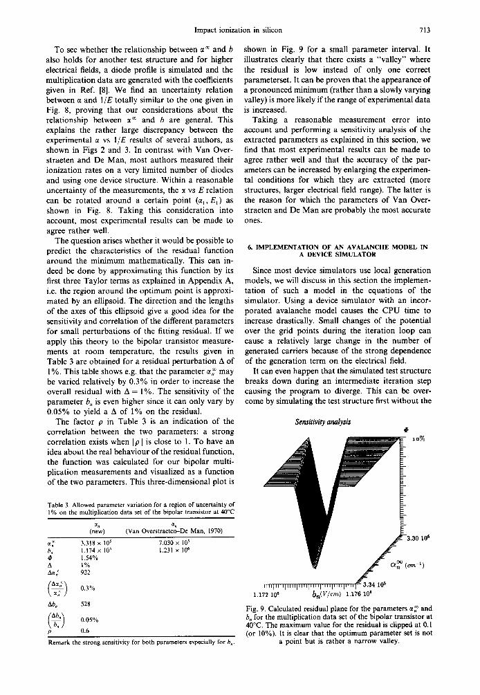
The question arises whether it would be possible to predict the characteristics of the residual function around the minimum mathematically. This can in- deed be done by approximating this function by its first three Taylor terms as explained in Appendix A, i.e. the region around the opt imum point is approxi- mated by an ellipsoid. The direction and the lengths of the axes of this ellipsoid give a good idea for the sensitivity and correlation of the different parameters for small perturbations of the fitting residual. If we apply this theory to the bipolar transistor measure- ments at room temperature, the results given in Table 3 are obtained for a residual perturbation A of 1%. This table shows e.g. that the parameter ct, ~ may be varied relatively by 0.3% in order to increase the overall residual with A = 1%. The sensitivity of the parameter b, is even higher since it can only vary by 0.05% to yield a A of 1% on the residual.
The factor p in Table 3 is an indication of the correlation between the two parameters; a strong correlation exists when I P [ is close to 1. To have an idea about the real behaviour of the residual function, the function was calculated for our bipolar multi- plication measurements and visualized as a function of the two parameters. This three-dimensional plot is
shown in Fig. 9 for a small parameter interval. It illustrates clearly that there exists a "val ley" where the residual is low instead of only one correct parameterset. It can be proven that the appearance of a pronounced minimum (rather than a slowly varying valley) is more likely if the range of experimental data is increased.
Taking a reasonable measurement error into account and performing a sensitivity analysis of the extracted parameters as explained in this section, we find that most experimental results can be made to agree rather well and that the accuracy of the par- ameters can be increased by enlarging the experimen- tal conditions for which they are extracted (more structures, larger electrical field range). The latter is the reason for which the parameters of Van Over- straeten and De Man are probably the most accurate ones.
6. IMPLEMENTATION OF AN AVALANCHE MODEL IN A DEVICE SIMULATOR
Since most device simulators use local generation models, we will discuss in this section the implemen- tation of such a model in the equations of the simulator. Using a device simulator with an incor- porated avalanche model causes the C P U time to increase drastically. Small changes of the potential over the grid points during the iteration loop can cause a relatively large change in the number of generated carriers because of the strong dependence of the generation term on the electrical field.
It can even happen that the simulated test structure breaks down during an intermediate iteration step causing the program to diverge. This can be over- come by simulating the test structure first without the
Sensitivity analysis @
,%
Table 3. Allowed parameter variation for a region of uncertainty of 1% on the multiplication data set of the bipolar transistor at 40°C
~n ~n (new) (Van Overstraeten-De Man, 1970)
~t~ 3.318 x 10 ~ b, 1.174 × ] 0 6
1.54% A I% A~t~ 922
Ab, 528
p 0.6
7.030 x l05 1.231 x l06
Remark the strong sensitivity for both parameters especially for b,.
lO s
')
~,q,,~,l~,,q~.~l,,~l,~,~l,,~q,,,,~3.34 10 s 1.172 106 bn(Y/cm) 1.176 106
Fig. 9. Calculated residual plane for the parameters ~ and b, for the multiplication data set of the bipolar transistor at 40°C. The maximum value for the residual is clipped at 0. l (or 10%). It is clear that the optimum parameter set is not
a point but is rather a narrow valley.

714 W. MAES et al.
Ve ~ N~ Pdln =N" i i i . I Depletion
V b ~ p ~ =~Regi°n (W
Vc
Jout
Fig. 10. Definition of the simulated bipolar structure with our 2-D device simulator PRISM. The collector base junc- tion consists of a lowly doped region where the electrical field is constant over W = 1 pm width. The hole and elec- tron currents can be calculated at different values of VBv.
The recombination term is taken as zero.
ava lanche term. Then these in termedia te results can be used as a s tar t ing point for the s imulat ion with the ava lanche generat ion term included.
Ano the r source of error is the discret izat ion of the structure. If the discret izat ion mesh is coarse, the results can be e r roneous even when the p rogram converges. This is clearly i l lustrated with the s imulat ion of a simple N P N bipolar t rans is tor as shown in Fig. 10. The problem is essentially one-d imens ional so the compute r s imulat ion can easily be compared with exact analytical calculations. The l # m wide collector region conta ins a lightly- doped N region where the electrical field is constant . For the s imulat ion, the recombina t ion term is ex- cluded, al lowing us to calculate exactly bo th the current injected by the emit ter and the base hole current as a funct ion of applied base-col lec tor voltage. The s imulated results and the analytical calculat ions are compared in Fig. 1 I. When the high-field collector region is divided into ten mesh points in the direct ion of the current , the s imulated current vs base--collector voltage agrees very well
8 o
• -~ 60 One mesh-p
~ 40
2O
Cotcutotecl 0 I t I I
329000 331000 333000 335000 337000 E ( V/cm )
Fig. 11. The simulated multiplication factors on the struc- ture defined in Fig. 10 as a function of electrical field over the base-collector junction by discretizing this region re- spectively with one meshpoint and with ten meshpoints in the direction of the current. The computed results are
compared with analytically calculated values.
E
E
Fig. 12. A piece of a finite difference mesh around the node i. A cell which contains all near neighbour points can be constructed around the node. For each sub-triangle of the cell, a different current and electrical field can be deter-
mined.
with the analytically calculated values. If this same collector region is discretized with only one mesh- point , the mult ipl icat ion deviates f rom the analytical solution and the devia t ion becomes larger as the electrical field increases. The conclusion is tha t even when there is a region with a very low doping level where the voltage drop is linear, a fine grid is required to correctly simulate the current increase due to ava lanche generat ion.
A practical app roach is to derive a me thod to implement a local generat ion model in a way which is a lmost grid independent . To illustrate the problem, the way the generat ion term is used in most device s imulators is studied. The current cont inui ty eqn (3) can be discretized using the divergence theorem, and referring to the 2-D finite e lement mesh of Fig. 12, in the following way for node i:
2 J , , , p 4 , = Z a""~ "J~ i neighb .... "" p T (24)
with A~.~. k the area and G the generat ion rate over the whole mesh triangle. The sum must be taken over all ne ighbour n o d e s j of node i. The currents are defined on the lines between the nodes with d,, / the length of the bisectors of the different node lines. A r o u n d each node, a cell is created which conta ins all points nearest to tha t node. Tha t is the reason why only one third of the area of all ne ighbour ing mesh-tr iangles must be taken into account in the generat ion term of the per t inent node. The left side of this equat ion is solved s imultaneously with all o ther equat ions in an internal coupled loop of the device simulator. The r igh t -hand side (generat ion term) must be re- calculated between every iteration. It is this calcu- lation which int roduces the sensitivity to the chosen mesh. This term is implemented in most 2-D device s imulators by
~,,p(Ej)lJo, pl G,,.p ~ (25)
q
The advantage of this formula is its simplicity, but the d rawback is tha t the result is only correct for very small-sized triangles. This difficulty can be overcome by taking the direct ion of the current J and the shape
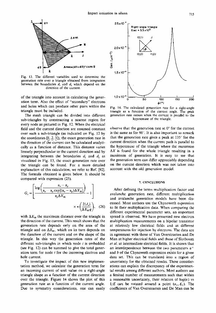
Impact ionization in silicon 715
*Axrn/2
Fig. 13. The different variables used to determine the generation rate over a triangle obtained from integration between the boundaries d~ and d 2 which depend on the
direction of the current.
of the triangle into account in calculating the gener- ation term. Also the effect of "secondary" electrons and holes which can produce other pairs within the triangle must be included.
The mesh triangle can be divided into different sub-triangles by constructing a nearest region for every node as pictured in Fig. 12. When the electrical field and the current direction are assumed constant over such a sub-triangle (as indicated on Fig. 12 by the coordinates [1, 2, 3]), the exact generation rate in the direction of the current can be calculated analyti- cally as a function of distance. This distance varies linearly perpendicular to the current direction and by integrating between the boundaries dl and dE as visualized in Fig. 13, the exact generation rate over the triangle can be found. For a more detailed explanation of this calculation, we refer to Ref. [92]. The formula obtained is given below. It should be compared with expression (25).
G. = log e . _ ~ p e x p [ ( e . - ep)AXM]] 1
<xpAXM
x . ( 2lJ . I "~ (26) \ AXMq J'
with AXM the maximum distance over the triangle in the direction of the current. This result shows that the generation rate depends only on the area of the triangle and on AXM, which on its turn depends on the direction of the current and on the shape of the triangle. In this way the generation rates of the different sub-triangles in which node i is embedded (see Fig. 12) can be summed to give the total gener- ation term for node i for the incoming electron and hole current.
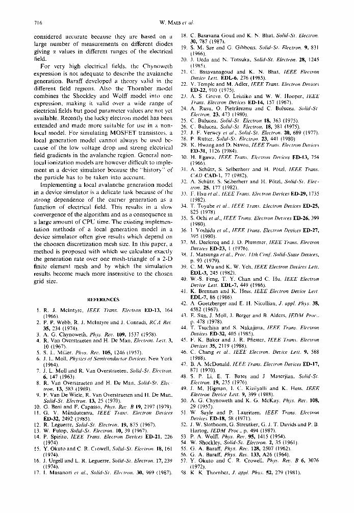
To investigate the impact of this new implemen- tation method, we calculate the generation term for an incoming current of unit value on a right-angle triangle shape as a function of the current direction over the triangle. Figure 14 shows the plot of this generation rate as a function of the current angle. Due to symmetry considerations, one can easily
2.5 x 10⁻⁴ r Right-angLe trion0to L Elec - 3.3 x10 5
1.5 x 10 . 4
1.0 x 10 ~ I I 0 50 100 150 200
~ ( ° )
Fig. 14. The calculated generation rate for a right-angle triangle as a function of the current angle. The peak generation rate occurs when the current is parallel to the
hypotenuse of the triangle.
observe that the generation rate at 0 ° for the current is the same as for 90 ° . It is also important to remark that the generation rate gives a peak at 135 ° for the current direction when the current path is parallel to the hypotenuse of the triangle where the maximum AX is found for the whole triangle resulting in a maximum of generation. It is easy to see that the generation term can differ appreciably depending on the current direction which was not taken into account with the old generation model.
7. CONCLUSIONS
After defining the terms multiplication factor and avalanche generation rate, different multiplication and avalanche generation models have been dis- cussed. Most authors use the Chynoweth expression to fit their multiplication data. When comparing the different experimental parameter sets, an important spread is observed. We have presented new electron multiplication measurements on a bipolar transistor at relatively low electrical fields and at different temperatures for injection by electrons. The data are in agreement with those of Van Overstraeten and De Man at higher electrical fields and those of Slotboom et aL at intermediate electrical fields. It is shown that an interdependence between the two parameters ~t ~ and b of the Chynoweth expression exists for a given data set. This can be translated into a region of uncertainty for the obtained results. These consider- ations can explain the discrepancy of the experimen- tal results among different authors. Most authors use a limited number of measurements such that within a reasonable uncertainty, their relation of log(~t) vs 1/E can be rotated around a point (cq,E~). The coefficients of Van Overstraeten and De Man can be
716 W. MAES et al.
considered accurate because they are based on a large n u m b e r of measurements on different diodes giving ~ values in different ranges of the electrical field.
For very high electrical fields, the Chynoweth expression is not adequate to describe the ava lanche generat ion. Baraff developed a theory valid in the different field regions. Also the T h o r n b e r model combines the Shockley and Wolff model into one expression, making it valid over a wide range of electrical fields but good pa ramete r values are not yet available. Recently the lucky electron model has been extended and made more suitable for use in a non- local model. For s imulat ing M O S F E T transistors, a local generat ion model canno t always be used be- cause of the low voltage drop and s t rong electrical field gradients in the ava lanche region. Genera l non- local ionizat ion models are however difficult to imple- ment in a device s imula tor because the "h i s to ry" of the particle has to be taken into account.
Implement ing a local ava lanche generat ion model in a device s imula tor is a delicate task because of the s t rong dependence of the carr ier generat ion as a funct ion of electrical field. This results in a slow convergence of the a lgor i thm and as a consequence in a large a m o u n t of C P U time. The existing implemen- ta t ion me thods of a local generat ion model in a device s imula tor often give results which depend on the choosen discret izat ion mesh size. In this paper, a me thod is proposed with which we calculate exactly the generat ion rate over one mesh-tr iangle of a 2-D finite element mesh and by which the s imulat ion results become much more insensitive to the chosen grid size.
REFERENCES
1. R. J. Mclntyre, 1EEE Trans. Electron ED-13, 164 (1966).
2. P. P. Webb, R. J. Mclntyre and J. Conradi, RCA Rev. 35, 234 (1974).
3. A. G. Chynoweth, Phys. Rev. 109, 1537 (1958). 4. R. Van Overstraeten and H. De Man, Electron. Lett. 3,
10 (1967). 5. S. L. Miller, Phys. Rev. 105, 1246 (1957). 6. J. L. Moll, Physics of Serniconductor Devices. New York
(1964). 7. J. L. Moll and R. Van Overstraeten, Solid-St. Electron.
6, 147 (1963). 8. R. Van Overstraeten and H. De Man. Solid-St. Elec-
tron. 13, 583 (1969). 9. F. Van De Wiele, R. Van Overstraeten and H. De Man,
Solid-St. Electron. 13, 25 (1970). 10. G. Beni and F. Capasso, Phys. Rev. B 19, 2197 (1979). 11. G. V. M~nduteanu, IEEE Trans. Electron Devices
ED-32, 2492 (1985). 12. R. Leguerre, Solid-St. Electron. 19, 875 (1967). 13. W. Fulop, Solid-St. Electron. 10, 39 (1967). 14. P. Spirito, IEEE Trans. Electron Devices ED-21, 226
(1974). 15. Y. Okuto and C. R. Crowell, Solid-St. Electron. 18, 161
(1974). 16. J. Urgell and L. R. Leguerre, Solid-St. Electron. 17, 239
(1974). 17. I. Masanori et al., Solid-St. Electron. 30, 969 (1987).
18. C. Basavana Goud and K. N. Bhat, Solid-St. Electron. 30, 787 (1987).
I9. S. M. Sze and G. Gibbons, Solid-St. Electron. 9, 831 (1966).
20. J. Ueda and N. Totsuka, Solid-St. Electron. 28, 1245 ( 1985).
21. C. Basavanagoud and K. N. Bhat, IEEE Electron Device Lett. EDL-6, 276 (1985).
22. V. Temple and M. Adler, IEEE Trans. Electron Devices ED-22, 910 (1975).
23. A. S. Grove~ O. Leistiko and W. W. Hooper, IEEE Trans. Electron Devices ED-14, 157 (1967).
24. A. Rusu, O. Pietrfireanu and C. Bulucea, Solid-St. Electron. 23, 473 (1980).
25. C. Bulucea, Solid-St. Electron 18, 363 (1975). 26. C. Bulucea, Solid-St. Electron. 18, 381 (1975). 27. J. F. Verwey et al., Solid-St. Electron. 20, 689 (1977). 28. P. Rutter, Solid-St. Electron. 23, 441 (1980). 29. K. Hwang and D. Navon, IEEE Trans. Electron Devices
ED-31, 1126 (1984). 30. H. Egawa, IEEE Trans. Electron Devices ED-13, 754
(1966). 31. A. Schfitz, S. Selberherr and H. P61zl, IEEE Trans.
CAD CAD-l, 77 (1982). 32. A. Schfitz, S. Selberherr and H. P6tzl, Solid-St. Elec-
tron. 25, 177 (1982). 33. F. Hsu et al., IEEE Trans. Electron Devices ED-29, 1735
(1982). 34. T. Toyabe et al., IEEE Trans. Electron Devices ED-25,
825 (1978). 35. S. Ochi et al., 1EEE Trans. Electron Devices ED-26, 399
(1980). 36. 1. Yoshida et al., IEEE Trans. Electron Devices ED-27,
395 (1980). 37. M. Declercq and J. D. Plummer, IEEE Trans. Electron
Devices ED-23, 1 (1976). 38. J. Matsunga et al., Proc. l lth Con[~ Solid-State Devices,
p. 93 (1979). 39. C. M. Wu and K. W. Yeh, IEEE Electron Devices Lett.
EDL-3, 245 (1982). 40. W.-S, Feng, T. Y. Chan and C. Hu, IEEE Electron
Device Lett. EDL-7, 449 (1986). 41. K. Brennan and K. Hess, IEEE Electron Device Lett.
EDL-7, 86 (1986). 42. A. Goetzberger and E. H. Nicollian, J. appl. Phys. 38,
4582 (1967). 43. E. Sun, J. Moll, J. Berger and B. Alders, IEDM Proc.,
p. 478 (1978). 44. T. Tsuchiya and S. Nakajima, 1EEE Trans. Electron
Devices ED-32, 405 (1985). 45. F. K. Baker and J. R. Pfiester, IEEE Trans. Electron
Devices 35, 2119 (1988). 46. C. Chang et al., 1EEE Electron. Device Lett. 9, 588
(1988). 47. B. A. McDonald, IEEE Trans. Electron Devices ED-17,
871 (1970). 48. S. P. Li, E. T. Bates and J. Maserjian, Solid-St.
Electron. 19, 235 (1976). 49. J. M. Higman, I. C. Kizilyalli and K. Hess, IEEE
Electron Device Lett. 9, 399 (1988). 50. A. G. Chynoweth and K. G. McKay, Phys. Rev. 108,
29 (1957). 51. W. Sayle and P. Lauritzen, IEEE Trans. Electron
Devices ED-18, 58 (1971). 52. J. W. Slotboom, G. Streutker, G. J. T. Davids and P. B.
Hartog, 1EDM Proc., p. 494 (1987). 53. P. A. Wolff, Phys. Rev. 95, 1415 (1954). 54. W. Shockley, Solid-St. Electron. 2, 35 (1961). 55. G. A. Baraff, Phys. Rev. 128, 2507 (1962). 56. G. A. Baraff, Phys. Rev. 133, A26 (1964). 57. Y. Okuto and C. R. Crowell, Phys. Rev. B 6, 3076
(1972). 58. K. K. Thornber, J. appl. Phys. 52, 279 (1981).

Impact ionization in silicon 717
59. M. H. Woods, W. C. Johnson and M. A. Lampert, Solid-St. Electron. 16, 381 (1973).
60. W. N. Grant, Solid-St. Electron. 16, 1189 (1973). 61. B. K. Ridley, J. Phys. C: Solid-State Phys. 16, 3378
(1983). 62. B. K. Ridley, J. Phys. C: Solid-State Phys. 16, 4733
(1983). 63. B. K. Ridley, Semicond. Sci. Technol. 2, 116 (1987). 64. R. C. Woods, IEEE Trans. Electron Devices ED-34,
1116 (1987). 65. R. C. Woods, Appl. Phys. Lett. 52, 65 (1988). 66. J. S. Marsland, Solid-St. Electron. 30, 125 (1987). 67. P. A. Childs, J. Phys. C: Solid-State Phys. 20, L243
(1987). 68. P. A. Childs, NASCODE V--Proc. fifth Int. Conf.
Numerical Analysis of Semiconductor Devices and Integrated Circuits, pp. 17-19, Dublin (1987).
69. Y. Z. Chen and T. W. Tang, J. appl. Phys. 65, (1989). 70. L. V. Keldysh, Soy. Phys. JETP 21, 1135 (1965). 71. S. Bandyopadhyay, M. Klausmeier-Brown, C. Maziar,
S. Datta and M. Lundstrom, IEEE Trans. Electron Devices ED-34, 392 (1987).
72. T. Thurgate and N. Chan, IEEE Trans. Electron Devices ED-32, 400 (1985).
73. R. Kuhnert, C. Werner and A. Schfitz, IEEE Trans. Electron Devices ED-32, 1057 (1985).
74. K. G. McKay and K. B. McAfee, Phys. Rev. 91, 1079 (1953).
75. K. G. McKay, Phys. Rev. 94, 877 (1954). 76. A. G. Chynoweth, J. appl. Phys. 31, (1964). 77. C. A. Lee et al., Phys. Rev. 134, A761 (1964). 78. J. J. Moll and N. I. Meyer, Solid-St. Electron. 3, 155
(1961). 79. J. J. Moll and N. I. Meyer, Solid-St. Electron. 6 (1963). 80. T. Ogawa, Jap. J. appl. Phys. 6, 473 (1963). 81. V. L. Dalai, Appl. Phys. Lett. 15 (1969). 82. S. Selberherr, S. Sch/itz and H. P6tzl, Two Dimensional
MOS Transistor Modeling, Summer Course on VLSI Process and Device Modeling, Katholieke Universiteit Leuven, Belgium (1983).
83. S. M. Sze and G. Gibbons, Appl. Phys. Lett. 5 (1966). 84. S. M. Sze, Physics of Semiconductor Devices. Wiley,
New York (1981). 85. Y. Okuto and C. R. Crowell, Phys. Rev. B 10 (1974). 86. J. R. Hauser, J. appl. Phys. 37, 507 (1966). 87. G. V. MSnduteanu, Int. J. Electron. 56, 555 (1984). 88. C. R. Crowell and S. M. Sze, Appl. Phys. Lett. 9, 242
(1966). 89. A. D. Sutherland, IEEE Trans. Electron Devices ED-27,
1299 (1980). 90. V. M. Robbins et al., J. appl. Phys. 58, 4614 (1984). 91. W. Maes, K. De Meyer and L. Dupas, IEEE Trans.
CAD CAD-5, 320 (1986). 92. Esprit Report: Esprit 962E-17, Progress in Work
package 1: Physical models and Validation (1989). 93. Y. Bard, Non-linear Parameter Estimation. Academic
Press, New York (1974).
A P P E N D I X
Sensitivity Calculation on Extracted Parameter Values
In general, data fitting and parameter extraction are carried out mathematically by minimizing a specified objective function 4" (0). For any proposed analytical multi- plication model, the objective function can be specified as follows,
4" = ~. (Si(O) - M , y l (27) ,=,\ ~ ] N
with Mi the measured multiplication factor, N the number of data points and Sj(O) the calculated multiplication factor for a given model parameter vector 0. The extraction
omin ~_ . . . . I
I I
+ Popt Pi
Fig. A1. This simple picture illustrates the shape of the residual plane around the optimal parameter value together
with a region of uncertainty A.
oo O~ n
Region of uncertainty
/ ~min+A
~min
bn Fig. A2. Visualization of the contour plots showing the region of uncertainty for the two parameters ~ ~ and b,. This region is assumed to be an ellipsoid which has the dimension
of the number of parameters.
program calculates a best fit parameter vector O* but due to the experimental uncertainties, there is no reason to prefer O* above any other value of 0 for which
14"(0) - 4 ' ( 0 " ) 1 ~ E (28)
where ~ is an allowed fitting error caused by experimental uncertainties. These uncertainties can have different origins. A first error source can come from noise on the measure- ments. It can also arise from the fact that the model itself is not perfect in describing the given physical phenomena or that the test structure is not correctly characterized. All these error sources create an uncertainty interval for the different parameters.
One way of calculating this region of uncertainty is by approximating the E indifference region by an ellipsoid. Therefore, the problem of parameter uncertainty is now converted into the problem of the determination of the length and orientation of the ellipsoidal axes. The residual function is expanded in a Taylor series keeping only the first three terms:
4" (0) = 4" (0") + J ' r 60 + ½60XH*60, (29)
with 0 the parameterset, 60 = ( 0 - 0") while J* and H* are the Jacobian (first derivatives with respect to the par- ameters) and the Hessian matrix (second derivatives with respect to the parameters) evaluated in the minimum 0 ' . This is clearly illustrated in Fig. A1 which shows the error function for one parameter and in Fig. A2 showing the contour plots for two parameters. Because the Taylor expansion is evaluated in the minimum of the residual plane, the Jacobian matrix will be zero. The Hessian matrix is defined as
=F 024" 1 H,,j Loo,oo? j. ( 3 0 )
718 W. MAES et al.
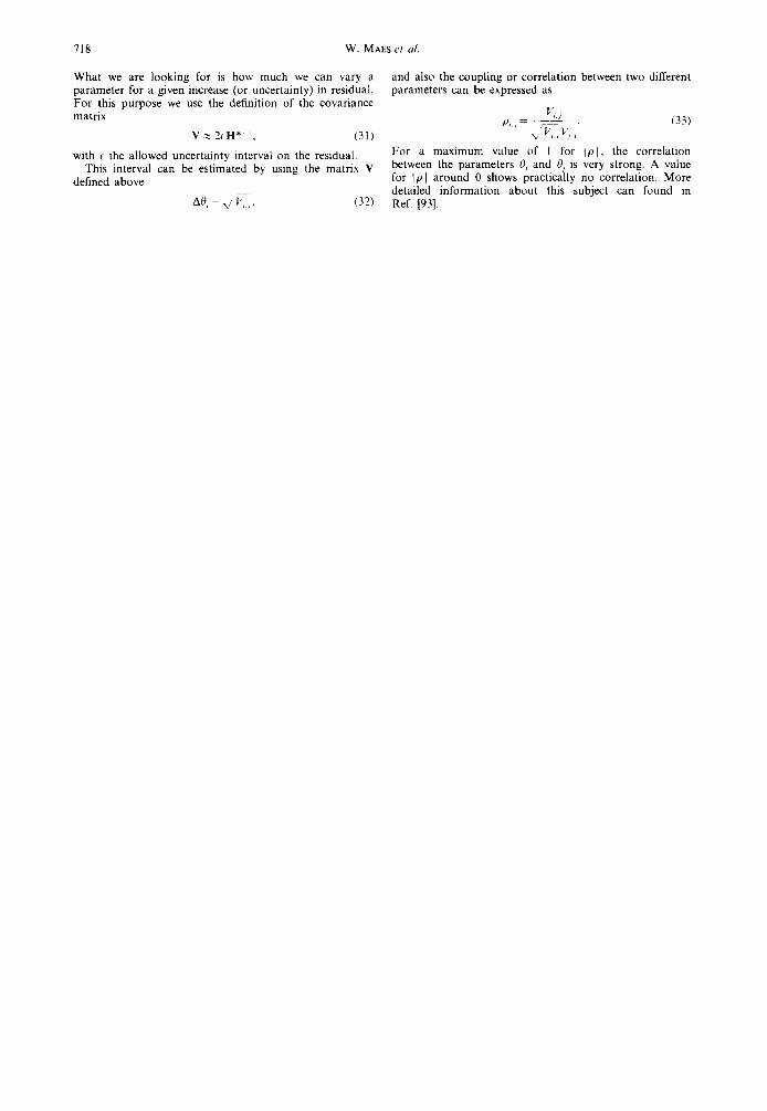
What we are looking for is how much we can vary a parameter for a given increase (or uncertainty) in residual. For this purpose we use the definition of the covariance matrix
V ~ 2~H* i (31)
with ~ the allowed uncertainty interval on the residual. This interval can be estimated by using the matrix V
defined above
A0, = ,j" V, ... (32)
and also the coupling or correlation between two different parameters can be expressed as
V,.j P,,~- . (33)
/ V , I / , \ : , .
For a max imum value of 1 for I Pl , the correlation between the parameters 0, and 0~ is very strong. A value for IPl around 0 shows practically no correlation. More detailed information about this subject can found in Ref. [93].