ill* •ft' - NASA · BQ output voltage at start of commutation L inductance of one winding of ......
24
N A 8 A ' r T6C H MI C A i, o* t X ill* • ^ -«g«. 1 »'^», !^i . .| ii|( .1.-- Arthur (i •«« -* ; •. |s >" • t| i«r % •^ HAS* TH X-2442 •ft' • E- WITR PEOTlcf ION" S ' fi« D,. t 1911 https://ntrs.nasa.gov/search.jsp?R=19720005575 2018-07-06T16:09:05+00:00Z
Transcript of ill* •ft' - NASA · BQ output voltage at start of commutation L inductance of one winding of ......

N A 8 A 'rT 6C H MI C A i,
o*
tX
ill*
• ^ -«g«. 1 »'̂ », !^i . .| ii|( . 1 . - -
Arthur (i•«« -*; •. |s >" • t| i«r
%
•^
HAS* TH X-2442
•ft' •
E-WITR PEOTlcf ION" S '
fi«
D,. t 1911
https://ntrs.nasa.gov/search.jsp?R=19720005575 2018-07-06T16:09:05+00:00Z

1. Report No. 2. Government Accession No. 3. Recipient's Catalog
NASATMX-2442No.
4. Title and Subtitle 5. Report DateSILICON -CONTROLLED-RECTIFIER SQUARE -WAVE December 1971INVERTER WITH PROTECTION AGAINST COMMUTATION 6. Performing Organization Code
FAILURE7. Author(s) 8. Performing Organization Report No.
Arthur G. Birchenough E-652810. Work Unit No.
9. Performing Organization Name and Address 112-27
11. Contract or GrantNational Aeronautics and Space AdministrationPlmml-inr! fttiin A.llTn ... - • .
No.
13. Type of Report and Period Covered
12. Sponsoring Agency Name and Address Technical Memorandum
14. Sponsoring AgencyWashington, B.C. 20546
Code
15. Supplementary Notes
16. Abstract
The square-wave SCR inverter that was designed, built, and tested includes a circuit to turn offthe inverter in case of commutation failure. The basic power stage is a complementary impulse-commutated parallel inverter consisting of only six components. The 400-watt breadboard wastested while operating at ±28 volts, and it had a peak efficiency of 95. 5 percent at 60 hertz and91. 7 percent at 400 hertz. The voltage regulation for a fixed input was 3 percent at 60 hertz. Ananalysis of the operation and design information is included.
17. Key Words (Suggested by Author(s)) 18. Distribution Statement
SCR Inverter Unclassified - unlimitedForced commutationCommutation failure protection
19. Security Classif. (of this'report) •' ' • - - • ""20. Security Glassif'lbf this'page')^ j 21. No. of Pages
Unclassified Unclassified 22
»
*
22. Price*
$3.00
' For sale by the National Technical Information Service, Springfield, Virginia 22151

SILICON-CONTROLLED-RECTIFIER SQUARE-WAVE INVERTER
WITH PROTECTION AGAINST COMMUTATION FAILURE
by Arthur G. Birchenough
Lewis Research Center
SUMMARY
A square-wave silicon controlled rectifier inverter that was designed, built, andtested includes a circuit to turn off the inverter in case of commutation failure. Thebasic power stage is a complementary impulse-commutated parallel inverter consistingof only six components. The 400-watt breadboard was tested while operating at ±28volts, and it had a peak efficiency of 95. 5 percent at 60 hertz and 91. 7 percent at 400hertz. The voltage regulation for a fixed input was 3 percent at 60 hertz. An analysisof the operation and design information is included.
INTRODUCTION
A technique under consideration for starting dynamic space-power systems involvesusing the alternator as a motor to accelerate the rotating assembly to the speed at whichit becomes self-sustaining (refs. 1 and 2). In the 2- to 15-electrical-kilowatt (kW )Brayton space-power system under investigation at the NASA-Lewis Research Center,the inverter, which drives the alternator, is required to supply a peak output current ofnearly 200 amperes. A transistor inverter was designed and built for this application;however, because higher-current - higher-voltage silicon controlled rectifiers (SCR's)are more available, SCR-inverters are generally more practical, particularly on largersystems.
A major disadvantage of dc-ac SCR inverters, however, is the possibility that anSCR will not commutate. A commutation failure generally results in a low-impedanceshort across the dc supply. In general, the commutation circuit also requires a signif-icant number of additional parts. The inverter described in this report requires only sixparts in the power stage, including the two components required for commutation. A

modification that will turn off the inverter in case of a commutation failure, clearing theshort circuit on the input lines, is also discussed.
Current and voltage transients are inherently limited, without the use of di/dt ordv/dt snubbers, and the circuit is basically frequency and symmetry independent. A400-watt, 400-hertz, single-phase model powered from a ±28-volt source was designedand tested for this investigation.
CIRCUIT DESCRIPTION*
Power Stage Operation\
As in most square-wave inverters, this design consists primarily of a pair ofswitches, SCR1 and SCR2 (fig. 1), that alternately connect the load to opposite terminalsof the power supply. Although the center tapped inductor L and Cg form a low passfilter, they are too small to provide any substantial filtering; their function is in thecommutation of the SCR's. Figure 2 shows the ideal waveforms for one cycle of opera-tion. At tj in figure 2, SCR1 is conducting. There is a current iL in one winding ofL and in the load, and Cg is charged to nearly V+.. The commutation cycle is startedby firing SCR2, which conducts, connecting terminal 3 of L to V-. Because C ischarged to V+, there will be a voltage of 2V across the winding between terminals 2and 3 of L. The turns ratio of L is 1:1, so a voltage of 2V will be induced in the otherwinding. This reverse biases SCR2, to a voltage of -2V, turning it off. The capacitorC0 is now supplying the load current and the current that was flowing in L equal to the
o
Groundc
L 1
YSCR1 ACR3
SCR2V !CR4 ±
;cs
Figure 1. - Basic inverter power stage.

**3 ***
&-J3
<§s
•— t QJC£ OiO jS
•"8
CVJ O)
"1
(!)
Z§°1
Csj "cQl OJo tVI 3
0
sio *-3
o
l_-Sco ff2-3ro ^30 <->
2V
0
-2V
O\/tw
-2V
n\l
2V
"
'^\ / \
-
- / r- V I /i/ /
/I/
-2V L '
„o
r N N. V_ . \
2'Lr /^ " " /\i, /^^^ /L r 1 '0
1 L i
V r— ^u4iL
2'L
0
A-4iL
r
' (\ (\
I I 11 1u
H 2. 5 mssc •"h (1 cycle)
Figure 2. - Ideal waveforms.
load current IL> This current is now flowing in the winding between terminals 2 and 3 ofL through SCR2, since SCR1 is off. Capacator Cg also supplies the increasing currentin L due to the voltage across it. As CR discharges to 0, SCR1 is no longer reversebiased, but it will have regained its forward blocking ability.
When Cg charges to V-, the commutation cycle is ended, but the excess currentthat built up in L during commutation must be dissipated. This current will circulatethrough CR4 and SCR2 until the energy is dissipated in the semiconductor and I R losses.At this time SCRl can be tripped and the cycle repeated. The time scale has been dis-torted in figure 2 to show the operation more clearly. The time required for commuta-tion is 15 microseconds. It should be noted that the peak forward or reverse SCR voltageis only 2V and the dv/dt is limited by Cg. The di/dt is limited by the SCR turnoncharacteristics until the current reaches IL, and then the di/dt is limited by L. Eventhe diode stress is limited to 4V. The peak voltage, peak current, and dv/dt and di/dt

stresses are very low, and the turnoff time of the SCR, which is highly reverse biasedduring turnoff, is the only critical parameter. The load capability of the inverter is verynear the 180° conduction current rating of the SCR's.
The size of the commutation components can be found from the equation for the out-put voltage during the commutation internal, obtained in appendix A:
e(t) = 2en cos — L. - 2iT J- sin -Ju , — ^ir i
VLC ^- e
where
e(t) output voltage
BQ output voltage at start of commutation
L inductance of one winding of commutation inductor L
C capacitance of commutation capacitor Cn
i-r load current
This equation assumes that i, is constant during the commutation cycle, as with an in-ductive load, which is the worst case. Full load gives the shortest commutation time,and, since t « LC, using the approximation sin w « w and cos w.« 1 - w /2 results
in
eft) « e0 - 2iL - _ e0
To find the capacitor size, set e(t) =0, for at this time the SCR is no longer reversebiased.
2iTt .2C «_ii- + L
eO L
Using the maximum value of the SCR parameter "t off" for t gives the minimum valuefor C:
Practical values for L have only a second-order effect on C, and L is selectedfor acceptable physical size and peak SCR current.

The current in the capacitor is simply
dt
and the rms current is approximately
Ws = < Vms
where f is the output frequency. This current is less than 1 ampere for this inverterand allows the use of high-density metalized or electrolytic capacitors.
The operation of this circuit is very similar to a form of a Bedford -McMurray in-verter (refs. 3 and 4). The primary difference is the placement of the diodes. Thisplacement improves the waveshape and reduces the peak reverse voltage on the SCR's.
Turnoff Modification
As a single-phase inverter, this circuit has the disadvantage that it cannot be turnedoff under load, because turning off one SCR is accomplished by turning on the other.With no load, the circuit can be turned off by simply discontinuing the firing pulses be-cause the SCR current decreases to zero as the commutation energy is dissipated. Fora three-phase inverter with a delta-connected load, turnoff can be accomplished by dis-continuing all firing pulses to the three SCR's connected to either input bus. The loadcurrent then ceases, and the other SCR's turn off.
Single-phase turnoff can be accomplished under load with the addition of the compo-nents shown within the dashed lines of figure 3. The turnoff is initiated by firing SCR3and discontinuing all pulses to SCR1 and SCR2. The capacitor.C? is,discharged, so avoltage of 2V will be applied to the additional winding on L. This voltage is trans-formed across to the other windings, and the load SCR's will both be reverse biased andcommutate. The turns ratio from the primary (the added winding) to the total secondarymust be greater than 1:1 to reverse bias both SCR's. A ratio of 2:1 was used in this in-verter. Capacitor C7 is sized using the same equation as for Cg. When C^ charges to2V, SCR3 commutates and R« 5 discharges C,,. This circuit increases the nonrepetitive
reverse voltage across the load SCR's. Commutation failure protection is provided bysensing the failure, as described later, and firing this turnoff circuit.

Figures. -Turnoff circuit.
Commutation Energy Return
The additions of figure 4 provide a path for the commutation energy stored in L toreturn to the supply. While the commutation energy is being dissipated, there will be avoltage across L, as indicated in figure 4, equal to the forward drops of the SCR anddiode circulating the current. The voltage is reflected to the additional winding, andcommutation current will flow in the secondary through CR4 to the supply if the turnsratio is greater than
2VVSCR + VDIODE
where V is the supply voltage and Vg^p and VDIQDE are the forward voltage dropsof the semiconductors. The diode voltage and current are shown in figure 5, where t*corresponds to t- in figure 2. The current in the load SCR changes from that shown infigure 2, and the diodes in the original circuit will carry no current unless the load isinductive. This circuit was not used during performance testing. The turns ratio neces-sary to achieve satisfactory energy return reduces the maximum operating frequency be-cause the inductor discharges more slowly and induces very large reverse voltages onCR5. Also, the large number of secondary turns introduces stray capacitance effects inthe inductor.

Figure 4. - Commutation"energy return circuit.
2V Np
Figure 5. - Commutation energy return circuitwaveforms. (Np/Nj = turn ratio.)
Control Circuits
Because there are no critical timing problems in this inverter, there are almost norestrictions on the firing pulses. An SCR must not be fired while it is being commutated,or the commutation cycle may fail: The two SCR's would be on, and the supply would beshort circuited. Also, if the SCR's are fired at too high a frequency, before the commu-tation energy is removed from the inductor, the inductor may saturate and the inverterwill fail to commutate. The maximum frequency of this inverter was approximately 1000hertz. These restrictions are the only limits on the operating frequency of the inverter

or on the firing pulses. The timing of the firing pulses to the two SCR's need not besymmetrical if a nonsymmetrical output is desired; pulsing a SCR while in conductionnormally has no effect, so the pulses need not be alternated. It is generally advisable tosupply a string of pulses to the SCR in case the SCR current has temporarily fallen belowthe holding current, as with inductive or light loads.
The control circuit used for the inverter is shown in figure 6. Operational amplifierIC1 is used as a square wave oscillator, operating at twice the inverter output frequency,followed by a buffer IC2A and a Hip-flop, IC3A. The outputs of IC3A are two 180° out-of-phase symmetrical square waves at the inverter output frequency. Inverters IC2B,IC2C, and 1C2D form a second oscillator that generates 5-microsecond pulses at a 50-microsecond repetition rate. This oscillator is gated on during the first half of eachcycle by IC1. These pulses and the flip-flop outputs are NANDed together in IC4A andIC4B to produce the SCR drive pulses.
Figure 6. - Control circuit.
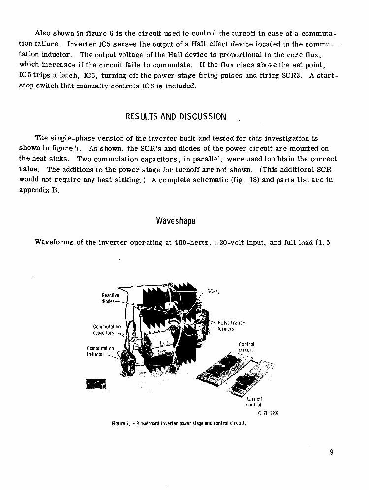
Also shown in figure 6 is the circuit used to control the turnoff in case of a commuta-tion failure. Inverter IC5 senses the output of a Hall effect device located in the commu-tation inductor. The output voltage of the Hall device is proportional to the core flux,which increases if the circuit fails to commutate. If the flux rises above the set point,IC5 trips a latch, ICG, turning off the power stage firing pulses and firing SCR3. A start-stop switch that manually controls IC6 is included.
RESULTS AND DISCUSSION
The single-phase version of the inverter built and tested for this investigation isshown in figure 7. As shown, the SCR's and diodes of the power circuit are mounted onthe heat sinks. Two commutation capacitors, in parallel, were used to obtain the correctvalue. The additions to the power stage for turnoff are not shown. (This additional SCRwould not require any heat sinking.) A complete schematic (fig. 18) and parts list are inappendix B.
Waveshape
Waveforms of the inverter operating at 400-hertz, ±30-volt input, and full load (1. 5
Reactivediodes—.—i
—SCR's
Turnoffcontrol
C-71-1702
Figure 7. - Breadboard inverter power stage and control circuit.

ohms with a small series inductive component) are shown in figures 8 to 12. The outputvoltage (fig. 8) shows a slight ringing at each switching. This ringing is reflected in thevoltage and can be reduced with an input filter. The voltage change approximately half-way through each half-cycle indicates the end of the commutation energy dissipationcycle.
The SCR voltage is shown in figure 9, and an expanded time picture of the commuta-tion spike in figure 10. The peak voltage from these figures is approximately twice thesupply voltage, and the maximum dv/dt is about 4 volts per microsecond.
The SCR current shown in figure 11 shows a large spike during the recovery time ofthe SCR being commutated and the current decay as the commutation energy is dissipated.
Figure 8. - Inverter output voltage.
Figure 9. - SCR anode voltage.
10

Figure 10. - SCR anode voltage during commutation.
Figure 11. - SCR anode current.
The SCR current at turn-on is shown in figure 12. The current, limited by the SCR turn-on time characteristics, rises almost instantly to the load current, and then increases byapproximately 1 ampere per microsecond. The SCR-limited current rise to approxi-mately the rms rating of the SCR is within the di/dt rating of most inverter SCR's.
Efficiency
The efficiency of the inverter was measured at 400, 200, and 60 hertz and over asupply voltage range of ±15 to ±30 volts. The load was resistive, although the wattmeter
11

Figure 12. - SCR anode current at turn-on.
added a slight inductive component. The power factor was approximately 0. 9 at theworst case of 400 hertz full load. Figure 13(a) shows the efficiency at 400 hertz for vary-ing load and input voltage. The efficiency was nearly independent of voltage for a fixedload impedance because the power output and the major loss (commutation energy) areboth proportional to the input voltage squared. Figure 13(b) shows the effect of frequencyon the efficiency. Commutation energy is constant each cycle and is therefore propor-tional to frequency and independent of load. Since the commutation energy is a majorloss, the efficiency decreases at low output powers and higher frequency. The peakmeasured efficiency was 95. 5 percent at 60 hertz for a 294-watt output and 91. 7 percentat 400 hertz for a 415-watt output.
The power loss for the same conditions is shown in figure 14. The total loss islower at light loading than at no load because some of the commutation energy is deliv-ered to the load. At 60 hertz, this effect has disappeared because commutation energy isno longer the major loss. The loss curves become asymptotic to a line through the originat high powers, which indicates that the major loss is the constant voltage drop of theSCR's. Higher voltage inverters would then tend to be more efficient (see fig. 13) be-cause the SCR drop would be almost constant.
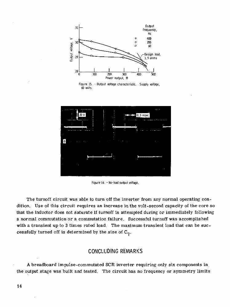
The output voltage is proportional to the supply voltage and drops with load (fig. 15).At no load, the output voltage is completely flat as shown in figure 16. With a load, thevoltage drop of the SCR produces the notch approximately halfway through each half cycle(see fig. 8). At 60 hertz, the loading effect of the wattmeter was great enough to gener-ate this notch, which accounted for the lower no-load output voltage at 60 hertz. Theregulation from no load to full load at 60 hertz and ±30 volts input was 3 percent.
12

100
90
80
70
rDesign load = 1.5 ohnv\\ .'" \
, /'-Constant load/ impedance lines
Supply voltage,• V
o 60o 50o 40* 30
(a) Output frequency, 400 hertz.
.2 lOOr
9 0 -
80-
70L
Design load = 1.5 ohm-*Output frequency,
Hz40020060
J100 200 300
Power output, W400 500
(b) Supply voltage, 50 volts.
Figure 13. - Inverter efficiency characteristics.
,r- Design load = 1.5 Supplyvoltage,
V
(a) Output frequency, 400 hertz.
Design load = 1.5 ohms-i,
Outputfrequency,
Hz
100 200 300Power output, W
400 500
(b) Supply voltage, 60 volts.
Figure 14. - Inverter power dissapation.
13
31 - Outputfrequency,
Hz
Design load,5 ohms
200 300Power output, W
Figure 15. - Output voltage characteristic. Supply voltage,60 volts.
Figure 16. - No-load output voltage.
The turnoff circuit was able to turn off the inverter from any normal operating con-dition. Use of this circuit requires an increase in the volt-second capacity of the core sothat the inductor does not saturate if turnoff is attempted during or immediately followinga normal commutation or a commutation failure. Successful turnoff was accomplishedwith a transient up to 3 times rated load. The maximum transient load that can be suc-cessfully turned off is determined by the size of C«.
CONCLUDING REMARKS
A breadboard impulse-commutated SCR inverter requiring only six components in,the output stage was built and tested. The circuit has no frequency or symmetry limits
14

except a minimum pulse width, which also limits the maximum frequency to approxi-mately 1000 hertz.
With the addition of a turnoff circuit and a flux or overcurrent detector, overloads orother conditions producing a commutation failure result in only a turnoff of the inverterinstead of an input-bus short.
The components are operated at very low peak voltages, currents, and low rates ofrise of voltage and current, dv/dt and di/dt without the use of snubbers. Also, themaximum load current rating of the inverter is approximately the 180° conduction ratingof the SCR's.
The 400-watt test inverter was operated over a range of frequency from 60 to 400hertz with input voltages from ±15 to ±30 volts. The peak efficiency was 95. 5 percent.
Lewis Research Center,National Aeronautics and Space Administration,
Cleveland, Ohio, September 29, 1971,112-27.
15

APPENDIX A
The equations describing the commutation internal are based on these assumptions:(1) The elements are ideal and lossless.(2) The output voltage efi just before commutation is equal to V the supply voltage.(3) The load current IL is constant during the commutation interval.
This is the worst case and approximates an inductive load. The equivalent circuit usedfor the analysis is shown in figure 17
ZL et
Figure 17. - Equivalent circuit.
where L is one winding of the commutation inductor, V is the supply voltage, C is thecommutation capacitor, and ZL and iL are the load impedance and current.
i, + io + IT =0 (1)
e(t) + V = L —idt
(2)
e(t) = i2dt (3)
eQ = V (assumption (2))
16
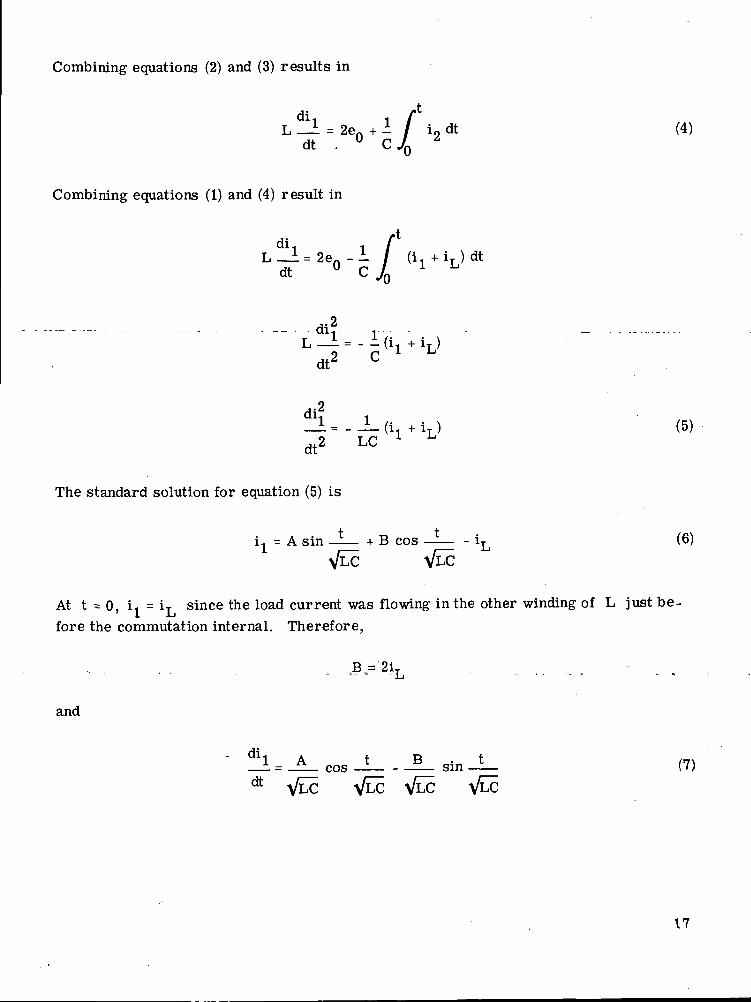
Combining equations (2) and (3) results in
L _I = 2en + ± I i, dt (4)dt . ° CJn
2
Combining equations (1) and (4) result in
ftL (i1 + iL) dtV' ./n
dijL -1 = - I (ij + iL)x
dl1 1_! = - _L a + u) (5)dt2 LC l
The standard solution for equation (5) is
ij = A sin * + B cos — IL (6)VLC >^LC
At t = 0, ij = IT since the load current was flowing in the other winding of L just be-fore the commutation internal. Therefore,
and
(7)
VLC VLC VLC
17

From equations (2) and (7)
di,
dt
2e,_0 AL -"v^t=0
A = 2eQJ~
i., = 2en /- sin t + 2iT cos — iTU I/ T I JU I i-J
(8)
From equations (1) and (3)
e(t) = i , )d t
Substituting i1 from equation (8) and integrating result in
e(t) = 2en cos — - -- 2iT J- sin —u . — -^ T r /VLC c
e
18

APPENDIX B
PARTS LIST AND SCHEMATIC
Part
R1R2R3
R4
R5)R7R6'R8R9'R10'R13Rll
R12
R14
R15
Cl
C2
C3
C4
C5C6
c7
C8
47 K
33 K
8. 2K
180
I K
. 15 K
1 K potentiometer
220, 1 W
150 K
IK, 1 W
0.05
10 pF
0.005
0.47
0. 0005
0.01
110 juF
20 jjF
Part
IC1
1C 2
1C 3
IC4,IC6
1C 5
- CR1,CR2
CR3,CR4
SCR1.SCR2
SCR3
T1'T2'T3L
Hl
jjA 748
MC672
MC663
MC679
LM311D
IN459
IN3891
C40A
C30D
1:1 ratio pulse transformer
Commutation inductorAL-8 core, 20 -mil gapwinding 1-2, 12 turnswinding 2-3, 12 turnswinding 4-5, 6 turns
Hall effect deviceH. W. Bell BH-700
19

HH"
-M-
-t>t
CJ-M-
-ot
.Si13
20

REFERENCES
1. Gilbert, L. J. ; Curreri, J. S.; and Cantoni, D. A. : Motor Starting Techniques forthe 2- to 15-kW Brayton Space Power System. NASA TM X-67819, 1971.
2. Repas, David S.; and Frye, Robert J. : Motor-Starting Characteristics of a ModifiedLund ell Alternator. NASA TM X-2200, 1971.
3. Bedford, B. D. ; and Hoft, R. G. : Principles of Inverter Circuits.John Wiley & Sons, Inc. , 1964.
4. Gentry, F. E. ; Gutzwiller, F. W. ; Holonyak, Nick, Jr.; and Von Zastrow, E. E. :Semiconductor Controlled Rectifiers: Principles and Application of p-n-p-n Devices.Prentice-Hall, Inc. , 1964.
NASA-Langley, 1971 10 E-6528