iGrafx Designer 1 - CCDA Octalglass-ware.com/User_Guides/CCDA Octal.pdf · GlassWare Audio Design...
20
Stereo Octal PCB USER GUIDE Introduction Overview Schematics Recommended Configurations Tube Lists Assembly Instructions June 30 2012 Constant-Current-Draw Amplifier Revision A
Transcript of iGrafx Designer 1 - CCDA Octalglass-ware.com/User_Guides/CCDA Octal.pdf · GlassWare Audio Design...

Stereo Octal PCB
USER GUIDE
IntroductionOverviewSchematicsRecommended ConfigurationsTube ListsAssembly Instructions
June 30 2012
Constant-Current-Draw Amplifier
Revision A

DANGER!This PCB holds a high-voltage power supply; thus, a real—and possibly—lethal shock hazard exists.
Ideally, a variac should be used to slowly power up theregulator, as it is better to have a mis-oriented electrolyticcapacitor or a mis-located resistor blow at low voltages,rather than at high voltages. Remember that the dangerincreases by the square of the voltage; for example, 200volts is four times more dangerous than 100 volts and 400volts is sixteen times more dangerous.
Once the power supply is powered up, be cautious at alltimes. In fact, even when the power supply is disconnectedor shut down, assume that power-supply capacitors will haveretained their charge and, thus, can still shock. If you are notan experienced electrical practitioner, before attaching thetransformer windings to the board, have someone who iswell-experienced in electronics review your work.
There are too few tube-loving solder slingers left; we cannotafford to lose any more.
AUDIO DESIGNwww.glass-ware.com
www.tubecad.com
Copyright © 2009-2012All Rights Reserved
GlassWare

GlassWare Audio Design
Warning!This PCB contai ns a high-voltage power supply; thus, a real and lethal shock hazardexists. Once the power transformer is attached, be cautious at all t imes. In fact, alwaysassume that the high voltage capacitors will have retained their charge even after thepower supply has been discon nected or shut down. If you are not an experiencedelectri cal practitioner, before applying the AC voltage have someone who isexperi enced review your work. There are too few tube-loving solder slingers left; wecannot afford to lose any more.
CCDA Octal PCB OverviewThank you for your purchase of the GlassWare CCDA octal stereo PCB. This FR-4PCB is extra thick, 0.094 inches (inserting and pulling tubes from their sockets won’tbend or break this board), double-sided, with plated-through heavy 2oz copper traces.In addition, the PCB is lovingly and expensively made in the USA. The boards are 6by 6 inches, with fi ve mounting holes, which helps to prevent excessive PCB bendingwhile i nserting and pulli ng tubes from their sockets.
Each PCB holds two CCDA (constant-current-draw amplifier) line-stage amplifiers;thus, one board is all that is needed for stereo unbalanced use (or one board for onechannel of balanced line-stage amplification). By including the necessary componentsfor the heater and high voltage B+ power supplies on the PCB, the CCDA boardmakes bui ldi ng a standard-setting line stage amplifi er a breeze. This assembled boardwith a chassis, volume control, selector switch, power transformer, and a fi stful ofRCA jacks is all that is needed.
PCB FeaturesB+ and Heater Power Supplies On the CCDA board, two power supplies resi de,one for the high-voltage B+ for the tubes and a low-voltage power supply for theheaters. The hi gh-voltage power supply uses an RC filter to smooth away ripple, whilethe low-voltage power supply uses a voltage regulator to provide a stable and noi se-freevoltage output. The heater regulator is adjustable and can be set to 6V or 12V. Thepower supplies require an external power transformer(s) with two secondary windin gs(120Vac to 260Vac and 12Vac to 12.6Vac).
Rev. A ImprovementsDual Coupling Capacitors The boards hold two coupling capaci tors, each findingits own 1M resistor to ground. Why? The idea here is that you can select (via a rotaryswitch) between C1 or C2 or both capacitors in parallel. Why again? One couplingcapacitor can be Teflon and the other oil or polypropylene or bee’s wax or wet-slugtantalum…. As they used to sing in a candy bar commercial: “Sometimes you feel likea nut; sometimes you don't.”
Enhanced Power Supplies The Rev. A board now has an upgraded B+ and heaterpower supplies. The B+ power supply holds an additional RC filter and the heaterpower supply can be confi gured wi th three different rectifier topologi es, includi ng avoltage doubler configuration that allows a 6.3Vac winding to run a 12V regulator.

GlassWare Audio Design
The Constant-Current-Draw Amplifier is a compound circui t that holds a grounded-cathode ampli fier directly cascaded into a cathode follower. So what; what’s so specialabout this obvious pairing? Its special status lies in the details. Each triode sees thesame cathode to plate voltage and the same load resistance and same idle currentdraw. Each sees the same signal voltage swings. Both grounded-cathode ampl ifier andthe cathode fol lower are in voltage phase, but not current phase. For example, as thegrounded-cathode amplifier sees a positive going input signal, its plate currentincreases, which increases the voltage developed across the plate resistor, which in turnswings the plate voltage down. This downward voltage swing is then cascaded into thegrid of the cathode fol lower, which decreases the plate current to the same degree thatthe previous stage's current increased. This results in the constant current draw featureof thi s topology (a highly desirable feature, as the signal ampli fication wil l not alterthe amount of current being sourced from the power supply and consequently notperturb the power supply, thus greatly simplifying the design consideration of thepower supply).
Introduction to the CCDA Circuit
A l ine stage i s needed either to boast a weak signal voltage sufficient to drive a poweramplifier to full output, or to deliver current suffi cient to drive a high capacitanceload (such as long stretches of interconnect). Just how much gain is needed for a lineamplifier? Let's begin the answer with the observation that most line amplifi ers havetoo much gain. While this extra gain impresses the audio neophyte who marvels atthe power implicit in the distorted thunder that a mere one quarter twist of thevolume knob provokes, it ultimately only subtracts from the useful range of turn onthe volume and usual ly only worsens the signal -to-noise ratio of the line stage. If 20 to30 dB of gain is too much, how much then is best? The answer wil l depend on eachsystem. A safe guess, however, would be 10 to 20 dB of gain, which translates into 3 to10 times the input signal. Calculating the gain from a CCDA amplifier i s easy, whenthe cathode resistor i s left un-bypassed, as the gain roughly equal s half the mu of theinput triode used. For example, a 6SN7 presents a mu of 20, so the gain will equal 10(+20dB). The gain from a simple grounded-cathode ampli fier , with a bypassed cathoderesistor, is a bi t more complicate:
Gain = muRa / (rp + Ra).
For example, given a 6SN7 loaded by a 20k plate resistor and whose cathode resistoris capaci tor bypassed, the gain will roughly equal 14 (+23dB).
Rload1M
1µF
Rload
Rk1M
in out
B+
B+2
CCDA Topology
GlassWare Audio Design
CCDA PCB Obviously, on this PCB many more components have been added tothe basic CCDA circuit . R3 and R5 are grid-stopper resistors and are essential ,particularly for the cathode follower output stage. The added diode is also essential ,as it protects the second triode at startup, when the cathodes are cold and thecathode follower’s cathode sits at 0V and its grid sees the full B+ voltage—never agood idea, as the cathode can see portions of i ts surface ripped away by the hugevoltage differential. C2 and C3 are cathode-bypass capacitors, which if used will bothincrease the grounded-cathode amplifier’s signal gain and improve its PSRR figure,but at the cost of increased distortion. C1 is the output coupl ing capacitor and C15its small bypass capacitor. C4 and C5 are power supply fi ltering capacitors which,with resistor R9, define a simple RC filter. R7 (the extra cathode resistor) is optional,al though highly recommended, as it buffers the cathode fol lower’s output fromheavi ly-capacitive loads and it increases the cathode follower’s linearity, but at thecost of increased output impedance.
Super low output impedance is essential, isn't it? In order to avoid insertion lossand frequency droop, a low output impedance is absolutely necessary isn't it? Well, itdepends. Consider that cheap OpAmps such as the LM741 have amazingly lowoutput impedances because of the high feedback ratios they run; yet they can't drivelow impedance loads because they are output current limited. Yet a discrete transistorline amplifier—with higher output impedance (because of less feedback) and a greateroutput current capability—may drive the same low impedance load extremely well. Sowhich was the more crucial factor: low output impedance or high current output?
Of course, if the power amplifier presents an extremely-low load impedance, a lowoutput impedance will be needed just to preserve signal level, but not necessarily topreserve bandwidth, as any cable capacitance would effectively be cou ntervailed bythe load's own low impedance. No, the real threat to bandwidth comes from highimpedance loads, which are bogged down by the h igh capacitance (because of longinterconnects and the power amplifier’s own input capacitance); and when thiscapacitance cannot be charged and discharged quickly enough, poor bandwidthresults. The key words in the previous sentence were "charged" and "discharged."Charging a capacitor quickly requires current . The quicker the charging, the greaterthe current flow. The formula is a simple one: Current =Slew Rate x Capacitance or
I = SR x C,
where slew rate refers to the amount of voltage that must be developed within acertain amount of time. Therefore, in order to guarantee wide bandwidth, the linestage must be capable of delivering a fairly high current at i ts output.
Isn't phase inversion bad? The CCDA inverts the signal polarity and phaseinversion to be avoided at all costs...right? No, unless you can 't reverse thepositive/negative connections of the speaker cable to the power amplifier. Line stagephase inversion just needs a screwdriver to fix. If the line amplifier inverts the phaseand the power amplifier doesn't, then invert the speaker's phase. If the line amplifierinverts the phase and the power amplifier also inverts, then don't invert the speaker'sphase.

GlassWare Audio Design
Unlike the Aikido, which delivers a perfect platform for tube rol ling, as vastlydi fferent tubes can be swapped in and out of the board (6BL7 or 6SL7) withouthaving to change the resi stor values, the CCDA requires more care in selectingresistor values. For example, a 6SN7-based CCDA line-stage ampli fier that used 20kplate and 430-ohm cathode resistors could never accept a 6SL7, 6H30Pi, or 6SN7, asthe resulting plate voltage would not center at B+/2, which the CCDA requi res. Theproblem is, assuming that even if we stick to just one tube type, the daunting array ofdi fferent possible B+ voltages. For example, a 6SN7-based line-stage amplifier mightrun a B+ voltage of only 140Vdc or as much as 300Vdc. Assuming an idle current of7.5mA per triode, a huge array of plate and cathode resi stors would be needed.Moreover, the plate resistor cannot be the li ttle 1/2W devices that the Aikido freelyuses, but big 2W (or 3W) power resistors, which are hard to find and expensive. Thesolution the problem of too many resistor combinations is to let the idle currentmove, but lock the plate and cathode resistor values. A triode with a cathode andplate resistors acts l ike a resistor , not a perfect resistor, but a fai rly good one.
As the graph above reveals, a 6SN7 triode, with an un bypassed 430-ohm cathoderesistor, behaves much like a 20k resistor. (By the way, note the much improvedlinearity over the plate curve traces, albeit at the cost of greatly increased plateresistance and reduced transcon ductance. Adding a plate resistor also makes thetriode behave more like a good resistor.) Th e formula for the effective resistance(with an unbypassed cathode resistor) is:
R = rp + Ra +(mu + 1)Rk.
The upshot is that if we ch ose plate and cathode resistors values to work at the centerof a range of possible B+ voltages, these same Ra & Rk resistor pairs will stil l split theB+ voltage across a wide range of B+ voltages. For example, with the 430-ohmcathode and 20k plate resi stors, the 6SN7's plate will fall close to the half of the B+voltage over the range of 150Vdc to 300Vdc.
0V 40V 80V 120V 160V 200V 240V 280V 320V 360V 400V
25mA
20mA
15mA
10mA
5mA
0mA

GlassWare Audio Design
What does the diode do in this circuit? This diode does not do anything during thenormal operation of the circuit. It can't; as the diode is so placed that the cathodewould have to be at some lower voltage than is the grid, which under normaloperation does not happen. The tube (being a depletion mode device) conductscurrent in spite of the grid being negative relative to the cathode, which is the basisfor cathode biasing, or as i t is sometimes call ed "auto biasing." If the grid were tobecome positive relative to the cathode, however, the diode would conduct and thegreatest voltage difference between the grid and cathode would equal the voltage dropacross the diode, which i s usual ly between 0.3 to 1.2 volts. A situation that couldhappen if the grid were driven with an excessively large input voltage or if the B+voltage were established and the tube remained too cold to emit electrons. The lattersituation is what usually happens every the ci rcuit is turned power up.
Alternate Cathode Resistor Connection For the advanced practitioner, the CDDAAll-in-One PCB accepts two ways of bypassing the grounded-cathode amplifier’scathode resistor. The first i s to use jumper J5 and capacitors C2 & C3. The secondapproach is to use jumper J4 and forgo the bypass capacitors. The fi rst configurationrequires halving the cathode resistor’s nominal value, as twice the current wi ll flowthrough the resi stor. The resistor is effectively bypassed, however, as anti -phase ACcurrent flows from the cathode follower side of the ci rcuit into the cathode resistor,effectively establishing a DC current flow and constant voltage drop across theresistor. (In real ity, a small amount of AC current signal will superimpose a smal l ACsignal across the resistor.) Just as we can wear a belt with suspenders, the bypasscapacitors can be added to this configuration. But do first try it without thecapacitors.
in½V1
½V1
J5
J4
+200V
+100V
300
1M 215
300
+102V
+2.15V
20k
20k
V1 = 6SN7/12SN7/12SX7
in½V1
½V1
J5
J4
+200V
+100V
300
1M 430
300
+102V
+2.15V
20k
20k
Positive FB Conventional
430 430
No doubt many applications do require al l the gain an d the PSRRimprovements possible, such an M C cart ridge pre-preamp or a microphonepream p; but for line-st age am plifier use, the bigger problem is usually toom uch gain , not too l ittl e. For example, a 12SX7-based CCDA line-stageam pl ifi er, with an unbypassed cathode resistor, wi ll deliver a voltage gain ofabout 10, or 20dB, which is plen ty. And the 6SL7 offers a very high mu of 70an d, thus, wi ll deliver a gain 35, or +10dB more than the 12SX7 (or 6SN7),wi th an unbypassed cathode resi stor. Be sure to try the CCDA withconfiguration on the right and without bypass capacitors fi rst.
1M 1M
+100V+100V
V1 = 6SN7/12SN7/12SX7

TUBE 1.5K 10K 20K 30K 75K 150K
6BL7 NA 360 960 NA NA NA
6BX7 NA 760 1760 NA NA NA
6H30Pi NA 530 1200 NA NA NA
6SL7 NA NA NA NA 845 1.5K
6SN7 NA NA 430 845 NA NA
12SX7 NA NA 430 760 NA NA
6082 360 NA NA NA NA NA
Rk for Plate Resistor Values
GlassWare Audio Design
Cathode Resistor ValuesThe cathode resistor and plate voltage set the idle current for the triode: the larger thevalue of the resistor, less current; the higher the plate voltage, more current. In general,high-mu triodes require high-value cathode resistors (1-2K) and low-mu triodes requirelow-valued cathode resistors (100-1k). The formula for setting the Iq is both simple andfairly accurate:
Iq = B+ / (Ra + rp + [mu + 1]Rk)
So, for example, a 6SN7 in a CCDA with a B+ voltage of +300V and 860 cathoderesistors will draw 300/(30k + 6.5k + [2 + 1]860) amperes of current, or about 5.5mA.But in the CCDA, the input triode’s cathode resistor must do more than just set the idlecurrent: it must also set the plate voltage to half that of the B+ voltage. So we mustwork backwards from the B+ voltage and the plate resistor’s value to zero in on thecorrect cathode resistor value. For example, assuming a 6SN7 triode and final B+voltage of 250Vdc and a plate resistor value of 20k, we know that half the B+ is equalto 125Vdc, which divvied by the 20k plate resistor equals an idle current equal to6.25mA.
Now, we must find the cathode resistor value that will ensure the halving of the B+voltage. Fortunately, a simple formula gets us close:
Rk = (Ra - rp) / (mu + 1)
Thus, in this example, using the tube manual’s specifications of a mu of 20 and an rp of6.5k, Rk should equal 643 ohms. In fact this resistor will result in too little current beingdrawn, resulting in a plate voltage 15V too high; and the empirically derived value iscloser to 430 ohms. Refer to chart below for many more illustrations.
Rk
B+
R'
B+
=
The above values are with jumper J5 in place. If positive feedback is used (J4),then half the above cathode resistor values.

GlassWare Audio Design
C4 =C5 =
C7, C8 =C17 =
C19-22 =
0.1µf to 1µF* (0.68µF 400V)47µF to 470µF* (150µF 400V or 270µF 200V)47µF to 300µF* (47µF 450V or 220µF 200V)0.01µF to 0.47µF >= 100V1000pF to 0.01µF 1kV
*Voltage depends on transformer used.All must exceed the B+ voltage.
() Parentheses denote recommended valuesTypical Part Values
AC
R13R14
R15 R16C7
B+test-point
to Heater -
J13
C17
R9a
C5C4
R9b
C8
D1D2
D4D3
C19
C22C21
C20
R17
CT
R18
R19
R18
to right channel B+
to left channel's R9
Chassis
HER108, 1N4007, UF4007
100 to 20k10-ohm 1W100-1K300k 1W100k 1W
D1-4 =
R9(a & b) =R13-16 =
R17 =R18 =R19 =
to left B+
B-Plus Power SupplyThe high voltage B-plus power supply resides on the CCDA PCB. It contai ns a full-wave bridge rectifier circuit and reservoir capacitor, which is then followed by an RC-smoothi ng filter; then each channel gets its own RC filter. The high voltage powertransformer is external to the PCB and can be mounted i n, or outside, the chassis thathouses the PCB. The optimal B-plus voltage depends on the tubes used. For example,12SX7 can be used with a low 100V power supply, while a 6SN7 works better with a150V to 240V B+ voltage. The sky is not the limit here, as the power supply capacitorsand the heater-to-cathode voltage set an upward li mi t of about 350V for the powersupply voltage after the rectifi ers and about 300V at the tubes after the RC filter.
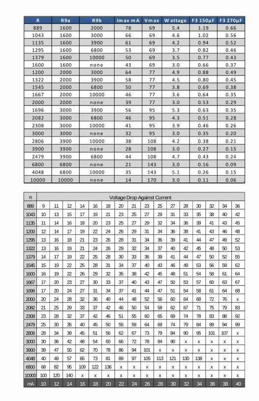
Resistors R9a & R9b are i n parallel and they define the resistor in the RC powersupply filters with capacitors C4 & C5. Resistor heat equals I² x R (and V²/R); forexample, 20mA and 5k will dissipate 2W. See page 12 and the back inside cover formore informati on. Several goals that work against each other: we want the largestvoltage-dropping resistor value possible, as it reduces the ripple CCDA’s power supplyconnection; and we want the smallest value for R9, as this resistor limits themaximum idle current that can flow through the CCDA stage; and we want the lowestraw B-plus voltage possi ble, as it will allow a larger-valued reservoi r capaci tor and limitthe heater-to-cathode voltage; and we want the highest plate voltage possible for thetubes, as it makes for better sound. We cannot have it all. Choices must be made andconsequences must be accepted. Runn ing high voltage and high current will make fora short tube life and a wonderful sound. Runn ing low voltage an d low current willgreatly extend tube life an d save money on part cost. For example, a typical 250Vcapacitor is much more volumetrically efficient and cheaper than a 400V capacitor.Thus, running a lower B-plus voltage allows us to increase greatly the total capacitancein the power supply, at a lower cost.

GlassWare Audio Design
Power Transformer(s)The CCDA PCB requires a power transformer(s) to energize i ts two power supplies.The heater power supply power transformer must offer at least 1.8 times more currentthan the heaters wi ll draw. For example, two 6SN7s wi ll draw 0.6A @12.6v, so theheater power transformer must be able to sustain an AC 1.08A current draw. Inaddition, with sine waves, the AC voltage equals the peak voltage divided by thesquare root of 2, i.e. 1.414. For example, a 10Vac sine wave peaks at 14.14V; a 6.3Vac,8.9V. In other words, a sine wave that peaks at 14.14V wil l produce the same amountof heat in a resi stance as a 10Vdc voltage source would produce across the sameresistance; thus, we label the 14.14Vpk sine wave as being 10Vac. In order to get the16Vdc raw DC voltage that a 12.6V heater voltage regulator requires an input voltageequal to remainder of 16V minus the recti fi er loss (about 2V) divided by 1.414, whichis roughly 12.6Vac.
The high vol tage power transformer must also fol low the same rules. Thus, to achieve300V of raw DC voltage, the transformer primary must deliver (300V + 2V) / 1.414,or about 214Vac. And if 50mA is required, the power transformer must be rated for50mA x 1.8 (in a full-wave bridge rectifier circui t), or 90mA. Thus, such a transformerVA rating would be rated about 20VA, as 0.9 x 214 =19.71.
Full-Wave Bridge This is the most popular power supply configuration. The entireprimary winding is used and four rectifiers are required. This configuration is seldomused with tube rectifiers, as the rectifier cathodes cannot be heated by just a singleheater winding. The two solid-state diode voltage-drops count for little in a high-voltage power supply, but are a big liability in low-voltage power supplies.
A center-tapped primary can be used as well; just leave D3, D4, R12, and R13 off theboard, then attach the center-tap to D3 or D4’s bottom eyelet, where its label appears.
Center-TappedTransformer
Iout =Vdc =
Iac / 1.27Vac* / 1.43 - Vdiode
*entire primary
Iout =Vdc =
Iac / 1.8(Vac x 1.4) - 2Vdiode
CT
AC
AC
C7
R13
R14D2
D1J13
C8
R17
AC
AC
C7
R14D2
J13
R13D1
D4
D3
R16
R15
Non-Center-TappedTransformer
C8
R17

GlassWare Audio Design
54
V1
J1
+H
-H
Heater Jumper Wire Schedule
Tubes V1 & V2If tubes are 6.3V: J2 only
If 12.6V: J1 & J3
With a 12.6V PS
V2
5 4
J2 J3
Tubes V1 & V2All tubes = 6.3V: J1 & J3
If tubes = 12.6V: Cannot be used with 6.3V PS
With a 6.3V PS
C17
AC
LD1085
Adj
InOut
Heater +
Heater -
C15
C14
R20D6
D5
D8 C10D7C9
D10 C12D9C11
R21
{
C18
+
+
+
+
AC
CTC13
C16
to B+ heaterbias voltage
Heater IssuesThe CCDA PCB holds the heater raw power supply and voltage regulator. Theregulator uses the LD1085 low-dropout adjustable voltage regulator. The regulator canbe set to an output voltage between 6V to 25V, but the assumption is that a 12Vdcoutput voltage will be used for the heaters, so that 6.3V heater tubes (like the 6SN7and 6SL7) or 12.6V tubes (like the 12SN7 or 12SX7) can be used. One heater-voltagetype tube must be used exclusively. In other words, do not use a 12SN7 and a 6SN7at the same time.
The preferred power supply voltage is 12V, even wi th four 6.3V tubes; 12V greatlyunloads the regulator and increases the dropout threshold. A 6Vdc (or 6.3Vdc) heaterpower supply can be setup, as long as all the tubes used have 6.3V heaters (or a 5V or8V or 18V power supply can be used, if all the tubes share the same 5V or 8V or 18Vheater voltage). Note: Perfectly good tubes with uncommon heater voltages, such asthe 8SN7, can often be found at swap meets, eBay, and surplus stores for a few dollarseach. Think outside 6.3V box. To place the two tube heater elements in seri es, usejumper J2; in parallel, J1 & J3.
AC Heaters An AC heater power supply (6.3V or 12.6V) can be used, if the heaterrectifiers, power supply capacitors, and regulator are all left off the board. This is notin the least recommended, as the hi gh-current AC voltage will introduce hum andcompromi se the bass reproduction.

GlassWare Audio Design
The target reference voltage for the heater’s power supply is one quarter of the B-plusvoltage that the CCDAs tubes see, not the initial raw B-plus voltage at C6.Alternatively, you might experiment with floating the heater power supply, by“grounding” the heater power supply via only a 0.1µF film or ceramic capacitor,leaving resistors R18 and R19 off the board. The capacitor will charge up through theleakage current between heater and cathodes. Not only is this method cheap, it is oftenquite effective in reducing hum with certain tubes.
Since one triode’s cathode sits close to ground potential and the other close to half theB+ voltage, the heater-to-cathode voltage experienced differs between triodes. Thesafest path is to reference the heater power supply to a voltage equal to one fourth theB+ voltage that appears after resistor R9; for example, 75V, when using a final 300VB+ voltage. The ¼ B+ voltage ensures that both top and bottom triodes see the samemagnitude of heater-to-cathode voltage. The easiest way to set this voltage relationshipup is the following circuit:
Heater Voltage =
R16 =R17 =
D5 - D8 =D1, 2, 9, 10 =
C8 - C9 =C12 =
C13, C14 =C17 =
Regulator =Vac Input =
6V 6.3V 8V 12V 12.6V
470 499 670 1.07k 1.13k124 same same same same
MUR410G " " " "1N4007 " " " "
0.01µF - 50V " " " "10kµF - 16V " " " "1kµF - 16V " " " "3900µF - 16v " " " "
LD1085, LM317, LM350, LT10857-8Vac @ 5A for 6.3Vdc12-12.6Vac @ 2.5A for 12Vdc or 12.6Vdc
Typical Part Values
Resi stors R16 and R17 set the heater voltage regulator’s output voltage. The formulais
For example, using a 125-ohm resi stor for R17 and a 1.07k resistor in R16 posi tion,the output will climb to 12Vdc. See the values table above.
V0 = 1.25(1 + R16 / R17)
DCHeater
Regulator
300k1W
47k1W
0.1µF250V
ACR19
R18
Final B+4
R9
C5C4
Raw B+Right B+Left B+
R19300k1W

GlassWare Audio Design
Adj
InOut
Heater+
AAC
C
Regulator
Adj
InOut
AAC
C
Regulator
Heater-
Heater+
Heater-
Capacitor C13 & C14 positive leads pointing to heatsinkFullwave-Bridge Rectification. Raw DC voltage = 1.414Vac - 2V
Capacitor C13 & C14 positive leads pointing to the "CT" padFullwave-Volatge-Doubler Rectification. Raw DC voltage = 2.828Vac - 2V
CT
CT
Voltage Doubler
Full-Wave Bridge
Adj
InOut
Heater+
AAC
C
Regulator
Heater-
CT
Capacitor C13 & C14 positive leads pointing to heatsinkFull-Wave CT Raw DC voltage = 1.414Vac - 1V
Full-Wave Center-Tap
C14
C13
C14
C13
C14
C13
As can be seen, the power supply can accept either full-wave bri dge rectifi er circuit or afull-wave voltage doubler recti fier configuration. When used as a full-wave bridgerectifier circuit, the two power supply filtering capacitors are placed in parallel byorienti ng their positive leads to where the heatsink sits; and the secondary attaches tothe two encircled AC pads. Configured as a voltage doubler, these capacitors placed inseries by being rotated 90 degrees clockwise, so the positive leads point to the center-
tap pad at the bottom of the PCB; the secondary attaches to single AC pad in betweencapacitors C13 and C14 and AC pad that feeds rectifier D7 and D9; and D8, D10,C10, C12 are left off the PCB. If used as a full-wave center-tap circuit, the two powersupply fi ltering capacitors are placed in parallel by orientin g their positi ve leads towhere the heatsink sits; and the secondary attaches to the two encircled AC pads andthe secondary center-tap attaches to the CT pad and C11, C12, D9, and D10 removed.
D8 C10D7C9
D10 C12D9C11
D8 C10D7C9
D7C9
D9C11

GlassWare Audio Design
TV to selector switchCATV to TV
or
GroundingThe CCDA PCB holds a star ground at its center. Ideally, thi s will be the only centralground in the line-stage amplifier. Groun d loops, however, are extremely easy tointroduce. For example, if the RCA jacks are not isolated from the chassis, then thetwisted pair of wi res that connect the PCB to the jacks will each define a ground loop(as will jumper J13, which bridges the PCB’s ground to the chassis). The solution iseither to isolate the jacks or use only a single hot wire from jack to PCB (the wire canbe shielded, as long as the shield only attaches at one end). The Absolute-Stargrounding scheme has each input signal source and each output lead geting its ownground wire that attaches, ulti mately, at one star ground poin t; each RCA jack isisolated from the chassis. The CCDA PCB was designed to work with this approach,although it can be used with any approach.
House Ground The third pron g on the wall outlet attaches to the house’s ground,usually the cold water pipe. The line-stage amplifier can also attach to this groundconnection, which is certainly the safest approach, as it provides a discharge pathshould the B+ short to the chassis. Unfortunately, this setup often produces a humproblem. Some simply float the ground, others use several solid-state recti fiers inparallel to attach the chassis ground to the house ground (NOT NEUTRAL) via thethird prong, and others still use a 10-ohm resistor shunted by a small capacitor, say0.001µF to 0.1µF/250V.
HouseGround
ChassisGround
100.01µF250V
SignalGround
Chassis Ground Jumper J13 connects the PCB’s ground to the chassis through thetop leftmost mounting hole. If you wish to float the chassis or capacitor couple the
chassis to ground, then either leave jumper J13 out or replace it with a small-valuedcapacitor (0.01 to 0.1µF). Warning: if rubber O-rings are used with PCB standoffs,then the ground connection to the chassis is n ot likely to be made; in thi s case, usemetal washer in place of top rubber O-ring.
CATV Ground Attachi ng a line-stage amplifier to TV or VCR can cause huge humproblems, as the “ground” used by the connecti on CATV connection my introducehum. Isolation transformers work supremely well i n thi s application. In fact, anisolation transformer can be used on all the input signals only (one transformer perchannel is required, if it is located after, rather than before the selector switch). Or aRF transformer can be used between the TV and the CATV wall connection. Look onthe Web for more complicated solutions to the CATV hum problem.

GlassWare Audio Design
Configuring a CCDA Line AmplifierThe CCDA topology makes a good line ampli fi er, as it offers low distortion and lowoutput impedance. The following design examples are by no means exhaustive, asmany more equally “correct” configurations are possible. For example, a beefy 6BX7-based CCDA line-stage amplifier that ran the triodes under high current might provethe best solution for those planning driving long high-capacitance cables.
L-in
C1-out
½V1
½V1
R1 R2
R3
R4
R5
R6
R7
R8
C15 C3C1
C4C5
R9 (A & B)
C21
2
3
6
7
8
J5
J4
D11C2-out
R22
B+ Voltage =Heater Voltage =
R1, R8, R22 =R3, R5 =R4, R6 =
R7 =
6SN7 6H30pi 12SX7 6SL7
150V - 300V (250V) 100V - 240V (200V) 200V - 300V (250V) 200V - 300V (275V)6.3V or 12.6V 12.6V 12.6V 6.3V
100k - 1M (1M) Same Same Same100 - 1k (300) Same Same Same20k 10k 20k 150k100 100 100 100
C1 =C2 =C3 =C4 =C5 =
C15 =
0.1 - 10µF* Film or PIO Same Same Same" " " "0.01 - 0.1µF Optional " " "0.1 - 1µF* Film or Pio " " "150µF/400V " " "100 - 1kµF/16V Optional " " "
*Voltage rating must equal or exceed B+ voltage
430 530 560 1.5k10 7 10 35+20dB +17dB +20dB +30dB
200 270 270 75015 12.5 15 50+23dB +22dB +23dB +34dB
400 ohm 210 ohm 400 ohm 690
300 ohm 110 ohm 300 ohm 590 ohm
Typical Part Values () Parentheses denote recommended values
Tube =
R2 with J5
R2 with J4
With R7
With R7 replaced by jumper
R2 =Gain =
Gain dB =
R2 =Gain =
Gain dB =
Zo =
Zo =

GlassWare Audio Design
Tube SelectionThe CCDA is quite flexible, as a CCDA can be built using many different tubes. Forline-stage amplifiers, the 6SN7 and 12SX7 are the obvious choices, but other twin -triodes can be used. For example, a 6SL7 input tube wil l yield a gain close to 35(mu/2), which would be suitable as the frontend of a single-ended amplifier; a 6SN7(5692) or 12SX7 input tube will yield a gain near 10, which would be excellent for aline stage amplifier; and the 6BX7 or 6H30Pi would deliver a low output impedancethat could drive capacitance-laden cables or even high-impedance headphones. The listof possible tubes is not overly long: 2C50, 6BL7, 6BX7, 6H30Pi, 6SL7, 6SN7, 6SU7,12SL7, 12SN7, 12SX7, 5691, 5692, 6082, ECC32, ECC33.
The on ly stipulations are that the two triodes within the envelope be similar and thatthe tube conforms to the 8BD base pin-out. Do try to th ink outside the 6 and 12 volttube box. For example, NOS 6SN7s sell for about $$$, but the same tubes with an 8Vor 12V heater can be bought for less than $10.
RFIRadio frequency interference can be a hassle to track down and eliminate. First makesure that the source of the problem actually resides in the line-stage amplifier. Forexample, if only one signal source suffers from RFI noise, make sure that it isnormal ly RFI free. In other words, attach it to another line-stage amplifier and see ifthe RFI persists. If it does pass this test, then try soldering small capacitors, say 100pF,from this signal source’s RCA jacks to the chassis, as close as possible to the jacks: if itfails, fix the source. Ferrite beads can also help; try using beads on the hot lead as itleaves the RCA jack and then again at the selector switch. Increasing the grid-stopperresistor’s (R3) value, say to 1k, can also work wonders (use a carbon-composition orbulk-foil resistor or some other non-inductive resistor type).
RCA Jack Terminating ResistorsHere’s a cheap trick to try: at each input RCA jack, place a 100k to 1M resistor,bridging input hot and jack ground. Why? The resistor provides a path for the ACsignal present at the jack, so given a choice between radiating into the chassis or goingthrough the relatively low-impedance resistor, the AC signal chooses the latter path ,reducing crosstalk.
Coupling-Capacitor ValuesThe bigger in value the coupling capacitor, the lower the -3dB high-pass cornerfrequency will be. The formula is as follows:
Frequency = 159155/C/R
where C is in µF. For example, with a 1µF coupling capacitor and a power amplifierwith an input impedance of 47k, the corner frequency would be 3.5Hz. The higherthe load impedance, the lower the corner frequency. The coupling capacitor voltagerating must at least equal the B+ voltage, for safety’s sake. Bypass capacitor (C15) forthe coupling capacitors (C1) is optional. Many coupling capacitor benefit from theaddition of small bypass capacitors that are one tenth to one hundredth the maincoupling capacitor’s value. Do not be afraid to experiment. Try bypassing a filmcoupling capacitor with a PIO (or mica or wet-slug tantalum or Teflon) capacitor.

GlassWare Audio Design
Assembly & Testing
Assembly Cleanliness is essential. Before soldering, be sure to clean both sides thePCB with 90% to 99% isopropyl alcohol. Do not use dull-looking solder; soldershould shine. If it doesn’t, first clean away the outer oxidation with some steel woolor a copper scouring pad. If the resistor leads look in the least gray, clean away theoxidation with either steel wool or a wire sniper’s sharp edges. Admittedly, with newresistors and a fresh PCB, such metal dull ing is rare; but if the parts have sat in yourcloset for a year or two, then expect a good amount of oxidation to have developed.
First, solder all the small diodes in place, and then solder the resistors, rectifiers,capacitors, and heatsinks. Be consistent in orienting the resistors; keep all thetolerance bands on the resistor’s body at the right side as you face the resistorstraight on. This wil l pay dividends later, if you need to locate a soldered a resistor inthe wrong location. Because the board is double sided, with traces and pads on eachside, it is easier to solder the resistors from their top side. It is often easier to attachthe LD1085 (heater regulator) to its heatsink first (using the heatsink hardware kit)and then to solder both the heatsink and regulator to the PCB at once. As the PCB isso overbuilt, it is extremely difficult to remove an incorrectly placed part. Be sure toconfirm all the electrolytic capacitor orientations, as a reversed polarized capacitorcan easily vent (or even explode) when presented with high-voltage. Confirm twice,solder once.
Testing Before testing, visually inspect the PCB for breaks in symmetry between leftand right sides. Wear safety eye goggles, which is not as pantywaist a counsel as itsounds, as a venting power-supply capacitor will spray hot caustic chemicals. Make ahabit of using only one hand, with the other hand behind your back, while attachingprobes or handling high-voltage gear, as a current flow across your chest can result indeath . In addition, wear rubber-soled shoes and work in dry envi ronment.Remember, safety first , second, and last.
1. Attach only the heater power supply’s transformer winding, leaving thehigh-voltage transformer leads unattached and electrical tape shrouded, withno tubes in their sockets.
2. Use a variac and slowly bring up the AC voltage, while looking for smokeor part discoloration or bulging.
3. Measure the heater regulator’s output voltage without and with a load. Ifthe heater regulator fails to regulate, try either lowering the heater voltage atad, for example 12V instead of 12.6V, as the 0.6V difference might beenough to bring the regulator back into regulation.
4. Next, power down the heater regulator and attach the high-voltage windingsand insert the tubes in their sockets.
5. Attach the transformer to a variac and slowly bring up the AC voltage.6. Measure the voltage across ground and B-plus pads in the center of the
PCB; then measure the voltage across capacitors, C4 & C5. If the twochannels differ by more than 10Vdc, try switching tubes from one channelto the other. If the imbalance does not follow the tubes, there is a problem,probably a misplaced part.
Only after you are sure that both heater and B-plus power supplies are working well,should you attach the line-stage amplifier to a power amplifier.

GlassWare Audio Design
Let me know what you thinkIf you would like to see some new audio PCB or kit or recommend a change to anexisting product or if you need help figuring out the heater jumper settings orcathode resi stor values, drop me a l ine by e-mail to the address on the back cover(begin the subject line with either “Aikido” or “tube” or the spam fi lters are sure toeat your message).
Top Side PCB Mechanical Layout
5.5 in
6.5
in1
.5in
3.0 in
2.0 in
CouplingCapacitor
CouplingCapacitor
6.0 in
PS BypassCapacitor
PS BypassCapacitor
7.0"
2.0 in
BypassCapacitor
BypassCapacitor
0.25 in
DecouplingCapacitor
DecouplingCapacitor
R R9a R9b Im ax m A V m ax W attage F3 150µF F3 270µF
889 1600 2000 78 69 5.4 1.19 0.66
1043 1600 3000 66 69 4.6 1.02 0.56
1135 1600 3900 61 69 4.2 0.94 0.52
1295 1600 6800 53 69 3.7 0.82 0.46
1379 1600 10000 50 69 3.5 0.77 0.43
1600 1600 n o n e 43 69 3.0 0.66 0.37
1200 2000 3000 64 77 4.9 0.88 0.49
1322 2000 3900 58 77 4.5 0.80 0.45
1545 2000 6800 50 77 3.8 0.69 0.38
1667 2000 10000 46 77 3.6 0.64 0.35
2000 2000 n o n e 39 77 3.0 0.53 0.29
1696 3000 3900 56 95 5.3 0.63 0.35
2082 3000 6800 46 95 4.3 0.51 0.28
2308 3000 10000 41 95 3.9 0.46 0.26
3000 3000 n o n e 32 95 3.0 0.35 0.20
2806 3900 10000 38 108 4.2 0.38 0.21
3900 3900 n o n e 28 108 3.0 0.27 0.15
2479 3900 6800 44 108 4.7 0.43 0.24
6800 6800 n o n e 21 143 3.0 0.16 0.09
4048 6800 10000 35 143 5.1 0.26 0.15
10000 10000 n o n e 14 170 3.0 0.11 0.06
R
889 9 11 12 14 16 18 20 21 23 25 27 28 30 32 34 36
1043 10 13 15 17 19 21 23 25 27 29 31 33 35 38 40 42
1135 11 14 16 18 20 23 25 27 29 32 34 36 39 41 43 45
1200 12 14 17 19 22 24 26 29 31 34 36 38 41 43 46 48
1295 13 16 18 21 23 26 28 31 34 36 39 41 44 47 49 52
1322 13 16 19 21 24 26 29 32 34 37 40 42 45 48 50 53
1379 14 17 19 22 25 28 30 33 36 39 41 44 47 50 52 55
1545 15 19 22 25 28 31 34 37 40 43 46 49 53 56 59 62
1600 16 19 22 26 29 32 35 38 42 45 48 51 54 58 61 64
1667 17 20 23 27 30 33 37 40 43 47 50 53 57 60 63 67
1696 17 20 24 27 31 34 37 41 44 47 51 54 58 61 64 68
2000 20 24 28 32 36 40 44 48 52 56 60 64 68 72 76 x
2082 21 25 29 33 37 42 46 50 54 58 62 67 71 75 79 83
2308 23 28 32 37 42 46 51 55 60 65 69 74 78 83 88 92
2479 25 30 35 40 45 50 55 59 64 69 74 79 84 89 94 99
2806 28 34 39 45 51 56 62 67 73 79 84 90 95 101 107 x
3000 30 36 42 48 54 60 66 72 78 84 90 x x x x x
3900 39 47 55 62 70 78 86 94 101 x x x x x x x
4048 40 49 57 65 73 81 89 97 105 113 121 130 138 x x x
6800 68 82 95 109 122 136 x x x x x x x x x x
10000 100 120 140 x x x x x x x x x x x x x
mA 10 12 14 16 18 20 22 24 26 28 30 32 34 36 38 40
VoltageDropAgainst Current