
IGLOO nano Starter Kit User’s Guide
42
IGLOO nano Starter Kit User’s Guide
Transcript of IGLOO nano Starter Kit User’s Guide
IGLOO nano Starter KitUser’s Guide
IGLOO nano Starter Kit
Revision 3 2
Table of Contents
Introduction . . . . . . . . . . . . . . . . . . . . . . . . . . . . . . . . . . . . . . . . . . . . . . . . . . . . . . . . . . . . . . . . . . . . . . 3IGLOO nano Starter Kit Description . . . . . . . . . . . . . . . . . . . . . . . . . . . . . . . . . . . . . . . . . . . . . . . . . . . . . . . . . . . . . 3Board Description . . . . . . . . . . . . . . . . . . . . . . . . . . . . . . . . . . . . . . . . . . . . . . . . . . . . . . . . . . . . . . . . . . . . . . . . . . 3Kit Contents . . . . . . . . . . . . . . . . . . . . . . . . . . . . . . . . . . . . . . . . . . . . . . . . . . . . . . . . . . . . . . . . . . . . . . . . . . . . . . . 4Web-Based Resources . . . . . . . . . . . . . . . . . . . . . . . . . . . . . . . . . . . . . . . . . . . . . . . . . . . . . . . . . . . . . . . . . . . . . . 4
1 Board Components and Settings . . . . . . . . . . . . . . . . . . . . . . . . . . . . . . . . . . . . . . . . . . . . . . . . . . . . . . 7Block Diagram . . . . . . . . . . . . . . . . . . . . . . . . . . . . . . . . . . . . . . . . . . . . . . . . . . . . . . . . . . . . . . . . . . . . . . . . . . . . . 7IGLOO nano Board Stackup . . . . . . . . . . . . . . . . . . . . . . . . . . . . . . . . . . . . . . . . . . . . . . . . . . . . . . . . . . . . . . . . . . 8Jumper and Switch Settings . . . . . . . . . . . . . . . . . . . . . . . . . . . . . . . . . . . . . . . . . . . . . . . . . . . . . . . . . . . . . . . . . 10FPGA Description: AGLN250V2-VQG100 . . . . . . . . . . . . . . . . . . . . . . . . . . . . . . . . . . . . . . . . . . . . . . . . . . . . . . . 11
2 Power . . . . . . . . . . . . . . . . . . . . . . . . . . . . . . . . . . . . . . . . . . . . . . . . . . . . . . . . . . . . . . . . . . . . . . . . . . 15Power Modes . . . . . . . . . . . . . . . . . . . . . . . . . . . . . . . . . . . . . . . . . . . . . . . . . . . . . . . . . . . . . . . . . . . . . . . . . . . . . 15Battery . . . . . . . . . . . . . . . . . . . . . . . . . . . . . . . . . . . . . . . . . . . . . . . . . . . . . . . . . . . . . . . . . . . . . . . . . . . . . . . . . . 16Current Measurement . . . . . . . . . . . . . . . . . . . . . . . . . . . . . . . . . . . . . . . . . . . . . . . . . . . . . . . . . . . . . . . . . . . . . . 17
3 Operation of Board Components . . . . . . . . . . . . . . . . . . . . . . . . . . . . . . . . . . . . . . . . . . . . . . . . . . . . . 19Clock Oscillator . . . . . . . . . . . . . . . . . . . . . . . . . . . . . . . . . . . . . . . . . . . . . . . . . . . . . . . . . . . . . . . . . . . . . . . . . . . 19Reset . . . . . . . . . . . . . . . . . . . . . . . . . . . . . . . . . . . . . . . . . . . . . . . . . . . . . . . . . . . . . . . . . . . . . . . . . . . . . . . . . . . 20Flash*Freeze Switch . . . . . . . . . . . . . . . . . . . . . . . . . . . . . . . . . . . . . . . . . . . . . . . . . . . . . . . . . . . . . . . . . . . . . . . 21Push-Button Switches . . . . . . . . . . . . . . . . . . . . . . . . . . . . . . . . . . . . . . . . . . . . . . . . . . . . . . . . . . . . . . . . . . . . . . 22DIP Switches . . . . . . . . . . . . . . . . . . . . . . . . . . . . . . . . . . . . . . . . . . . . . . . . . . . . . . . . . . . . . . . . . . . . . . . . . . . . . 23User LEDs . . . . . . . . . . . . . . . . . . . . . . . . . . . . . . . . . . . . . . . . . . . . . . . . . . . . . . . . . . . . . . . . . . . . . . . . . . . . . . . 24I/O Test Pins . . . . . . . . . . . . . . . . . . . . . . . . . . . . . . . . . . . . . . . . . . . . . . . . . . . . . . . . . . . . . . . . . . . . . . . . . . . . . 24USB-to-UART Interface . . . . . . . . . . . . . . . . . . . . . . . . . . . . . . . . . . . . . . . . . . . . . . . . . . . . . . . . . . . . . . . . . . . . . 26Low-Cost Programming Stick (LCPS) . . . . . . . . . . . . . . . . . . . . . . . . . . . . . . . . . . . . . . . . . . . . . . . . . . . . . . . . . . 27
4 Programming . . . . . . . . . . . . . . . . . . . . . . . . . . . . . . . . . . . . . . . . . . . . . . . . . . . . . . . . . . . . . . . . . . . . 29
5 Board Demonstration . . . . . . . . . . . . . . . . . . . . . . . . . . . . . . . . . . . . . . . . . . . . . . . . . . . . . . . . . . . . . . 31Powering Up the Board and Running the Demo . . . . . . . . . . . . . . . . . . . . . . . . . . . . . . . . . . . . . . . . . . . . . . . . . . 31
A Resources . . . . . . . . . . . . . . . . . . . . . . . . . . . . . . . . . . . . . . . . . . . . . . . . . . . . . . . . . . . . . . . . . . . . . . 33
B List Of Changes . . . . . . . . . . . . . . . . . . . . . . . . . . . . . . . . . . . . . . . . . . . . . . . . . . . . . . . . . . . . . . . . . . 35
C Product Support . . . . . . . . . . . . . . . . . . . . . . . . . . . . . . . . . . . . . . . . . . . . . . . . . . . . . . . . . . . . . . . . . . 37Customer Service . . . . . . . . . . . . . . . . . . . . . . . . . . . . . . . . . . . . . . . . . . . . . . . . . . . . . . . . . . . . . . . . . . . . . . . . . 37Customer Technical Support Center . . . . . . . . . . . . . . . . . . . . . . . . . . . . . . . . . . . . . . . . . . . . . . . . . . . . . . . . . . . 37Technical Support . . . . . . . . . . . . . . . . . . . . . . . . . . . . . . . . . . . . . . . . . . . . . . . . . . . . . . . . . . . . . . . . . . . . . . . . . 37Website . . . . . . . . . . . . . . . . . . . . . . . . . . . . . . . . . . . . . . . . . . . . . . . . . . . . . . . . . . . . . . . . . . . . . . . . . . . . . . . . . 37Contacting the Customer Technical Support Center . . . . . . . . . . . . . . . . . . . . . . . . . . . . . . . . . . . . . . . . . . . . . . . 37ITAR Technical Support . . . . . . . . . . . . . . . . . . . . . . . . . . . . . . . . . . . . . . . . . . . . . . . . . . . . . . . . . . . . . . . . . . . . . 38Regulatory and Compliance Information . . . . . . . . . . . . . . . . . . . . . . . . . . . . . . . . . . . . . . . . . . . . . . . . . . . . . . . . 38
Index . . . . . . . . . . . . . . . . . . . . . . . . . . . . . . . . . . . . . . . . . . . . . . . . . . . . . . . . . . . . . . . . . . . . . . . . . . 39

Introduction
IGLOO nano Starter Kit Description The IGLOO® nano starter kit is a complete package that enables you to quickly evaluate IGLOO nano family and prototype your design. The kit allows you to develop simple designs using switches and LEDs; or by removing the jumpers to the switches and LEDs you can then use the board to integrate the nano device into a full system, with all user I/Os available. In both modes you can then measure power to the device and to each I/O bank to evaluate the power consumption of your design. When using the board in conjunction with Libero® System-on-Chip (SoC) power analysis tools, you will have a clear picture of application power consumption at each stage in your design. In addition, the tool suite now includes power-driven layout (PDL), which can reduce the power consumption of designs up to 30 percent. Since IGLOO nano devices are footprint-compatible with ProASIC®3 nano devices, this kit can also be used to prototype designs for ProASIC3 nano FPGAs.
Key Features• Powered by USB cable or by external power (not supplied)• Test points for measuring current consumption of the AGLN250V2-VQG100 • USB-to-UART interface for HyperTerminal on PC connected to board• All components used on the board are low power components (i.e., LEDs (2 mA), resets (A
range), and oscillator (2-3 mA))
Board DescriptionThe IGLOO nano evaluation board (Figure 1) enables you to measure power consumption (dynamic, static, and Flash*Freeze modes) with the core operating at either 1.2 V or 1.5 V. When using the board in conjunction with Microsemi’s power analysis tools, you will have a clear picture of application power consumption at each stage in your design.
Figure 1 • IGLOO nano Evaluation Board
Revision 3 3

Introduction
In addition, the Libero SoC tool suite now includes power-driven layout (PDL), which can reduce the power consumption of designs up to 30 percent.The evaluation board has a small form factor, measuring 3.2 inches by 4 inches, and supports an AGLN250 IGLOO nano device in the 14 x 14 mm VQ100 package. The evaluation board consumes less than 150 mW. All components used on the board, such as LEDs, reset (µA range), and oscillator, are low-power components. Also included on the evaluation board is a USB-to-UART interface to allow for HyperTerminal on a PC to communicate with the IGLOO nano device on the board.The right hand side of the board has a programming connector that enables the low-cost programming stick (LCPS) to be attached to the board to program the IGLOO nano AGLN250V2-VQG100 device. I/Os from the FPGA have been wired to pads on the board for debug purposes.
Kit ContentsTable 1 lists the contents of the IGLOO nano Starter Kit.
Web-Based ResourcesListed below are the documents currently published on the Microsemi SoC Products Group website. Additional documents and design examples may be added to the website in the future.
Users Guides and Tutorials IGLOO nano Starter Kit User’s Guide www.microsemi.com/soc/documents/IGLOO_nano_StarterKit_UG.pdfIGLOO nano Starter Kit Quickstart Card www.microsemi.com/soc/documents/AGLN_NANO_KIT_QS.pdfIGLOO nano Starter Kit User’s Guidewww.microsemi.com/soc/documents/IGLOO_nano_StarterKit_UG.pdfLibero IDE Quick Start Guide www.microsemi.com/soc/documents/gettingstarted_ug.pdfLibero SoC User’s Guide www.microsemi.com/soc/documents/libero_ug.pdfFlashPro User’s Guide www.microsemi.com/soc/documents/flashpro_ug.pdf
Table 1 • IGLOO nano Starter Kit Contents
Quantity Description
1 IGLOO nano Evaluation Board with AGLN250V2-VQG100
1 FlashPro3-compatible low-cost programming stick (LCPS)
2 USB 2.0 high-speed cables
1 Quickstart card
4 Revision 3
IGLOO nano Starter Kit
Libero Quickstart Tutorial Design FilesIGLOO nano VHDL Design Files www.microsemi.com/soc/documents/IGLOO_nanoz_tutorial_VHDL_Libero84sp2_revB.zipIGLOO Icicle Verilog Design Files www.microsemi.com/soc/documents/IGLOO_Icicle_tutorial_verilog_Libero84sp2_revA.zipIGLOO Icicle VHDL Design Files www.microsemi.com/soc/documents/IGLOO_Icicle_tutorial_VHDL_Libero84sp2_revA.zip
Board ReferencesIGLOO nano Starter Kit Board – Allegro PCB filewww.microsemi.com/soc/documents/IGLOO_nano_StarterKit_PCB.zipIGLOO nano Starter Kit Board – OrCAD Schematics (DSN)www.microsemi.com/soc/documents/IGLOO_nano_StarterKit_DSN.zipIGLOO nano Starter Kit Board – PDF Schematicswww.microsemi.com/soc/documents/IGLOO_nano_StarterKit_SS.pdf
Revision 3 5


1 – Board Components and Settings
This chapter describes the components and settings for the IGLOO nano Evaluation Board.
Block Diagram The IGLOO nano board Evaluation Board is shown in Figure 1-1.
Figure 1-1 • IGLOO nano Evaluation Board
Revision 3 7

Board Components and Settings
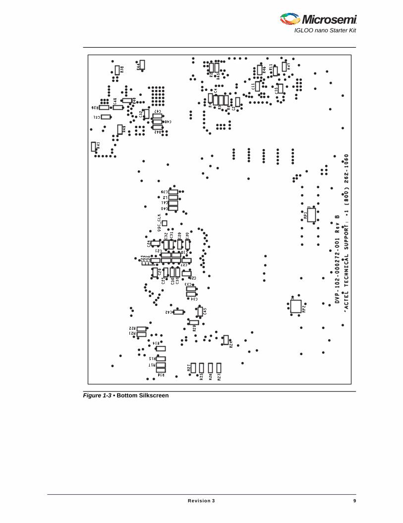
IGLOO nano Board StackupThe IGLOO nano board is built on a four-layer printed circuit board (PCB):
1. Top Signal (Figure 1-2)2. Power3. GND4. Bottom Signal (Figure 1-3 on page 9)
Figure 1-2 • Top Silkscreen
8 Revision 3
IGLOO nano Starter Kit
Figure 1-3 • Bottom Silkscreen
Revision 3 9

Board Components and Settings
Jumper and Switch SettingsRecommended default jumper settings are defined in Table 1-1. The voltage selection jumpers are highlighted in grey. Connect jumpers in the default settings described in Table 1-1 to enable the pre-programmed demo design to function correctly.
Table 1-1 • Jumper Settings for Demo Design
Jumper Default Setting Comment
JP1 Pin 2-3 Main power supply. Connect Wall/USB input to VCC_IN.
JP2 Pin 2-3 VCC CORE voltage (1.2 / 1.5 V)Pin 2-3 selects 1.2 V.Pin 1-2 selects 1.5 V. Jumper is on upper right area of board.
JP3 Pin 2-3 Current measurement header for Bank 0
JP4 Pin 2-3 Current measurement header for VCC_B2 (Bank 2)
JP5 Pin 1-2 Voltage selection for VCC B0 (Bank 0)Pin 1-2 selects 3.3 V.Pin 3-4 selects 2.5 V.Pin 5-6 selects VCC_CORE.
JP6 Pin 2-3 Current measurement header for Bank 1
JP7 Pin 2-3 Current measurement header for VCC_B3 (Bank 3)
JP8 Pin 1-2 Voltage selection for VCC B1 (Bank 1)Pin 1-2 selects 3.3 V.Pin 3-4 selects 2.5 V.Pin 5-6 selects VCC_CORE.
JP9 Pin 2-3 Current measurement header for JTAG supply.
JP10 Pin 2-3 Current measurement header for VCC (FPGA core supply).
JP11 Pin 1-2 Voltage selection for VCC JTAG (JTAG supply. Pin 1-2 selects 3.3 V.Pin 3-4 selects 2.5V.Pin 5-6 selects VCC_CORE.
JP12 Pin 2-3 Current measurement header for VCC_PUMP (FPGA charge pump supply)
JP13 Pin 1-2 Remove each short default jumper to disconnect any of the 8 LEDs from the FPGA.
JP14 Pin 1-2 Remove each short default jumper to disconnect any of the 8 DIP switches SW3.1 through SW3.8 from the FPGA.By default, SW3.1 through SW3.8 should all be closed (set to the ON settings).The 8 DIP switches are connected to the 8 LEDs (LED1, LED2, … LED8).
JP15 Pin 1-2 Remove each short default jumper to disconnect any of the four push-button switches, SW4 through SW7, from the FPGA.
SW1 OFF Flash*Freeze: To enable Flash*Freeze mode, slide SW1 toward FF_ON.In Flash*Freeze mode, current consumption of the FPGA goes below 50 µA. Current can be measured by placing a current meter between [pin1 or pin 2] and [pin 3 or pin 4] of JP10 (VCC_CORE).
10 Revision 3
IGLOO nano Starter Kit
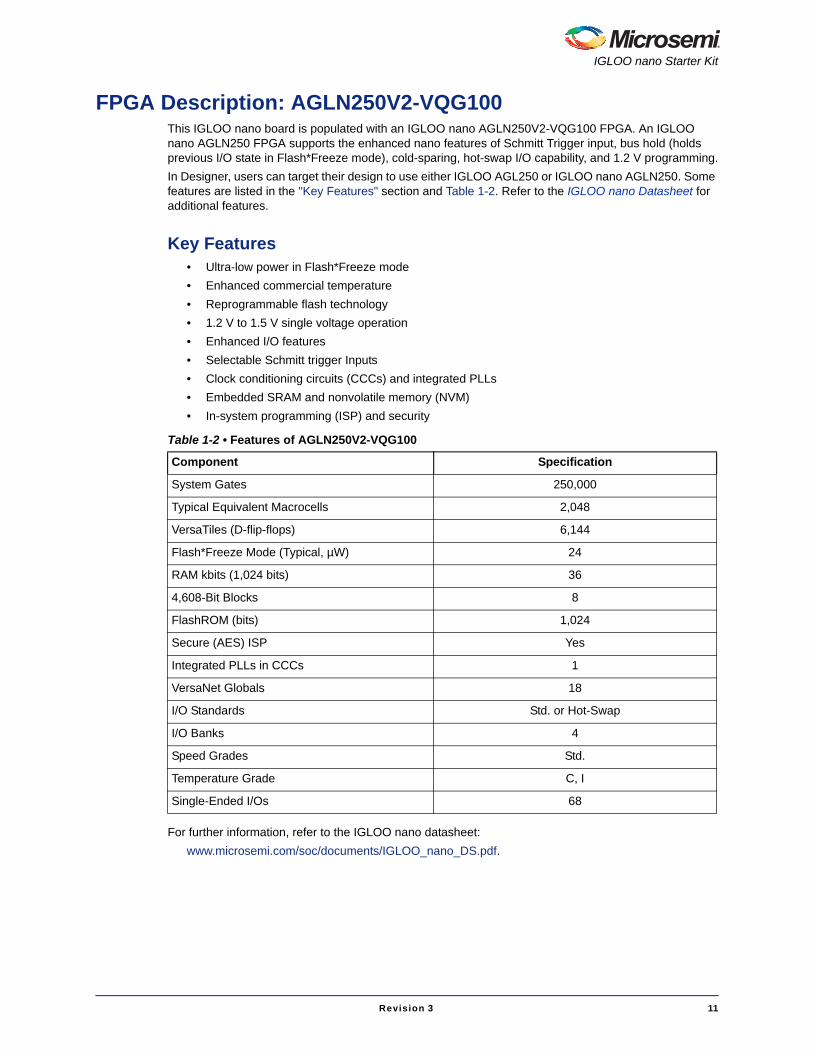
FPGA Description: AGLN250V2-VQG100This IGLOO nano board is populated with an IGLOO nano AGLN250V2-VQG100 FPGA. An IGLOO nano AGLN250 FPGA supports the enhanced nano features of Schmitt Trigger input, bus hold (holds previous I/O state in Flash*Freeze mode), cold-sparing, hot-swap I/O capability, and 1.2 V programming.In Designer, users can target their design to use either IGLOO AGL250 or IGLOO nano AGLN250. Some features are listed in the "Key Features" section and Table 1-2. Refer to the IGLOO nano Datasheet for additional features.
Key Features• Ultra-low power in Flash*Freeze mode• Enhanced commercial temperature• Reprogrammable flash technology• 1.2 V to 1.5 V single voltage operation• Enhanced I/O features• Selectable Schmitt trigger Inputs • Clock conditioning circuits (CCCs) and integrated PLLs• Embedded SRAM and nonvolatile memory (NVM)• In-system programming (ISP) and security
For further information, refer to the IGLOO nano datasheet:www.microsemi.com/soc/documents/IGLOO_nano_DS.pdf.
Table 1-2 • Features of AGLN250V2-VQG100
Component Specification
System Gates 250,000
Typical Equivalent Macrocells 2,048
VersaTiles (D-flip-flops) 6,144
Flash*Freeze Mode (Typical, µW) 24
RAM kbits (1,024 bits) 36
4,608-Bit Blocks 8
FlashROM (bits) 1,024
Secure (AES) ISP Yes
Integrated PLLs in CCCs 1
VersaNet Globals 18
I/O Standards Std. or Hot-Swap
I/O Banks 4
Speed Grades Std.
Temperature Grade C, I
Single-Ended I/Os 68
Revision 3 11

Board Components and Settings
AGLN250V2-VQG100 I/O Banks and PinsFigure 1-4 shows the I/O banks for AGLN250V2-VQG100.
Figure 1-4 • AGLN250V2-VQG100 Banks 0–3 Schematic
agl_b0_p98[8] agl_b0_p85 [8]agl_b0_p97[8]
agl_b0_p95[8]agl_b0_p96[8]
agl_b0_p93[8]
agl_b0_p91[8]agl_b0_p92[8]
agl_b0_p94[8]
agl_b0_p86[8]agl_b0_p90[8]
agl_b0_p84 [8]agl_b0_p83 [8]agl_b0_p82 [8]
agl_b0_p80 [8]agl_b0_p79 [8]agl_b0_p78 [8]
agl_b0_p81 [8]
agl_b0_p76 [8]agl_b0_p77 [8]
agl_b1_p57 [8]agl_b1_p58 [8]agl_b1_p59 [8]agl_b1_p60 [8]agl_b1_p61 [8]agl_b1_p62 [8]agl_b1_p63 [8]
agl_b1_p64[8]agl_b1_p65[8]agl_b1_p69[8]agl_b1_p70[8]agl_b1_p71[8]agl_b1_p72[8]agl_b1_p73[8]
agl_b2_p26 [6,8]agl_b2_p27 [5,8]agl_b2_p28 [6,8]agl_b2_p29 [6,8]agl_b2_p30 [6,8]agl_b2_p31 [6,8]agl_b2_p32 [6,8]agl_b2_p33 [6,8]
agl_b2_p34[6,8]agl_b2_p35[6,8]agl_b2_p36[6,8]agl_b2_p40[6,8]agl_b2_p41[6,8]agl_b2_p42[6,8]agl_b2_p43[6,8]agl_b2_p44[6,8]agl_b2_p45[6,8]
agl_b3_p2 [8]agl_b3_p3 [8]agl_b3_p4 [8]agl_b3_p5 [8]agl_b3_p6 [8]agl_b3_p7 [8]agl_b3_p8 [8]
agl_b3_p11[8]
agl_b3_p20[6,8]agl_b3_p21[6,8]agl_b3_p22[6,8]agl_b3_p23[6,8]
agl_txd[7]agl_rxd[7]
agl_b3_p13[8]
agl_reset_n [5]
agl_clk[5]
IO43RSB2 33IO44RSB2 32IO45RSB2 31IO46RSB2 30IO47RSB2 29
GEC2/IO48RSB2 28FF/GEB2/IO49RSB2 27
GEA2/IO50RSB2 26
GDA2/IO34RSB245GDB2/IO35RSB244GDC2/IO36RSB243IO37RSB242IO38RSB241IO39RSB240IO40RSB236IO41RSB235IO42RSB234
IO BANK2U5C
AGLN250V2-VQG100
IO BANK2U5C
AGLN250V2-VQG100
GCA0/IO28RSB1 63GCA1/IO27RSB1 62GCB2/IO29RSB1 61
IO30RSB1 60GDC1/IO31RSB1 59GDC0/IO32RSB1 58GDA1/IO33RSB1 57
GBA2/IO20RSB173IO21RSB172GBB2/IO22RSB171GBC2/IO23RSB170IO24RSB169GCC1/IO25RSB165GCC0/IO26RSB164
IO BANK1U5B
AGLN250V2-VQG100
IO BANK1U5B
AGLN250V2-VQG100
GFB1/IO60RSB3 10IO61RSB3 8IO62RSB3 7
GAC2/IO63RSB3 6IO64RSB3 5
GAB2/IO65RSB3 4IO66RSB3 3
GAA2/IO67RSB3 2
GEA0/IO51RSB323GEA1/IO52RSB322GEC0/IO53RSB321GEC1/IO54RSB320GFC2/IO55RSB319GFA2/IO56RSB316GFA1/IO58RSB315GFA0/IO57RSB313GFB0/IO59RSB311
IO BANK3U5D
AGLN250V2-VQG100
IO BANK3U5D
AGLN250V2-VQG100
IO10RSB0 85IO11RSB0 84IO12RSB0 83IO13RSB0 82
GBC0/IO14RSB0 81GBC1/IO15RSB0 80GBB0/IO16RSB0 79GBB1/IO17RSB0 78GBA0/IO18RSB0 77GBA1/IO19RSB0 76
GAA0/IO00RSB098GAA1/IO01RSB097GAB0/IO02RSB096GAB1/IO03RSB095GAC0/IO04RSB094GAC1/IO05RSB093IO06RSB092IO07RSB091IO08RSB090IO09RSB086
IO BANK0U5A
AGLN250V2-VQG100
IO BANK0U5A
AGLN250V2-VQG100
12 Revision 3

IGLOO nano Starter Kit
This FPGA has advanced I/O features such as JTAG pins for the IEEE 1149.1 JTAG Boundary Scan Test (Figure 1-5).
FPGA decoupling capacitors are placed close to the power pins (Figure 1-7).
Figure 1-5 • AGLN250V2-VQG100 JTAG Pins
Figure 1-6 • AGLN250V2-VQG100 Power and GND pins
Figure 1-7 • Decoupling Capacitors
agl_tdo [5]agl_tms [5]
agl_tdi[5]agl_tck[5]agl_trst[2,5]
TDO 54TMS 49
NC 53
TDI48TCK47TRST55
JTAG & SpecialU5E
AGLN250V2-VQG100
JTAG & SpecialU5E
AGLN250V2-VQG100
R18 39R-0603R18 39R-0603
R19
1K-0603
R19
1K-0603
R20
1K-0603
R20
1K-0603
VCC_PUMP VCC_JTAGVCC
VCC_B0
VCC_B1
VCC_B2
VCC_B3
VCC VCC_PLF
Ferrite Bead
FB1
EBMS321611B190-1206
FB1
EBMS321611B190-1206
VPUMP 52
VJTAG 56
GND1 1GND2 9GND3 38GND4 51GND5 67GND6 88
GNDQ1 25GNDQ2 46GNDQ3 75GNDQ4 99
VCOMPLF 12
VCC117VCC237VCC368VCC489
VCCIB087VMV0100
VCCIB166VMV174
VCCIB239VMV250
VCCIB318VMV324
VCCPLF14
SUPPLYU5F
AGLN250V2-VQG100
SUPPLYU5F
AGLN250V2-VQG100C18
10u-TantA
C18
10u-TantA
VCC_B0 VCC_B1 VCC_B2 VCC_B3VCC VCC_PLF VCC_PUMP VCC_JTAG
FPGA Decoupling Capacitors - Place close to power pins
C26
10n-
0603
C26
10n-
0603
C23
100n
-060
3C
2310
0n-0
603
C29
100n
-060
3C
2910
0n-0
603
C21
100n
-060
3C
2110
0n-0
603
C34
10n-
0603
C34
10n-
0603
C25
100n
-060
3C
2510
0n-0
603
C24
10n-
0603
C24
10n-
0603
C32
10n-
0603
C32
10n-
0603
C36
10n-
0603
C36
10n-
0603
C27
100n
-060
3C
2710
0n-0
603
C30
10n-
0603
C30
10n-
0603
C22
10n-
0603
C22
10n-
0603
C33
100n
-060
3C
3310
0n-0
603
C20
10n-
0603
C20
10n-
0603
C35
100n
-060
3C
3510
0n-0
603
C28
10n-
0603
C28
10n-
0603
C31
100n
-060
3C
3110
0n-0
603
C19
100n
-060
3C
1910
0n-0
603
Revision 3 13


2 – Power
The IGLOO nano development board is powered through an external voltage power brick or USB. If both the power brick and USB are plugged in, the development board will power through the power brick. If the power brick is unplugged, the board will seamlessly switch to power through the USB. In the USB option, in-rush current meets USB specifications. The power brick option is provided in cases when 100% of total I/Os are utilized.The development board has an input of a 5 V supply from the power brick. Protection diodes are used to protect against negative voltage. Three voltage rails (3.3 V, 2.5 V, and 1.5 V) are provided.The regulator can be switched between the 1.5 V and 1.2 V rail because the FPGA core functions at 1.2 V, but is programmed at 1.5 V. A green LED will glow whenever the USB power is connected. Table 2-1 gives the current ratings for each voltage rail.
Figure 2-1 shows the schematic for the power LED9.
Power ModesIn addition to the board, the IGLOO nano FPGA offers power advantages. Some key power advantages of the IGLOO nano FPGAs are as follows:
• Flash*Freeze technology enables easy entry and exit from the static low power mode, whereas IGLOO consumes as little as 5 µW while retaining the contents of the system memory and data registers.
• Sleep and shutdown modes enable the IGLOO nano FPGA core power supply (or all power supplies) to be powered down when functionality is not required, while the rest of the system remains powered.
• The user low static ICC macro (ULSICC) reduces IGLOO nano FPGA dynamic and static power consumption. The ULSICC macro, when enabled, disables the FlashROM, reducing the overall power of the device.
Table 2-1 • Power Regulator Current Ratings
Regulator Current Rating
3.3 V 2A
2.5 V 1A
1.5 V 1A
Figure 2-1 • Power LED Schematic
VCC_vbus
USB Connected
R38
560R-0603
R38
560R-0603
12
LED9
GREEN SMD LED - 1206
LED9
GREEN SMD LED - 1206
Revision 3 15

Power
Table 2-2 gives a summary of the power modes available with IGLOO nano devices in general and is extracted from the “Flash*Freeze Technology and Low Power Modes” chapter of the IGLOO nano FPGA Fabric User’s Guide.
BatteryThe VIN (minimum output voltage) for the battery is 3 V. Potentially two Alkaline cells or button cells, such as LIR2450, can be used to power the board. In order to power through the higher voltage from the power brick or lower voltage from the battery, special regulators are used to meet the voltage requirements. The 3.3 V regulator used is a buck-boost type instead of a regular LDO type.No battery casing is provided on the board. A 2-pin jumper for VBAT and GND must be provided to the input of the main regulator; you have the option of powering through a wall/USB or powering through external batteries.
Table 2-2 • Power Modes
Mode VCC VCCI Core ClocksULSICC Macro To Enter Mode
To Resume Operation Trigger
Active On On On On N/A Initiate clock None –
Static Idle On On On Off N/A Stop clock Initiate clock External
Flash*Freeze Type 1
On On On On* N/A Assert FF pin Deassert FF pin External
Flash*Freeze Type 2
On On On On* Used to enter Flash*Freeze
mode
Assert FF pin and LSICC
Deassert FF pin External
Sleep On Off Off Off N/A Shut down VCC Turn on VCC External
Shutdown Off Off Off Off N/A Shut down VCC and VCCI supplies
Turn on VCC and VCCI supplies
External
Note: *External clocks can be left toggling while the device is in Flash*Freeze mode. Clocks generated by the embedded PLL will be turned off automatically.
Figure 2-2 • Battery Header and Power Input Schematics
VCC_BAT
Battery Header
12
J1
2x1 Header (M)
J1
2x1 Header (M)
VCC_inVCC_BAT
Note:Short Pins 2-1: Battery Power InputShort Pins 2-3: Wall/USB Power Input
C1
10u-TantA
C1
10u-TantA
123
JP1
3x1 Header (M)
JP1
3x1 Header (M)C2
2u2-0603
C2
2u2-0603
16 Revision 3

IGLOO nano Starter Kit
Current MeasurementOnce the IGLOO nano evaluation board is powered up, you can evaluate power usage by current consumption, using the current measurement pins on the board. All banks are separated and two of the banks have the option of powering through 3.3 V or 2.5 V.Once the IGLOO nano evaluation board is powered up, you can evaluate power consumption using the current measurement 4-pin headers on the board (Figure 2-3). Current measurement can be made without powering down the board.
Set the multimeter to measure current and attach the probes to pins 1 and 4 when the board is in normal operation.
Remove jumper from pins 2-3 for current measurement without powering down.
Figure 2-3 • Current Measurement 4-Pin Headers
Revision 3 17

Power
Figure 2-4 shows the schematic for the current measurement headers.
Figure 2-4 • Current Measurement Header Schematic
VCC_3_3 VCC_B2VCC_B0
VCC_B3VCC_B1
VCC_CORE VCC
VCC_3_3 VCC_PUMP
VCC_JTAG
VCC_3_3
VCC_3_3VCC_2_5VCC_CORE
VCC_3_3VCC_2_5VCC_CORE
VCC_3_3VCC_2_5VCC_CORE
Note:Current Measurement Jumpers:Short Pins 2-3 for normal operation.
Note:Short Pins 1-2: +3.3VShort Pins 3-4: +2.5VShort Pins 5-6: VCC_CORE (+1.5V/+1.2V)
Note:Short Pins 1-2: +3.3VShort Pins 3-4: +2.5VShort Pins 5-6: VCC_CORE (+1.5V/+1.2V)
Note:Short Pins 1-2: +3.3VShort Pins 3-4: +2.5VShort Pins 5-6: VCC_CORE (+1.5V/+1.2V)
1 23 45 6
JP5
3x2 Header (M)
JP5
3x2 Header (M)
1 23 45 6
JP11
3x2 Header (M)
JP11
3x2 Header (M)
1 2 3 4
JP34x1 Header (M)JP34x1 Header (M)
1 23 45 6
JP8
3x2 Header (M)
JP8
3x2 Header (M)
1 2 3 4
JP44x1 Header (M)JP44x1 Header (M)
1 2 3 4
JP64x1 Header (M)JP64x1 Header (M)
1 2 3 4
JP94x1 Header (M)JP94x1 Header (M)
1 2 3 4
JP104x1 Header (M)JP104x1 Header (M)
1 2 3 4
JP74x1 Header (M)JP74x1 Header (M)
1 2 3 4
JP124x1 Header (M)JP124x1 Header (M)
18 Revision 3

3 – Operation of Board Components
This chapter describes operation of the IGLOO nano Evaluation Board.
Clock OscillatorOne 20 MHz clock oscillator is provided on the board. The specifications are shown in Table 3-1. When combined with the on-chip CCC/PLL block, a wide range of clock frequencies can be created to support various design requirements.
ReferenceAdditional information on this clock oscillator is available at the IGLOO nano Starter Kit website:
www.microsemi.com/soc/products/hardware/devkits_boards/igloonano_starter.aspx.
SchematicFigure 3-1 shows the schematic for the clock oscillator.
Table 3-1 • Clock Specifications
Feature Specification
Frequency 20 MHz
Package/Case SMD 3.2 mm x 2.5 mm
Supply Voltage 3.3 V
Current Supply 5 mA
Operating Temperature –20°C to 70°C
Frequency Stability ±100 ppm
RoHS Status RoHS compliant
Duty – CMOS level (1/2 VDD) 40–60%
Rise and Fall Time (0.2 VDD and 0.8 VDD) 10 ns (maximum)
Start-up Time 10 ms (maximum)
Figure 3-1 • Clock Oscillator Schematic
VCC_3_3
agl_clk [4]
20MHz SMD XTAL
C41
100n
-060
3C
4110
0n-0
603
C39
100n
-060
3C
3910
0n-0
603
SP9CLKSP9CLK
VCC4
GND2
OUT 3
OE 1
Y1
CSX325FJC20.000M-UT
Y1
CSX325FJC20.000M-UT
C40
1n-0
603
C40
1n-0
603
L2
47n-0603
L2
47n-0603
Revision 3 19

Operation of Board Components
ResetA push-button reset switch with a Schmitt-triggered device (DS1818) is provided for the IGLOO nano AGLN250 FPGA populated on the board. This Schmitt trigger device can be bypassed because an AGLN250 FPGA supports additional I/O advanced features such as Schmitt trigger.The DS1818 uses a precision temperature-compensated reference and comparator circuit to monitor the status of the power supply (VCC). When an out-of-tolerance condition is detected, an internal power-fail signal is generated which forces reset to the active state. When VCC returns to an in-tolerance condition, the reset signal is kept in the active state for approximately 150 ms to allow the power supply and processor to stabilize.
ReferenceAdditional information on this push-button reset switch is available at the IGLOO nano Starter Kit website:
www.microsemi.com/soc/products/hardware/devkits_boards/igloonano_starter.aspx.
SchematicFigure 3-2 shows the schematic for reset.
Figure 3-2 • Reset Schematic
VCC_3_3
VCC_3_3
agl_reset_n [4]
RESET Switch
Notes:When Schmitt-triggered chip is used, keep the capacitorNL (Default). When IGLOO's Schmitt trigger I/O is used, keep DS1818 NL and populate the capacitor to implementstandard RC Reset Push-Button Switch.
R22 0R-0603R22 0R-0603
C38
NL-1u-0603
C38
NL-1u-0603
R21
10K-0603
R21
10K-0603
RST_n 1
VCC2
GND3
U6
DS1818R-20-U+-SOT23
U6
DS1818R-20-U+-SOT23
C37
100n-0603
C37
100n-0603 1
4
2
3
SW7
SW PUSHBUTTON-SPST-2
SW7
SW PUSHBUTTON-SPST-2
20 Revision 3
IGLOO nano Starter Kit
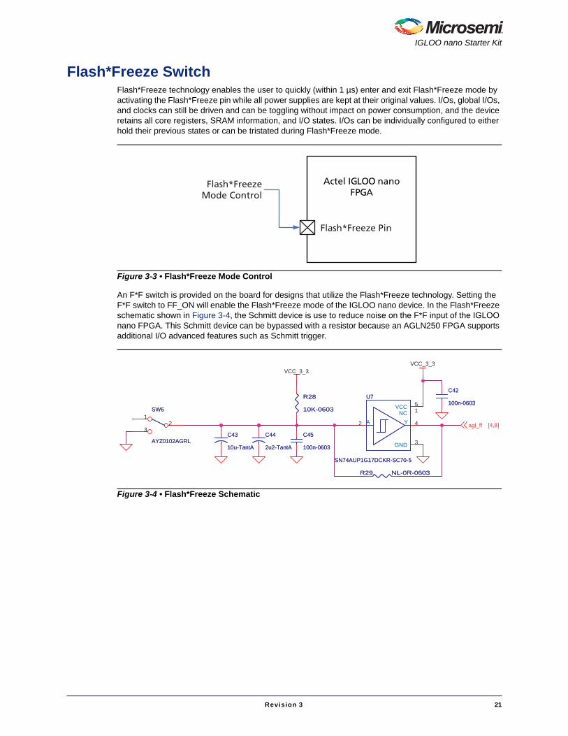
Flash*Freeze SwitchFlash*Freeze technology enables the user to quickly (within 1 µs) enter and exit Flash*Freeze mode by activating the Flash*Freeze pin while all power supplies are kept at their original values. I/Os, global I/Os, and clocks can still be driven and can be toggling without impact on power consumption, and the device retains all core registers, SRAM information, and I/O states. I/Os can be individually configured to either hold their previous states or can be tristated during Flash*Freeze mode.
An F*F switch is provided on the board for designs that utilize the Flash*Freeze technology. Setting the F*F switch to FF_ON will enable the Flash*Freeze mode of the IGLOO nano device. In the Flash*Freeze schematic shown in Figure 3-4, the Schmitt device is use to reduce noise on the F*F input of the IGLOO nano FPGA. This Schmitt device can be bypassed with a resistor because an AGLN250 FPGA supports additional I/O advanced features such as Schmitt trigger.
Figure 3-3 • Flash*Freeze Mode Control
Figure 3-4 • Flash*Freeze Schematic
Actel IGLOO nanoFPGA
Flash*FreezeMode Control
Flash*Freeze Pin
VCC_3_3VCC_3_3
agl_ff [4,8]
C45
100n-0603
C45
100n-0603
21
3
SW6
AYZ0102AGRL
SW6
AYZ0102AGRLC44
2u2-TantA
C44
2u2-TantA
R29 NL-0R-0603R29 NL-0R-0603
C43
10u-TantA
C43
10u-TantA
C42
100n-0603
C42
100n-0603R28
10K-0603
R28
10K-0603NC 1
2 A
GND 3
VCC 5
4Y
U7
SN74AUP1G17DCKR-SC70-5
U7
SN74AUP1G17DCKR-SC70-5
Revision 3 21
Operation of Board Components
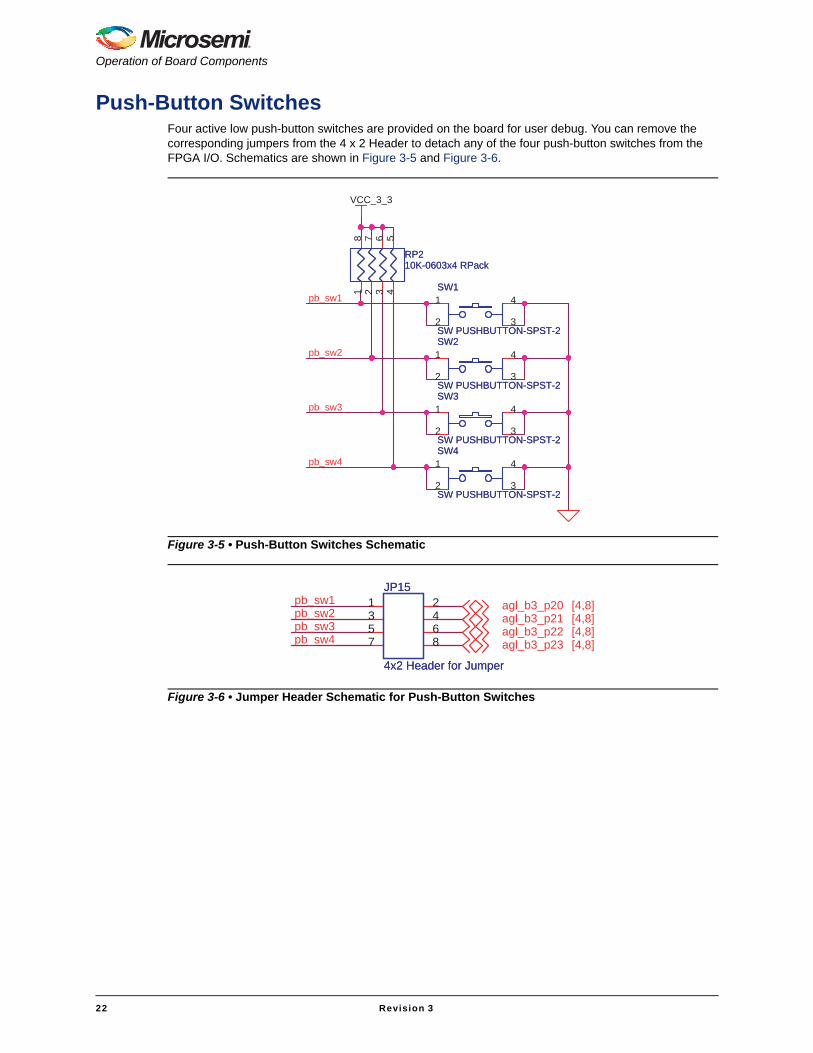
Push-Button SwitchesFour active low push-button switches are provided on the board for user debug. You can remove the corresponding jumpers from the 4 x 2 Header to detach any of the four push-button switches from the FPGA I/O. Schematics are shown in Figure 3-5 and Figure 3-6.
Figure 3-5 • Push-Button Switches Schematic
Figure 3-6 • Jumper Header Schematic for Push-Button Switches
pb_sw1
pb_sw2
pb_sw3
pb_sw4
VCC_3_3
1 4
2 3
SW2
SW PUSHBUTTON-SPST-2
SW2
SW PUSHBUTTON-SPST-2
1 4
2 3
SW3
SW PUSHBUTTON-SPST-2
SW3
SW PUSHBUTTON-SPST-2
1 4
2 3
SW4
SW PUSHBUTTON-SPST-2
SW4
SW PUSHBUTTON-SPST-2
1 2 3 45678
RP210K-0603x4 RPackRP210K-0603x4 RPack
1 4
2 3
SW1
SW PUSHBUTTON-SPST-2
SW1
SW PUSHBUTTON-SPST-2
pb_sw1
pb_sw3pb_sw4
pb_sw2
agl_b3_p23 [4,8]agl_b3_p22 [4,8]agl_b3_p21 [4,8]agl_b3_p20 [4,8]1 2
3 45 67 8
JP15
4x2 Header for Jumper
JP15
4x2 Header for Jumper
22 Revision 3

IGLOO nano Starter Kit
DIP SwitchesA DIP switch pack (8 switches) is provided on the board. You can remove the corresponding jumpers from the 8 x 2 header to detach any of the eight DIP Switches from the FPGA I/O.
Figure 3-7 • DIP Switches Schematic
Figure 3-8 • Jumper Header Schematic for DIP Switches
dip_sw1dip_sw2dip_sw3dip_sw4dip_sw5dip_sw6dip_sw7dip_sw8
VCC_3_3
12345678
161514131211109
SW5
SMD SW DIP-8
SW5
SMD SW DIP-81 2 3 4 5 6 7 8
910111213141516
RP110K-0603x8 RPackRP110K-0603x8 RPack
dip_sw1dip_sw2
dip_sw4dip_sw3
dip_sw7dip_sw6dip_sw5
dip_sw8
agl_b2_p26 [4,8]agl_b2_p28 [4,8]agl_b2_p29 [4,8]agl_b2_p30 [4,8]agl_b2_p31 [4,8]agl_b2_p32 [4,8]agl_b2_p33 [4,8]agl_b2_p34 [4,8]
1 23 45 67 89 10
11 1213 1415 16
JP14
8x2 Header for Jumper
JP14
8x2 Header for Jumper
Revision 3 23

Operation of Board Components
User LEDsEight active low debug LEDs are provided on the board. You can remove the corresponding jumpers from the 8 x 2 headers to detach any of the eight LEDs from the FPGA I/O.
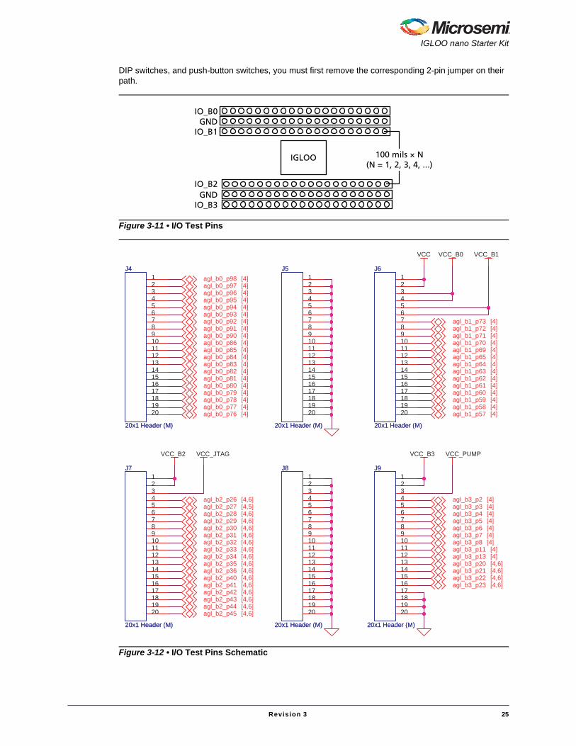
I/O Test PinsAll IGLOO nano FPGA I/Os are available on headers located on the top and bottom of the device. These headers are multiples of 100 mils apart, so you can easily place an extension card on top with an off-the-shelf bread board for a low-cost integration solution. Before you can use the I/Os assigned to the LEDs,
Figure 3-9 • User LEDs Schematic
Figure 3-10 • Jumper Header Schematic for User LEDs
led1
led2
led3
led4
led5
led6
led7
led8
VCC_3_3
1 2LED2 RED SMD LED - 1206LED2 RED SMD LED - 1206
R31 470R-0603R31 470R-0603
1 2LED5 GREEN SMD LED - 1206LED5 GREEN SMD LED - 1206
1 2LED1 RED SMD LED - 1206LED1 RED SMD LED - 1206
R34 470R-0603R34 470R-0603
1 2LED6 GREEN SMD LED - 1206LED6 GREEN SMD LED - 1206
1 2LED3 RED SMD LED - 1206LED3 RED SMD LED - 1206
R35 470R-0603R35 470R-0603
R32 470R-0603R32 470R-0603
1 2LED7 GREEN SMD LED - 1206LED7 GREEN SMD LED - 1206
1 2LED4 RED SMD LED - 1206LED4 RED SMD LED - 1206
R36 470R-0603R36 470R-0603
R33 470R-0603R33 470R-0603
1 2LED8 GREEN SMD LED - 1206LED8 GREEN SMD LED - 1206
R37 470R-0603R37 470R-0603
R30 470R-0603R30 470R-0603
led1led2
led4led3
led7led6led5
led8
agl_b2_p35 [4,8]agl_b2_p36 [4,8]agl_b2_p40 [4,8]agl_b2_p41 [4,8]agl_b2_p42 [4,8]agl_b2_p43 [4,8]agl_b2_p44 [4,8]agl_b2_p45 [4,8]
1 23 45 67 89 10
11 1213 1415 16
JP13
8x2 Header for Jumper
JP13
8x2 Header for Jumper
24 Revision 3
IGLOO nano Starter Kit
DIP switches, and push-button switches, you must first remove the corresponding 2-pin jumper on their path.
Figure 3-11 • I/O Test Pins
Figure 3-12 • I/O Test Pins Schematic
GND
GND
IGLOO
IO_B0
IO_B1
IO_B2
IO_B3
100 mils × N(N = 1, 2, 3, 4, ...)
VCC
VCC_B2 VCC_B3
VCC_B0 VCC_B1
VCC_PUMPVCC_JTAG
agl_b1_p58 [4]agl_b1_p59 [4]agl_b1_p60 [4]agl_b1_p61 [4]agl_b1_p62 [4]agl_b1_p63 [4]agl_b1_p64 [4]agl_b1_p65 [4]agl_b1_p69 [4]agl_b1_p70 [4]agl_b1_p71 [4]agl_b1_p72 [4]agl_b1_p73 [4]
agl_b1_p57 [4]
agl_b2_p34 [4,6]agl_b2_p35 [4,6]agl_b2_p36 [4,6]agl_b2_p40 [4,6]agl_b2_p41 [4,6]agl_b2_p42 [4,6]agl_b2_p43 [4,6]agl_b2_p44 [4,6]agl_b2_p45 [4,6]
agl_b2_p29 [4,6]agl_b2_p30 [4,6]agl_b2_p31 [4,6]agl_b2_p32 [4,6]agl_b2_p33 [4,6]
agl_b2_p26 [4,6]agl_b2_p27 [4,5]agl_b2_p28 [4,6]
agl_b3_p2 [4]agl_b3_p3 [4]agl_b3_p4 [4]agl_b3_p5 [4]agl_b3_p6 [4]agl_b3_p7 [4]agl_b3_p8 [4]agl_b3_p11 [4]agl_b3_p13 [4]agl_b3_p20 [4,6]agl_b3_p21 [4,6]agl_b3_p22 [4,6]agl_b3_p23 [4,6]
agl_b0_p95 [4]agl_b0_p96 [4]
agl_b0_p93 [4]
agl_b0_p91 [4]agl_b0_p92 [4]
agl_b0_p94 [4]
agl_b0_p86 [4]agl_b0_p90 [4]
agl_b0_p84 [4]agl_b0_p83 [4]agl_b0_p82 [4]
agl_b0_p80 [4]agl_b0_p79 [4]agl_b0_p78 [4]
agl_b0_p81 [4]
agl_b0_p76 [4]agl_b0_p77 [4]
agl_b0_p85 [4]
agl_b0_p97 [4]agl_b0_p98 [4]1
234567891011121314151617181920
J4
20x1 Header (M)
J4
20x1 Header (M)
1234567891011121314151617181920
J6
20x1 Header (M)
J6
20x1 Header (M)
1234567891011121314151617181920
J7
20x1 Header (M)
J7
20x1 Header (M)
1234567891011121314151617181920
J9
20x1 Header (M)
J9
20x1 Header (M)
1234567891011121314151617181920
J5
20x1 Header (M)
J5
20x1 Header (M)
1234567891011121314151617181920
J8
20x1 Header (M)
J8
20x1 Header (M)
Revision 3 25
Operation of Board Components
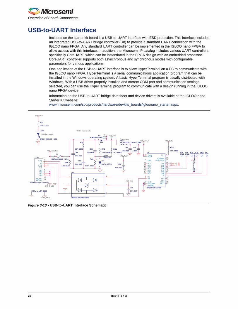
USB-to-UART InterfaceIncluded on the starter kit board is a USB-to-UART interface with ESD protection. This interface includes an integrated USB-to-UART bridge controller (U8) to provide a standard UART connection with the IGLOO nano FPGA. Any standard UART controller can be implemented in the IGLOO nano FPGA to allow access with this interface. In addition, the Microsemi IP catalog includes various UART controllers, specifically CoreUART, which can be instantiated in the FPGA design with an embedded processor. CoreUART controller supports both asynchronous and synchronous modes with configurable parameters for various applications.One application of the USB-to-UART interface is to allow HyperTerminal on a PC to communicate with the IGLOO nano FPGA. HyperTerminal is a serial communications application program that can be installed in the Windows operating system. A basic HyperTerminal program is usually distributed with Windows. With a USB driver properly installed and correct COM port and communication settings selected, you can use the HyperTerminal program to communicate with a design running in the IGLOO nano FPGA device. Information on the USB-to-UART bridge datasheet and device drivers is available at the IGLOO nano Starter Kit website: www.microsemi.com/soc/products/hardware/devkits_boards/igloonano_starter.aspx.
Figure 3-13 • USB-to-UART Interface Schematic
VCC_vbus_f
VCC_vbus
VCC_3_3_1
VCC_usb_vbus
GND_SHLD1
VCC_3_3_1
VCC_vbus
GND_SHLD1
VCC_vbus
agl_txd [4]agl_rxd [4]
USB Connected
USB in-rush Limiter
Ferrite Bead
R48
10K-0603
R48
10K-0603
SP14DCDSP14DCD
R41
2K7-0603
R41
2K7-0603
R38
560R-0603
R38
560R-0603
SP10DTRSP10DTR
1
2
3 4
5
6
U9
USBLC6-2SC6-SOT23-6L
U9
USBLC6-2SC6-SOT23-6L
R42
10K-0603
R42
10K-0603
R4
9N
L-0
R-0
60
3R
49
NL
-0R
-06
03SP11
DSRSP11DSR
SP15RISP15RI
R43
220K-0603
R43
220K-0603
R40
22R-0603
R40
22R-0603
C46
100n-0603
C46
100n-0603
C52
100n-0603
C52
100n-0603
C5027n-0603C5027n-0603
SP12RTSSP12RTS
14256
3
Q4SI3407DV-TSOP6
Q4SI3407DV-TSOP6
V_Bus 1D- 2D+ 3
ID_NC 4GND 5
SH1 6SH2 7SH3 8SH4 9
GP_NC1 10GP_NC2 11
CON2
USB Mini B-Type Connector
CON2
USB Mini B-Type Connector
SP13CTSSP13CTS
C47
1u-0603
C47
1u-0603
VBUS8REGIN7
VDD6
DM5DP4
DTR 28
RTS 24CTS 23
DSR 27
RI 2DCD 1
TXD 26RXD 25
SUSPEND 12SUSPEND_n 11
RST 9
NC110NC213NC314NC415NC516NC617NC718
NC8 19NC9 20
NC10 21NC11 22GND3
GNDNW30 GNDCNTR29
U8
CP2102-GM-MLP28
U8
CP2102-GM-MLP28C53
100n-0603
C53
100n-0603
13
2D2
BAT54-SOT23
D2
BAT54-SOT23
C51
100n-0603
C51
100n-0603
R39
22R-0603
R39
22R-0603
C49
100n-0603
C49
100n-0603
FB2EBMS321611B190-1206FB2EBMS321611B190-1206
12
LED9
GREEN SMD LED - 1206
LED9
GREEN SMD LED - 1206
R44 0R-0603R44 0R-0603
C48
100n-0603
C48
100n-0603
12F1
MICROSMD050F-2-1210
F1
MICROSMD050F-2-1210
26 Revision 3

IGLOO nano Starter Kit
Low-Cost Programming Stick (LCPS)
InterfaceThe development board can be programmed by the low-cost programming stick or via a 10-pin FP3 header (Figure 3-14 on page 27). Regardless of the programming dongle used, IGLOO nano is programmed the same way as IGLOO PLUS, ProASIC3, and Fusion FPGA devices.The LCPS is a special version for the FlashPro3 programming circuitry that is compatible with FlashPro3 and the generic FlashPro programming software. The LCPS, like the IGLOO nano board, is RoHS-compliant and is completely lead (Pb) free. To use the LCPS with the FlashPro software, select FlashPro3 from the list of programmer types. The LCPS behaves exactly as if it were a regular encased FlashPro3 programmer. The LCPS shipped with this Starter Kit is designed for use with the IGLOO nano board and is not supplied as a separately orderable item from Microsemi SoC Products Group. The 12-pin female connector socket is designed to interface with the 12-pin right-angle male header on the IGLOO nano kit. One of the pins is a special VJTAGENB signal that goes high when programming is taking place and returns to a low level when programming has completed. The IGLOO nano board uses this signal to effect a change in the value of VCC from 1.2 V to 1.5 V, which is required for programming all IGLOO nano devices.You do not need to have the LCPS connected to the IGLOO nano board to operate it once the FPGA has been programmed. The IGLOO nano board only needs the LCPS connected when programming the IGLOO AGLN250V2-VQG100.Note: The LCPS supplied with this kit is intended for use with the IGLOO nano Starter Kit. An LCPS
supplied for another kit, although electrically and functionally equivalent, may not connect seamlessly with the IGLOO nano Starter Kit board.
Figure 3-14 • FPGA Programming Headers Schematic
fp3_agl_tck
fp3_agl_tdo
fp3_agl_tms
fp3_agl_trstfp3_agl_tdi
fp3_agl_tms
fp3_agl_tdifp3_agl_trst
fp3_agl_tckfp3_agl_tdo
VCC_JTAG VCC_PUMP
VCC_PUMP VCC_JTAG
agl_tms[4]
agl_tdo[4]
agl_tck [4]
agl_tdi [4]agl_trst [2,4]
agl_tdi[4]
agl_tck[4]
agl_tdo[4]
agl_tms[4]
agl_trst[2,4]
vjtagenb[2]
LCPS Header
1 23 45 67 89 10
11 12
J2
6x2 RA SMD Header (M)
J2
6x2 RA SMD Header (M)
1 23 45 67 89 10
J3
NL-5x2 Header (M)
J3
NL-5x2 Header (M)
R25 NL-0R-0603R25 NL-0R-0603
R23 NL-0R-0603R23 NL-0R-0603
R27 NL-0R-0603R27 NL-0R-0603
R26 NL-0R-0603R26 NL-0R-0603
R24 NL-0R-0603R24 NL-0R-0603
Revision 3 27


4 – Programming
To program a design into the IGLOO nano evaluation board:1. Attach the LCPS board to the IGLOO nano evaluation board.2. Attach a USB cable to the LCPS. This allows a programming data file, in programming database
format (*.pdb) or STAPL format (*.stp), to be downloaded via the FlashPro software to the IGLOO nano device fitted to the board.
3. A separate USB connection is required for the IGLOO nano Board if no other power source is attached to the IGLOO nano Board.
4. When using the FlashPro software, select the FlashPro3 programmer. The LCPS is functionally equivalent to a FlashPro programmer but designed specifically for use with the IGLOO nano kit.
Revision 3 29

5 – Board Demonstration
The IGLOO nano FPGA is pre-programmed with a simple demo to quickly get you started. This demo design will help give a quick overview as well as a quick check of this board. You can easily use this demo as a guide to create your own design for evaluation.The demo design RTL code and design files are available at the IGLOO nano Starter Kit website:
www.microsemi.com/soc/products/hardware/devkits_boards/igloonano_starter.aspx
Powering Up the Board and Running the Demo1. Check and put the board in its default setting.2. Plug the USB cable into a powered USB hub or a powered PC.3. Plug the USB cable into the board to power it up.
The board is powered from the USB connection and no external supply is required. A 5 V wall-jack connector is only provided on the board as an alternative if USB power is not available.
4. On power-up there should not be any activity on the LED (reset condition).5. Refer to the table below for LEDs, push-button switch, and DIP switch functions:
Table 5-1 • Demo Settings
LED Push Button Switch Dip Switch
All 8 LEDs blinking SW4 (User PB 1) Don’t Care
Right Shift (LED1 to LED8) SW5 (User PB 2) Don’t Care
Left Shift (LED8 to LED1) SW6 (User PB 3) Don’t Care
Toggles on respective DIP switch action (for example, LED1 toggles on DIP switch SW3.1 status)
SW7 (User PB 4) DIP Switches are connected to respective LEDs
All 8 LEDs will be off SW1 (Reset PB) Don’t Care
Revision 3 31

A – Resources
IGLOO nano Starter Kitwww.microsemi.com/soc/products/hardware/devkits_boards/igloonano_starter.aspx
IGLOO nano Overviewwww.microsemi.com/soc/products/igloonano/default.aspx
IGLOO nano Datasheetwww.microsemi.com/soc/documents/IGLOO_nano_DS.pdf
IGLOO nano FPGA Fabric User’s Guidewww.microsemi.com/soc/documents/IGLOO_nano_UG.pdf
Microsemi FPGA and SoC Development Softwarewww.microsemi.com/soc/products/software/libero/default.aspx
Revision 3 33


B – List Of Changes
The following table lists critical changes that were made in each revision of the chapter.
Date Changes Page
Revision 3(January 2013)
The document format and website references were changed from Actel to Microsemi; Actel is now Microsemi SoC Products Group. The "Product Support" information was updated.
All
Libero Integrated Design Environment (IDE) was updated to Libero System-on-Chip (SoC) software.
Multi
The jumpers in a small packet and Libero IDE DVD were removed from Table 1 • IGLOO nano Starter Kit Contents.
4
The "Regulatory and Compliance Information" section is new (SAR 43920). 37– 38
Revision 2(September 2010)
The AGLN250-ZVQG100 part was replaced with AGLN250V2-VQG100 throughout the document. References to nano-Z parts were removed (SAR 27593).
3, 11, others
The "FPGA Description: AGLN250V2-VQG100" section was revised to change "PLLs" to "integrated PLLs." The FlashROM bits value in Table 1-2 • Features of AGLN250V2-VQG100 was changed from 1,000 to 1,024 (SAR 27593).
11
The following figures were replaced (SAR 27593):Figure 1-4 • AGLN250V2-VQG100 Banks 0–3 SchematicFigure 1-5 • AGLN250V2-VQG100 JTAG PinsFigure 1-6 • AGLN250V2-VQG100 Power and GND pins
12, 13
The "Reset" section was revised to remove text applicable to nano-Z devices and state that the Schmitt trigger device can be bypassed because an AGLN250 FPGA supports additional I/O advanced features such as Schmitt trigger. A similar revision was made to the "Flash*Freeze Switch" section (SAR 27593).
20, 21
The "LCPS Stackup" section was deleted. N/A
Revision 3 35


C – Product Support
Microsemi SoC Products Group backs its products with various support services, including CustomerService, Customer Technical Support Center, a website, electronic mail, and worldwide sales offices.This appendix contains information about contacting Microsemi SoC Products Group and using thesesupport services.
Customer ServiceContact Customer Service for non-technical product support, such as product pricing, product upgrades,update information, order status, and authorization.
From North America, call 800.262.1060From the rest of the world, call 650.318.4460Fax, from anywhere in the world, 408.643.6913
Customer Technical Support CenterMicrosemi SoC Products Group staffs its Customer Technical Support Center with highly skilledengineers who can help answer your hardware, software, and design questions about Microsemi SoCProducts. The Customer Technical Support Center spends a great deal of time creating applicationnotes, answers to common design cycle questions, documentation of known issues, and various FAQs.So, before you contact us, please visit our online resources. It is very likely we have already answeredyour questions.
Technical SupportVisit the Customer Support website (www.microsemi.com/soc/support/search/default.aspx) for more information and support. Many answers available on the searchable web resource include diagrams, illustrations, and links to other resources on the website.
WebsiteYou can browse a variety of technical and non-technical information on the SoC home page, at www.microsemi.com/soc.
Contacting the Customer Technical Support CenterHighly skilled engineers staff the Technical Support Center. The Technical Support Center can becontacted by email or through the Microsemi SoC Products Group website.
EmailYou can communicate your technical questions to our email address and receive answers back by email,fax, or phone. Also, if you have design problems, you can email your design files to receive assistance.We constantly monitor the email account throughout the day. When sending your request to us, pleasebe sure to include your full name, company name, and your contact information for efficient processing ofyour request.The technical support email address is [email protected].
Revision 3 37

Product Support
My CasesMicrosemi SoC Products Group customers may submit and track technical cases online by going to My Cases.
Outside the U.S.Customers needing assistance outside the US time zones can either contact technical support via email([email protected]) or contact a local sales office. Sales office listings can be found atwww.microsemi.com/soc/company/contact/default.aspx.
ITAR Technical SupportFor technical support on RH and RT FPGAs that are regulated by International Traffic in Arms Regulations (ITAR), contact us via [email protected]. Alternatively, within My Cases, select Yes in the ITAR drop-down list. For a complete list of ITAR-regulated Microsemi FPGAs, visit the ITAR web page.
Regulatory and Compliance Information
EU Declaration of Conformity This product complies to Directive 2011/65/EU of the European Parliament and of the Council of 8 June 2011 on the restriction of the use of certain hazardous substances in electrical and electronic equipment.To view the Declaration of Conformity (English):
http://www.microsemi.com/soc/documents/IGLOO_NANO_DoC.pdf
Markings
This product complies with 2004/108/EC, Electromagnetic Compatibility (EMC) Directive.
38 Revision 3

Index
AAGLN250V2-VQG100 4, 11
features 11I/O banks and pins 12I/O features 13
Bboard
bottom silkscreen 9description 3measurements 4picture 7stackup 8top silkscreen 8
Cclock oscillator specifications 19contacting Microsemi SoC Products Group
customer service 37email 37web-based technical support 37
current measurement 17customer service 37
Ddecoupling capacitors 13demo 31
design files 31instructions 31settings 31
DIP switches 23
FFlash*Freeze mode
control 21switch 21
Hhardware
components 7HyperTerminal 4
II/O test pins 24IGLOO nano Evaluation Board 7
Jjumpers
settings 10
LLCPS 4, 27
interface 27programming 29
LEDs 24low-cost programming stick (LCPS) 4, 27
MMicrosemi SoC Products Group
email 37web-based technical support 37website 37
Pproduct support
customer service 37email 37My Cases 38outside the U.S. 38technical support 37website 37
programming 29push-button reset 20push-button switches 22
Rresources 33, 35
Sschematic
AGLN250V2-VQG100 Banks 0-3 12battery header 16clock oscillator 19current measurement header 18DIP switches 23FPGA programming headers 27I/O test pins 25power input 16power LED regulator 15push-button switches 22reset 20test LEDs 24USB-to-UART 26
schematicFflash*Freeze 21switches
DIP 23push-button 22settings 10
Revision 3 39
Index
Ttech support
ITAR 38My Cases 38outside the U.S. 38
technical support 37
UUSB-to-UART
interface 4User LEDs 24
Wweb-based technical support 37
40 Revision 3


50200146-3/1.13
© 2013 Microsemi Corporation. All rights reserved. Microsemi and the Microsemi logo are trademarks ofMicrosemi Corporation. All other trademarks and service marks are the property of their respective owners.
Microsemi Corporation (NASDAQ: MSCC) offers a comprehensive portfolio of semiconductorsolutions for: aerospace, defense and security; enterprise and communications; and industrialand alternative energy markets. Products include high-performance, high-reliability analogand RF devices, mixed signal and RF integrated circuits, customizable SoCs, FPGAs, andcomplete subsystems. Microsemi is headquartered in Aliso Viejo, Calif. Learn more atwww.microsemi.com.
Microsemi Corporate HeadquartersOne Enterprise, Aliso Viejo CA 92656 USAWithin the USA: +1 (949) 380-6100Sales: +1 (949) 380-6136Fax: +1 (949) 215-4996