
IGLOO nano Low-Power Flash FPGAs Datasheet · IGLOO nano Low-Power Flash FPGAs Advance v0.8 III ......
132
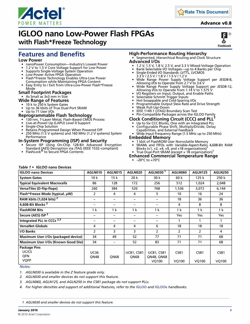
January 2010 I © 2010 Actel Corporation IGLOO nano Low-Power Flash FPGAs with Flash*Freeze Technology Features and Benefits Low Power • nanoPower Consumption—Industry’s Lowest Power • 1.2 V to 1.5 V Core Voltage Support for Low Power • Supports Single-Voltage System Operation • Low-Power Active FPGA Operation • Flash*Freeze Technology Enables Ultra-Low Power Consumption while Maintaining FPGA Content • Easy Entry to / Exit from Ultra-Low-Power Flash*Freeze Mode Small Footprint Packages • As Small as 3x3 mm in Size Wide Range of Features • 10 k to 250 k System Gates • Up to 36 kbits of True Dual-Port SRAM • Up to 71 User I/Os Reprogrammable Flash Technology • 130-nm, 7-Layer Metal, Flash-Based CMOS Process • Live-at-Power-Up (LAPU) Level 0 Support • Single-Chip Solution • Retains Programmed Design When Powered Off • 250 MHz (1.5 V systems) and 160 MHz (1.2 V systems) System Performance In-System Programming (ISP) and Security • Secure ISP Using On-Chip 128-Bit Advanced Encryption Standard (AES) Decryption via JTAG (IEEE 1532–compliant) • FlashLock ® to Secure FPGA Contents High-Performance Routing Hierarchy • Segmented, Hierarchical Routing and Clock Structure Advanced I/Os • 1.2 V, 1.5 V, 1.8 V, 2.5 V, and 3.3 V Mixed-Voltage Operation • Bank-Selectable I/O Voltages—up to 4 Banks per Chip • Single-Ended I/O Standards: LVTTL, LVCMOS 3.3 V / 2.5 V / 1.8 V / 1.5 V / 1.2 V • Wide Range Power Supply Voltage Support per JESD8-B, Allowing I/Os to Operate from 2.7 V to 3.6 V • Wide Range Power Supply Voltage Support per JESD8-12, Allowing I/Os to Operate from 1.14 V to 1.575 V • I/O Registers on Input, Output, and Enable Paths • Selectable Schmitt Trigger Inputs • Hot-Swappable and Cold-Sparing I/Os • Programmable Output Slew Rate and Drive Strength • Weak Pull-Up/-Down • IEEE 1149.1 (JTAG) Boundary Scan Test • Pin-Compatible Packages across the IGLOO Family Clock Conditioning Circuit (CCC) and PLL † • Up to Six CCC Blocks, One with an Integrated PLL • Configurable Phase Shift, Multiply/Divide, Delay Capabilities, and External Feedback • Wide Input Frequency Range (1.5 MHz up to 250 MHz) Embedded Memory • 1 kbit of FlashROM User Nonvolatile Memory • SRAMs and FIFOs with Variable-Aspect-Ratio 4,608-Bit RAM Blocks (×1, ×2, ×4, ×9, and ×18 organizations) † • True Dual-Port SRAM (except × 18 organization) † Enhanced Commercial Temperature Range • –20°C to +70°C ® † AGLN030 and smaller devices do not support this feature. Table 1 • IGLOO nano Devices IGLOO nano Devices AGLN010 AGLN015 AGLN020 AGLN030 1 AGLN060 AGLN125 AGLN250 System Gates 10 k 15 k 20 k 30 k 60 k 125 k 250 k Typical Equivalent Macrocells 86 128 172 256 512 1,024 2,048 VersaTiles (D-flip-flops) 260 384 520 768 1,536 3,072 6,144 Flash*Freeze Mode (typical, μW) 2 4 4 5 10 16 24 RAM kbits (1,024 bits) 2 – – – – 18 36 36 4,608-Bit Blocks 2 – – – – 4 8 8 FlashROM Bits 1 k 1 k 1 k 1 k 1 k 1 k 1 k Secure (AES) ISP 2 – – – – Yes Yes Yes Integrated PLL in CCCs 2,3 – – – – 1 1 1 VersaNet Globals 4 4 4 6 18 18 18 I/O Banks 2 3 3 2 2 2 4 Maximum User I/Os (packaged device) 34 49 52 77 71 71 68 Maximum User I/Os (Known Good Die) 34 – 52 83 71 71 68 Package Pins UC/CS QFN VQFP UC36 QN48 QN68 UC81, CS81 QN68 UC81, CS81 QN48, QN68 VQ100 CS81 VQ100 CS81 VQ100 CS81 VQ100 Notes: 1. AGLN030 is available in the Z feature grade only. 2. AGLN030 and smaller devices do not support this feature. 3. AGLN060, AGLN125, and AGLN250 in the CS81 package do not support PLLs. 4. For higher densities and support of additional features, refer to the IGLOO and IGLOOe handbooks. Advance v0.8
Transcript of IGLOO nano Low-Power Flash FPGAs Datasheet · IGLOO nano Low-Power Flash FPGAs Advance v0.8 III ......
Advance v0.8
IGLOO nano Low-Power Flash FPGAswith Flash*Freeze Technology
Features and BenefitsLow Power
• nanoPower Consumption—Industry’s Lowest Power • 1.2 V to 1.5 V Core Voltage Support for Low Power• Supports Single-Voltage System Operation• Low-Power Active FPGA Operation • Flash*Freeze Technology Enables Ultra-Low Power
Consumption while Maintaining FPGA Content• Easy Entry to / Exit from Ultra-Low-Power Flash*Freeze
ModeSmall Footprint Packages
• As Small as 3x3 mm in SizeWide Range of Features
• 10 k to 250 k System Gates• Up to 36 kbits of True Dual-Port SRAM• Up to 71 User I/Os
Reprogrammable Flash Technology• 130-nm, 7-Layer Metal, Flash-Based CMOS Process• Live-at-Power-Up (LAPU) Level 0 Support• Single-Chip Solution• Retains Programmed Design When Powered Off• 250 MHz (1.5 V systems) and 160 MHz (1.2 V systems) System
PerformanceIn-System Programming (ISP) and Security
• Secure ISP Using On-Chip 128-Bit Advanced EncryptionStandard (AES) Decryption via JTAG (IEEE 1532–compliant)
• FlashLock® to Secure FPGA Contents
High-Performance Routing Hierarchy• Segmented, Hierarchical Routing and Clock Structure
Advanced I/Os• 1.2 V, 1.5 V, 1.8 V, 2.5 V, and 3.3 V Mixed-Voltage Operation• Bank-Selectable I/O Voltages—up to 4 Banks per Chip• Single-Ended I/O Standards: LVTTL, LVCMOS
3.3 V / 2.5 V / 1.8 V / 1.5 V / 1.2 V• Wide Range Power Supply Voltage Support per JESD8-B,
Allowing I/Os to Operate from 2.7 V to 3.6 V• Wide Range Power Supply Voltage Support per JESD8-12,
Allowing I/Os to Operate from 1.14 V to 1.575 V• I/O Registers on Input, Output, and Enable Paths• Selectable Schmitt Trigger Inputs• Hot-Swappable and Cold-Sparing I/Os• Programmable Output Slew Rate and Drive Strength• Weak Pull-Up/-Down• IEEE 1149.1 (JTAG) Boundary Scan Test• Pin-Compatible Packages across the IGLOO Family
Clock Conditioning Circuit (CCC) and PLL†
• Up to Six CCC Blocks, One with an Integrated PLL• Configurable Phase Shift, Multiply/Divide, Delay
Capabilities, and External Feedback• Wide Input Frequency Range (1.5 MHz up to 250 MHz)
Embedded Memory• 1 kbit of FlashROM User Nonvolatile Memory• SRAMs and FIFOs with Variable-Aspect-Ratio 4,608-Bit RAM
Blocks (×1, ×2, ×4, ×9, and ×18 organizations)†• True Dual-Port SRAM (except × 18 organization)†
Enhanced Commercial Temperature Range• –20°C to +70°C
®
† AGLN030 and smaller devices do not support this feature.
Table 1 • IGLOO nano DevicesIGLOO nano Devices AGLN010 AGLN015 AGLN020 AGLN030 1 AGLN060 AGLN125 AGLN250
System Gates 10 k 15 k 20 k 30 k 60 k 125 k 250 k
Typical Equivalent Macrocells 86 128 172 256 512 1,024 2,048
VersaTiles (D-flip-flops) 260 384 520 768 1,536 3,072 6,144
Flash*Freeze Mode (typical, µW) 2 4 4 5 10 16 24
RAM kbits (1,024 bits) 2 – – – – 18 36 36
4,608-Bit Blocks 2 – – – – 4 8 8
FlashROM Bits 1 k 1 k 1 k 1 k 1 k 1 k 1 k
Secure (AES) ISP 2 – – – – Yes Yes Yes
Integrated PLL in CCCs 2,3 – – – – 1 1 1
VersaNet Globals 4 4 4 6 18 18 18
I/O Banks 2 3 3 2 2 2 4
Maximum User I/Os (packaged device) 34 49 52 77 71 71 68
Maximum User I/Os (Known Good Die) 34 – 52 83 71 71 68
Package PinsUC/CSQFNVQFP
UC36QN48 QN68
UC81, CS81QN68
UC81, CS81QN48, QN68
VQ100
CS81
VQ100
CS81
VQ100
CS81
VQ100
Notes:
1. AGLN030 is available in the Z feature grade only.2. AGLN030 and smaller devices do not support this feature.3. AGLN060, AGLN125, and AGLN250 in the CS81 package do not support PLLs.
4. For higher densities and support of additional features, refer to the IGLOO and IGLOOe handbooks.
January 2010 I© 2010 Actel Corporation
IGLOO nano Low-Power Flash FPGAs
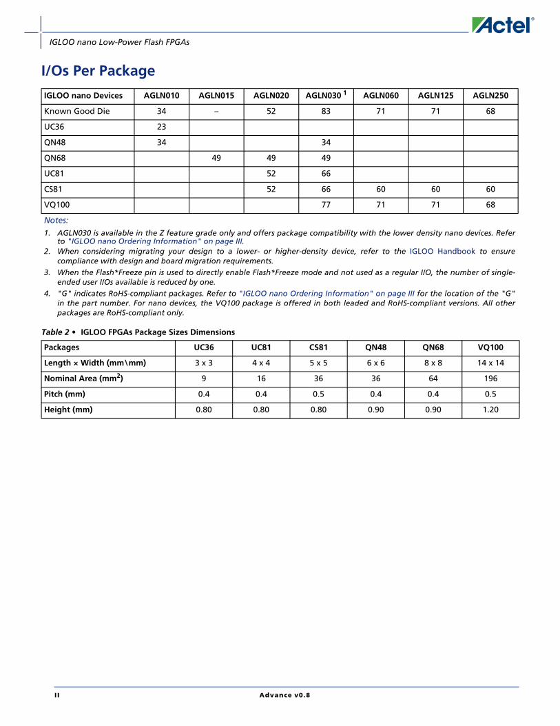
I/Os Per Package
IGLOO nano Devices AGLN010 AGLN015 AGLN020 AGLN030 1 AGLN060 AGLN125 AGLN250
Known Good Die 34 – 52 83 71 71 68
UC36 23
QN48 34 34
QN68 49 49 49
UC81 52 66
CS81 52 66 60 60 60
VQ100 77 71 71 68
Notes:
1. AGLN030 is available in the Z feature grade only and offers package compatibility with the lower density nano devices. Referto "IGLOO nano Ordering Information" on page III.
2. When considering migrating your design to a lower- or higher-density device, refer to the IGLOO Handbook to ensurecompliance with design and board migration requirements.
3. When the Flash*Freeze pin is used to directly enable Flash*Freeze mode and not used as a regular I/O, the number of single-ended user I/Os available is reduced by one.
4. "G" indicates RoHS-compliant packages. Refer to "IGLOO nano Ordering Information" on page III for the location of the "G"in the part number. For nano devices, the VQ100 package is offered in both leaded and RoHS-compliant versions. All otherpackages are RoHS-compliant only.
Table 2 • IGLOO FPGAs Package Sizes Dimensions
Packages UC36 UC81 CS81 QN48 QN68 VQ100
Length × Width (mm\mm) 3 x 3 4 x 4 5 x 5 6 x 6 8 x 8 14 x 14
Nominal Area (mm2) 9 16 36 36 64 196
Pitch (mm) 0.4 0.4 0.5 0.4 0.4 0.5
Height (mm) 0.80 0.80 0.80 0.90 0.90 1.20
I I Advance v0.8

IGLOO nano Low-Power Flash FPGAs
IGLOO nano Ordering Information
Device MarkingActel normally topside marks the full ordering part number on each device. There are some exceptions to this, such as someof the Z feature grade nano devices, the V2 designator for IGLOO devices, and packages where space is physically limited.Packages that have limited characters available are UC36, UC81, CS81, QN48, QN68, and QFN132. On these specific packages,a subset of the device marking will be used that includes the required legal information and as much of the part number asallowed by character limitation of the device. In this case, devices will have a truncated device marking and may exclude theapplications markings, such as the I designator for Industrial Devices or the ES designator for Engineering Samples.
Notes:
1. For the AGLN060, AGLN125, and AGLN250, the Z feature grade does not support the enhanced nano features of Schmitt triggerinput, bus hold, cold-sparing, and hot-swap I/O capability. The AGLN030 Z feature grade does not support Schmitt trigger inputand bus hold. For the VQ100, CS81, UC81, QN68, and QN48 packages, the Z feature grade and the N part number are not markedon the device.
2. Marking Information: IGLOO nano V2 devices do not have V2 marking, but IGLOO nano V5 devices are marked with a V5designator.
AGLN010 = 10,000 System Gates AGLN015 = 15,000 System Gates AGLN020 = 20,000 System Gates AGLN030 = 30,000 System Gates AGLN060 = 60,000 System Gates AGLN125 = 125,000 System Gates AGLN250 = 250,000 System Gates
Blank = StandardZ = nano devices without enhanced features1
Supply Voltage 2 = 1.2 V to 1.5 V5 = 1.5 V only
AGLN250 V2 Z VQ_
Part Number
IGLOO nano Devices
Package Type
VQ = Very Thin Quad Flat Pack (0.5 mm pitch) DIELOT = Known Good Die
QN = Quad Flat Pack No Leads (0.4 mm and 0.5 mm pitches)
100 I
Package Lead Count
G
Lead-Free Packaging
Application (Temperature Range)Blank = Commercial (–20°C to +70°C Ambient Temperature)
I = Industrial (–40°C to +85°C Ambient Temperature)
Blank = Standard PackagingG= RoHS-Compliant Packaging
PP = Pre-ProductionES = Engineering Sample (Room Temperature Only)
CS = Chip Scale Package (0.5 mm pitch)UC = Micro Chip Scale Package (0.4 mm pitch)
Advance v0.8 III

IGLOO nano Low-Power Flash FPGAs
Figure 1 shows an example of device marking based on the AGL030V5-UCG81. The actual mark will vary by thedevice/package combination ordered.
IGLOO nano Product Available in the Z Feature Grade
Temperature Grade Offerings
Contact your local Actel representative for device availability: http://www.actel.com/contact/default.aspx.
Figure 1 • Example of Device Marking for Small Form Factor Packages
Devices AGLN030 AGLN060 AGLN125 AGLN250
Packages QN48 – – –
QN68 – – –
UC81 – – –
CS81 CS81 CS81 CS81
VQ100 VQ100 VQ100 VQ100
Package AGLN010 AGLN015 AGLN020 AGLN030 AGLN060 AGLN125 AGLN250
UC36 C, I – – – – – –
QN48 C, I – – C, I – – –
QN68 – C, I C, I C, I – – –
UC81 – – C, I C, I – – –
CS81 – – C, I C, I C, I C, I C, I
VQ100 – – – C, I C, I C, I C, I
Notes:
1. C = Commercial temperature range: –20°C to 70°C ambient temperature.2. I = Industrial temperature range: –40°C to 85°C ambient temperature.
ACTELXXXAGL030YWWUCG81XXXXXXXXXXXX
Country of Origin
Date Code
Customer Mark(if applicable)
Device Name(six characters)
Package
Wafer Lot #
IV Advance v0.8

1 – IGLOO nano Device Overview
General DescriptionThe IGLOO family of flash FPGAs, based on a 130-nm flash process, offers the lowest power FPGA, asingle-chip solution, small footprint packages, reprogrammability, and an abundance of advancedfeatures.
The Flash*Freeze technology used in IGLOO nano devices enables entering and exiting an ultra-low-power mode that consumes nanoPower while retaining SRAM and register data. Flash*Freezetechnology simplifies power management through I/O and clock management with rapid recoveryto operation mode.
The Low Power Active capability (static idle) allows for ultra-low-power consumption while theIGLOO nano device is completely functional in the system. This allows the IGLOO nano device tocontrol system power management based on external inputs (e.g., scanning for keyboard stimulus)while consuming minimal power.
Nonvolatile flash technology gives IGLOO nano devices the advantage of being a secure, low-power, single-chip solution that is live at power-up (LAPU). The IGLOO nano device isreprogrammable and offers time-to-market benefits at an ASIC-level unit cost.
These features enable designers to create high-density systems using existing ASIC or FPGA designflows and tools.
IGLOO nano devices offer 1 kbit of on-chip, reprogrammable, nonvolatile FlashROM storage as wellas clock conditioning circuitry based on an integrated phase-locked loop (PLL). The AGLN030 andsmaller devices have no PLL or RAM support. IGLOO nano devices have up to 250 k system gates,supported with up to 36 kbits of true dual-port SRAM and up to 71 user I/Os.
IGLOO nano devices increase the breadth of the IGLOO product line by adding new features andpackages for greater customer value in high volume consumer, portable, and battery-backedmarkets. Features such as smaller footprint packages designed with two-layer PCBs in mind, powerconsumption measured in nanoPower, Schmitt trigger, and bus hold functionality make thesedevices ideal for deployment in applications that require high levels of flexibility and low cost.
Flash*Freeze TechnologyThe IGLOO nano device offers unique Flash*Freeze technology, allowing the device to enter andexit ultra-low-power Flash*Freeze mode. IGLOO nano devices do not need additional componentsto turn off I/Os or clocks while retaining the design information, SRAM content, and registers.Flash*Freeze technology is combined with in-system programmability, which enables users toquickly and easily upgrade and update their designs in the final stages of manufacturing or in thefield. The ability of IGLOO nano V2 devices to support a wide range of core voltage (1.2 V to 1.5 V)allows further reduction in power consumption, thus achieving the lowest total system power.
During Flash*Freeze mode, each I/O can be set to the following configurations: hold previous state,tristate, HIGH, or LOW.
The availability of low-power modes, combined with reprogrammability, a single-chip and single-voltage solution, and small-footprint packages make IGLOO nano devices the best fit for portableelectronics.
Advance v0.8 1-1

IGLOO nano Device Overview
Flash Advantages
Low PowerFlash-based IGLOO nano devices exhibit power characteristics similar to those of an ASIC, makingthem an ideal choice for power-sensitive applications. IGLOO nano devices have only a very limitedpower-on current surge and no high-current transition period, both of which occur on manyFPGAs.
IGLOO nano devices also have low dynamic power consumption to further maximize powersavings; power is reduced even further by the use of a 1.2 V core voltage.
Low dynamic power consumption, combined with low static power consumption and Flash*Freezetechnology, gives the IGLOO nano device the lowest total system power offered by any FPGA.
SecurityNonvolatile, flash-based IGLOO nano devices do not require a boot PROM, so there is no vulnerableexternal bitstream that can be easily copied. IGLOO nano devices incorporate FlashLock, whichprovides a unique combination of reprogrammability and design security without externaloverhead, advantages that only an FPGA with nonvolatile flash programming can offer.
IGLOO nano devices utilize a 128-bit flash-based lock and a separate AES key to secureprogrammed intellectual property and configuration data. In addition, all FlashROM data in IGLOOnano devices can be encrypted prior to loading, using the industry-leading AES-128 (FIPS192) bitblock cipher encryption standard. AES was adopted by the National Institute of Standards andTechnology (NIST) in 2000 and replaces the 1977 DES standard. IGLOO nano devices have a built-inAES decryption engine and a flash-based AES key that make them the most comprehensiveprogrammable logic device security solution available today. IGLOO nano devices with AES-basedsecurity allow for secure, remote field updates over public networks such as the Internet, andensure that valuable IP remains out of the hands of system overbuilders, system cloners, and IPthieves. The contents of a programmed IGLOO nano device cannot be read back, although securedesign verification is possible.
Security, built into the FPGA fabric, is an inherent component of IGLOO nano devices. The flash cellsare located beneath seven metal layers, and many device design and layout techniques have beenused to make invasive attacks extremely difficult. IGLOO nano devices, with FlashLock and AESsecurity, are unique in being highly resistant to both invasive and noninvasive attacks. Yourvaluable IP is protected and secure, making remote ISP possible. An IGLOO nano device providesthe most impenetrable security for programmable logic designs.
Single ChipFlash-based FPGAs store their configuration information in on-chip flash cells. Once programmed,the configuration data is an inherent part of the FPGA structure, and no external configurationdata needs to be loaded at system power-up (unlike SRAM-based FPGAs). Therefore, flash-basedIGLOO nano FPGAs do not require system configuration components such as EEPROMs ormicrocontrollers to load device configuration data. This reduces bill-of-materials costs and PCBarea, and increases security and system reliability.
Live at Power-UpActel flash-based IGLOO nano devices support Level 0 of the LAPU classification standard. Thisfeature helps in system component initialization, execution of critical tasks before the processorwakes up, setup and configuration of memory blocks, clock generation, and bus activitymanagement. The LAPU feature of flash-based IGLOO nano devices greatly simplifies total systemdesign and reduces total system cost, often eliminating the need for CPLDs and clock generationPLLs. In addition, glitches and brownouts in system power will not corrupt the IGLOO nano device'sflash configuration, and unlike SRAM-based FPGAs, the device will not have to be reloaded whensystem power is restored. This enables the reduction or complete removal of the configurationPROM, expensive voltage monitor, brownout detection, and clock generator devices from the PCBdesign. Flash-based IGLOO nano devices simplify total system design and reduce cost and designrisk while increasing system reliability and improving system initialization time.
IGLOO nano flash FPGAs enable the user to quickly enter and exit Flash*Freeze mode. This is donealmost instantly (within 1 µs) and the device retains configuration and data in registers and RAM.
1-2 Advance v0.8

IGLOO nano Device Overview
Unlike SRAM-based FPGAs, the device does not need to reload configuration and design state fromexternal memory components; instead it retains all necessary information to resume operationimmediately.
Reduced Cost of OwnershipAdvantages to the designer extend beyond low unit cost, performance, and ease of use. UnlikeSRAM-based FPGAs, flash-based IGLOO nano devices allow all functionality to be live at power-up;no external boot PROM is required. On-board security mechanisms prevent access to all theprogramming information and enable secure remote updates of the FPGA logic. Designers canperform secure remote in-system reprogramming to support future design iterations and fieldupgrades with confidence that valuable intellectual property cannot be compromised or copied.Secure ISP can be performed using the industry-standard AES algorithm. The IGLOO nano devicearchitecture mitigates the need for ASIC migration at higher user volumes. This makes IGLOO nanodevices cost-effective ASIC replacement solutions, especially for applications in the consumer,networking/communications, computing, and avionics markets.
With a variety of devices under $1, Actel IGLOO nano FPGAs enable cost-effective implementationof programmable logic and quick time to market.
Firm-Error ImmunityFirm errors occur most commonly when high-energy neutrons, generated in the upper atmosphere,strike a configuration cell of an SRAM FPGA. The energy of the collision can change the state of theconfiguration cell and thus change the logic, routing, or I/O behavior in an unpredictable way.These errors are impossible to prevent in SRAM FPGAs. The consequence of this type of error can bea complete system failure. Firm errors do not exist in the configuration memory of IGLOO nanoflash-based FPGAs. Once it is programmed, the flash cell configuration element of IGLOO nanoFPGAs cannot be altered by high-energy neutrons and is therefore immune to them. Recoverable(or soft) errors occur in the user data SRAM of all FPGA devices. These can easily be mitigated byusing error detection and correction (EDAC) circuitry built into the FPGA fabric.
Advanced Flash TechnologyThe IGLOO nano device offers many benefits, including nonvolatility and reprogrammability,through an advanced flash-based, 130-nm LVCMOS process with seven layers of metal. StandardCMOS design techniques are used to implement logic and control functions. The combination offine granularity, enhanced flexible routing resources, and abundant flash switches allows for veryhigh logic utilization without compromising device routability or performance. Logic functionswithin the device are interconnected through a four-level routing hierarchy.
IGLOO nano FPGAs utilize design and process techniques to minimize power consumption in allmodes of operation.
Advanced ArchitectureThe proprietary IGLOO nano architecture provides granularity comparable to standard-cell ASICs.The IGLOO nano device consists of five distinct and programmable architectural features(Figure 1-3 on page 1-5 to Figure 1-4 on page 1-5):
• Flash*Freeze technology
• FPGA VersaTiles
• Dedicated FlashROM
• Dedicated SRAM/FIFO memory†
• Extensive CCCs and PLLs†
• Advanced I/O structure
The FPGA core consists of a sea of VersaTiles. Each VersaTile can be configured as a three-inputlogic function, a D-flip-flop (with or without enable), or a latch by programming the appropriateflash switch interconnections. The versatility of the IGLOO nano core tile as either a three-inputlookup table (LUT) equivalent or a D-flip-flop/latch with enable allows for efficient use of the FPGAfabric. The VersaTile capability is unique to the Actel ProASIC® family of third-generation-
† The AGLN030 and smaller devices do not support PLL or SRAM.
Advance v0.8 1-3

IGLOO nano Device Overview
architecture flash FPGAs. VersaTiles are connected with any of the four levels of routing hierarchy.Flash switches are distributed throughout the device to provide nonvolatile, reconfigurableinterconnect programming. Maximum core utilization is possible for virtually any design.
In addition, extensive on-chip programming circuitry enables rapid, single-voltage (3.3 V)programming of IGLOO nano devices via an IEEE 1532 JTAG interface.
Note: *Bank 0 for the AGLN030 deviceFigure 1-1 • IGLOO Device Architecture Overview with Two I/O Banks and No RAM (AGLN010 and AGLN030)
Figure 1-2 • IGLOO Device Architecture Overview with Three I/O Banks and No RAM (AGLN015 and AGLN020)
VersaTile
I/Os
User NonvolatileFlashROM
Flash*FreezeTechnology
ChargePumps
Bank 1*
Ban
k 1
Ban
k 0
Bank 1CCC-GL
CCC-GL
VersaTile
I/Os
User NonvolatileFlashRom
Flash*FreezeTechnology
ChargePumps
Bank 1
Ban
k 2
Ban
k 0
Bank 1
1-4 Advance v0.8

IGLOO nano Device Overview
.
Figure 1-3 • IGLOO Device Architecture Overview with Two I/O Banks (AGLN060, AGLN125)
Figure 1-4 • IGLOO Device Architecture Overview with Four I/O Banks (AGLN250)
RAM Block 4,608-Bit Dual-PortSRAM or FIFO Block
VersaTile
CCC
I/Os
ISP AESDecryption
User NonvolatileFlashRom
Flash*FreezeTechnology
ChargePumps
Bank 0B
ank
1B
ank
1 Ban
k 0B
ank 0
Bank 1
RAM Block 4,608-Bit Dual-PortSRAM or FIFO Block
VersaTile
CCC
I/Os
Bank 0
Ban
k 3
Ban
k 3 B
ank 1
Ban
k 1
Bank 2
ISP AESDecryption
User NonvolatileFlashRom
Flash*FreezeTechnology
ChargePumps
Advance v0.8 1-5

IGLOO nano Device Overview
Flash*Freeze TechnologyThe IGLOO nano device has an ultra-low-power static mode, called Flash*Freeze mode, whichretains all SRAM and register information and can still quickly return to normal operation.Flash*Freeze technology enables the user to quickly (within 1 µs) enter and exit Flash*Freeze modeby activating the Flash*Freeze pin while all power supplies are kept at their original values. I/Os,global I/Os, and clocks can still be driven and can be toggling without impact on powerconsumption, and the device retains all core registers, SRAM information, and I/O states. I/Os canbe individually configured to either hold their previous state or be tristated during Flash*Freezemode.
Alternatively, I/Os can be set to a specific state using weak pull-up or pull-down I/O attributeconfiguration. No power is consumed by the I/O banks, clocks, JTAG pins, or PLL, and the deviceconsumes as little as 2 µW in this mode.
Flash*Freeze technology allows the user to switch to Active mode on demand, thus simplifying thepower management of the device.
The Flash*Freeze pin (active low) can be routed internally to the core to allow the user's logic todecide when it is safe to transition to this mode. Refer to Figure 1-5 for an illustration ofentering/exiting Flash*Freeze mode. It is also possible to use the Flash*Freeze pin as a regular I/O ifFlash*Freeze mode usage is not planned.
VersaTilesThe IGLOO nano core consists of VersaTiles, which have been enhanced beyond the ProASICPLUS®
core tiles. The IGLOO nano VersaTile supports the following:
• All 3-input logic functions—LUT-3 equivalent
• Latch with clear or set
• D-flip-flop with clear or set
• Enable D-flip-flop with clear or set
Refer to Figure 1-6 for VersaTile configurations.
Figure 1-5 • IGLOO nano Flash*Freeze Mode
Actel IGLOO NanoFPGA
Flash*FreezeMode Control
Flash*Freeze Pin
Figure 1-6 • VersaTile Configurations
X1YX2
X3LUT-3
Data Y
CLK
Enable
CLR
D-FFData YCLKCLR
D-FF
LUT-3 Equivalent D-Flip-Flop with Clear or Set Enable D-Flip-Flop with Clear or Set
1-6 Advance v0.8

IGLOO nano Device Overview
User Nonvolatile FlashROM Actel IGLOO nano devices have 1 kbit of on-chip, user-accessible, nonvolatile FlashROM. TheFlashROM can be used in diverse system applications:
• Internet protocol addressing (wireless or fixed)
• System calibration settings
• Device serialization and/or inventory control
• Subscription-based business models (for example, set-top boxes)
• Secure key storage for secure communications algorithms
• Asset management/tracking
• Date stamping
• Version management
The FlashROM is written using the standard IGLOO nano IEEE 1532 JTAG programming interface.The core can be individually programmed (erased and written), and on-chip AES decryption can beused selectively to securely load data over public networks (except in the AGLN030 and smallerdevices), as in security keys stored in the FlashROM for a user design.
The FlashROM can be programmed via the JTAG programming interface, and its contents can beread back either through the JTAG programming interface or via direct FPGA core addressing. Notethat the FlashROM can only be programmed from the JTAG interface and cannot be programmedfrom the internal logic array.
The FlashROM is programmed as 8 banks of 128 bits; however, reading is performed on a byte-by-byte basis using a synchronous interface. A 7-bit address from the FPGA core defines which of the 8banks and which of the 16 bytes within that bank are being read. The three most significant bits(MSBs) of the FlashROM address determine the bank, and the four least significant bits (LSBs) ofthe FlashROM address define the byte.
The Actel IGLOO nano development software solutions, Libero® Integrated Design Environment(IDE) and Designer, have extensive support for the FlashROM. One such feature is auto-generationof sequential programming files for applications requiring a unique serial number in each part.Another feature enables the inclusion of static data for system version control. Data for theFlashROM can be generated quickly and easily using Actel Libero IDE and Designer software tools.Comprehensive programming file support is also included to allow for easy programming of largenumbers of parts with differing FlashROM contents.
SRAM and FIFOIGLOO nano devices (except the AGLN030 and smaller devices) have embedded SRAM blocks alongtheir north and south sides. Each variable-aspect-ratio SRAM block is 4,608 bits in size. Availablememory configurations are 256×18, 512×9, 1k×4, 2k×2, and 4k×1 bits. The individual blocks haveindependent read and write ports that can be configured with different bit widths on each port.For example, data can be sent through a 4-bit port and read as a single bitstream. The embeddedSRAM blocks can be initialized via the device JTAG port (ROM emulation mode) using the UJTAGmacro (except in the AGLN030 and smaller devices).
In addition, every SRAM block has an embedded FIFO control unit. The control unit allows theSRAM block to be configured as a synchronous FIFO without using additional core VersaTiles. TheFIFO width and depth are programmable. The FIFO also features programmable Almost Empty(AEMPTY) and Almost Full (AFULL) flags in addition to the normal Empty and Full flags. Theembedded FIFO control unit contains the counters necessary for generation of the read and writeaddress pointers. The embedded SRAM/FIFO blocks can be cascaded to create larger configurations.
Advance v0.8 1-7

IGLOO nano Device Overview
PLL and CCCHigher density IGLOO nano devices using either the two I/O bank or four I/O bank architecturesprovide designers with very flexible clock conditioning capabilities. AGLN060, AGLN125, andAGLN250 contain six CCCs. One CCC (center west side) has a PLL. The AGLN030 and smaller devicesuse different CCCs in their architecture (CCC-GL). These CCC-GLs contain a global MUX but do nothave any PLLs or programmable delays.
For devices using the six CCC block architecture, these are located at the four corners and thecenters of the east and west sides. All six CCC blocks are usable; the four corner CCCs and the eastCCC allow simple clock delay operations as well as clock spine access.
The inputs of the six CCC blocks are accessible from the FPGA core or from dedicated connectionsto the CCC block, which are located near the CCC.
The CCC block has these key features:
• Wide input frequency range (fIN_CCC) = 1.5 MHz up to 250 MHz
• Output frequency range (fOUT_CCC) = 0.75 MHz up to 250 MHz
• 2 programmable delay types for clock skew minimization
• Clock frequency synthesis (for PLL only)
Additional CCC specifications:
• Internal phase shift = 0°, 90°, 180°, and 270°. Output phase shift depends on the outputdivider configuration (for PLL only).
• Output duty cycle = 50% ± 1.5% or better (for PLL only)
• Low output jitter: worst case < 2.5% × clock period peak-to-peak period jitter when singleglobal network used (for PLL only)
• Maximum acquisition time is 300 µs (for PLL only)
• Exceptional tolerance to input period jitter—allowable input jitter is up to 1.5 ns (for PLLonly)
• Four precise phases; maximum misalignment between adjacent phases of 40 ps × 250 MHz /fOUT_CCC (for PLL only)
Global ClockingIGLOO nano devices have extensive support for multiple clocking domains. In addition to the CCCand PLL support described above, there is a comprehensive global clock distribution network.
Each VersaTile input and output port has access to nine VersaNets: six chip (main) and threequadrant global networks. The VersaNets can be driven by the CCC or directly accessed from thecore via multiplexers (MUXes). The VersaNets can be used to distribute low-skew clock signals or forrapid distribution of high-fanout nets.
I/Os with Advanced I/O StandardsIGLOO nano FPGAs feature a flexible I/O structure, supporting a range of voltages (1.2 V, 1.5 V,1.8 V, 2.5 V, 3.0 V wide range, and 3.3 V).
The I/Os are organized into banks with two, three, or four banks per device. The configuration ofthese banks determines the I/O standards supported.
Each I/O module contains several input, output, and enable registers. These registers allow theimplementation of various single-data-rate applications for all versions of nano devices anddouble-data-rate applications for the AGLN060, AGLN125, and AGLN250 devices.
IGLOO nano devices support LVTLL and LVCMOS I/O standards, are hot-swappable, and supportcold-sparing and Schmitt trigger.
Hot-swap (also called hot-plug, or hot-insertion) is the operation of hot-insertion or hot-removal ofa card in a powered-up system.
Cold-sparing (also called cold-swap) refers to the ability of a device to leave system dataundisturbed when the system is powered up, while the component itself is powered down, orwhen power supplies are floating.
1-8 Advance v0.8

IGLOO nano Device Overview
Wide Range I/O SupportActel nano devices support JEDEC-defined wide range I/O operation. IGLOO nano devices supportboth the JESD8-B specification, covering both 3 V and 3.3 V supplies, for an effective operatingrange of 2.7 V to 3.6 V, and JESD8-12 with its 1.2 V nominal, supporting an effective operatingrange of 1.14 V to 1.575 V.
Wider I/O range means designers can eliminate power supplies or power conditioning componentsfrom the board or move to less costly components with greater tolerances. Wide range eases I/Obank management and provides enhanced protection from system voltage spikes, while providingthe flexibility to easily run custom voltage applications.
Part Number and Revision DatePart Number 51700110-001-7Revised January 2010
List of ChangesThe following table lists critical changes that were made in the current version of the document.
Previous Version Changes in Current Version (Advance v0.8) Page
Advance v0.7(April 2009)
The "Reprogrammable Flash Technology" section was revised to add "250 MHz(1.5 V systems) and 160 MHz (1.2 V systems) System Performance."
I
The note for AGLN030 in the "IGLOO nano Devices" table was revised. It statesAGLN030 is available in the Z feature grade only.
I
The "I/Os with Advanced I/O Standards" section was revised to add definitions forhot-swap and cold-sparing.
1-8
Advance v0.6(February 2009)
The –F speed grade is no longer offered for IGLOO PLUS devices. The speed gradecolumn and note regarding –F speed grade were removed from "IGLOO nanoOrdering Information". The "Speed Grade and Temperature Grade Matrix"section was removed.
III, IV
Advance v0.5(February 2009)
The QN100 package was removed for all devices. N/A
Table 1 · IGLOO nano Devices was updated to change the maximum user I/Os forAGLN030 from 81 to 77.
I
The "Device Marking" section is new. III
Advance v0.4(December 2008)
The following table note was removed from Table 1 · IGLOO nano Devices: "Sixchip (main) and three quadrant global networks are available for AGLN060 andabove."
I
The CS81 package was added for AGLN250 in the "IGLOO nano Product Availablein the Z Feature Grade" table.
IV
Advance v0.3(November 2008)
The second table note in Table 1 · IGLOO nano Devices was revised to state,"AGLN060, AGLN125, and AGLN250 in the CS81 package do not support PLLs.AGLN030 and smaller devices do not support this feature."
I
The I/Os per package for CS81 were revised to 60 for AGLN060, AGLN125, andAGLN250 in the "I/Os Per Package"table.
II
Advance v0.2(October 2008)
The "Advanced I/Os" section was updated to include wide power supply voltagesupport for 1.14 V to 1.575 V.
I
The AGLN030 device was added to product tables and replaces AGL030 entriesthat were formerly in the tables.
I to IV
The "I/Os Per Package"table was updated for the CS81 package to change thenumber of I/Os for AGLN060, AGLN125, and AGLN250 from 66 to 64.
II
The "Wide Range I/O Support" section is new. 1-9
Advance v0.8 1-9

IGLOO nano Device Overview
Advance v0.1(October 2008)
The following tables and sections were updated to add the UC81 and CS81packages for AGL030:
"IGLOO nano Devices""I/Os Per Package""IGLOO nano Product Available in the Z Feature Grade""Temperature Grade Offerings"
N/A
The "I/Os Per Package" table was updated to add the following information totable note 4: "For nano devices, the VQ100 package is offered in both leaded andRoHS-compliant versions. All other packages are RoHS-compliant only."
II
The "IGLOO nano Product Available in the Z Feature Grade" section was updatedto remove QN100 for AGLN250.
IV
The device architecture figures, Figure 1-3 · IGLOO Device Architecture Overviewwith Two I/O Banks (AGLN060, AGLN125) through Figure 1-4 · IGLOO DeviceArchitecture Overview with Four I/O Banks (AGLN250), were revised.Figure 1-1 · IGLOO Device Architecture Overview with Two I/O Banks and No RAM(AGLN010 and AGLN030) is new.
1-4 through
1-5
Advance v0.1(continued)
The "PLL and CCC" section was revised to include information about CCC-GLs inAGLN020 and smaller devices.
1-8
The "I/Os with Advanced I/O Standards" section was revised to add informationabout IGLOO nano devices supporting double-data-rate applications.
1-8
Previous Version Changes in Current Version (Advance v0.8) Page
1-10 Advance v0.8

2 – IGLOO nano DC and Switching Characteristics
General SpecificationsThe Z feature grade does not support the enhanced nano features of Schmitt trigger input,Flash*Freeze bus hold, cold-sparing, and hot-swap I/O capability. Refer to the ordering informationin the IGLOO nano Product Brief for more information.
Operating ConditionsStresses beyond those listed in Table 2-1 may cause permanent damage to the device.
Exposure to absolute maximum rating conditions for extended periods may affect device reliability.Absolute Maximum Ratings are stress ratings only; functional operation of the device at these orany other conditions beyond those listed under the Recommended Operating Conditions specifiedin Table 2-2 on page 2-2 is not implied.
Table 2-1 • Absolute Maximum Ratings
Symbol Parameter Limits Units
VCC DC core supply voltage –0.3 to 1.65 V
VJTAG JTAG DC voltage –0.3 to 3.75 V
VPUMP Programming voltage –0.3 to 3.75 V
VCCPLL Analog power supply (PLL) –0.3 to 1.65 V
VCCI DC I/O buffer supply voltage –0.3 to 3.75 V
VI I/O input voltage –0.3 V to 3.6 V V
TSTG2 Storage temperature –65 to +150 °C
TJ2 Junction temperature +125 °C
Notes:
1. The device should be operated within the limits specified by the datasheet. During transitions, the inputsignal may undershoot or overshoot according to the limits shown in Table 2-4 on page 2-3.
2. For flash programming and retention maximum limits, refer to Table 2-3 on page 2-2, and forrecommended operating limits, refer to Table 2-2 on page 2-2.
Advance v0.3 2-1

IGLOO nano DC and Switching Characteristics
Table 2-2 • Recommended Operating Conditions 1
Symbol Parameter Extended Commercial Industrial Units
TA Ambient temperature –20 to +70 2 –40 to +85 2 °C
TJ Junction temperature –20 to + 85 2 –40 to +100 2 °C
VCC 1.5 V DC core supply voltage3 1.425 to 1.575 1.425 to 1.575 V
1.2 V–1.5 V wide range core voltage4 1.14 to 1.575 1.14 to 1.575 V
VJTAG JTAG DC voltage 1.425 to 3.6 1.425 to 3.6 V
VPUMP5 Programming voltage Programming mode 3.15 to 3.45 3.15 to 3.45 V
Operation 0 to 3.45 0 to 3.45 V
VCCPLL6 Analog power supply
(PLL) 1.5 V DC core supply voltage3 1.425 to 1.575 1.425 to 1.575 V
1.2 V–1.5 V wide range coresupply voltage4
1.14 to 1.575 1.14 to 1.575 V
VCCIandVMV 7,9
1.2 V DC supply voltage 4 1.14 to 1.26 1.14 to 1.26 V
1.2 V DC wide range supply voltage 4 1.14 to 1.575 1.14 to 1.575 V
1.5 V DC supply voltage 1.425 to 1.575 1.425 to 1.575
1.8 V DC supply voltage 1.7 to 1.9 1.7 to 1.9 V
2.5 V DC supply voltage 2.3 to 2.7 2.3 to 2.7 V
3.3 V DC supply voltage 3.0 to 3.6 3.0 to 3.6 V
3.3 V DC wide range supply voltage 8 2.7 to 3.6 2.7 to 3.6
Notes:
1. All parameters representing voltages are measured with respect to GND unless otherwise specified.
2. To ensure targeted reliability standards are met across ambient and junction operating temperatures, Actelrecommends that the user follow best design practices using Actel’s timing and power simulation tools.
3. For IGLOO® nano V5 devices
4. For IGLOO nano V2 devices only, operating at VCCI ≥ VCC
5. VPUMP can be left floating during operation (not programming mode).
6. VCCPLL pins should be tied to VCC pins. See Pin Descriptions for further information.
7. VMV pins must be connected to the corresponding VCCI pins. See Pin Descriptions for further information.
8. 3.3 V wide range is compliant to the JESD8-B specification and supports 3.0 V VCCI operation.
9. The ranges given here are for power supplies only. The recommended input voltage ranges specific to eachI/O standard are given in Table 2-20 on page 2-19. VCCI should be at the same voltage within a given I/Obank.
Table 2-3 • Flash Programming Limits – Retention, Storage, and Operating Temperature1
Product Grade Programming CyclesProgram Retention(biased/unbiased)
Maximum StorageTemperature TSTG (°C) 2
Maximum Operating JunctionTemperature TJ (°C) 2
Commercial 500 20 years 110 100
Industrial 500 20 years 110 100
Notes:
1. This is a stress rating only; functional operation at any condition other than those indicated is not implied.
2. These limits apply for program/data retention only. Refer to Table 2-1 on page 2-1 and Table 2-2 for deviceoperating conditions and absolute limits.
2-2 Advance v0.3

IGLOO nano DC and Switching Characteristics
I/O Power-Up and Supply Voltage Thresholds for Power-On Reset (Commercial and Industrial)Sophisticated power-up management circuitry is designed into every IGLOO nano device. Thesecircuits ensure easy transition from the powered-off state to the powered-up state of the device.The many different supplies can power up in any sequence with minimized current spikes or surges.In addition, the I/O will be in a known state through the power-up sequence. The basic principle isshown in Figure 2-1 on page 2-4.
There are five regions to consider during power-up.
IGLOO nano I/Os are activated only if ALL of the following three conditions are met:
1. VCC and VCCI are above the minimum specified trip points (Figure 2-1 and Figure 2-2 onpage 2-5).
2. VCCI > VCC – 0.75 V (typical)
3. Chip is in the operating mode.
VCCI Trip Point: Ramping up (V5 devices): 0.6 V < trip_point_up < 1.2 VRamping down (V5 devices): 0.5 V < trip_point_down < 1.1 V Ramping up (V2 devices): 0.75 V < trip_point_up < 1.05 VRamping down (V2 devices): 0.65 V < trip_point_down < 0.95 V
VCC Trip Point: Ramping up (V5 devices): 0.6 V < trip_point_up < 1.1 VRamping down (V5 devices): 0.5 V < trip_point_down < 1.0 V Ramping up (V2 devices): 0.65 V < trip_point_up < 1.05 VRamping down (V2 devices): 0.55 V < trip_point_down < 0.95 V
VCC and VCCI ramp-up trip points are about 100 mV higher than ramp-down trip points. Thisspecifically built-in hysteresis prevents undesirable power-up oscillations and current surges. Notethe following:
• During programming, I/Os become tristated and weakly pulled up to VCCI.
• JTAG supply, PLL power supplies, and charge pump VPUMP supply have no influence on I/Obehavior.
Table 2-4 • Overshoot and Undershoot Limits 1
VCCI
Average VCCI–GND Overshoot or Undershoot Duration
as a Percentage of Clock Cycle2Maximum Overshoot/
Undershoot2
2.7 V or less 10% 1.4 V
5% 1.49 V
3 V 10% 1.1 V
5% 1.19 V
3.3 V 10% 0.79 V
5% 0.88 V
3.6 V 10% 0.45 V
5% 0.54 V
Notes:
1. Based on reliability requirements at 85°C.
2. The duration is allowed at one out of six clock cycles. If the overshoot/undershoot occurs at one out of twocycles, the maximum overshoot/undershoot has to be reduced by 0.15 V.
Advance v0.3 2-3

IGLOO nano DC and Switching Characteristics
PLL Behavior at Brownout ConditionActel recommends using monotonic power supplies or voltage regulators to ensure proper power-up behavior. Power ramp-up should be monotonic at least until VCC and VCCPLX exceed brownoutactivation levels (see Figure 2-1 and Figure 2-2 on page 2-5 for more details).
When PLL power supply voltage and/or VCC levels drop below the VCC brownout levels (0.75 V ±0.25 V for V5 devices, and 0.75 V ± 0.2 V for V2 devices), the PLL output lock signal goes LOWand/or the output clock is lost. Refer to the "Brownout Voltage" section in the Power-Up/-DownBehavior of Low-Power Flash Devices chapter of the ProASIC3 and ProASIC3E handbooks forinformation on clock and lock recovery.
Internal Power-Up Activation Sequence1. Core
2. Input buffers
3. Output buffers, after 200 ns delay from input buffer activation
To make sure the transition from input buffers to output buffers is clean, ensure that there is nopath longer than 100 ns from input buffer to output buffer in your design.
Figure 2-1 • V5 Devices – I/O State as a Function of VCCI and VCC Voltage Levels
Region 1: I/O buffers are OFF
Region 2: I/O buffers are ON.I/Os are functional (except differential inputs) but slower because V
CCI/V
CC are below
specification. For the same reason, input buffers do not meet V
IH/V
IL levels, and
output buffers do not meet VOH
/VOL
levels.
Min VCCI datasheet specificationvoltage at a selected I/O
standard; i.e., 1.425 V or 1.7 Vor 2.3 V or 3.0 V
VCC
VCC = 1.425 V
Region 1: I/O Buffers are OFF
Activation trip point:Va = 0.85 V ± 0.25 V
Deactivation trip point:Vd = 0.75 V ± 0.25 V
Activation trip point:Va = 0.9 V ± 0.3 V
Deactivation trip point:Vd = 0.8 V ± 0.3 V
VCC = 1.575 V
Region 5: I/O buffers are ON and power supplies are within specification.I/Os meet the entire datasheet and timer specifications for speed, V
IH/V
IL , V
OH/V
OL , etc.
Region 4: I/O buffers are ON.
I/Os are functional(except differential
but slower because VCCI isbelow specification. For the
same reason, input buffers do not meet V
IH/V
IL levels, and output
buffers do not meet VOH
/VOL
levels.
Region 4: I/O buffers are ON.
I/Os are functional(except differential inputs)
where VT can be from 0.58 V to 0.9 V (typically 0.75 V)
VCCI
Region 3: I/O buffers are ON.I/Os are functional; I/O DC specifications are met, but I/Os are slower because the V
CC is below specification.
VCC = VCCI + VT
2-4 Advance v0.3

IGLOO nano DC and Switching Characteristics
Figure 2-2 • V2 Devices – I/O State as a Function of VCCI and VCC Voltage Levels
Region 1: I/O buffers are OFF
Region 2: I/O buffers are ON.I/Os are functional (except differential inputs) but slower because V
CCI/V
CC are below
specification. For the same reason, input buffers do not meet V
IH/V
IL levels, and
output buffers do not meet VOH
/VOL
levels.
Min VCCI datasheet specificationvoltage at a selected I/O
standard; i.e., 1.14 V,1.425 V, 1.7 V,2.3 V, or 3.0 V
VCC
VCC = 1.14 V
Region 1: I/O Buffers are OFF
Activation trip point:Va = 0.85 V ± 0.2 V
Deactivation trip point:Vd = 0.75 V ± 0.2 V
Activation trip point:Va = 0.9 V ± 0.15 V
Deactivation trip point:Vd = 0.8 V ± 0.15 V
VCC = 1.575 V
Region 5: I/O buffers are ON and power supplies are within specification.I/Os meet the entire datasheet and timer specifications for speed, V
IH/V
IL , V
OH/V
OL , etc.
Region 4: I/O buffers are ON.
I/Os are functional(except differential
but slower because VCCI isbelow specification. For the
same reason, input buffers do not meet V
IH/V
IL levels, and output
buffers do not meet VOH
/VOL
levels.
Region 4: I/O buffers are ON.
I/Os are functional(except differential inputs)
where VT can be from 0.58 V to 0.9 V (typically 0.75 V)
VCCI
Region 3: I/O buffers are ON.I/Os are functional; I/O DC specifications are met, but I/Os are slower because the V
CC is below specification.
VCC = VCCI + VT
Advance v0.3 2-5

IGLOO nano DC and Switching Characteristics
Thermal Characteristics
IntroductionThe temperature variable in the Actel Designer software refers to the junction temperature, notthe ambient temperature. This is an important distinction because dynamic and static powerconsumption cause the chip junction temperature to be higher than the ambient temperature.
EQ 2-1 can be used to calculate junction temperature.
TJ = Junction Temperature = ΔT + TA
EQ 2-1
where:
TA = Ambient temperature
ΔT = Temperature gradient between junction (silicon) and ambient ΔT = θja * P
θja = Junction-to-ambient of the package. θja numbers are located in Figure 2-5.
P = Power dissipation
Package Thermal CharacteristicsThe device junction-to-case thermal resistivity is θjc and the junction-to-ambient air thermalresistivity is θja. The thermal characteristics for θja are shown for two air flow rates. The maximumoperating junction temperature is 100°C. EQ 2-2 shows a sample calculation of the maximumoperating power dissipation allowed for a 484-pin FBGA package at commercial temperature andin still air.
EQ 2-2
Temperature and Voltage Derating Factors
Maximum Power AllowedMax. junction temp. (°C) Max. ambient temp. (°C)–
θja(°C/W)---------------------------------------------------------------------------------------------------------------------------------------
100°C 70°C–20.5°C/W
------------------------------------ 1.46 W===
Table 2-5 • Package Thermal Resistivities
Package TypePin
Count θjc
θja
UnitsStill Air200 ft./
min.500 ft./
min.
Chip Scale Package (CSP) 36 TBD TBD TBD TBD C/W
81 TBD TBD TBD TBD C/W
Quad Flat No Lead (QFN) 48 TBD TBD TBD TBD C/W
68 TBD TBD TBD TBD C/W
100 TBD TBD TBD TBD C/W
Very Thin Quad Flat Pack (VQFP) 100 10.0 35.3 29.4 27.1 C/W
Table 2-6 • Temperature and Voltage Derating Factors for Timing Delays (normalized to TJ = 70°C, VCC = 1.425 V)For IGLOO nano V2 or V5 Devices, 1.5 V DC Core Supply Voltage
Array Voltage VCC (V)
Junction Temperature (°C)
–40°C –20°C 0°C 25°C 70°C 85°C 125°C
1.425 0.966 0.972 0.977 0.991 1.000 1.006 1.013
1.5 0.877 0.882 0.888 0.899 0.907 0.913 0.919
1.575 0.815 0.820 0.824 0.835 0.843 0.848 0.854
2-6 Advance v0.3

IGLOO nano DC and Switching Characteristics
Calculating Power Dissipation
Quiescent Supply CurrentQuiescent supply current (IDD) calculation depends on multiple factors, including operatingvoltages (VCC, VCCI, and VJTAG), operating temperature, system clock frequency, and power modeusage. Actel recommends using the Power Calculator and SmartPower software estimation tools toevaluate the projected static and active power based on the user design, power mode usage,operating voltage, and temperature.
Table 2-7 • Temperature and Voltage Derating Factors for Timing Delays (normalized to TJ = 70°C, VCC = 1.14 V)For IGLOO nano V2, 1.2 V DC Core Supply Voltage
Array Voltage VCC (V)
Junction Temperature (°C)
–40°C –20°C 0°C 25°C 70°C 85°C 110°C
1.14 0.968 0.973 0.978 0.991 1.000 1.006 1.012
1.2 0.863 0.869 0.874 0.885 0.892 0.898 0.904
1.26 0.793 0.798 0.802 0.812 0.820 0.825 0.830
1.3 0.746 0.750 0.754 0.764 0.771 0.776 0.781
1.35 0.690 0.694 0.698 0.707 0.714 0.718 0.723
1.425 0.615 0.618 0.622 0.630 0.636 0.640 0.644
1.5 0.558 0.561 0.565 0.572 0.577 0.581 0.585
1.575 0.519 0.522 0.525 0.532 0.536 0.540 0.543
Table 2-8 • Quiescent Supply Current (IDD) Characteristics, IGLOO nano Flash*Freeze Mode*
Core Voltage AGLN010 AGLN015 AGLN020 AGLN060 AGLN125 AGLN250 Units
Typical (25°C) 1.2 V 1.7 3.3 3.3 8 13 20 µA
1.5 V 3 6 6 10 18 34 µA
* IDD includes VCC, VPUMP, VCCI, VJTAG, and VCCPLL currents.
Table 2-9 • Quiescent Supply Current (IDD) Characteristics, IGLOO nano Sleep Mode (VCC = 0 V)*
Core Voltage AGLN010 AGLN015 AGLN020 AGLN060 AGLN125 AGLN250 Units
VCCI/VJTAG = 1.2 V (per bank)Typical (25°C)
1.2 V 1.7 1.7 1.7 1.7 1.7 1.7 µA
VCCI/VJTAG = 1.5 V (per bank)Typical (25°C)
1.2 V / 1.5 V
1.8 1.8 1.8 1.8 1.8 1.8 µA
VCCI/VJTAG = 1.8 V (per bank)Typical (25°C)
1.2 V / 1.5 V
1.9 1.9 1.9 1.9 1.9 1.9 µA
VCCI/VJTAG = 2.5 V (per bank)Typical (25°C)
1.2 V / 1.5 V
2.2 2.2 2.2 2.2 2.2 2.2 µA
VCCI/VJTAG = 3.3 V (per bank)Typical (25°C)
1.2 V / 1.5 V
2.5 2.5 2.5 2.5 2.5 2.5 µA
* IDD includes VCC, VPUMP, and VCCPLL currents.
Advance v0.3 2-7

IGLOO nano DC and Switching Characteristics
Table 2-10 • Quiescent Supply Current (IDD) Characteristics, IGLOO nano Shutdown Mode (VCC, VCCI = 0 V)*
Core Voltage AGLN010 AGLN015 AGLN020 AGLN060 AGLN125 AGLN250 Units
Typical(25°C)
1.2 V / 1.5 V 0 0 0 0 0 0 µA
* IDD includes VCC, VPUMP, VCCI, and VCCPLL currents.
Table 2-11 • Quiescent Supply Current (IDD), No IGLOO nano Flash*Freeze Mode1
Core Voltage AGLN010 AGLN015 AGLN020 AGLN060 AGLN125 AGLN250 Units
ICCA Current2
Typical (25°C) 1.2 V 3.7 5 5 10 13 18 µA
1.5 V 8 14 14 20 28 44 µA
ICCI or IJTAG Current3
VCCI / VJTAG = 1.2 V (per bank)Typical (25°C)
1.2 V 1.7 1.7 1.7 1.7 1.7 1.7 µA
VCCI / VJTAG = 1.5 V (per bank)Typical (25°C)
1.2 V / 1.5 V 1.8 1.8 1.8 1.8 1.8 1.8 µA
VCCI / VJTAG = 1.8 V (per bank)Typical (25°C)
1.2 V / 1.5 V 1.9 1.9 1.9 1.9 1.9 1.9 µA
VCCI / VJTAG = 2.5 V (per bank)Typical (25°C)
1.2 V / 1.5 V 2.2 2.2 2.2 2.2 2.2 2.2 µA
VCCI / VJTAG = 3.3 V (per bank)Typical (25°C)
1.2 V / 1.5 V 2.5 2.5 2.5 2.5 2.5 2.5 µA
Notes:
1. To calculate total device IDD, multiply the number of banks used by ICCI and add ICCA contribution.
2. Includes VCC, VCCPLL, and VPUMP currents.
3. Per VCCI or VJTAG bank
2-8 Advance v0.3

IGLOO nano DC and Switching Characteristics
Power per I/O Pin
Table 2-12 • Summary of I/O Input Buffer Power (per pin) – Default I/O Software SettingsApplicable to IGLOO nano I/O Banks
VCCI (V)Dynamic PowerPAC9 (µW/MHz) 1
Single-Ended
3.3 V LVTTL / 3.3 V LVCMOS 3.3 16.26
3.3 V LVTTL / 3.3 V LVCMOS – Schmitt Trigger 3.3 18.95
2.5 V LVCMOS 2.5 4.59
2.5 V LVCMOS – Schmitt Trigger 2.5 6.01
1.8 V LVCMOS 1.8 1.61
1.8 V LVCMOS – Schmitt Trigger 1.8 1.70
1.5 V LVCMOS (JESD8-11) 1.5 0.96
1.5 V LVCMOS (JESD8-11) – Schmitt Trigger 1.5 0.90
1.2 V LVCMOS 2 1.2 0.55
1.2 V LVCMOS 2 – Schmitt Trigger 1.2 0.47
Notes:
1. PAC9 is the total dynamic power measured on VCCI.
2. Applicable to IGLOO nano V2 devices operating at VCCI ≥ VCC.
Table 2-13 • Summary of I/O Output Buffer Power (per pin) – Default I/O Software Settings1 Applicable to IGLOO nano I/O Banks
CLOAD (pF) VCCI (V)Dynamic Power
PAC10 (µW/MHz)2
Single-Ended
3.3 V LVTTL / 3.3 V LVCMOS 5 3.3 107.98
2.5 V LVCMOS 5 2.5 61.24
1.8 V LVCMOS 5 1.8 31.28
1.5 V LVCMOS (JESD8-11) 5 1.5 21.50
1.2 V LVCMOS3 5 1.2 21.05
Notes:
1. Dynamic power consumption is given for standard load and software default drive strength and outputslew.
2. PAC10 is the total dynamic power measured on VCCI.
3. Applicable for IGLOO nano V2 devices operating at VCCI ≥ VCC.
Advance v0.3 2-9

IGLOO nano DC and Switching Characteristics
Power Consumption of Various Internal Resources
Table 2-14 • Different Components Contributing to Dynamic Power Consumption in IGLOO nano DevicesFor IGLOO nano V2 or V5 Devices, 1.5 V Core Supply Voltage
Parameter Definition
Device Specific Dynamic Power (µW/MHz)
AGLN250 AGLN125 AGLN060 AGLN020 AGLN015 AGLN010
PAC1 Clock contribution of a Global Rib 11.03 11.03 9.3 9.3 9.3 9.3
PAC2 Clock contribution of a GlobalSpine
1.58 0.81 0.81 0.41 0.41 0.41
PAC3 Clock contribution of a VersaTilerow
0.81
PAC4 Clock contribution of a VersaTileused as a sequential module
0.11
PAC5 First contribution of a VersaTileused as a sequential module
0.057
PAC6 Second contribution of a VersaTileused as a sequential module
0.207
PAC7 Contribution of a VersaTile used asa combinatorial module
0.17
PAC8 Average contribution of a routingnet
0.7
PAC9 Contribution of an I/O input pin(standard-dependent)
See Table 2-12 on page 2-9.
PAC10 Contribution of an I/O output pin(standard-dependent)
See Table 2-13.
PAC11 Average contribution of a RAMblock during a read operation
25.00 N/A
PAC12 Average contribution of a RAMblock during a write operation
30.00 N/A
PAC13 Dynamic contribution for PLL 2.70 N/A
Table 2-15 • Different Components Contributing to the Static Power Consumption in IGLOO nano DevicesFor IGLOO nano V2 or V5 Devices, 1.5 V Core Supply Voltage
Parameter Definition
Device -Specific Static Power (mW)
AGLN250 AGLN125 AGLN060 AGLN020 AGLN015 AGLN010
PDC1 Array static power in Active mode See Table 2-11 on page 2-8
PDC2 Array static power in Static (Idle)mode
See Table 2-11 on page 2-8
PDC3 Array static power in Flash*Freezemode
See Table 2-8 on page 2-7
PDC4 2 Static PLL contribution 1.84 N/A
PDC5 Bank quiescent power(VCCI-dependent)
See Table 2-11 on page 2-8
Notes:
1. For a different output load, drive strength, or slew rate, Actel recommends using the Actel powerspreadsheet calculator or the SmartPower tool in Actel Libero® Integrated Design Environment (IDE).
2. Minimum contribution of the PLL when running at lowest frequency.
2-10 Advance v0.3

IGLOO nano DC and Switching Characteristics
Table 2-16 • Different Components Contributing to Dynamic Power Consumption in IGLOO nano DevicesFor IGLOO nano V2 Devices, 1.2 V Core Supply Voltage
Parameter Definition
Device-Specific Dynamic Power (µW/MHz)
AGLN250 AGLN125 AGLN060 AGLN020 AGLN015 AGLN010
PAC1 Clock contribution of a Global Rib 7.07 7.07 5.96 5.96 5.96 5.96
PAC2 Clock contribution of a Global Spine 1.01 0.52 0.52 0.26 0.26 0.26
PAC3 Clock contribution of a VersaTilerow
0.52
PAC4 Clock contribution of a VersaTileused as a sequential module
0.07
PAC5 First contribution of a VersaTile usedas a sequential module
0.045
PAC6 Second contribution of a VersaTileused as a sequential module
0.186
PAC7 Contribution of a VersaTile used as acombinatorial module
0.11
PAC8 Average contribution of a routingnet
0.45
PAC9 Contribution of an I/O input pin(standard-dependent)
See Table 2-12 on page 2-9
PAC10 Contribution of an I/O output pin(standard-dependent)
See Table 2-13 on page 2-9
PAC11 Average contribution of a RAMblock during a read operation
25.00 N/A
PAC12 Average contribution of a RAMblock during a write operation
30.00 N/A
PAC13 Dynamic contribution for PLL 2.10 N/A
Table 2-17 • Different Components Contributing to the Static Power Consumption in IGLOO nano DevicesFor IGLOO nano V2 Devices, 1.2 V Core Supply Voltage
Parameter Definition
Device-Specific Static Power (mW)
AGLN250 AGLN125 AGLN060 AGLN020 AGLN015 AGLN010
PDC1 Array static power in Active mode See Table 2-11 on page 2-8
PDC2 Array static power in Static (Idle)mode
See Table 2-11 on page 2-8
PDC3 Array static power in Flash*Freezemode
See Table 2-8 on page 2-7
PDC4 2 Static PLL contribution 0.90 N/A
PDC5 Bank quiescent power (VCCI-dependent)
See Table 2-11 on page 2-8
Notes:
1. For a different output load, drive strength, or slew rate, Actel recommends using the Actel powerspreadsheet calculator or the SmartPower tool in Actel Libero IDE.
2. Minimum contribution of the PLL when running at lowest frequency.
Advance v0.3 2-11

IGLOO nano DC and Switching Characteristics
Power Calculation MethodologyThis section describes a simplified method to estimate power consumption of an application. Formore accurate and detailed power estimations, use the SmartPower tool in Actel Libero IDEsoftware.
The power calculation methodology described below uses the following variables:
• The number of PLLs as well as the number and the frequency of each output clockgenerated
• The number of combinatorial and sequential cells used in the design
• The internal clock frequencies
• The number and the standard of I/O pins used in the design
• The number of RAM blocks used in the design
• Toggle rates of I/O pins as well as VersaTiles—guidelines are provided in Table 2-18 onpage 2-14.
• Enable rates of output buffers—guidelines are provided for typical applications inTable 2-19 on page 2-14.
• Read rate and write rate to the memory—guidelines are provided for typical applications inTable 2-19 on page 2-14. The calculation should be repeated for each clock domain definedin the design.
MethodologyTotal Power Consumption—PTOTAL
PTOTAL = PSTAT + PDYN
PSTAT is the total static power consumption.
PDYN is the total dynamic power consumption.
Total Static Power Consumption—PSTATPSTAT = (PDC1 or PDC2 or PDC3) + NBANKS * PDC5
NBANKS is the number of I/O banks powered in the design.
Total Dynamic Power Consumption—PDYNPDYN = PCLOCK + PS-CELL + PC-CELL + PNET + PINPUTS + POUTPUTS + PMEMORY + PPLL
Global Clock Contribution—PCLOCKPCLOCK = (PAC1 + NSPINE*PAC2 + NROW*PAC3 + NS-CELL* PAC4) * FCLK
NSPINE is the number of global spines used in the user design—guidelines are providedin Table 2-18 on page 2-14.
NROW is the number of VersaTile rows used in the design—guidelines are provided inTable 2-18 on page 2-14.
FCLK is the global clock signal frequency.
NS-CELL is the number of VersaTiles used as sequential modules in the design.
PAC1, PAC2, PAC3, and PAC4 are device-dependent.
Sequential Cells Contribution—PS-CELL PS-CELL = NS-CELL * (PAC5 + α1 / 2 * PAC6) * FCLK
NS-CELL is the number of VersaTiles used as sequential modules in the design. When amulti-tile sequential cell is used, it should be accounted for as 1.
α1 is the toggle rate of VersaTile outputs—guidelines are provided in Table 2-18 onpage 2-14.
FCLK is the global clock signal frequency.
2-12 Advance v0.3

IGLOO nano DC and Switching Characteristics
Combinatorial Cells Contribution—PC-CELL PC-CELL = NC-CELL* α1 / 2 * PAC7 * FCLK
NC-CELL is the number of VersaTiles used as combinatorial modules in the design.
α1 is the toggle rate of VersaTile outputs—guidelines are provided in Table 2-18 onpage 2-14.
FCLK is the global clock signal frequency.
Routing Net Contribution—PNETPNET = (NS-CELL + NC-CELL) * α1 / 2 * PAC8 * FCLK
NS-CELL is the number of VersaTiles used as sequential modules in the design.
NC-CELL is the number of VersaTiles used as combinatorial modules in the design.
α1 is the toggle rate of VersaTile outputs—guidelines are provided in Table 2-18 onpage 2-14.
FCLK is the global clock signal frequency.
I/O Input Buffer Contribution—PINPUTSPINPUTS = NINPUTS * α2 / 2 * PAC9 * FCLK
NINPUTS is the number of I/O input buffers used in the design.
α2 is the I/O buffer toggle rate—guidelines are provided in Table 2-18 on page 2-14.
FCLK is the global clock signal frequency.
I/O Output Buffer Contribution—POUTPUTS POUTPUTS = NOUTPUTS * α2 / 2 * β1 * PAC10 * FCLK
NOUTPUTS is the number of I/O output buffers used in the design.
α2 is the I/O buffer toggle rate—guidelines are provided in Table 2-18 on page 2-14.
β1 is the I/O buffer enable rate—guidelines are provided in Table 2-19 on page 2-14.
FCLK is the global clock signal frequency.
RAM Contribution—PMEMORYPMEMORY = PAC11 * NBLOCKS * FREAD-CLOCK * β2 + PAC12 * NBLOCK * FWRITE-CLOCK * β3
NBLOCKS is the number of RAM blocks used in the design.
FREAD-CLOCK is the memory read clock frequency.
β2 is the RAM enable rate for read operations.
FWRITE-CLOCK is the memory write clock frequency.
β3 is the RAM enable rate for write operations—guidelines are provided in Table 2-19on page 2-14.
PLL Contribution—PPLLPPLL = PDC4 + PAC13 *FCLKOUT
FCLKOUT is the output clock frequency.1
1. If a PLL is used to generate more than one output clock, include each output clock in the formula by adding itscorresponding contribution (PAC13* FCLKOUT product) to the total PLL contribution.
Advance v0.3 2-13

IGLOO nano DC and Switching Characteristics
GuidelinesToggle Rate DefinitionA toggle rate defines the frequency of a net or logic element relative to a clock. It is a percentage.If the toggle rate of a net is 100%, this means that this net switches at half the clock frequency.Below are some examples:
• The average toggle rate of a shift register is 100% because all flip-flop outputs toggle athalf of the clock frequency.
• The average toggle rate of an 8-bit counter is 25%:
– Bit 0 (LSB) = 100%
– Bit 1 = 50%
– Bit 2 = 25%
– …
– Bit 7 (MSB) = 0.78125%
– Average toggle rate = (100% + 50% + 25% + 12.5% + . . . + 0.78125%) / 8
Enable Rate DefinitionOutput enable rate is the average percentage of time during which tristate outputs are enabled.When nontristate output buffers are used, the enable rate should be 100%.
Table 2-18 • Toggle Rate Guidelines Recommended for Power Calculation
Component Definition Guideline
α1 Toggle rate of VersaTile outputs 10%
α2 I/O buffer toggle rate 10%
Table 2-19 • Enable Rate Guidelines Recommended for Power Calculation
Component Definition Guideline
β1 I/O output buffer enable rate 100%
β2 RAM enable rate for read operations 12.5%
β3 RAM enable rate for write operations 12.5%
2-14 Advance v0.3

IGLOO nano DC and Switching Characteristics
User I/O Characteristics
Timing Model
Figure 2-3 • Timing ModelOperating Conditions: STD Speed, Commercial Temperature Range (TJ = 70°C), Worst-Case VCC = 1.425 V, for DC 1.5 V Core Voltage, Applicable to V2 and V5 Devices
D Q
Y
Y
D QD Q D QY
Combinational Cell
Combinational Cell
Combinational Cell
I/O Module(Registered)
I/O Module(Non-Registered)
Register Cell Register CellI/O Module(Registered)
I/O Module(Non-Registered)
LVCMOS 2.5V Output DriveStrength = 8 mA High Slew Rate
Input LVCMOS 2.5 V
LVCMOS 1.5 V
LVTTL 3.3 V Output drivestrength = 8 mA High slew rate
Y
Combinational Cell
Y
Combinational Cell
Y
Combinational Cell
I/O Module(Non-Registered)
LVTTL Output drive strength = 8 mAHigh slew rate
I/O Module(Non-Registered)
LVCMOS 1.5 V Output drive strength = 2 mAHigh slew rate
LVTTL Output drive strength = 4 mAHigh slew rate
I/O Module(Non-Registered)
Input LVTTLClock
Input LVTTLClock
Input LVTTLClock
tPD = 1.18 ns tPD = 0.90 ns
tDP = 1.99 ns
tPD = 1.60 ns tDP = 2.35 ns
tPD = 1.17 ns
tDP = 1.96 ns
tPD = 0.87 ns tDP = 2.65 ns
tPD = 0.91 ns
tPY = 0.85 ns
tCLKQ = 0.89 ns tOCLKQ = 1.00 nstSUD = 0.81 ns tOSUD = 0.51 ns
tDP = 1.96 ns
tPY = 0.85 ns
tPY = 1.15 ns
tCLKQ = 0.89 nstSUD = 0.81 ns
tPY = 0.85 ns
tICLKQ = 0.42 nstISUD = 0.47 ns
tPY = 1.06 ns
Advance v0.3 2-15

IGLOO nano DC and Switching Characteristics
Figure 2-4 • Input Buffer Timing Model and Delays (example)
tPY(R)
PAD
Y
Vtrip
GND tPY(F)
Vtrip
50%50%
VIH
VCC
VIL
tDOUT
(R)
DINGND tDOUT
(F)
50%50%
VCC
PADY
tPY
D
CLK
Q
I/O Interface
DIN
tDIN
To Array
tPY = MAX(tPY(R), tPY(F))tDIN = MAX(tDIN(R), tDIN(F))
2-16 Advance v0.3

IGLOO nano DC and Switching Characteristics
Figure 2-5 • Output Buffer Model and Delays (example)
tDP(R)
PAD VOLtDP(F)
VtripVtrip
VOH
VCC
D50% 50%
VCC
0 V
DOUT50% 50%
0 V
tDOUT
(R)
tDOUT
(F)
From Array
PAD
tDP
StdLoad
D
CLK
Q
I/O Interface
DOUT
D
tDOUT
tDP = MAX(tDP(R), tDP(F))tDOUT = MAX(tDOUT(R), tDOUT(F))
Advance v0.3 2-17
IGLOO nano DC and Switching Characteristics
Figure 2-6 • Tristate Output Buffer Timing Model and Delays (example)
D
CLK
Q
D
CLK
Q
10% VCCI
tZL
Vtrip
50%
tHZ90% VCCI
tZH
Vtrip
50% 50% tLZ
50%
EOUT
PAD
D
E 50%
tEOUT (R)
50%tEOUT (F)
PADDOUT
EOUT
D
I/O Interface
E
tEOUT
tZLS
Vtrip
50%
tZHS
Vtrip
50%EOUT
PAD
D
E 50% 50%tEOUT (R) tEOUT (F)
50%
VCC
VCC
VCC
VCCI
VCC
VCC
VCC
VOH
VOL
VOL
tZL, tZH, tHZ, tLZ, tZLS, tZHS
tEOUT = MAX(tEOUT(r), tEOUT(f))
2-18 Advance v0.3
IGLOO nano DC and Switching Characteristics
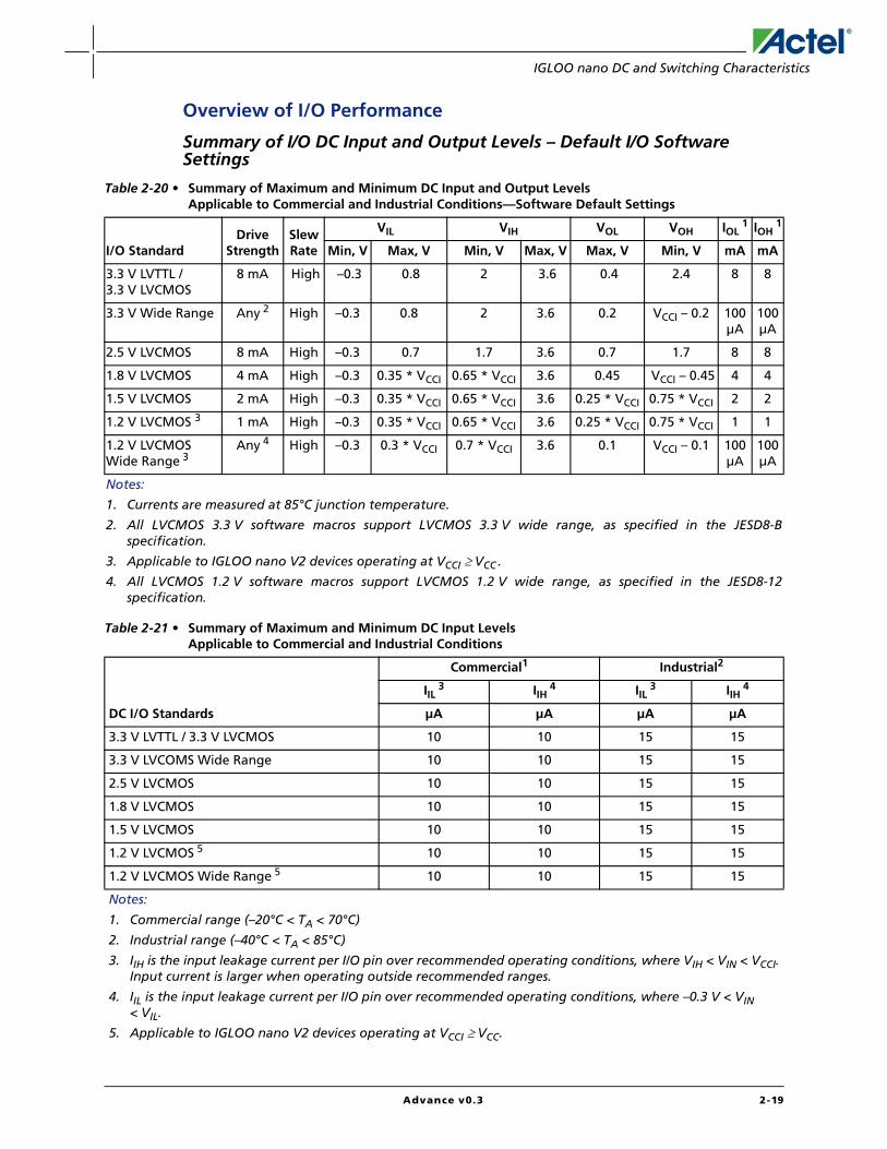
Overview of I/O Performance
Summary of I/O DC Input and Output Levels – Default I/O Software Settings
Table 2-20 • Summary of Maximum and Minimum DC Input and Output Levels Applicable to Commercial and Industrial Conditions—Software Default Settings
I/O StandardDrive
StrengthSlew Rate
VIL VIH VOL VOH IOL1 IOH
1
Min, V Max, V Min, V Max, V Max, V Min, V mA mA
3.3 V LVTTL /3.3 V LVCMOS
8 mA High –0.3 0.8 2 3.6 0.4 2.4 8 8
3.3 V Wide Range Any 2 High –0.3 0.8 2 3.6 0.2 VCCI – 0.2 100µA
100µA
2.5 V LVCMOS 8 mA High –0.3 0.7 1.7 3.6 0.7 1.7 8 8
1.8 V LVCMOS 4 mA High –0.3 0.35 * VCCI 0.65 * VCCI 3.6 0.45 VCCI – 0.45 4 4
1.5 V LVCMOS 2 mA High –0.3 0.35 * VCCI 0.65 * VCCI 3.6 0.25 * VCCI 0.75 * VCCI 2 2
1.2 V LVCMOS 3 1 mA High –0.3 0.35 * VCCI 0.65 * VCCI 3.6 0.25 * VCCI 0.75 * VCCI 1 1
1.2 V LVCMOSWide Range 3
Any 4 High –0.3 0.3 * VCCI 0.7 * VCCI 3.6 0.1 VCCI – 0.1 100µA
100µA
Notes:
1. Currents are measured at 85°C junction temperature.
2. All LVCMOS 3.3 V software macros support LVCMOS 3.3 V wide range, as specified in the JESD8-Bspecification.
3. Applicable to IGLOO nano V2 devices operating at VCCI ≥ VCC .
4. All LVCMOS 1.2 V software macros support LVCMOS 1.2 V wide range, as specified in the JESD8-12specification.
Table 2-21 • Summary of Maximum and Minimum DC Input Levels Applicable to Commercial and Industrial Conditions
DC I/O Standards
Commercial1 Industrial2
IIL3 IIH
4 IIL3 IIH
4
µA µA µA µA
3.3 V LVTTL / 3.3 V LVCMOS 10 10 15 15
3.3 V LVCOMS Wide Range 10 10 15 15
2.5 V LVCMOS 10 10 15 15
1.8 V LVCMOS 10 10 15 15
1.5 V LVCMOS 10 10 15 15
1.2 V LVCMOS 5 10 10 15 15
1.2 V LVCMOS Wide Range 5 10 10 15 15
Notes:
1. Commercial range (–20°C < TA < 70°C)
2. Industrial range (–40°C < TA < 85°C)
3. IIH is the input leakage current per I/O pin over recommended operating conditions, where VIH < VIN < VCCI.Input current is larger when operating outside recommended ranges.
4. IIL is the input leakage current per I/O pin over recommended operating conditions, where –0.3 V < VIN< VIL.
5. Applicable to IGLOO nano V2 devices operating at VCCI ≥ VCC.
Advance v0.3 2-19

IGLOO nano DC and Switching Characteristics
Summary of I/O Timing Characteristics – Default I/O Software Settings
Table 2-22 • Summary of AC Measuring Points
Standard Measuring Trip Point (Vtrip)
3.3 V LVTTL / 3.3 V LVCMOS 1.4 V
3.3 V LVCMOS Wide Range 1.4 V
2.5 V LVCMOS 1.2 V
1.8 V LVCMOS 0.90 V
1.5 V LVCMOS 0.75 V
1.2 V LVCMOS 0.60 V
1.2 V LVCMOS Wide Range 0.60 V
Table 2-23 • I/O AC Parameter Definitions
Parameter Parameter Definition
tDP Data to Pad delay through the Output Buffer
tPY Pad to Data delay through the Input Buffer
tDOUT Data to Output Buffer delay through the I/O interface
tEOUT Enable to Output Buffer Tristate Control delay through the I/O interface
tDIN Input Buffer to Data delay through the I/O interface
tHZ Enable to Pad delay through the Output Buffer—HIGH to Z
tZH Enable to Pad delay through the Output Buffer—Z to HIGH
tLZ Enable to Pad delay through the Output Buffer—LOW to Z
tZL Enable to Pad delay through the Output Buffer—Z to LOW
tZHS Enable to Pad delay through the Output Buffer with delayed enable—Z to HIGH
tZLS Enable to Pad delay through the Output Buffer with delayed enable—Z to LOW
2-20 Advance v0.3

IGLOO nano DC and Switching Characteristics
Applies to IGLOO nano at 1.5 V Core Operating Conditions
Applies to IGLOO nano at 1.2 V Core Operating Conditions
Table 2-24 • Summary of I/O Timing Characteristics—Software Default SettingsSTD Speed Grade, Commercial-Case Conditions: TJ = 70°C, Worst-Case VCC = 1.425 V,Worst-Case VCCI = 3.0 V
I/O
Sta
nd
ard
Dri
ve S
tren
gth
(m
A)
Slew
Rat
e
Cap
acit
ive
Load
(p
F)
t DO
UT
t DP
t DIN
t PY
t PY
S
t EO
UT
t ZL
t ZH
t LZ
t HZ
Un
its
3.3 V LVTTL /3.3 V LVCMOS
8 mA High 5 pF 0.97 1.96 0.19 0.85 1.14 0.66 1.73 1.32 2.04 2.38 ns
3.3 V LVCMOSWide Range
Any 1 High 5 pF TBD TBD TBD TBD TBD TBD TBD TBD TBD TBD TBD
2.5 V LVCMOS 8 mA High 5 pF 0.97 1.99 0.19 1.06 1.22 0.66 1.76 1.42 2.04 2.25 ns
1.8 V LVCMOS 4 mA High 5 pF 0.97 2.30 0.19 0.99 1.43 0.66 2.01 1.64 2.08 2.15 ns
1.5 V LVCMOS 2 mA High 5 pF 0.97 2.65 0.19 1.15 1.62 0.66 2.31 1.85 2.13 2.11 ns
Notes:
1. All LVCMOS 3.3 V software macros support LVCMOS 3.3 V wide range, as specified in the JESD8-Bspecification.
2. For specific junction temperature and voltage supply levels, refer to Table 2-6 on page 2-6 for deratingvalues.
Table 2-25 • Summary of I/O Timing Characteristics—Software Default SettingsSTD Speed Grade, Commercial-Case Conditions: TJ = 70°C, Worst-Case VCC = 1.14 V, Worst-Case VCCI = 3.0 V
I/O
Sta
nd
ard
Dri
ve S
tren
gth
(m
A)
Slew
Rat
e
Cap
acit
ive
Load
(p
F)
t DO
UT
t DP
t DIN
t PY)
t PY
S
t EO
UT
t ZL
t ZH
t LZ
t HZ
Un
its
3.3 V LVTTL /3.3 V LVCMOS
8 mA High 5 pF 1.55 2.81 0.26 0.99 1.14 1.10 2.53 2.01 2.48 3.10 ns
3.3 V LVCMOSWide Range
Any 1 High 5 pF TBD TBD TBD TBD TBD TBD TBD TBD TBD TBD ns
2.5 V LVCMOS 8 mA High 5 pF 1.55 2.82 0.26 1.20 1.22 1.10 2.53 2.15 2.46 2.93 ns
1.8 V LVCMOS 4 mA High 5 pF 1.55 3.11 0.26 1.12 1.43 1.10 2.76 2.46 2.49 2.75 ns
1.5 V LVCMOS 2 mA High 5 pF 1.55 3.50 0.26 1.26 1.62 1.10 3.09 2.76 2.53 2.67 ns
1.2 V LVCMOS 1 mA High 5 pF 1.55 4.47 0.26 1.56 1.66 1.10 3.56 3.18 3.00 3.25 ns
1.2 V LVCMOSWide Range
100 µA High 5 pF TBD TBD TBD TBD TBD TBD TBD TBD TBD TBD ns
Notes:
1. All LVCMOS 3.3 V software macros support LVCMOS 3.3 V wide range, as specified in the JESD8-Bspecification.
2. For specific junction temperature and voltage supply levels, refer to Table 2-6 on page 2-6 for deratingvalues.
Advance v0.3 2-21

IGLOO nano DC and Switching Characteristics
Detailed I/O DC Characteristics
Table 2-26 • Input Capacitance
Symbol Definition Conditions Min. Max. Units
CIN Input capacitance VIN = 0, f = 1.0 MHz 8 pF
CINCLK Input capacitance on the clock pin VIN = 0, f = 1.0 MHz 8 pF
Table 2-27 • I/O Output Buffer Maximum Resistances 1
Standard Drive StrengthRPULL-DOWN
(Ω)2RPULL-UP
(Ω)3
3.3 V LVTTL / 3.3V LVCMOS 2 mA 100 300
4 mA 100 300
6 mA 50 150
8 mA 50 150
3.3 V LVCMOS Wide Range 100 µA TBD TBD
2.5 V LVCMOS 2 mA 100 200
4 mA 100 200
6 mA 50 100
8 mA 50 100
1.8 V LVCMOS 2 mA 200 225
4 mA 100 112
1.5 V LVCMOS 2 mA 200 224
1.2 V LVCMOS 4 2 mA TBD TBD
1.2 V LVCMOS Wide Range 4 100 µA TBD TBD
Notes:
1. These maximum values are provided for informational reasons only. Minimum output buffer resistancevalues depend on VCCI, drive strength selection, temperature, and process. For board design considerationsand detailed output buffer resistances, use the corresponding IBIS models located on the Actel website athttp://www.actel.com/download/ibis/default.aspx.
2. R(PULL-DOWN-MAX) = (VOLspec) / IOLspec
3. R(PULL-UP-MAX) = (VCCImax – VOHspec) / IOHspec
4. Applicable to IGLOO nano V2 devices operating at VCCI ≥ VCC.
2-22 Advance v0.3

IGLOO nano DC and Switching Characteristics
Table 2-28 • I/O Weak Pull-Up/Pull-Down ResistancesMinimum and Maximum Weak Pull-Up/Pull-Down Resistance Values
VCCI
R(WEAK PULL-UP)1
(Ω)R(WEAK PULL-DOWN)
2
(Ω)
Min. Max. Min. Max.
3.3 V 10 k 45 k 10 k 45 k
2.5 V 11 k 55 k 12 k 74 k
1.8 V 18 k 70 k 17 k 110 k
1.5 V 19 k 90 k 19 k 140 k
1.2 V 25 k 110 k 25 k 150 k
Notes:
1. R(WEAK PULL-UP-MAX) = (VOLspec) / I(WEAK PULL-UP-MIN)
2. R(WEAK PULL-UP-MAX) = (VCCImax – VOHspec) / I(WEAK PULL-UP-MIN)
Table 2-29 • I/O Short Currents IOSH/IOSL
Drive Strength IOSL (mA)* IOSH (mA)*
3.3 V LVTTL / 3.3 V LVCMOS 2 mA 25 27
4 mA 25 27
6 mA 51 54
8 mA 51 54
3.3 V LVCMOS Wide Range 100 µA TBD TBD
2.5 V LVCMOS 2 mA 16 18
4 mA 16 18
6 mA 32 37
8 mA 32 37
1.8 V LVCMOS 2 mA 9 11
4 mA 17 22
1.5 V LVCMOS 2 mA 13 16
1.2 V LVCMOS 1 mA TBD TBD
1.2 V LVCMOS Wide Range 100 µA TBD TBD
* TJ = 100°C
Advance v0.3 2-23

IGLOO nano DC and Switching Characteristics
The length of time an I/O can withstand IOSH/IOSL events depends on the junction temperature. Thereliability data below is based on a 3.3 V, 8 mA I/O setting, which is the worst case for this type ofanalysis.
For example, at 110°C, the short current condition would have to be sustained for more than threemonths to cause a reliability concern. The I/O design does not contain any short circuit protection,but such protection would only be needed in extremely prolonged stress conditions.
Table 2-30 • Duration of Short Circuit Event before Failure
Temperature Time before Failure
–40°C > 20 years
–20°C > 20 years
0°C > 20 years
25°C > 20 years
70°C 5 years
85°C 2 years
100°C 6 months
110°C 3 months
Table 2-31 • Schmitt Trigger Input HysteresisHysteresis Voltage Value (Typ.) for Schmitt Mode Input Buffers
Input Buffer Configuration Hysteresis Value (typ.)
3.3 V LVTTL / LVCMOS (Schmitt trigger mode) 240 mV
2.5 V LVCMOS (Schmitt trigger mode) 140 mV
1.8 V LVCMOS (Schmitt trigger mode) 80 mV
1.5 V LVCMOS (Schmitt trigger mode) 60 mV
1.2 V LVCMOS (Schmitt trigger mode) 40 mV
Table 2-32 • I/O Input Rise Time, Fall Time, and Related I/O Reliability
Input BufferInput Rise/Fall Time
(min.)Input Rise/Fall Time
(max.) Reliability
LVTTL/LVCMOS (Schmitt triggerdisabled)
No requirement 10 ns * 20 years (100°C)
LVTTL/LVCMOS (Schmitt triggerenabled)
No requirement No requirement, but input noise voltage
cannot exceed Schmitt hysteresis.
20 years (100°C)
* The maximum input rise/fall time is related to the noise induced into the input buffer trace. If thenoise is low, then the rise time and fall time of input buffers can be increased beyond themaximum value. The longer the rise/fall times, the more susceptible the input signal is to theboard noise. Actel recommends signal integrity evaluation/characterization of the system toensure that there is no excessive noise coupling into input signals.
2-24 Advance v0.3

IGLOO nano DC and Switching Characteristics
Single-Ended I/O Characteristics
3.3 V LVTTL / 3.3 V LVCMOSLow-Voltage Transistor–Transistor Logic (LVTTL) is a general-purpose standard (EIA/JESD) for 3.3 Vapplications. It uses an LVTTL input buffer and push-pull output buffer.
Table 2-33 • Minimum and Maximum DC Input and Output Levels
3.3 V LVTTL /3.3 V LVCMOS VIL VIH VOL VOH IOL IOH IOSL IOSH IIL
1 IIH2
DriveStrength Min., V Max., V Min., V Max., V Max., V Min., V mA mA Max., mA3 Max., mA3 µA4 µA4
2 mA –0.3 0.8 2 3.6 0.4 2.4 2 2 25 27 10 10
4 mA –0.3 0.8 2 3.6 0.4 2.4 4 4 25 27 10 10
6 mA –0.3 0.8 2 3.6 0.4 2.4 6 6 51 54 10 10
8 mA –0.3 0.8 2 3.6 0.4 2.4 8 8 51 54 10 10
Notes:
1. IIL is the input leakage current per I/O pin over recommended operating conditions where –0.3 < VIN < VIL.
2. IIH is the input leakage current per I/O pin over recommended operating conditions where VIH < VIN < VCCI.Input current is larger when operating outside recommended ranges.
3. Currents are measured at high temperature (100°C junction temperature) and maximum voltage.
4. Currents are measured at 85°C junction temperature.
5. Software default selection highlighted in gray.
Figure 2-7 • AC Loading
Table 2-34 • 3.3 V LVTTL/LVCMOS AC Waveforms, Measuring Points, and Capacitive Loads
Input LOW (V) Input HIGH (V) Measuring Point* (V) CLOAD (pF)
0 3.3 1.4 5
* Measuring point = Vtrip. See Table 2-22 on page 2-20 for a complete table of trip points.
Test PointTest Point
Enable PathDatapath 5 pF
R = 1 k R to VCCI for tLZ/tZL/tZLSR to GND for tHZ/tZH/tZHS
35 pF for tZH/tZHS/tZL/tZLS5 pF for tHZ/tLZ
Advance v0.3 2-25

IGLOO nano DC and Switching Characteristics
Timing Characteristics
Applies to 1.5 V DC Core Voltage
Table 2-35 • 3.3 V LVTTL / 3.3 V LVCMOS Low Slew – Applies to 1.5 V DC Core VoltageCommercial-Case Conditions: TJ = 70°C, Worst-Case VCC = 1.425 V, Worst-Case VCCI = 3.0 V
Drive Strength Speed Grade tDOUT tDP tDIN tPY tPYS tEOUT tZL tZH tLZ tHZ Units
2 mA STD 0.97 3.94 0.19 0.85 1.14 0.66 3.39 2.95 1.82 1.87 ns
4 mA STD 0.97 3.94 0.19 0.85 1.14 0.66 3.39 2.95 1.82 1.87 ns
6 mA STD 0.97 3.20 0.19 0.85 1.14 0.66 2.88 2.65 2.04 2.27 ns
8 mA STD 0.97 3.20 0.19 0.85 1.14 0.66 2.88 2.65 2.04 2.27 ns
Note: For specific junction temperature and voltage supply levels, refer to Table 2-6 on page 2-6 for deratingvalues.
Table 2-36 • 3.3 V LVTTL / 3.3 V LVCMOS High Slew – Applies to 1.5 V DC Core VoltageCommercial-Case Conditions: TJ = 70°C, Worst-Case VCC = 1.425 V, Worst-Case VCCI = 3.0 V
Drive Strength Speed Grade tDOUT tDP tDIN tPY tPYS tEOUT tZL tZH tLZ tHZ Units
2 mA STD 0.97 2.35 0.19 0.85 1.14 0.66 1.88 1.43 1.81 1.98 ns
4 mA STD 0.97 2.35 0.19 0.85 1.14 0.66 1.88 1.43 1.81 1.98 ns
6 mA STD 0.97 1.96 0.19 0.85 1.14 0.66 1.73 1.32 2.04 2.38 ns
8 mA STD 0.97 1.96 0.19 0.85 1.14 0.66 1.73 1.32 2.04 2.38 ns
Notes:
1. Software default selection highlighted in gray.
2. For specific junction temperature and voltage supply levels, refer to Table 2-6 on page 2-6 for deratingvalues.
2-26 Advance v0.3

IGLOO nano DC and Switching Characteristics
Applies to 1.2 V DC Core Voltage
Table 2-37 • 3.3 V LVTTL / 3.3 V LVCMOS Low Slew – Applies to 1.2 V DC Core VoltageCommercial-Case Conditions: TJ = 70°C, Worst-Case VCC = 1.14 V, Worst-Case VCCI = 3.0 V
Drive Strength Speed Grade tDOUT tDP tDIN tPY tPYS tEOUT tZL tZH tLZ tHZ Units
2 mA STD 1.55 5.23 0.26 0.99 1.14 1.10 4.56 3.93 2.25 2.56 ns
4 mA STD 1.55 5.23 0.26 0.99 1.14 1.10 4.56 3.93 2.25 2.56 ns
6 mA STD 1.55 4.21 0.26 0.99 1.14 1.10 3.81 3.42 2.48 2.97 ns
8 mA STD 1.55 4.21 0.26 0.99 1.14 1.10 3.81 3.42 2.48 2.97 ns
Note: For specific junction temperature and voltage supply levels, refer to Table 2-6 on page 2-6 for deratingvalues.
Table 2-38 • 3.3 V LVTTL / 3.3 V LVCMOS High Slew – Applies to 1.2 V DC Core VoltageCommercial-Case Conditions: TJ = 70°C, Worst-Case VCC = 1.14 V, Worst-Case VCCI = 3.0 V
Drive Strength Speed Grade tDOUT tDP tDIN tPY tPYS tEOUT tZL tZH tLZ tHZ Units
2 mA STD 1.55 3.49 0.26 0.99 1.14 1.10 2.91 2.33 2.24 2.68 ns
4 mA STD 1.55 3.49 0.26 0.99 1.14 1.10 2.91 2.33 2.24 2.68 ns
6 mA STD 1.55 2.81 0.26 0.99 1.14 1.10 2.53 2.01 2.48 3.10 ns
8 mA STD 1.55 2.81 0.26 0.99 1.14 1.10 2.53 2.01 2.48 3.10 ns
Notes:
1. Software default selection highlighted in gray.
2. For specific junction temperature and voltage supply levels, refer to Table 2-6 on page 2-6 for deratingvalues.
Advance v0.3 2-27

IGLOO nano DC and Switching Characteristics
3.3 V LVCOMOS Wide Range
Table 2-39 • Minimum and Maximum DC Input and Output Levels for LVCMOS 3.3 V Wide Range
3.3 V LVCMOSWide Range VIL VIH VOL VOH IOL IOH IIL
1 IIH2
DriveStrength Min., V Max., V Min., V Max., V Max., V Min., V µA µA µA3 µA3
All 4 –0.3 0.8 2 3.6 0.2 VDD – 0.2 100 100 10 10
Notes:
1. IIL is the input leakage current per I/O pin over recommended operating conditions where –0.3 < VIN < VIL.
2. IIH is the input leakage current per I/O pin over recommended operating conditions where VIH < VIN < VCCI.Input current is larger when operating outside recommended ranges.
3. Currents are measured at 85°C junction temperature.
4. All LVCMOS 3.3 V software macros support LVCMOS 3.3 V Wide Range, as specified in the JEDEC JESD8-Bspecification.
2-28 Advance v0.3

IGLOO nano DC and Switching Characteristics
2.5 V LVCMOSLow-Voltage CMOS for 2.5 V is an extension of the LVCMOS standard (JESD8-5) used for general-purpose 2.5 V applications. It uses a 5 V–tolerant input buffer and push-pull output buffer.
Table 2-40 • Minimum and Maximum DC Input and Output Levels
2.5 VLVCMOS VIL VIH VOL VOH IOL IOH IOSL IOSH IIL
1 IIH2
DriveStrength Min., V Max., V Min., V Max., V Max., V Min., V mA mA Max., mA3 Max., mA3 µA4 µA4
2 mA –0.3 0.7 1.7 3.6 0.7 1.7 2 2 16 18 10 10
4 mA –0.3 0.7 1.7 3.6 0.7 1.7 4 4 16 18 10 10
6 mA –0.3 0.7 1.7 3.6 0.7 1.7 6 6 32 37 10 10
8 mA –0.3 0.7 1.7 3.6 0.7 1.7 8 8 32 37 10 10
Notes:
1. IIL is the input leakage current per I/O pin over recommended operating conditions where –0.3 < VIN < VIL.
2. IIH is the input leakage current per I/O pin over recommended operating conditions where VIH < VIN < VCCI.Input current is larger when operating outside recommended ranges.
3. Currents are measured at high temperature (100°C junction temperature) and maximum voltage.
4. Currents are measured at 85°C junction temperature.
5. Software default selection highlighted in gray.
Figure 2-8 • AC Loading
Table 2-41 • 2.5 V LVCMOS AC Waveforms, Measuring Points, and Capacitive Loads
Input LOW (V) Input HIGH (V) Measuring Point* (V) CLOAD (pF)
0 2.5 1.2 5
* Measuring point = Vtrip. See Table 2-22 on page 2-20 for a complete table of trip points.
Test PointTest Point
Enable PathDatapath 5 pF
R = 1 k R to VCCI for tLZ/tZL/tZLSR to GND for tHZ/tZH/tZHS
35 pF for tZH/tZHS/tZL/tZLS5 pF for tHZ/tLZ
Advance v0.3 2-29

IGLOO nano DC and Switching Characteristics
Timing Characteristics
Applies to 1.5 V DC Core Voltage
Table 2-42 • 2.5 V LVCMOS Low Slew – Applies to 1.5 V DC Core VoltageCommercial-Case Conditions: TJ = 70°C, Worst-Case VCC = 1.425 V, Worst-Case VCCI = 2.3 V
Drive Strength Speed Grade tDOUT tDP tDIN tPY tPYS tEOUT tZL tZH tLZ tHZ Units
2 mA STD 0.97 4.44 0.19 1.06 1.22 0.66 3.87 3.47 1.80 1.70 ns
4 mA STD 0.97 4.44 0.19 1.06 1.22 0.66 3.87 3.47 1.80 1.70 ns
8 mA STD 0.97 3.61 0.19 1.06 1.22 0.66 3.27 3.11 2.05 2.17 ns
8 mA STD 0.97 3.61 0.19 1.06 1.22 0.66 3.27 3.11 2.05 2.17 ns
Note: For specific junction temperature and voltage supply levels, refer to Table 2-6 on page 2-6 for deratingvalues.
Table 2-43 • 2.5 V LVCMOS High Slew – Applies to 1.5 V DC Core VoltageCommercial-Case Conditions: TJ = 70°C, Worst-Case VCC = 1.425 V, Worst-Case VCCI = 2.3 V
Drive Strength Speed Grade tDOUT tDP tDIN tPY tPYS tEOUT tZL tZH tLZ tHZ Units
2 mA STD 0.97 2.41 0.19 1.06 1.22 0.66 1.93 1.57 1.79 1.77 ns
4 mA STD 0.97 2.41 0.19 1.06 1.22 0.66 1.93 1.57 1.79 1.77 ns
6 mA STD 0.97 1.99 0.19 1.06 1.22 0.66 1.76 1.42 2.04 2.25 ns
8 mA STD 0.97 1.99 0.19 1.06 1.22 0.66 1.76 1.42 2.04 2.25 ns
Notes:
1. Software default selection highlighted in gray.
2. For specific junction temperature and voltage supply levels, refer to Table 2-6 on page 2-6 for deratingvalues.
2-30 Advance v0.3

IGLOO nano DC and Switching Characteristics
Applies to 1.2 V DC Core Voltage
Table 2-44 • 2.5 LVCMOS Low Slew – Applies to 1.2 V DC Core VoltageCommercial-Case Conditions: TJ = 70°C, Worst-Case VCC = 1.14 V, Worst-Case VCCI = 2.3 V
Drive Strength Speed Grade tDOUT tDP tDIN tPY tPYS tEOUT tZL tZH tLZ tHZ Units
2 mA STD 1.55 5.75 0.26 1.20 1.22 1.10 5.05 4.57 2.21 2.35 ns
4 mA STD 1.55 5.75 0.26 1.20 1.22 1.10 5.05 4.57 2.21 2.35 ns
6 mA STD 1.55 4.63 0.26 1.20 1.22 1.10 4.21 3.94 2.47 2.83 ns
8 mA STD 1.55 4.63 0.26 1.20 1.22 1.10 4.21 3.94 2.47 2.83 ns
Note: For specific junction temperature and voltage supply levels, refer to Table 2-6 on page 2-6 for deratingvalues.
Table 2-45 • 2.5 V LVCMOS High Slew – Applies to 1.2 V DC Core VoltageCommercial-Case Conditions: TJ = 70°C, Worst-Case VCC = 1.14 V, Worst-Case VCCI = 2.3 V
Drive Strength Speed Grade tDOUT tDP tDIN tPY tPYS tEOUT tZL tZH tLZ tHZ Units
2 mA STD 1.55 3.52 0.26 1.20 1.22 1.10 2.94 2.60 2.21 2.44 ns
4 mA STD 1.55 3.52 0.26 1.20 1.22 1.10 2.94 2.60 2.21 2.44 ns
6 mA STD 1.55 2.82 0.26 1.20 1.22 1.10 2.53 2.15 2.46 2.93 ns
8 mA STD 1.55 2.82 0.26 1.20 1.22 1.10 2.53 2.15 2.46 2.93 ns
Notes:
1. Software default selection highlighted in gray.
2. For specific junction temperature and voltage supply levels, refer to Table 2-6 on page 2-6 for deratingvalues.
Advance v0.3 2-31

IGLOO nano DC and Switching Characteristics
1.8 V LVCMOSLow-voltage CMOS for 1.8 V is an extension of the LVCMOS standard (JESD8-5) used for general-purpose 1.8 V applications. It uses a 1.8 V input buffer and a push-pull output buffer.
Table 2-46 • Minimum and Maximum DC Input and Output Levels
1.8 VLVCMOS VIL VIH VOL VOH IOL IOH IOSL IOSH IIL
1 IIH2
DriveStrength Min., V Max., V Min., V Max., V Max., V Min., V mA mA Max., mA3 Max., mA3 µA4 µA4
2 mA –0.3 0.35 * VCCI 0.65 * VCCI 3.6 0.45 VCCI – 0.45 2 2 9 11 10 10
4 mA –0.3 0.35 * VCCI 0.65 * VCCI 3.6 0.45 VCCI – 0.45 4 4 17 22 10 10
Notes:
1. IIL is the input leakage current per I/O pin over recommended operating conditions where –0.3 < VIN < VIL.
2. IIH is the input leakage current per I/O pin over recommended operating conditions where VIH < VIN < VCCI.Input current is larger when operating outside recommended ranges.
3. Currents are measured at high temperature (100°C junction temperature) and maximum voltage.
4. Currents are measured at 85°C junction temperature.
5. Software default selection highlighted in gray.
Figure 2-9 • AC Loading
Table 2-47 • 1.8 V LVCMOS AC Waveforms, Measuring Points, and Capacitive Loads
Input LOW (V) Input HIGH (V) Measuring Point* (V) CLOAD (pF)
0 1.8 0.9 5
* Measuring point = Vtrip. See Table 2-22 on page 2-20 for a complete table of trip points.
Test PointTest Point
Enable PathDatapath 5 pF
R = 1 k R to VCCI for tLZ/tZL/tZLSR to GND for tHZ/tZH/tZHS
35 pF for tZH/tZHS/tZL/tZLS5 pF for tHZ/tLZ
2-32 Advance v0.3

IGLOO nano DC and Switching Characteristics
Timing Characteristics
Applies to 1.5 V DC Core Voltage
Applies to 1.2 V DC Core Voltage
Table 2-48 • 1.8 V LVCMOS Low Slew – Applies to 1.5 V DC Core VoltageCommercial-Case Conditions: TJ = 70°C, Worst-Case VCC = 1.425 V, Worst-Case VCCI = 1.7 V
Drive Strength Speed Grade tDOUT tDP tDIN tPY tPYS tEOUT tZL tZH tLZ tHZ Units
2 mA STD 0.97 5.89 0.19 0.99 1.43 0.66 5.20 4.48 1.78 1.30 ns
4 mA STD 0.97 4.82 0.19 0.99 1.43 0.66 4.39 4.04 2.08 2.07 ns
Note: For specific junction temperature and voltage supply levels, refer to Table 2-6 on page 2-6 for deratingvalues.
Table 2-49 • 1.8 V LVCMOS High Slew – Applies to 1.5 V DC Core VoltageCommercial-Case Conditions: TJ = 70°C, Worst-Case VCC = 1.425 V, Worst-Case VCCI = 1.7 V
Drive Strength Speed Grade tDOUT tDP tDIN tPY tPYS tEOUT tZL tZH tLZ tHZ Units
2 mA STD 0.97 2.82 0.19 0.99 1.43 0.66 2.25 1.86 1.78 1.35 ns
4 mA STD 0.97 2.30 0.19 0.99 1.43 0.66 2.01 1.64 2.08 2.15 ns
Notes:
1. Software default selection highlighted in gray.
2. For specific junction temperature and voltage supply levels, refer to Table 2-6 on page 2-6 for deratingvalues.
Table 2-50 • 1.8 V LVCMOS Low Slew – Applies to 1.2 V DC Core VoltageCommercial-Case Conditions: TJ = 70°C, Worst-Case VCC = 1.14 V, Worst-Case VCCI = 1.7 V
Drive Strength Speed Grade tDOUT tDP tDIN tPY tPYS tEOUT tZL tZH tLZ tHZ Units
2 mA STD 1.55 7.30 0.26 1.12 1.43 1.10 6.45 5.82 2.18 1.87 ns
4 mA STD 1.55 5.88 0.26 1.12 1.43 1.10 5.35 4.98 2.49 2.67 ns
Note: For specific junction temperature and voltage supply levels, refer to Table 2-6 on page 2-6 for deratingvalues.
Table 2-51 • 1.8 V LVCMOS High Slew – Applies to 1.2 V DC Core VoltageCommercial-Case Conditions: TJ = 70°C, Worst-Case VCC = 1.14 V, Worst-Case VCCI = 1.7 V
Drive Strength Speed Grade tDOUT tDP tDIN tPY tPYS tEOUT tZL tZH tLZ tHZ Units
2 mA STD 1.55 4.24 0.26 1.12 1.43 1.10 3.28 3.11 2.18 1.92 ns
4 mA STD 1.55 3.11 0.26 1.12 1.43 1.10 2.76 2.46 2.49 2.75 ns
Notes:
1. Software default selection highlighted in gray.
2. For specific junction temperature and voltage supply levels, refer to Table 2-6 on page 2-6 for deratingvalues.
Advance v0.3 2-33
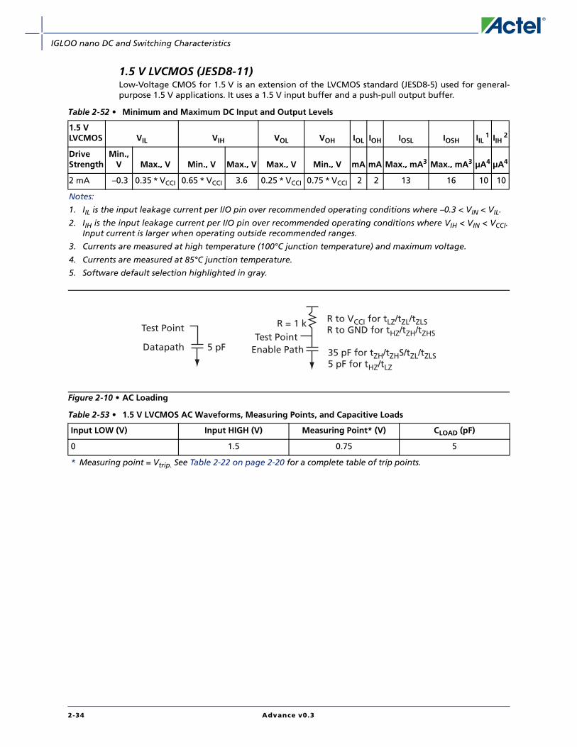
IGLOO nano DC and Switching Characteristics
1.5 V LVCMOS (JESD8-11)Low-Voltage CMOS for 1.5 V is an extension of the LVCMOS standard (JESD8-5) used for general-purpose 1.5 V applications. It uses a 1.5 V input buffer and a push-pull output buffer.
Table 2-52 • Minimum and Maximum DC Input and Output Levels
1.5 VLVCMOS VIL VIH VOL VOH IOL IOH IOSL IOSH IIL
1 IIH2
DriveStrength
Min.,V Max., V Min., V Max., V Max., V Min., V mA mA Max., mA3 Max., mA3 µA4 µA4
2 mA –0.3 0.35 * VCCI 0.65 * VCCI 3.6 0.25 * VCCI 0.75 * VCCI 2 2 13 16 10 10
Notes:
1. IIL is the input leakage current per I/O pin over recommended operating conditions where –0.3 < VIN < VIL.
2. IIH is the input leakage current per I/O pin over recommended operating conditions where VIH < VIN < VCCI.Input current is larger when operating outside recommended ranges.
3. Currents are measured at high temperature (100°C junction temperature) and maximum voltage.
4. Currents are measured at 85°C junction temperature.
5. Software default selection highlighted in gray.
Figure 2-10 • AC Loading
Table 2-53 • 1.5 V LVCMOS AC Waveforms, Measuring Points, and Capacitive Loads
Input LOW (V) Input HIGH (V) Measuring Point* (V) CLOAD (pF)
0 1.5 0.75 5
* Measuring point = Vtrip. See Table 2-22 on page 2-20 for a complete table of trip points.
Test PointTest Point
Enable PathDatapath 5 pF
R = 1 k R to VCCI for tLZ/tZL/tZLSR to GND for tHZ/tZH/tZHS
35 pF for tZH/tZHS/tZL/tZLS5 pF for tHZ/tLZ
2-34 Advance v0.3

IGLOO nano DC and Switching Characteristics
Timing Characteristics
Applies to 1.5 V DC Core Voltage
Applies to 1.2 V DC Core Voltage
Table 2-54 • 1.5 V LVCMOS Low Slew – Applies to 1.5 V DC Core VoltageCommercial-Case Conditions: TJ = 70°C, Worst-Case VCC = 1.425 V, Worst-Case VCCI = 1.4 V
Drive Strength Speed Grade tDOUT tDP tDIN tPY tPYS tEOUT tZL tZH tLZ tHZ Units
2 mA STD 0.97 6.07 0.19 1.15 1.62 0.66 5.57 4.89 2.13 2.02 ns
Note: For specific junction temperature and voltage supply levels, refer to Table 2-6 on page 2-6 for deratingvalues.
Table 2-55 • 1.5 V LVCMOS High Slew – Applies to 1.5 V DC Core VoltageCommercial-Case Conditions: TJ = 70°C, Worst-Case VCC = 1.425 V, Worst-Case VCCI = 1.4 V
Drive Strength Speed Grade tDOUT tDP tDIN tPY tPYS tEOUT tZL tZH tLZ tHZ Units
2 mA STD 0.97 2.65 0.19 1.15 1.62 0.66 2.31 1.85 2.13 2.11 ns
Notes:
1. Software default selection highlighted in gray.
2. For specific junction temperature and voltage supply levels, refer to Table 2-6 on page 2-6 for deratingvalues.
Table 2-56 • 1.5 V LVCMOS Low Slew – Applies to 1.2 V DC Core VoltageCommercial-Case Conditions: TJ = 70°C, Worst-Case VCC = 1.14 V, Worst-Case VCCI = 1.4 V
Drive Strength Speed Grade tDOUT tDP tDIN tPY tPYS tEOUT tZL tZH tLZ tHZ Units
2 mA STD 1.55 7.23 0.26 1.26 1.62 1.10 6.61 5.94 2.53 2.58 ns
Note: For specific junction temperature and voltage supply levels, refer to Table 2-6 on page 2-6 for deratingvalues.
Table 2-57 • 1.5 V LVCMOS High Slew – Applies to 1.2 V DC Core VoltageCommercial-Case Conditions: TJ = 70°C, Worst-Case VCC = 1.14 V, Worst-Case VCCI = 1.4 V
Drive Strength Speed Grade tDOUT tDP tDIN tPY tPYS tEOUT tZL tZH tLZ tHZ Units
2 mA STD 1.55 3.50 0.26 1.26 1.62 1.10 3.09 2.76 2.53 2.67 ns
Notes:
1. Software default selection highlighted in gray.
2. For specific junction temperature and voltage supply levels, refer to Table 2-6 on page 2-6 for deratingvalues.
Advance v0.3 2-35

IGLOO nano DC and Switching Characteristics
1.2 V LVCMOS (JESD8-12A)Low-Voltage CMOS for 1.2 V complies with the LVCMOS standard JESD8-12A for general purpose1.2 V applications. It uses a 1.2 V input buffer and a push-pull output buffer.
Timing Characteristics
Applies to 1.2 V DC Core Voltage
Table 2-58 • Minimum and Maximum DC Input and Output Levels
1.2 VLVCMOS VIL VIH VOL VOH IOL IOH IOSL IOSH IIL
1 IIH2
DriveStrength
Min.,V
Max.,V Min., V Max., V Max., V Min., V mA mA Max., mA3 Max., mA3 µA4 µA4
1 mA –0.3 0.35 * VCCI 0.65 * VCCI 3.6 0.25 * VCCI 0.75 * VCCI 1 1 TBD TBD 10 10
Notes:
1. IIL is the input leakage current per I/O pin over recommended operating conditions where –0.3 < VIN < VIL.
2. IIH is the input leakage current per I/O pin over recommended operating conditions where VIH < VIN < VCCI.Input current is larger when operating outside recommended ranges.
3. Currents are measured at high temperature (100°C junction temperature) and maximum voltage.
4. Currents are measured at 85°C junction temperature.
5. Software default selection highlighted in gray.
Figure 2-11 • AC Loading
Table 2-59 • 1.2 V LVCMOS AC Waveforms, Measuring Points, and Capacitive Loads
Input LOW (V) Input HIGH (V) Measuring Point* (V) CLOAD (pF)
0 1.2 0.6 5
* Measuring point = Vtrip. See Table 2-22 on page 2-20 for a complete table of trip points.
Test PointTest Point
Enable PathDatapath 5 pF
R = 1 k R to VCCI for tLZ/tZL/tZLSR to GND for tHZ/tZH/tZHS
35 pF for tZH/tZHS/tZL/tZLS5 pF for tHZ/tLZ
Table 2-60 • 1.2 V LVCMOS Low Slew Commercial-Case Conditions: TJ = 70°C, Worst-Case VCC = 1.14 V, Worst-Case VCCI = 1.14 V
Drive Strength Speed Grade tDOUT tDP tDIN tPY tPYS tEOUT tZL tZH tLZ tHZ Units
1 mA STD 1.55 10.33 0.26 1.56 1.66 1.10 8.52 7.30 3.00 3.12 ns
Note: For specific junction temperature and voltage supply levels, refer to Table 2-6 on page 2-6 for deratingvalues.
Table 2-61 • 1.2 V LVCMOS High Slew Commercial-Case Conditions: TJ = 70°C, Worst-Case VCC = 1.14 V, Worst-Case VCCI = 1.14 V
Drive Strength Speed Grade tDOUT tDP tDIN tPY tPYS tEOUT tZL tZH tLZ tHZ Units
1 mA STD 1.55 4.47 0.26 1.56 1.66 1.10 3.56 3.18 3.00 3.25 ns
Note: For specific junction temperature and voltage supply levels, refer to Table 2-6 on page 2-6 for deratingvalues.
2-36 Advance v0.3

IGLOO nano DC and Switching Characteristics
I/O Register Specifications
Fully Registered I/O Buffers with Asynchronous Preset
Figure 2-12 • Timing Model of Registered I/O Buffers with Asynchronous Preset
INB
UF
INB
UF
TRIB
UF
CLK
BU
F
INBUFCLKBUF
Data Input I/O Register with: Active High Preset Positive-Edge Triggered
Data Output Register andEnable Output Register with: Active High Preset Postive-Edge Triggered
Pad O
ut
CLK
Preset
Data_out
Data
EOUT
DOUT
CLK
D QDFN1P1
PRE
D Q
DFN1P1
PRE
D QDFN1P1
PRE
D_E
nab
le
A
C
D
E F
H
I
J
L
YCoreArray
Advance v0.3 2-37

IGLOO nano DC and Switching Characteristics
Table 2-62 • Parameter Definition and Measuring Nodes
Parameter Name Parameter DefinitionMeasuring Nodes
(from, to)*
tOCLKQ Clock-to-Q of the Output Data Register H, DOUT
tOSUD Data Setup Time for the Output Data Register F, H
tOHD Data Hold Time for the Output Data Register F, H
tOPRE2Q Asynchronous Preset-to-Q of the Output Data Register L, DOUT
tOREMPRE Asynchronous Preset Removal Time for the Output Data Register L, H
tORECPRE Asynchronous Preset Recovery Time for the Output Data Register L, H
tOECLKQ Clock-to-Q of the Output Enable Register H, EOUT
tOESUD Data Setup Time for the Output Enable Register J, H
tOEHD Data Hold Time for the Output Enable Register J, H
tOEPRE2Q Asynchronous Preset-to-Q of the Output Enable Register I, EOUT
tOEREMPRE Asynchronous Preset Removal Time for the Output Enable Register I, H
tOERECPRE Asynchronous Preset Recovery Time for the Output Enable Register I, H
tICLKQ Clock-to-Q of the Input Data Register A, E
tISUD Data Setup Time for the Input Data Register C, A
tIHD Data Hold Time for the Input Data Register C, A
tIPRE2Q Asynchronous Preset-to-Q of the Input Data Register D, E
tIREMPRE Asynchronous Preset Removal Time for the Input Data Register D, A
tIRECPRE Asynchronous Preset Recovery Time for the Input Data Register D, A
* See Figure 2-12 on page 2-37 for more information.
2-38 Advance v0.3

IGLOO nano DC and Switching Characteristics
Fully Registered I/O Buffers with Asynchronous Clear
Figure 2-13 • Timing Model of the Registered I/O Buffers with Asynchronous Clear
CLK
Pad O
ut
CLK
CLR
Data_outData
Y
AA
EOUT
DOUT
Core
ArrayD Q
DFN1C1
CLR
D Q
DFN1C1
CLR
D Q
DFN1C1
CLR
D_E
nab
le
CC
DD
EE
FF
LL
HH
JJ
CLK
BU
FIN
BU
F
TRIB
UF
INBUF CLKBUF
INB
UF
Data Input I/O Register with Active High Clear Positive-Edge Triggered
Data Output Register andEnable Output Register with Active High Clear Positive-Edge Triggered
Advance v0.3 2-39

IGLOO nano DC and Switching Characteristics
Table 2-63 • Parameter Definition and Measuring Nodes
Parameter Name Parameter DefinitionMeasuring Nodes
(from, to)*
tOCLKQ Clock-to-Q of the Output Data Register HH, DOUT
tOSUD Data Setup Time for the Output Data Register FF, HH
tOHD Data Hold Time for the Output Data Register FF, HH
tOCLR2Q Asynchronous Clear-to-Q of the Output Data Register LL, DOUT
tOREMCLR Asynchronous Clear Removal Time for the Output Data Register LL, HH
tORECCLR Asynchronous Clear Recovery Time for the Output Data Register LL, HH
tOECLKQ Clock-to-Q of the Output Enable Register HH, EOUT
tOESUD Data Setup Time for the Output Enable Register JJ, HH
tOEHD Data Hold Time for the Output Enable Register JJ, HH
tOECLR2Q Asynchronous Clear-to-Q of the Output Enable Register II, EOUT
tOEREMCLR Asynchronous Clear Removal Time for the Output Enable Register II, HH
tOERECCLR Asynchronous Clear Recovery Time for the Output Enable Register II, HH
tICLKQ Clock-to-Q of the Input Data Register AA, EE
tISUD Data Setup Time for the Input Data Register CC, AA
tIHD Data Hold Time for the Input Data Register CC, AA
tICLR2Q Asynchronous Clear-to-Q of the Input Data Register DD, EE
tIREMCLR Asynchronous Clear Removal Time for the Input Data Register DD, AA
tIRECCLR Asynchronous Clear Recovery Time for the Input Data Register DD, AA
* See Figure 2-13 on page 2-39 for more information.
2-40 Advance v0.3

IGLOO nano DC and Switching Characteristics
Input Register
Timing Characteristics
1.5 V DC Core Voltage
Figure 2-14 • Input Register Timing Diagram
50%Clear
Out_1
CLK
Data
Preset
50%
tISUD
tIHD
50% 50%
tICLKQ
1 0
tIRECPRE tIREMPRE
tIRECCLR tIREMCLRtIWCLR
tIWPRE
tIPRE2Q
tICLR2Q
tICKMPWH tICKMPWL
50% 50%
50% 50% 50%
50% 50%
50% 50% 50% 50% 50% 50%
50%
Table 2-64 • Input Data Register Propagation DelaysCommercial-Case Conditions: TJ = 70°C, Worst-Case VCC = 1.425 V
Parameter Description Std. Units
tICLKQ Clock-to-Q of the Input Data Register 0.42 ns
tISUD Data Setup Time for the Input Data Register 0.47 ns
tIHD Data Hold Time for the Input Data Register 0.00 ns
tICLR2Q Asynchronous Clear-to-Q of the Input Data Register 0.79 ns
tIPRE2Q Asynchronous Preset-to-Q of the Input Data Register 0.79 ns
tIREMCLR Asynchronous Clear Removal Time for the Input Data Register 0.00 ns
tIRECCLR Asynchronous Clear Recovery Time for the Input Data Register 0.24 ns
tIREMPRE Asynchronous Preset Removal Time for the Input Data Register 0.00 ns
tIRECPRE Asynchronous Preset Recovery Time for the Input Data Register 0.24 ns
tIWCLR Asynchronous Clear Minimum Pulse Width for the Input Data Register 0.19 ns
tIWPRE Asynchronous Preset Minimum Pulse Width for the Input Data Register 0.19 ns
tICKMPWH Clock Minimum Pulse Width HIGH for the Input Data Register 0.31 ns
tICKMPWL Clock Minimum Pulse Width LOW for the Input Data Register 0.28 ns
Note: For specific junction temperature and voltage supply levels, refer to Table 2-6 on page 2-6 for deratingvalues.
Advance v0.3 2-41

IGLOO nano DC and Switching Characteristics
1.2 V DC Core Voltage
Table 2-65 • Input Data Register Propagation DelaysCommercial-Case Conditions: TJ = 70°C, Worst-Case VCC = 1.14 V
Parameter Description Std. Units
tICLKQ Clock-to-Q of the Input Data Register 0.68 ns
tISUD Data Setup Time for the Input Data Register 0.97 ns
tIHD Data Hold Time for the Input Data Register 0.00 ns
tICLR2Q Asynchronous Clear-to-Q of the Input Data Register 1.19 ns
tIPRE2Q Asynchronous Preset-to-Q of the Input Data Register 1.19 ns
tIREMCLR Asynchronous Clear Removal Time for the Input Data Register 0.00 ns
tIRECCLR Asynchronous Clear Recovery Time for the Input Data Register 0.24 ns
tIREMPRE Asynchronous Preset Removal Time for the Input Data Register 0.00 ns
tIRECPRE Asynchronous Preset Recovery Time for the Input Data Register 0.24 ns
tIWCLR Asynchronous Clear Minimum Pulse Width for the Input Data Register 0.19 ns
tIWPRE Asynchronous Preset Minimum Pulse Width for the Input Data Register 0.19 ns
tICKMPWH Clock Minimum Pulse Width HIGH for the Input Data Register 0.31 ns
tICKMPWL Clock Minimum Pulse Width LOW for the Input Data Register 0.28 ns
Note: For specific junction temperature and voltage supply levels, refer to Table 2-7 on page 2-7 for deratingvalues.
2-42 Advance v0.3
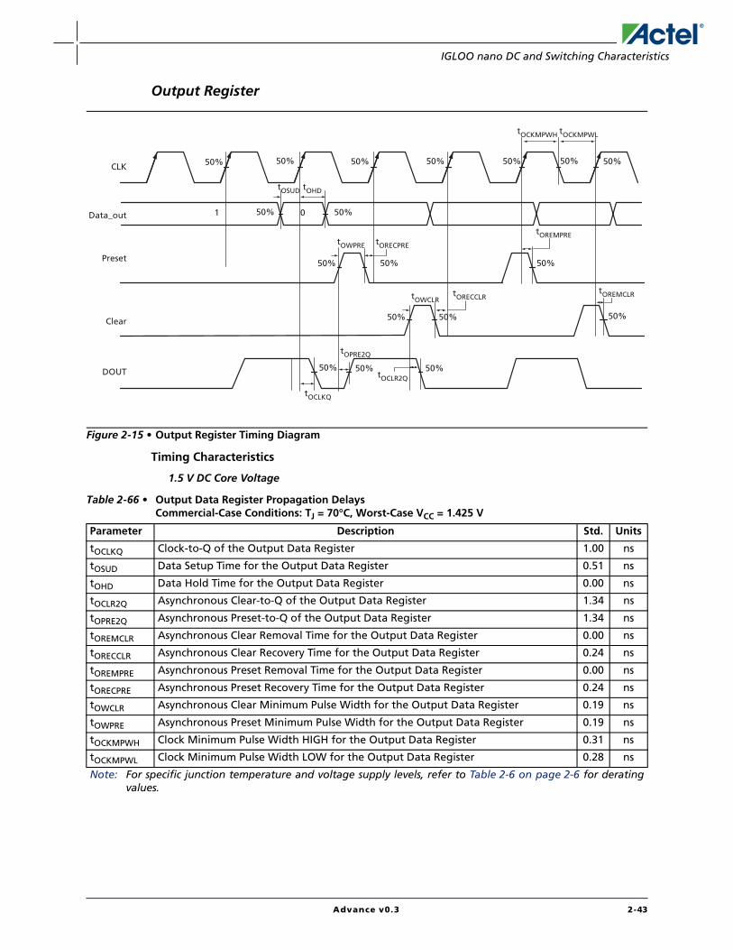
IGLOO nano DC and Switching Characteristics
Output Register
Timing Characteristics
1.5 V DC Core Voltage
Figure 2-15 • Output Register Timing Diagram
Clear
DOUT
CLK
Data_out
Preset
50%
tOSUD tOHD
50% 50%
tOCLKQ
1 0
tORECPRE
tOREMPRE
tORECCLRtOREMCLRtOWCLR
tOWPRE
tOPRE2Q
tOCLR2Q
tOCKMPWH tOCKMPWL
50% 50%
50% 50% 50%
50% 50%
50% 50% 50% 50% 50% 50%
50%
50%
Table 2-66 • Output Data Register Propagation DelaysCommercial-Case Conditions: TJ = 70°C, Worst-Case VCC = 1.425 V
Parameter Description Std. Units
tOCLKQ Clock-to-Q of the Output Data Register 1.00 ns
tOSUD Data Setup Time for the Output Data Register 0.51 ns
tOHD Data Hold Time for the Output Data Register 0.00 ns
tOCLR2Q Asynchronous Clear-to-Q of the Output Data Register 1.34 ns
tOPRE2Q Asynchronous Preset-to-Q of the Output Data Register 1.34 ns
tOREMCLR Asynchronous Clear Removal Time for the Output Data Register 0.00 ns
tORECCLR Asynchronous Clear Recovery Time for the Output Data Register 0.24 ns
tOREMPRE Asynchronous Preset Removal Time for the Output Data Register 0.00 ns
tORECPRE Asynchronous Preset Recovery Time for the Output Data Register 0.24 ns
tOWCLR Asynchronous Clear Minimum Pulse Width for the Output Data Register 0.19 ns
tOWPRE Asynchronous Preset Minimum Pulse Width for the Output Data Register 0.19 ns
tOCKMPWH Clock Minimum Pulse Width HIGH for the Output Data Register 0.31 ns
tOCKMPWL Clock Minimum Pulse Width LOW for the Output Data Register 0.28 ns
Note: For specific junction temperature and voltage supply levels, refer to Table 2-6 on page 2-6 for deratingvalues.
Advance v0.3 2-43

IGLOO nano DC and Switching Characteristics
1.2 V DC Core Voltage
Table 2-67 • Output Data Register Propagation DelaysCommercial-Case Conditions: TJ = 70°C, Worst-Case VCC = 1.14 V
Parameter Description Std. Units
tOCLKQ Clock-to-Q of the Output Data Register 1.52 ns
tOSUD Data Setup Time for the Output Data Register 1.15 ns
tOHD Data Hold Time for the Output Data Register 0.00 ns
tOCLR2Q Asynchronous Clear-to-Q of the Output Data Register 1.96 ns
tOPRE2Q Asynchronous Preset-to-Q of the Output Data Register 1.96 ns
tOREMCLR Asynchronous Clear Removal Time for the Output Data Register 0.00 ns
tORECCLR Asynchronous Clear Recovery Time for the Output Data Register 0.24 ns
tOREMPRE Asynchronous Preset Removal Time for the Output Data Register 0.00 ns
tORECPRE Asynchronous Preset Recovery Time for the Output Data Register 0.24 ns
tOWCLR Asynchronous Clear Minimum Pulse Width for the Output Data Register 0.19 ns
tOWPRE Asynchronous Preset Minimum Pulse Width for the Output Data Register 0.19 ns
tOCKMPWH Clock Minimum Pulse Width HIGH for the Output Data Register 0.31 ns
tOCKMPWL Clock Minimum Pulse Width LOW for the Output Data Register 0.28 ns
Note: For specific junction temperature and voltage supply levels, refer to Table 2-7 on page 2-7 for deratingvalues.
2-44 Advance v0.3

IGLOO nano DC and Switching Characteristics
Output Enable Register
Timing Characteristics
1.5 V DC Core Voltage
Figure 2-16 • Output Enable Register Timing Diagram
50%
Preset
Clear
EOUT
CLK
D_Enable
50%
tOESUD tOEHD
50% 50%
tOECLKQ
1 0
tOERECPREtOEREMPRE
tOERECCLR tOEREMCLRtOEWCLR
tOEWPRE
tOEPRE2QtOECLR2Q
tOECKMPWH tOECKMPWL
50% 50%
50% 50% 50%
50% 50%
50% 50% 50% 50% 50% 50%
50%
Table 2-68 • Output Enable Register Propagation DelaysCommercial-Case Conditions: TJ = 70°C, Worst-Case VCC = 1.425 V
Parameter Description Std. Units
tOECLKQ Clock-to-Q of the Output Enable Register 0.75 ns
tOESUD Data Setup Time for the Output Enable Register 0.51 ns
tOEHD Data Hold Time for the Output Enable Register 0.00 ns
tOECLR2Q Asynchronous Clear-to-Q of the Output Enable Register 1.13 ns
tOEPRE2Q Asynchronous Preset-to-Q of the Output Enable Register 1.13 ns
tOEREMCLR Asynchronous Clear Removal Time for the Output Enable Register 0.00 ns
tOERECCLR Asynchronous Clear Recovery Time for the Output Enable Register 0.24 ns
tOEREMPRE Asynchronous Preset Removal Time for the Output Enable Register 0.00 ns
tOERECPRE Asynchronous Preset Recovery Time for the Output Enable Register 0.24 ns
tOEWCLR Asynchronous Clear Minimum Pulse Width for the Output Enable Register 0.19 ns
tOEWPRE Asynchronous Preset Minimum Pulse Width for the Output Enable Register 0.19 ns
tOECKMPWH Clock Minimum Pulse Width HIGH for the Output Enable Register 0.31 ns
tOECKMPWL Clock Minimum Pulse Width LOW for the Output Enable Register 0.28 ns
Note: For specific junction temperature and voltage supply levels, refer to Table 2-6 on page 2-6 for deratingvalues.
Advance v0.3 2-45

IGLOO nano DC and Switching Characteristics
1.2 V DC Core Voltage
Table 2-69 • Output Enable Register Propagation DelaysCommercial-Case Conditions: TJ = 70°C, Worst-Case VCC = 1.14 V
Parameter Description Std. Units
tOECLKQ Clock-to-Q of the Output Enable Register 1.10 ns
tOESUD Data Setup Time for the Output Enable Register 1.15 ns
tOEHD Data Hold Time for the Output Enable Register 0.00 ns
tOECLR2Q Asynchronous Clear-to-Q of the Output Enable Register 1.65 ns
tOEPRE2Q Asynchronous Preset-to-Q of the Output Enable Register 1.65 ns
tOEREMCLR Asynchronous Clear Removal Time for the Output Enable Register 0.00 ns
tOERECCLR Asynchronous Clear Recovery Time for the Output Enable Register 0.24 ns
tOEREMPRE Asynchronous Preset Removal Time for the Output Enable Register 0.00 ns
tOERECPRE Asynchronous Preset Recovery Time for the Output Enable Register 0.24 ns
tOEWCLR Asynchronous Clear Minimum Pulse Width for the Output Enable Register 0.19 ns
tOEWPRE Asynchronous Preset Minimum Pulse Width for the Output Enable Register 0.19 ns
tOECKMPWH Clock Minimum Pulse Width HIGH for the Output Enable Register 0.31 ns
tOECKMPWL Clock Minimum Pulse Width LOW for the Output Enable Register 0.28 ns
Note: For specific junction temperature and voltage supply levels, refer to Table 2-7 on page 2-7 for deratingvalues.
2-46 Advance v0.3

IGLOO nano DC and Switching Characteristics
DDR Module Specifications
Input DDR Module
Figure 2-17 • Input DDR Timing Model
Table 2-70 • Parameter Definitions
Parameter Name Parameter Definition Measuring Nodes (from, to)
tDDRICLKQ1 Clock-to-Out Out_QR B, D
tDDRICLKQ2 Clock-to-Out Out_QF B, E
tDDRISUD Data Setup Time of DDR input A, B
tDDRIHD Data Hold Time of DDR input A, B
tDDRICLR2Q1 Clear-to-Out Out_QR C, D
tDDRICLR2Q2 Clear-to-Out Out_QF C, E
tDDRIREMCLR Clear Removal C, B
tDDRIRECCLR Clear Recovery C, B
Input DDR
Data
CLK
CLKBUF
INBUFOut_QF(to core)
FF2
FF1
INBUF
CLR
DDR_IN
E
A
B
C
D
Out_QR(to core)
Advance v0.3 2-47

IGLOO nano DC and Switching Characteristics
Timing Characteristics
1.5 V DC Core Voltage
Figure 2-18 • Input DDR Timing Diagram
tDDRICLR2Q2
tDDRIREMCLR
tDDRIRECCLR
tDDRICLR2Q1
1 2 3 4 5 6 7 8 9
CLK
Data
CLR
Out_QR
Out_QF
tDDRICLKQ1
2 4 6
3 5 7
tDDRIHDtDDRISUD
tDDRICLKQ2
Table 2-71 • Input DDR Propagation DelaysCommercial-Case Conditions: TJ = 70°C, Worst-Case VCC = 1.25 V
Parameter Description Std. Units
tDDRICLKQ1 Clock-to-Out Out_QR for Input DDR 0.48 ns
tDDRICLKQ2 Clock-to-Out Out_QF for Input DDR 0.65 ns
tDDRISUD1 Data Setup for Input DDR (negedge) 0.50 ns
tDDRISUD2 Data Setup for Input DDR (posedge) 0.40 ns
tDDRIHD1 Data Hold for Input DDR (negedge) 0.00 ns
tDDRIHD2 Data Hold for Input DDR (posedge) 0.00 ns
tDDRICLR2Q1 Asynchronous Clear-to-Out Out_QR for Input DDR 0.82 ns
tDDRICLR2Q2 Asynchronous Clear-to-Out Out_QF for Input DDR 0.98 ns
tDDRIREMCLR Asynchronous Clear Removal Time for Input DDR 0.00 ns
tDDRIRECCLR Asynchronous Clear Recovery Time for Input DDR 0.23 ns
tDDRIWCLR Asynchronous Clear Minimum Pulse Width for Input DDR 0.19 ns
tDDRICKMPWH Clock Minimum Pulse Width HIGH for Input DDR 0.31 ns
tDDRICKMPWL Clock Minimum Pulse Width LOW for Input DDR 0.28 ns
FDDRIMAX Maximum Frequency for Input DDR TBD MHz
Note: For specific junction temperature and voltage supply levels, refer to Table 2-7 on page 2-7 for deratingvalues.
2-48 Advance v0.3

IGLOO nano DC and Switching Characteristics
1.2 V DC Core Voltage
Table 2-72 • Input DDR Propagation DelaysCommercial-Case Conditions: TJ = 70°C, Worst-Case VCC = 1.14 V
Parameter Description Std. Units
tDDRICLKQ1 Clock-to-Out Out_QR for Input DDR 0.76 ns
tDDRICLKQ2 Clock-to-Out Out_QF for Input DDR 0.94 ns
tDDRISUD1 Data Setup for Input DDR (negedge) 0.93 ns
tDDRISUD2 Data Setup for Input DDR (posedge) 0.84 ns
tDDRIHD1 Data Hold for Input DDR (negedge) 0.00 ns
tDDRIHD2 Data Hold for Input DDR (posedge) 0.00 ns
tDDRICLR2Q1 Asynchronous Clear-to-Out Out_QR for Input DDR 1.23 ns
tDDRICLR2Q2 Asynchronous Clear-to-Out Out_QF for Input DDR 1.42 ns
tDDRIREMCLR Asynchronous Clear Removal Time for Input DDR 0.00 ns
tDDRIRECCLR Asynchronous Clear Recovery Time for Input DDR 0.24 ns
tDDRIWCLR Asynchronous Clear Minimum Pulse Width for Input DDR 0.19 ns
tDDRICKMPWH Clock Minimum Pulse Width HIGH for Input DDR 0.31 ns
tDDRICKMPWL Clock Minimum Pulse Width LOW for Input DDR 0.28 ns
FDDRIMAX Maximum Frequency for Input DDR TBD MHz
Note: For specific junction temperature and voltage supply levels, refer to Table 2-7 on page 2-7 for deratingvalues.
Advance v0.3 2-49

IGLOO nano DC and Switching Characteristics
Output DDR Module
Figure 2-19 • Output DDR Timing Model
Table 2-73 • Parameter Definitions
Parameter Name Parameter Definition Measuring Nodes (from, to)
tDDROCLKQ Clock-to-Out B, E
tDDROCLR2Q Asynchronous Clear-to-Out C, E
tDDROREMCLR Clear Removal C, B
tDDRORECCLR Clear Recovery C, B
tDDROSUD1 Data Setup Data_F A, B
tDDROSUD2 Data Setup Data_R D, B
tDDROHD1 Data Hold Data_F A, B
tDDROHD2 Data Hold Data_R D, B
Data_F(from core)
CLK
CLKBUF
Out
FF2
INBUFCLR
DDR_OUT
Output DDR
FF1
0
1
XX
X
X
X
X
X
X
A
B
D
EC
C
B
OUTBUFData_R(from core)
2-50 Advance v0.3

IGLOO nano DC and Switching Characteristics
Timing Characteristics
1.5 V DC Core Voltage
Figure 2-20 • Output DDR Timing Diagram
116
1
7
2
8
3
9 10
4 5
2 8 3 9
tDDROREMCLR
tDDROHD1tDDROREMCLR
tDDROHD2tDDROSUD2
tDDROCLKQ
tDDRORECCLR
CLK
Data_R
Data_F
CLR
Out
tDDROCLR2Q
7 104
Table 2-74 • Output DDR Propagation DelaysCommercial-Case Conditions: TJ = 70°C, Worst-Case VCC = 1.425 V
Parameter Description Std. Units
tDDROCLKQ Clock-to-Out of DDR for Output DDR 1.07 ns
tDDROSUD1 Data_F Data Setup for Output DDR 0.67 ns
tDDROSUD2 Data_R Data Setup for Output DDR 0.67 ns
tDDROHD1 Data_F Data Hold for Output DDR 0.00 ns
tDDROHD2 Data_R Data Hold for Output DDR 0.00 ns
tDDROCLR2Q Asynchronous Clear-to-Out for Output DDR 1.38 ns
tDDROREMCLR Asynchronous Clear Removal Time for Output DDR 0.00 ns
tDDRORECCLR Asynchronous Clear Recovery Time for Output DDR 0.23 ns
tDDROWCLR1 Asynchronous Clear Minimum Pulse Width for Output DDR 0.19 ns
tDDROCKMPWH Clock Minimum Pulse Width HIGH for the Output DDR 0.31 ns
tDDROCKMPWL Clock Minimum Pulse Width LOW for the Output DDR 0.28 ns
FDDOMAX Maximum Frequency for the Output DDR TBD MHz
Note: For specific junction temperature and voltage supply levels, refer to Table 2-6 on page 2-6 for deratingvalues.
Advance v0.3 2-51
IGLOO nano DC and Switching Characteristics
1.2 V DC Core Voltage
Table 2-75 • Output DDR Propagation DelaysCommercial-Case Conditions: TJ = 70°C, Worst-Case VCC = 1.14 V
Parameter Description Std. Units
tDDROCLKQ Clock-to-Out of DDR for Output DDR 1.60 ns
tDDROSUD1 Data_F Data Setup for Output DDR 1.09 ns
tDDROSUD2 Data_R Data Setup for Output DDR 1.16 ns
tDDROHD1 Data_F Data Hold for Output DDR 0.00 ns
tDDROHD2 Data_R Data Hold for Output DDR 0.00 ns
tDDROCLR2Q Asynchronous Clear-to-Out for Output DDR 1.99 ns
tDDROREMCLR Asynchronous Clear Removal Time for Output DDR 0.00 ns
tDDRORECCLR Asynchronous Clear Recovery Time for Output DDR 0.24 ns
tDDROWCLR1 Asynchronous Clear Minimum Pulse Width for Output DDR 0.19 ns
tDDROCKMPWH Clock Minimum Pulse Width HIGH for the Output DDR 0.31 ns
tDDROCKMPWL Clock Minimum Pulse Width LOW for the Output DDR 0.28 ns
FDDOMAX Maximum Frequency for the Output DDR TBD MHz
Note: For specific junction temperature and voltage supply levels, refer to Table 2-7 on page 2-7 for deratingvalues.
2-52 Advance v0.3

IGLOO nano DC and Switching Characteristics
VersaTile Characteristics
VersaTile Specifications as a Combinatorial ModuleThe IGLOO nano library offers all combinations of LUT-3 combinatorial functions. In this section,timing characteristics are presented for a sample of the library. For more details, refer to theFusion, IGLOO/e, and ProASIC3/ E Macro Library Guide.
Figure 2-21 • Sample of Combinatorial Cells
MAJ3A
C
B Y MUX2B
0
1
A
S
Y
A Y
B
B
AXOR2 Y
NOR2B
AY
B
AYOR2
INV
AYAND2
B
AY
NAND3BA
C
XOR3 YBA
C
NAND2
Advance v0.3 2-53

IGLOO nano DC and Switching Characteristics
Figure 2-22 • Timing Model and Waveforms
NetA
Y
B
Length = 1 VersaTile
NetA
Y
B
Length = 1 VersaTile
NetA
Y
B
Length = 1 VersaTile
NetA
Y
B
Length = 1 VersaTile
NAND2 or AnyCombinatorial
Logic
NAND2 or AnyCombinatorial
Logic
NAND2 or AnyCombinatorial
Logic
NAND2 or AnyCombinatorial
Logic
tPD = MAX(tPD(RR), tPD(RF),tPD(FF), tPD(FR)) where edges are applicable for a particularcombinatorial cell
Fanout = 4
tPD
tPD
tPD
50%
VCC
VCC
VCC
50%
GNDA, B, C50% 50%
50%
(RR)
(RF)GND
OUT
OUT
GND
50%
(FF)
(FR)
tPD
tPD
2-54 Advance v0.3

IGLOO nano DC and Switching Characteristics
Timing Characteristics1.5 V DC Core Voltage
1.2 V DC Core Voltage
Table 2-76 • Combinatorial Cell Propagation DelaysCommercial-Case Conditions: TJ = 70°C, Worst-Case VCC = 1.425 V
Combinatorial Cell Equation Parameter Std. Units
INV Y = !A tPD 0.76 ns
AND2 Y = A · B tPD 0.87 ns
NAND2 Y = !(A · B) tPD 0.91 ns
OR2 Y = A + B tPD 0.90 ns
NOR2 Y = !(A + B) tPD 0.94 ns
XOR2 Y = A ⊕ B tPD 1.39 ns
MAJ3 Y = MAJ(A, B, C) tPD 1.44 ns
XOR3 Y = A ⊕ B ⊕ C tPD 1.60 ns
MUX2 Y = A !S + B S tPD 1.17 ns
AND3 Y = A · B · C tPD 1.18 ns
Note: For specific junction temperature and voltage supply levels, refer to Table 2-6 on page 2-6 for deratingvalues.
Table 2-77 • Combinatorial Cell Propagation DelaysCommercial-Case Conditions: TJ = 70°C, Worst-Case VCC = 1.14 V
Combinatorial Cell Equation Parameter Std. Units
INV Y = !A tPD 1.33 ns
AND2 Y = A · B tPD 1.48 ns
NAND2 Y = !(A · B) tPD 1.58 ns
OR2 Y = A + B tPD 1.53 ns
NOR2 Y = !(A + B) tPD 1.63 ns
XOR2 Y = A ⊕ B tPD 2.34 ns
MAJ3 Y = MAJ(A, B, C) tPD 2.59 ns
XOR3 Y = A ⊕ B ⊕ C tPD 2.74 ns
MUX2 Y = A !S + B S tPD 2.03 ns
AND3 Y = A · B · C tPD 2.11 ns
Note: For specific junction temperature and voltage supply levels, refer to Table 2-7 on page 2-7 for deratingvalues.
Advance v0.3 2-55

IGLOO nano DC and Switching Characteristics
VersaTile Specifications as a Sequential ModuleThe IGLOO nano library offers a wide variety of sequential cells, including flip-flops and latches.Each has a data input and optional enable, clear, or preset. In this section, timing characteristics arepresented for a representative sample from the library. For more details, refer to the Fusion,IGLOO/e, and ProASIC3/E Macro Library Guide.
Figure 2-23 • Sample of Sequential Cells
D Q
DFN1
Data
CLK
Out
D Q
DFN1C1
Data
CLK
Out
CLR
D Q
DFI1E1P1
Data
CLK
Out
En
PRE
D Q
DFN1E1
Data
CLK
Out
En
2-56 Advance v0.3

IGLOO nano DC and Switching Characteristics
Timing Characteristics1.5 V DC Core Voltage
Figure 2-24 • Timing Model and Waveforms
PRE
CLR
Out
CLK
Data
EN
tSUE
50%
50%
tSUD
tHD
50% 50%
tCLKQ
0
tHE
tRECPRE tREMPRE
tRECCLR tREMCLRtWCLR
tWPRE
tPRE2QtCLR2Q
tCKMPWHtCKMPWL
50% 50%
50% 50% 50%
50% 50%
50% 50% 50% 50% 50% 50%
50%
50%
Table 2-78 • Register DelaysCommercial-Case Conditions: TJ = 70°C, Worst-Case VCC = 1.425 V
Parameter Description Std. Units
tCLKQ Clock-to-Q of the Core Register 0.89 ns
tSUD Data Setup Time for the Core Register 0.81 ns
tHD Data Hold Time for the Core Register 0.00 ns
tSUE Enable Setup Time for the Core Register 0.73 ns
tHE Enable Hold Time for the Core Register 0.00 ns
tCLR2Q Asynchronous Clear-to-Q of the Core Register 0.60 ns
tPRE2Q Asynchronous Preset-to-Q of the Core Register 0.62 ns
tREMCLR Asynchronous Clear Removal Time for the Core Register 0.00 ns
tRECCLR Asynchronous Clear Recovery Time for the Core Register 0.24 ns
tREMPRE Asynchronous Preset Removal Time for the Core Register 0.00 ns
tRECPRE Asynchronous Preset Recovery Time for the Core Register 0.23 ns
tWCLR Asynchronous Clear Minimum Pulse Width for the Core Register 0.30 ns
tWPRE Asynchronous Preset Minimum Pulse Width for the Core Register 0.30 ns
tCKMPWH Clock Minimum Pulse Width HIGH for the Core Register 0.56 ns
tCKMPWL Clock Minimum Pulse Width LOW for the Core Register 0.56 ns
Note: For specific junction temperature and voltage supply levels, refer to Table 2-6 on page 2-6 for deratingvalues.
Advance v0.3 2-57

IGLOO nano DC and Switching Characteristics
1.2 V DC Core Voltage
Table 2-79 • Register DelaysCommercial-Case Conditions: TJ = 70°C, Worst-Case VCC = 1.14 V
Parameter Description Std. Units
tCLKQ Clock-to-Q of the Core Register 1.61 ns
tSUD Data Setup Time for the Core Register 1.17 ns
tHD Data Hold Time for the Core Register 0.00 ns
tSUE Enable Setup Time for the Core Register 1.29 ns
tHE Enable Hold Time for the Core Register 0.00 ns
tCLR2Q Asynchronous Clear-to-Q of the Core Register 0.87 ns
tPRE2Q Asynchronous Preset-to-Q of the Core Register 0.89 ns
tREMCLR Asynchronous Clear Removal Time for the Core Register 0.00 ns
tRECCLR Asynchronous Clear Recovery Time for the Core Register 0.24 ns
tREMPRE Asynchronous Preset Removal Time for the Core Register 0.00 ns
tRECPRE Asynchronous Preset Recovery Time for the Core Register 0.24 ns
tWCLR Asynchronous Clear Minimum Pulse Width for the Core Register 0.46 ns
tWPRE Asynchronous Preset Minimum Pulse Width for the Core Register 0.46 ns
tCKMPWH Clock Minimum Pulse Width HIGH for the Core Register 0.95 ns
tCKMPWL Clock Minimum Pulse Width LOW for the Core Register 0.95 ns
Note: For specific junction temperature and voltage supply levels, refer to Table 2-7 on page 2-7 for deratingvalues.
2-58 Advance v0.3

IGLOO nano DC and Switching Characteristics
Global Resource Characteristics
AGLN125 Clock Tree TopologyClock delays are device-specific. Figure 2-25 is an example of a global tree used for clock routing.The global tree presented in Figure 2-25 is driven by a CCC located on the west side of theAGLN125 device. It is used to drive all D-flip-flops in the device.
Figure 2-25 • Example of Global Tree Use in an AGLN125 Device for Clock Routing
CentralGlobal Rib
VersaTileRows
Global Spine
CCC
Advance v0.3 2-59

IGLOO nano DC and Switching Characteristics
Global Tree Timing CharacteristicsGlobal clock delays include the central rib delay, the spine delay, and the row delay. Delays do notinclude I/O input buffer clock delays, as these are I/O standard–dependent, and the clock may bedriven and conditioned internally by the CCC module. For more details on clock conditioningcapabilities, refer to the "Clock Conditioning Circuits" section on page 2-66. Table 2-80 toTable 2-88 on page 2-64 present minimum and maximum global clock delays within each device.Minimum and maximum delays are measured with minimum and maximum loading.
Timing Characteristics
1.5 V DC Core Voltage
Table 2-80 • AGLN010 Global ResourceCommercial-Case Conditions: TJ = 70°C, VCC = 1.425 V
Parameter Description
Std.
UnitsMin.1 Max.2
tRCKL Input LOW Delay for Global Clock 1.08 1.36 ns
tRCKH Input HIGH Delay for Global Clock 1.09 1.44 ns
tRCKMPWH Minimum Pulse Width HIGH for Global Clock ns
tRCKMPWL Minimum Pulse Width LOW for Global Clock ns
tRCKSW Maximum Skew for Global Clock 0.35 ns
FRMAX Maximum Frequency for Global Clock MHz
Notes:
1. Value reflects minimum load. The delay is measured from the CCC output to the clock pin of a sequentialelement, located in a lightly loaded row (single element is connected to the global net).
2. Value reflects maximum load. The delay is measured on the clock pin of the farthest sequential element,located in a fully loaded row (all available flip-flops are connected to the global net in the row).
3. For specific junction temperature and voltage supply levels, refer to Table 2-6 on page 2-6 for deratingvalues.
Table 2-81 • AGLN015 Global ResourceCommercial-Case Conditions: TJ = 70°C, VCC = 1.425 V
Parameter Description
Std.
UnitsMin.1 Max.2
tRCKL Input LOW Delay for Global Clock 1.15 1.49 ns
tRCKH Input HIGH Delay for Global Clock 1.16 1.59 ns
tRCKMPWH Minimum Pulse Width HIGH for Global Clock ns
tRCKMPWL Minimum Pulse Width LOW for Global Clock ns
tRCKSW Maximum Skew for Global Clock 0.42 ns
FRMAX Maximum Frequency for Global Clock MHz
Notes:
1. Value reflects minimum load. The delay is measured from the CCC output to the clock pin of a sequentialelement, located in a lightly loaded row (single element is connected to the global net).
2. Value reflects maximum load. The delay is measured on the clock pin of the farthest sequential element,located in a fully loaded row (all available flip-flops are connected to the global net in the row).
3. For specific junction temperature and voltage supply levels, refer to Table 2-6 on page 2-6 for deratingvalues.
2-60 Advance v0.3

IGLOO nano DC and Switching Characteristics
Table 2-82 • AGLN020 Global ResourceCommercial-Case Conditions: TJ = 70°C, VCC = 1.425 V
Parameter Description
Std.
UnitsMin.1 Max.2
tRCKL Input LOW Delay for Global Clock 1.15 1.49 ns
tRCKH Input HIGH Delay for Global Clock 1.16 1.59 ns
tRCKMPWH Minimum Pulse Width HIGH for Global Clock ns
tRCKMPWL Minimum Pulse Width LOW for Global Clock ns
tRCKSW Maximum Skew for Global Clock 0.42 ns
FRMAX Maximum Frequency for Global Clock MHz
Notes:
1. Value reflects minimum load. The delay is measured from the CCC output to the clock pin of a sequentialelement, located in a lightly loaded row (single element is connected to the global net).
2. Value reflects maximum load. The delay is measured on the clock pin of the farthest sequential element,located in a fully loaded row (all available flip-flops are connected to the global net in the row).
3. For specific junction temperature and voltage supply levels, refer to Table 2-6 on page 2-6 for deratingvalues.
Table 2-83 • AGLN060 Global ResourceCommercial-Case Conditions: TJ = 70°C, VCC = 1.425 V
Parameter Description
Std.
UnitsMin.1 Max.2
tRCKL Input LOW Delay for Global Clock 1.32 1.67 ns
tRCKH Input HIGH Delay for Global Clock 1.34 1.76 ns
tRCKMPWH Minimum Pulse Width HIGH for Global Clock ns
tRCKMPWL Minimum Pulse Width LOW for Global Clock ns
tRCKSW Maximum Skew for Global Clock 0.42 ns
FRMAX Maximum Frequency for Global Clock MHz
Notes:
1. Value reflects minimum load. The delay is measured from the CCC output to the clock pin of a sequentialelement, located in a lightly loaded row (single element is connected to the global net).
2. Value reflects maximum load. The delay is measured on the clock pin of the farthest sequential element,located in a fully loaded row (all available flip-flops are connected to the global net in the row).
3. For specific junction temperature and voltage supply levels, refer to Table 2-6 on page 2-6 for deratingvalues.
Advance v0.3 2-61

IGLOO nano DC and Switching Characteristics
Table 2-84 • AGLN125 Global ResourceCommercial-Case Conditions: TJ = 70°C, VCC = 1.425 V
Parameter Description
Std.
UnitsMin.1 Max.2
tRCKL Input LOW Delay for Global Clock 1.36 1.71 ns
tRCKH Input HIGH Delay for Global Clock 1.39 1.82 ns
tRCKMPWH Minimum Pulse Width HIGH for Global Clock ns
tRCKMPWL Minimum Pulse Width LOW for Global Clock ns
tRCKSW Maximum Skew for Global Clock 0.43 ns
FRMAX Maximum Frequency for Global Clock MHz
Notes:
1. Value reflects minimum load. The delay is measured from the CCC output to the clock pin of a sequentialelement, located in a lightly loaded row (single element is connected to the global net).
2. Value reflects maximum load. The delay is measured on the clock pin of the farthest sequential element,located in a fully loaded row (all available flip-flops are connected to the global net in the row).
3. For specific junction temperature and voltage supply levels, refer to Table 2-6 on page 2-6 for deratingvalues.
Table 2-85 • AGLN250 Global ResourceCommercial-Case Conditions: TJ = 70°C, VCC = 1.425 V
Parameter Description
Std.
UnitsMin.1 Max.2
tRCKL Input LOW Delay for Global Clock 1.39 1.73 ns
tRCKH Input HIGH Delay for Global Clock 1.41 1.84 ns
tRCKMPWH Minimum Pulse Width HIGH for Global Clock ns
tRCKMPWL Minimum Pulse Width LOW for Global Clock ns
tRCKSW Maximum Skew for Global Clock 0.43 ns
FRMAX Maximum Frequency for Global Clock MHz
Notes:
1. Value reflects minimum load. The delay is measured from the CCC output to the clock pin of a sequentialelement, located in a lightly loaded row (single element is connected to the global net).
2. Value reflects maximum load. The delay is measured on the clock pin of the farthest sequential element,located in a fully loaded row (all available flip-flops are connected to the global net in the row).
3. For specific junction temperature and voltage supply levels, refer to Table 2-6 on page 2-6 for deratingvalues.
2-62 Advance v0.3

IGLOO nano DC and Switching Characteristics
1.2 V DC Core Voltage
Table 2-86 • AGLN010 Global ResourceCommercial-Case Conditions: TJ = 70°C, VCC = 1.14 V
Parameter Description
Std.
UnitsMin.1 Max.2
tRCKL Input LOW Delay for Global Clock TBD TBD ns
tRCKH Input HIGH Delay for Global Clock TBD TBD ns
tRCKMPWH Minimum Pulse Width HIGH for Global Clock ns
tRCKMPWL Minimum Pulse Width LOW for Global Clock ns
tRCKSW Maximum Skew for Global Clock TBD ns
FRMAX Maximum Frequency for Global Clock MHz
Notes:
1. Value reflects minimum load. The delay is measured from the CCC output to the clock pin of a sequentialelement, located in a lightly loaded row (single element is connected to the global net).
2. Value reflects maximum load. The delay is measured on the clock pin of the farthest sequential element,located in a fully loaded row (all available flip-flops are connected to the global net in the row).
3. For specific junction temperature and voltage supply levels, refer to Table 2-7 on page 2-7 for deratingvalues.
Table 2-87 • AGLN015 Global ResourceCommercial-Case Conditions: TJ = 70°C, VCC = 1.14 V
Parameter Description
Std.
UnitsMin.1 Max.2
tRCKL Input LOW Delay for Global Clock TBD TBD ns
tRCKH Input HIGH Delay for Global Clock TBD TBD ns
tRCKMPWH Minimum Pulse Width HIGH for Global Clock ns
tRCKMPWL Minimum Pulse Width LOW for Global Clock ns
tRCKSW Maximum Skew for Global Clock TBD ns
FRMAX Maximum Frequency for Global Clock MHz
Notes:
1. Value reflects minimum load. The delay is measured from the CCC output to the clock pin of a sequentialelement, located in a lightly loaded row (single element is connected to the global net).
2. Value reflects maximum load. The delay is measured on the clock pin of the farthest sequential element,located in a fully loaded row (all available flip-flops are connected to the global net in the row).
3. For specific junction temperature and voltage supply levels, refer to Table 2-7 on page 2-7 for deratingvalues.
Advance v0.3 2-63

IGLOO nano DC and Switching Characteristics
Table 2-88 • AGLN020 Global ResourceCommercial-Case Conditions: TJ = 70°C, VCC = 1.14 V
Parameter Description
Std.
UnitsMin.1 Max.2
tRCKL Input LOW Delay for Global Clock TBD TBD ns
tRCKH Input HIGH Delay for Global Clock TBD TBD ns
tRCKMPWH Minimum Pulse Width HIGH for Global Clock ns
tRCKMPWL Minimum Pulse Width LOW for Global Clock ns
tRCKSW Maximum Skew for Global Clock TBD ns
FRMAX Maximum Frequency for Global Clock MHz
Notes:
1. Value reflects minimum load. The delay is measured from the CCC output to the clock pin of a sequentialelement, located in a lightly loaded row (single element is connected to the global net).
2. Value reflects maximum load. The delay is measured on the clock pin of the farthest sequential element,located in a fully loaded row (all available flip-flops are connected to the global net in the row).
3. For specific junction temperature and voltage supply levels, refer to Table 2-7 on page 2-7 for deratingvalues.
Table 2-89 • AGLN060 Global ResourceCommercial-Case Conditions: TJ = 70°C, VCC = 1.14 V
Parameter Description
Std.
UnitsMin.1 Max.2
tRCKL Input LOW Delay for Global Clock 2.02 2.49 ns
tRCKH Input HIGH Delay for Global Clock 2.09 2.72 ns
tRCKMPWH Minimum Pulse Width HIGH for Global Clock ns
tRCKMPWL Minimum Pulse Width LOW for Global Clock ns
tRCKSW Maximum Skew for Global Clock 0.63 ns
FRMAX Maximum Frequency for Global Clock MHz
Notes:
1. Value reflects minimum load. The delay is measured from the CCC output to the clock pin of a sequentialelement, located in a lightly loaded row (single element is connected to the global net).
2. Value reflects maximum load. The delay is measured on the clock pin of the farthest sequential element,located in a fully loaded row (all available flip-flops are connected to the global net in the row).
3. For specific junction temperature and voltage supply levels, refer to Table 2-7 on page 2-7 for deratingvalues.
2-64 Advance v0.3

IGLOO nano DC and Switching Characteristics
Table 2-90 • AGLN125 Global ResourceCommercial-Case Conditions: TJ = 70°C, VCC = 1.14 V
Parameter Description
Std.
UnitsMin.1 Max.2
tRCKL Input LOW Delay for Global Clock 2.08 2.54 ns
tRCKH Input HIGH Delay for Global Clock 2.15 2.77 ns
tRCKMPWH Minimum Pulse Width HIGH for Global Clock ns
tRCKMPWL Minimum Pulse Width LOW for Global Clock ns
tRCKSW Maximum Skew for Global Clock 0.62 ns
FRMAX Maximum Frequency for Global Clock MHz
Notes:
1. Value reflects minimum load. The delay is measured from the CCC output to the clock pin of a sequentialelement, located in a lightly loaded row (single element is connected to the global net).
2. Value reflects maximum load. The delay is measured on the clock pin of the farthest sequential element,located in a fully loaded row (all available flip-flops are connected to the global net in the row).
3. For specific junction temperature and voltage supply levels, refer to Table 2-7 on page 2-7 for deratingvalues.
Table 2-91 • AGLN250 Global ResourceCommercial-Case Conditions: TJ = 70°C, VCC = 1.14 V
Parameter Description
Std.
UnitsMin.1 Max.2
tRCKL Input LOW Delay for Global Clock 2.11 2.57 ns
tRCKH Input HIGH Delay for Global Clock 2.19 2.81 ns
tRCKMPWH Minimum Pulse Width HIGH for Global Clock ns
tRCKMPWL Minimum Pulse Width LOW for Global Clock ns
tRCKSW Maximum Skew for Global Clock 0.62 ns
FRMAX Maximum Frequency for Global Clock MHz
Notes:
1. Value reflects minimum load. The delay is measured from the CCC output to the clock pin of a sequentialelement, located in a lightly loaded row (single element is connected to the global net).
2. Value reflects maximum load. The delay is measured on the clock pin of the farthest sequential element,located in a fully loaded row (all available flip-flops are connected to the global net in the row).
3. For specific junction temperature and voltage supply levels, refer to Table 2-7 on page 2-7 for deratingvalues.
Advance v0.3 2-65

IGLOO nano DC and Switching Characteristics
Clock Conditioning CircuitsCCC Electrical SpecificationsTiming Characteristics
Table 2-92 • IGLOO nano CCC/PLL SpecificationFor IGLOO nano V2 or V5 devices, 1.5 V DC Core Supply Voltage
Parameter Min. Typ. Max. Units
Clock Conditioning Circuitry Input Frequency fIN_CCC 1.5 250 MHz
Clock Conditioning Circuitry Output Frequency fOUT_CCC 0.75 250 MHz
Delay Increments in Programmable Delay Blocks 1, 2 360 ps
Number of Programmable Values in Each Programmable Delay Block 32
Serial Clock (SCLK) for Dynamic PLL 5 100
Input Cycle-to-Cycle Jitter (peak magnitude) 1 ns
CCC Output Peak-to-Peak Period Jitter FCCC_OUT Max Peak-to-Peak Period Jitter
1 Global Network
Used
External FB Used
3 Global Networks
Used
0.75 MHz to 24 MHz 0.50% 0.75% 0.70%
24 MHz to 100 MHz 1.00% 1.50% 1.20%
100 MHz to 250 MHz 2.50% 3.75% 2.75%
Acquisition Time
LockControl = 0 300 µs
LockControl = 1 6.0 ms
Tracking Jitter
LockControl = 0 2.5 ns
LockControl = 1 1.5 ns
Output Duty Cycle 48.5 51.5 %
Delay Range in Block: Programmable Delay 1 1, 2 1.25 15.65 ns
Delay Range in Block: Programmable Delay 2 1, 2 0.025 15.65 ns
Delay Range in Block: Fixed Delay 1, 2 3.5 ns
Notes:
1. This delay is a function of voltage and temperature. See Table 2-6 on page 2-6 and Table 2-7 on page 2-7for deratings.
2. TJ = 25°C, VCC = 1.5 V
3. The AGLN010, AGLN015, and AGLN020 devices do not support PLL.
4. Tracking jitter is defined as the variation in clock edge position of PLL outputs with reference to the PLLinput clock edge. Tracking jitter does not measure the variation in PLL output period, which is covered bythe period jitter parameter.
5. Maximum value obtained for a STD speed grade device in Worst-Case Commercial conditions. For specificjunction temperature and voltage supply levels, refer to Table 2-6 on page 2-6 and Table 2-7 on page 2-7for derating values.
2-66 Advance v0.3
IGLOO nano DC and Switching Characteristics
Table 2-93 • IGLOO nano CCC/PLL SpecificationFor IGLOO nano V2 Devices, 1.2 V DC Core Supply Voltage
Parameter Min. Typ. Max. Units
Clock Conditioning Circuitry Input Frequency fIN_CCC 1.5 160 MHz
Clock Conditioning Circuitry Output Frequency fOUT_CCC 0.75 160 MHz
Delay Increments in Programmable Delay Blocks 1, 2 580 ps
Number of Programmable Values in Each Programmable Delay Block 32
Serial Clock (SCLK) for Dynamic PLL 5 60 MHz
Input Cycle-to-Cycle Jitter (peak magnitude) 0.25 ns
CCC Output Peak-to-Peak Period Jitter FCCC_OUT Max Peak-to-Peak Period Jitter
1 Global Network
Used
External FB Used
3 Global Networks
Used
0.75 MHz to 24 MHz 0.50% 0.75% 0.70%
24 MHz to 100 MHz 1.00% 1.50% 1.20%
100 MHz to 160 MHz 2.50% 3.75% 2.75%
Acquisition Time
LockControl = 0 300 µs
LockControl = 1 6.0 ms
Tracking Jitter
LockControl = 0 4 ns
LockControl = 1 3 ns
Output Duty Cycle 48.5 51.5 %
Delay Range in Block: Programmable Delay 1 1, 2 2.3 20.86 ns
Delay Range in Block: Programmable Delay 2 1, 2, 0.025 20.86 ns
Delay Range in Block: Fixed Delay 1, 2 5.7 ns
Notes:
1. This delay is a function of voltage and temperature. See Table 2-6 on page 2-6 and Table 2-7 on page 2-7for deratings.
2. TJ = 25°C, VCC = 1.2 V
3. The AGLN010, AGLN015, and AGLN020 devices do not support PLLs.
4. Tracking jitter is defined as the variation in clock edge position of PLL outputs with reference to PLL inputclock edge. Tracking jitter does not measure the variation in PLL output period, which is covered by periodjitter parameter.
5. Maximum value obtained for a STD speed grade device in Worst-Case Commercial conditions. For specificjunction temperature and voltage supply levels, refer to Table 2-6 on page 2-6 and Table 2-7 on page 2-7for derating values.
Advance v0.3 2-67

IGLOO nano DC and Switching Characteristics
Note: Peak-to-peak jitter measurements are defined by Tpeak-to-peak = Tperiod_max – Tperiod_min.Figure 2-26 • Peak-to-Peak Jitter Definition
Tperiod_max Tperiod_min
Output Signal
2-68 Advance v0.3

IGLOO nano DC and Switching Characteristics
Embedded SRAM and FIFO Characteristics
SRAM
Figure 2-27 • RAM Models
ADDRA11 DOUTA8DOUTA7
DOUTA0
DOUTB8DOUTB7
DOUTB0
ADDRA10
ADDRA0DINA8DINA7
DINA0
WIDTHA1WIDTHA0PIPEAWMODEABLKAWENACLKA
ADDRB11ADDRB10
ADDRB0
DINB8DINB7
DINB0
WIDTHB1WIDTHB0PIPEBWMODEBBLKBWENBCLKB
RAM4K9
RADDR8 RD17RADDR7 RD16
RADDR0 RD0
WD17WD16
WD0
WW1WW0
RW1RW0
PIPE
RENRCLK
RAM512X18
WADDR8WADDR7
WADDR0
WENWCLK
RESETRESET
Advance v0.3 2-69

IGLOO nano DC and Switching Characteristics
Timing Waveforms
Figure 2-28 • RAM Read for Pass-Through Output
Figure 2-29 • RAM Read for Pipelined Output
CLK
ADD
BLK_B
WEN_B
DO
A0 A1 A2
D0 D1 D2
tCYC
tCKH tCKL
tAS tAH
tBKS
tENS tENH
tDOH1
tBKH
Dn
tCKQ1
CLK
ADD
BLK_B
WEN_B
DO
A0 A1 A2
D0 D1
tCYCtCKH tCKL
tAS
tAH
tBKS
tENS tENH
tDOH2
tCKQ2
tBKH
Dn
2-70 Advance v0.3

IGLOO nano DC and Switching Characteristics
Figure 2-30 • RAM Write, Output Retained (WMODE = 0)
Figure 2-31 • RAM Write, Output as Write Data (WMODE = 1)
tCYC
tCKH tCKL
A0 A1 A2
DI0 DI1
tAS tAH
tBKS
tENS tENH
tDS tDH
CLK
BLK_B
WEN_B
ADD
DI
DnDO
tBKH
D2
tCYC
tCKH tCKL
A0 A1 A2
DI0 DI1
tAS tAH
tBKS
tENS
tDS tDH
CLK
BLK_B
WEN_B
ADD
DI
tBKH
DO(pass-through)
DI1Dn DI0
DO(pipelined)
DI0 DI1Dn
DI2
Advance v0.3 2-71

IGLOO nano DC and Switching Characteristics
Figure 2-32 • RAM Reset
CLK
RESET_B
DO Dn
tCYC
tCKH tCKL
tRSTBQ
Dm
2-72 Advance v0.3

IGLOO nano DC and Switching Characteristics
Timing Characteristics1.5 V DC Core Voltage
Table 2-94 • RAM4K9Commercial-Case Conditions: TJ = 70°C, Worst-Case VCC = 1.425 V
Parameter Description Std. Units
tAS Address setup time 0.83 ns
tAH Address hold time 0.16 ns
tENS REN_B, WEN_B setup time 0.81 ns
tENH REN_B, WEN_B hold time 0.16 ns
tBKS BLK_B setup time 1.65 ns
tBKH BLK_B hold time 0.16 ns
tDS Input data (DI) setup time 0.71 ns
tDH Input data (DI) hold time 0.36 ns
tCKQ1 Clock HIGH to new data valid on DO (output retained, WMODE = 0) 3.53 ns
Clock HIGH to new data valid on DO (flow-through, WMODE = 1) 3.06 ns
tCKQ2 Clock HIGH to new data valid on DO (pipelined) 1.81 ns
tC2CWWL Address collision clk-to-clk delay for reliable write after write on same address;applicable to closing edge
0.23 ns
tC2CRWH Address collision clk-to-clk delay for reliable read access after write on same address;applicable to opening edge
0.35 ns
tC2CWRH Address collision clk-to-clk delay for reliable write access after read on same address;applicable to opening edge
0.41 ns
tRSTBQ RESET_B LOW to data out LOW on DO (flow-through) 2.06 ns
RESET_B LOW to data out LOW on DO (pipelined) 2.06 ns
tREMRSTB RESET_B removal 0.61 ns
tRECRSTB RESET_B recovery 3.21 ns
tMPWRSTB RESET_B minimum pulse width 0.68 ns
tCYC Clock cycle time 6.24 ns
FMAX Maximum frequency 160 MHz
Note: For specific junction temperature and voltage supply levels, refer to Table 2-6 on page 2-6 for deratingvalues.
Advance v0.3 2-73

IGLOO nano DC and Switching Characteristics
Table 2-95 • RAM512X18Commercial-Case Conditions: TJ = 70°C, Worst-Case VCC = 1.425 V
Parameter Description Std. Units
tAS Address setup time 0.83 ns
tAH Address hold time 0.16 ns
tENS REN_B, WEN_B setup time 0.73 ns
tENH REN_B, WEN_B hold time 0.08 ns
tDS Input data (DI) setup time 0.71 ns
tDH Input data (DI) hold time 0.36 ns
tCKQ1 Clock HIGH to new data valid on DO (output retained, WMODE = 0) 4.21 ns
tCKQ2 Clock HIGH to new data valid on DO (pipelined) 1.71 ns
tC2CRWH Address collision clk-to-clk delay for reliable read access after write on same address;applicable to opening edge
0.35 ns
tC2CWRH Address collision clk-to-clk delay for reliable write access after read on same address;applicable to opening edge
0.42 ns
tRSTBQ RESET_B LOW to data out LOW on DO (flow-through) 2.06 ns
RESET_B LOW to data out LOW on DO (pipelined) 2.06 ns
tREMRSTB RESET_B removal 0.61 ns
tRECRSTB RESET_B recovery 3.21 ns
tMPWRSTB RESET_B minimum pulse width 0.68 ns
tCYC Clock cycle time 6.24 ns
FMAX Maximum frequency 160 MHz
Note: For specific junction temperature and voltage supply levels, refer to Table 2-6 on page 2-6 for deratingvalues.
2-74 Advance v0.3
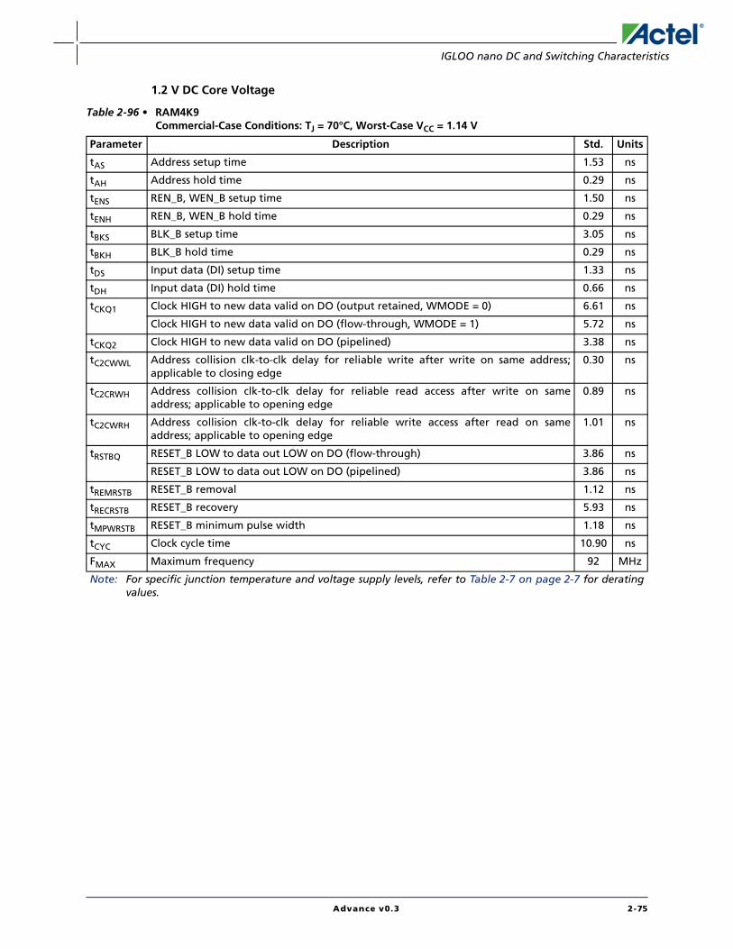
IGLOO nano DC and Switching Characteristics
1.2 V DC Core Voltage
Table 2-96 • RAM4K9Commercial-Case Conditions: TJ = 70°C, Worst-Case VCC = 1.14 V
Parameter Description Std. Units
tAS Address setup time 1.53 ns
tAH Address hold time 0.29 ns
tENS REN_B, WEN_B setup time 1.50 ns
tENH REN_B, WEN_B hold time 0.29 ns
tBKS BLK_B setup time 3.05 ns
tBKH BLK_B hold time 0.29 ns
tDS Input data (DI) setup time 1.33 ns
tDH Input data (DI) hold time 0.66 ns
tCKQ1 Clock HIGH to new data valid on DO (output retained, WMODE = 0) 6.61 ns
Clock HIGH to new data valid on DO (flow-through, WMODE = 1) 5.72 ns
tCKQ2 Clock HIGH to new data valid on DO (pipelined) 3.38 ns
tC2CWWL Address collision clk-to-clk delay for reliable write after write on same address;applicable to closing edge
0.30 ns
tC2CRWH Address collision clk-to-clk delay for reliable read access after write on sameaddress; applicable to opening edge
0.89 ns
tC2CWRH Address collision clk-to-clk delay for reliable write access after read on sameaddress; applicable to opening edge
1.01 ns
tRSTBQ RESET_B LOW to data out LOW on DO (flow-through) 3.86 ns
RESET_B LOW to data out LOW on DO (pipelined) 3.86 ns
tREMRSTB RESET_B removal 1.12 ns
tRECRSTB RESET_B recovery 5.93 ns
tMPWRSTB RESET_B minimum pulse width 1.18 ns
tCYC Clock cycle time 10.90 ns
FMAX Maximum frequency 92 MHz
Note: For specific junction temperature and voltage supply levels, refer to Table 2-7 on page 2-7 for deratingvalues.
Advance v0.3 2-75

IGLOO nano DC and Switching Characteristics
Table 2-97 • RAM512X18Commercial-Case Conditions: TJ = 70°C, Worst-Case VCC = 1.14 V
Parameter Description Std. Units
tAS Address setup time 1.53 ns
tAH Address hold time 0.29 ns
tENS REN_B, WEN_B setup time 1.36 ns
tENH REN_B, WEN_B hold time 0.15 ns
tDS Input data (DI) setup time 1.33 ns
tDH Input data (DI) hold time 0.66 ns
tCKQ1 Clock HIGH to new data valid on DO (output retained, WMODE = 0) 7.88 ns
tCKQ2 Clock HIGH to new data valid on DO (pipelined) 3.20 ns
tC2CRWH Address collision clk-to-clk delay for reliable read access after write on same address;applicable to opening edge
0.87 ns
tC2CWRH Address collision clk-to-clk delay for reliable write access after read on same address;applicable to opening edge
1.04 ns
tRSTBQ RESET_B LOW to data out LOW on DO (flow through) 3.86 ns
RESET_B LOW to data out LOW on DO (pipelined) 3.86 ns
tREMRSTB RESET_B removal 1.12 ns
tRECRSTB RESET_B recovery 5.93 ns
tMPWRSTB RESET_B minimum pulse width 1.18 ns
tCYC Clock cycle time 10.90 ns
FMAX Maximum frequency 92 MHz
Note: For specific junction temperature and voltage supply levels, refer to Table 2-7 on page 2-7 for deratingvalues.
2-76 Advance v0.3

IGLOO nano DC and Switching Characteristics
FIFO
Figure 2-33 • FIFO Model
FIFO4K18
RW2 RD17RW1 RD16RW0 WW2 WW1WW0 RD0ESTOPFSTOP FULL
AFULLEMPTY
AFVAL11
AEMPTY
AFVAL10
AFVAL0
AEVAL11AEVAL10
AEVAL0
RENRBLKRCLK
WENWBLKWCLK
RPIPE
WD17WD16
WD0
RESET
Advance v0.3 2-77
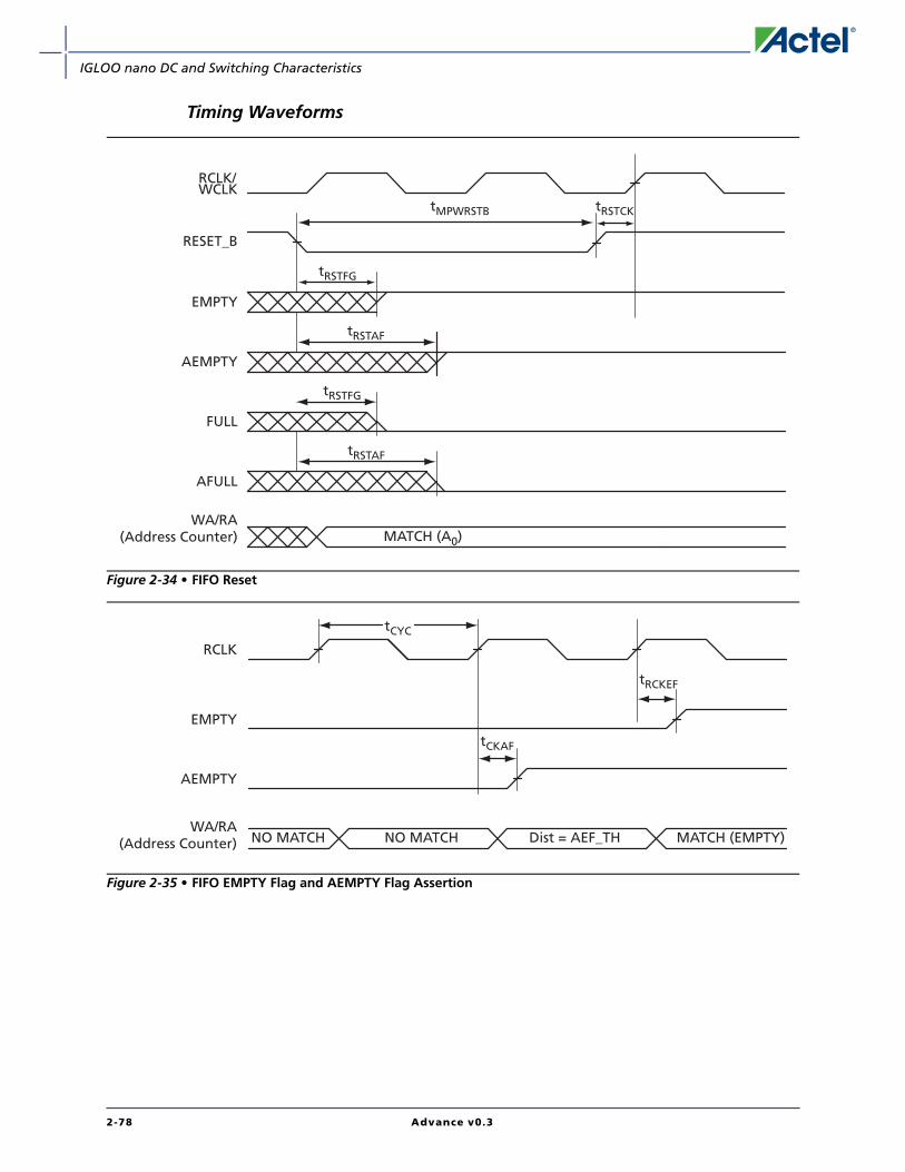
IGLOO nano DC and Switching Characteristics
Timing Waveforms
Figure 2-34 • FIFO Reset
Figure 2-35 • FIFO EMPTY Flag and AEMPTY Flag Assertion
MATCH (A0)
tMPWRSTB
tRSTFG
tRSTCK
tRSTAF
RCLK/WCLK
RESET_B
EMPTY
AEMPTY
WA/RA(Address Counter)
tRSTFG
tRSTAF
FULL
AFULL
RCLK
NO MATCH NO MATCH Dist = AEF_TH MATCH (EMPTY)
tCKAF
tRCKEF
EMPTY
AEMPTY
tCYC
WA/RA(Address Counter)
2-78 Advance v0.3

IGLOO nano DC and Switching Characteristics
Figure 2-36 • FIFO FULL Flag and AFULL Flag Assertion
Figure 2-37 • FIFO EMPTY Flag and AEMPTY Flag Deassertion
Figure 2-38 • FIFO FULL Flag and AFULL Flag Deassertion
NO MATCH NO MATCH Dist = AFF_TH MATCH (FULL)
tCKAF
tWCKFF
tCYC
WCLK
FULL
AFULL
WA/RA(Address Counter)
WCLK
WA/RA(Address Counter)
MATCH(EMPTY) NO MATCH NO MATCH NO MATCH Dist = AEF_TH + 1NO MATCH
RCLK
EMPTY
1st RisingEdge
After 1stWrite
2nd RisingEdge
After 1stWrite
tRCKEF
tCKAF
AEMPTY
Dist = AFF_TH – 1MATCH (FULL) NO MATCH NO MATCH NO MATCH NO MATCH
tWCKF
tCKAF
1st RisingEdge
After 1stRead
1st RisingEdge
After 2ndRead
RCLK
WA/RA(Address Counter)
WCLK
FULL
AFULL
Advance v0.3 2-79

IGLOO nano DC and Switching Characteristics
Timing Characteristics1.5 V DC Core Voltage
Table 2-98 • FIFOWorst Commercial-Case Conditions: TJ = 70°C, VCC = 1.425 V
Parameter Description Std. Units
tENS REN_B, WEN_B Setup Time 1.99 ns
tENH REN_B, WEN_B Hold Time 0.16 ns
tBKS BLK_B Setup Time 0.30 ns
tBKH BLK_B Hold Time 0.00 ns
tDS Input Data (DI) Setup Time 0.76 ns
tDH Input Data (DI) Hold Time 0.25 ns
tCKQ1 Clock HIGH to New Data Valid on DO (flow-through) 3.33 ns
tCKQ2 Clock HIGH to New Data Valid on DO (pipelined) 1.80 ns
tRCKEF RCLK HIGH to Empty Flag Valid 3.53 ns
tWCKFF WCLK HIGH to Full Flag Valid 3.35 ns
tCKAF Clock HIGH to Almost Empty/Full Flag Valid 12.85 ns
tRSTFG RESET_B LOW to Empty/Full Flag Valid 3.48 ns
tRSTAF RESET_B LOW to Almost Empty/Full Flag Valid 12.72 ns
tRSTBQ RESET_B LOW to Data Out LOW on DO (flow-through) 2.02 ns
RESET_B LOW to Data Out LOW on DO (pipelined) 2.02 ns
tREMRSTB RESET_B Removal 0.61 ns
tRECRSTB RESET_B Recovery 3.21 ns
tMPWRSTB RESET_B Minimum Pulse Width 0.68 ns
tCYC Clock Cycle Time 6.24 ns
FMAX Maximum Frequency for FIFO 160 MHz
Note: For specific junction temperature and voltage supply levels, refer to Table 2-6 on page 2-6 for deratingvalues.
2-80 Advance v0.3

IGLOO nano DC and Switching Characteristics
1.2 V DC Core Voltage
Table 2-99 • FIFOWorst Commercial-Case Conditions: TJ = 70°C, VCC = 1.14 V
Parameter Description Std. Units
tENS REN_B, WEN_B Setup Time 4.13 ns
tENH REN_B, WEN_B Hold Time 0.31 ns
tBKS BLK_B Setup Time 0.30 ns
tBKH BLK_B Hold Time 0.00 ns
tDS Input Data (DI) Setup Time 1.56 ns
tDH Input Data (DI) Hold Time 0.49 ns
tCKQ1 Clock HIGH to New Data Valid on DO (flow-through) 6.80 ns
tCKQ2 Clock HIGH to New Data Valid on DO (pipelined) 3.62 ns
tRCKEF RCLK HIGH to Empty Flag Valid 7.23 ns
tWCKFF WCLK HIGH to Full Flag Valid 6.85 ns
tCKAF Clock HIGH to Almost Empty/Full Flag Valid 26.61 ns
tRSTFG RESET_B LOW to Empty/Full Flag Valid 7.12 ns
tRSTAF RESET_B LOW to Almost Empty/Full Flag Valid 26.33 ns
tRSTBQ RESET_B LOW to Data Out LOW on DO (flow-through) 4.09 ns
RESET_B LOW to Data Out LOW on DO (pipelined) 4.09 ns
tREMRSTB RESET_B Removal 1.23 ns
tRECRSTB RESET_B Recovery 6.58 ns
tMPWRSTB RESET_B Minimum Pulse Width 1.18 ns
tCYC Clock Cycle Time 10.90 ns
FMAX Maximum Frequency for FIFO 92 MHz
Note: For specific junction temperature and voltage supply levels, refer to Table 2-7 on page 2-7 for deratingvalues.
Advance v0.3 2-81

IGLOO nano DC and Switching Characteristics
Embedded FlashROM Characteristics
Timing Characteristics1.5 V DC Core Voltage
1.2 V DC Core Voltage
Figure 2-39 • Timing Diagram
A0 A1
tSU
tHOLD
tSU
tHOLD
tSU
tHOLD
tCKQ2 tCKQ2 tCKQ2
CLK
Address
Data D0 D0 D1
Table 2-100 • Embedded FlashROM Access TimeWorst Commercial-Case Conditions: TJ = 70°C, VCC = 1.425 V
Parameter Description Std. Units
tSU Address Setup Time 0.57 ns
tHOLD Address Hold Time 0.00 ns
tCK2Q Clock to Out 20.90 ns
FMAX Maximum Clock Frequency 15 MHz
Table 2-101 • Embedded FlashROM Access TimeWorst Commercial-Case Conditions: TJ = 70°C, VCC = 1.14 V
Parameter Description Std. Units
tSU Address Setup Time 0.59 ns
tHOLD Address Hold Time 0.00 ns
tCK2Q Clock to Out 35.74 ns
FMAX Maximum Clock Frequency 10 MHz
2-82 Advance v0.3

IGLOO nano DC and Switching Characteristics
JTAG 1532 CharacteristicsJTAG timing delays do not include JTAG I/Os. To obtain complete JTAG timing, add I/O buffer delaysto the corresponding standard selected; refer to the I/O timing characteristics in the "User I/OCharacteristics" section on page 2-15 for more details.
Timing Characteristics1.5 V DC Core Voltage
1.2 V DC Core Voltage
Table 2-102 • JTAG 1532Commercial-Case Conditions: TJ = 70°C, Worst-Case VCC = 1.425 V
Parameter Description Std. Units
tDISU Test Data Input Setup Time 1.00 ns
tDIHD Test Data Input Hold Time 2.00 ns
tTMSSU Test Mode Select Setup Time 1.00 ns
tTMDHD Test Mode Select Hold Time 2.00 ns
tTCK2Q Clock to Q (data out) 8.00 ns
tRSTB2Q Reset to Q (data out) 25.00 ns
FTCKMAX TCK Maximum Frequency 15 MHz
tTRSTREM ResetB Removal Time 0.58 ns
tTRSTREC ResetB Recovery Time 0.00 ns
tTRSTMPW ResetB Minimum Pulse TBD ns
Note: For specific junction temperature and voltage supply levels, refer to Table 2-6 on page 2-6 for deratingvalues.
Table 2-103 • JTAG 1532Commercial-Case Conditions: TJ = 70°C, Worst-Case VCC = 1.14 V
Parameter Description Std. Units
tDISU Test Data Input Setup Time 1.50 ns
tDIHD Test Data Input Hold Time 3.00 ns
tTMSSU Test Mode Select Setup Time 1.50 ns
tTMDHD Test Mode Select Hold Time 3.00 ns
tTCK2Q Clock to Q (data out) 11.00 ns
tRSTB2Q Reset to Q (data out) 30.00 ns
FTCKMAX TCK Maximum Frequency 9.00 MHz
tTRSTREM ResetB Removal Time 1.18 ns
tTRSTREC ResetB Recovery Time 0.00 ns
tTRSTMPW ResetB Minimum Pulse TBD ns
Note: For specific junction temperature and voltage supply levels, refer to Table 2-6 on page 2-6 for deratingvalues.
Advance v0.3 2-83
IGLOO nano DC and Switching Characteristics
Part Number and Revision DatePart Number 51700110-002-2Revised April 2009
List of ChangesThe following table lists critical changes that were made in the current version of the chapter.
Previous Version Changes in Current Version (Advance v0.3) Page
Advance v0.2(November 2008)
Reference to the –F speed grade was removed from this document, since it is nolonger offered for IGLOO nano devices.
2-1
Advance v0.1(October 2008)
The table notes and references were revised in Table 2-2 · RecommendedOperating Conditions 1. VMV was included with VCCI and a table note was addedstating, "VMV pins must be connected to the corresponding VCCI pins. See PinDescriptions for further information." Please review carefully.
2-2
VJTAG was added to the list in the table note for Table 2-8 · Quiescent SupplyCurrent (IDD) Characteristics, IGLOO nano Flash*Freeze Mode*. Values wereadded for AGLN010, AGLN015, and AGLN030 for 1.5 V.
2-7
VCCI was removed from the list in the table note for Table 2-9 · Quiescent SupplyCurrent (IDD) Characteristics, IGLOO nano Sleep Mode (VCC = 0 V)*.
2-7
Values for ICCA current were updated for AGLN010, AGLN015, and AGLN030 inTable 2-11 · Quiescent Supply Current (IDD), No IGLOO nano Flash*Freeze Mode1.
2-8
Values for PAC1 and PAC2 were added to Table 2-14 · Different ComponentsContributing to Dynamic Power Consumption in IGLOO nano Devices andTable 2-16 · Different Components Contributing to Dynamic Power Consumptionin IGLOO nano Devices.
2-10, 2-11
Table notes regarding wide range support were added to Table 2-20 · Summaryof Maximum and Minimum DC Input and Output Levels.
2-19
1.2 V LVCMOS wide range values were added to Table 2-21 · Summary ofMaximum and Minimum DC Input Levels and Table 2-22 · Summary of ACMeasuring Points.
2-19, 2-20
The following table note was added to Table 2-24 · Summary of I/O TimingCharacteristics—Software Default Settings and Table 2-25 · Summary of I/OTiming Characteristics—Software Default Settings: "All LVCMOS 3.3 V softwaremacros support LVCMOS 3.3 V wide range, as specified in the JESD8-Bspecification."
2-21
3.3 V LVCMOS Wide Range and 1.2 V Wide Range were added to Table 2-27 · I/OOutput Buffer Maximum Resistances 1 andTable 2-29 · I/O Short CurrentsIOSH/IOSL.
2-22, 2-23
2-84 Advance v0.3

IGLOO nano DC and Switching Characteristics
Actel Safety Critical, Life Support, and High-Reliability Applications Policy
The Actel products described in this advance status datasheet may not have completed Actel’squalification process. Actel may amend or enhance products during the product introduction andqualification process, resulting in changes in device functionality or performance. It is theresponsibility of each customer to ensure the fitness of any Actel product (but especially a newproduct) for a particular purpose, including appropriateness for safety-critical, life-support, andother high-reliability applications. Consult Actel’s Terms and Conditions for specific liabilityexclusions relating to life-support applications. A reliability report covering all of Actel’s products isavailable on the Actel website at http://www.actel.com/documents/ORT_Report.pdf. Actel alsooffers a variety of enhanced qualification and lot acceptance screening procedures. Contact yourlocal Actel sales office for additional reliability information.
Advance v0.3 2-85


IGLOO nano Packaging
3 – Package Pin Assignments
36-Pin UC
NoteFor Package Manufacturing and Environmental information, visit the Resource Center athttp://www.actel.com/products/solutions/package/docs.aspx.
Note: This is the bottom view of the package.
6 5 4 3 2 1
A
B
C
D
E
F
Pin 1 Pad Corner
Advance v0.7 3-1

Package Pin Assignments
36-Pin UC
Pin Number AGLN010 Function
A1 IO21RSB1
A2 IO18RSB1
A3 IO13RSB1
A4 GDC0/IO00RSB0
A5 IO06RSB0
A6 GDA0/IO04RSB0
B1 GEC0/IO37RSB1
B2 IO20RSB1
B3 IO15RSB1
B4 IO09RSB0
B5 IO08RSB0
B6 IO07RSB0
C1 IO22RSB1
C2 GEA0/IO34RSB1
C3 GND
C4 GND
C5 VCCIB0
C6 IO02RSB0
D1 IO33RSB1
D2 VCCIB1
D3 VCC
D4 VCC
D5 IO10RSB0
D6 IO11RSB0
E1 IO32RSB1
E2 FF/IO31RSB1
E3 TCK
E4 VPUMP
E5 TRST
E6 VJTAG
F1 IO29RSB1
F2 IO25RSB1
F3 IO23RSB1
F4 TDI
F5 TMS
F6 TDO
3-2 Advance v0.7

IGLOO nano Packaging
81-Pin UC
NoteFor Package Manufacturing and Environmental information, visit the Resource Center athttp://www.actel.com/products/solutions/package/docs.aspx.
Note: This is the bottom view of the package.
123456789
ABCDEFGHJ
A1 Ball Pad Corner
Advance v0.7 3-3

Package Pin Assignments
81-Pin UC
Pin Number AGLN020 Function
A1 IO64RSB2
A2 IO54RSB2
A3 IO57RSB2
A4 IO36RSB1
A5 IO32RSB1
A6 IO24RSB1
A7 IO20RSB1
A8 IO04RSB0
A9 IO08RSB0
B1 IO59RSB2
B2 IO55RSB2
B3 IO62RSB2
B4 IO34RSB1
B5 IO28RSB1
B6 IO22RSB1
B7 IO18RSB1
B8 IO00RSB0
B9 IO03RSB0
C1 IO51RSB2
C2 IO50RSB2
C3 NC
C4 NC
C5 NC
C6 NC
C7 NC
C8 IO10RSB0
C9 IO07RSB0
D1 IO49RSB2
D2 IO44RSB2
D3 NC
D4 VCC
D5 VCCIB2
D6 GND
D7 NC
D8 IO13RSB0
D9 IO12RSB0
E1 GEC0/IO48RSB2
E2 GEA0/IO47RSB2
E3 NC
E4 VCCIB1
E5 VCC
E6 VCCIB0
E7 NC
E8 GDA0/IO15RSB0
E9 GDC0/IO14RSB0
F1 IO46RSB2
F2 IO45RSB2
F3 NC
F4 GND
F5 VCCIB1
F6 NC
F7 NC
F8 IO16RSB0
F9 IO17RSB0
G1 IO43RSB2
G2 IO42RSB2
G3 IO41RSB2
G4 IO31RSB1
G5 NC
G6 IO21RSB1
G7 NC
G8 VJTAG
G9 TRST
H1 IO40RSB2
H2 FF/IO39RSB1
H3 IO35RSB1
H4 IO29RSB1
H5 IO26RSB1
H6 IO25RSB1
H7 IO19RSB1
H8 TDI
H9 TDO
81-Pin UC
Pin Number AGLN020 Function
J1 IO38RSB1
J2 IO37RSB1
J3 IO33RSB1
J4 IO30RSB1
J5 IO27RSB1
J6 IO23RSB1
J7 TCK
J8 TMS
J9 VPUMP
81-Pin UC
Pin Number AGLN020 Function
3-4 Advance v0.7

IGLOO nano Packaging
81-Pin UC
Pin Number AGLN030 Function
A1 IO00RSB0
A2 IO02RSB0
A3 IO06RSB0
A4 IO11RSB0
A5 IO16RSB0
A6 IO19RSB0
A7 IO22RSB0
A8 IO24RSB0
A9 IO26RSB0
B1 IO81RSB1
B2 IO04RSB0
B3 IO10RSB0
B4 IO13RSB0
B5 IO15RSB0
B6 IO20RSB0
B7 IO21RSB0
B8 IO28RSB0
B9 IO25RSB0
C1 IO79RSB1
C2 IO80RSB1
C3 IO08RSB0
C4 IO12RSB0
C5 IO17RSB0
C6 IO14RSB0
C7 IO18RSB0
C8 IO29RSB0
C9 IO27RSB0
D1 IO74RSB1
D2 IO76RSB1
D3 IO77RSB1
D4 VCC
D5 VCCIB0
D6 GND
D7 IO23RSB0
D8 IO31RSB0
D9 IO30RSB0
E1 GEB0/IO71RSB1
E2 GEA0/IO72RSB1
E3 GEC0/IO73RSB1
E4 VCCIB1
E5 VCC
E6 VCCIB0
E7 GDC0/IO32RSB0
E8 GDA0/IO33RSB0
E9 GDB0/IO34RSB0
F1 IO68RSB1
F2 IO67RSB1
F3 IO64RSB1
F4 GND
F5 VCCIB1
F6 IO47RSB1
F7 IO36RSB0
F8 IO38RSB0
F9 IO40RSB0
G1 IO65RSB1
G2 IO66RSB1
G3 IO57RSB1
G4 IO53RSB1
G5 IO49RSB1
G6 IO45RSB1
G7 IO46RSB1
G8 VJTAG
G9 TRST
H1 IO62RSB1
H2 FF/IO60RSB1
H3 IO58RSB1
H4 IO54RSB1
H5 IO48RSB1
H6 IO43RSB1
H7 IO42RSB1
H8 TDI
H9 TDO
81-Pin UC
Pin Number AGLN030 Function
J1 IO63RSB1
J2 IO61RSB1
J3 IO59RSB1
J4 IO56RSB1
J5 IO52RSB1
J6 IO44RSB1
J7 TCK
J8 TMS
J9 VPUMP
81-Pin UC
Pin Number AGLN030 Function
Advance v0.7 3-5

Package Pin Assignments
81-Pin CS
NoteFor Package Manufacturing and Environmental information, visit the Resource Center athttp://www.actel.com/products/solutions/package/docs.aspx.
Pin AssignmentsPin assignments for the 81-Pin CS package will be published in a future version of this document.
Note: This is the bottom view of the package.
123456789
ABCDEFGHJ
A1 Ball Pad Corner
3-6 Advance v0.7

IGLOO nano Packaging
81-Pin CS
Pin Number AGLN020 Function
A1 IO64RSB2
A2 IO54RSB2
A3 IO57RSB2
A4 IO36RSB1
A5 IO32RSB1
A6 IO24RSB1
A7 IO20RSB1
A8 IO04RSB0
A9 IO08RSB0
B1 IO59RSB2
B2 IO55RSB2
B3 IO62RSB2
B4 IO34RSB1
B5 IO28RSB1
B6 IO22RSB1
B7 IO18RSB1
B8 IO00RSB0
B9 IO03RSB0
C1 IO51RSB2
C2 IO50RSB2
C3 NC
C4 NC
C5 NC
C6 NC
C7 NC
C8 IO10RSB0
C9 IO07RSB0
D1 IO49RSB2
D2 IO44RSB2
D3 NC
D4 VCC
D5 VCCIB2
D6 GND
D7 NC
D8 IO13RSB0
D9 IO12RSB0
E1 GEC0/IO48RSB2
E2 GEA0/IO47RSB2
E3 NC
E4 VCCIB1
E5 VCC
E6 VCCIB0
E7 NC
E8 GDA0/IO15RSB0
E9 GDC0/IO14RSB0
F1 IO46RSB2
F2 IO45RSB2
F3 NC
F4 GND
F5 VCCIB1
F6 NC
F7 NC
F8 IO16RSB0
F9 IO17RSB0
G1 IO43RSB2
G2 IO42RSB2
G3 IO41RSB2
G4 IO31RSB1
G5 NC
G6 IO21RSB1
G7 NC
G8 VJTAG
G9 TRST
H1 IO40RSB2
H2 FF/IO39RSB1
H3 IO35RSB1
H4 IO29RSB1
H5 IO26RSB1
H6 IO25RSB1
H7 IO19RSB1
H8 TDI
H9 TDO
81-Pin CS
Pin Number AGLN020 Function
J1 IO38RSB1
J2 IO37RSB1
J3 IO33RSB1
J4 IO30RSB1
J5 IO27RSB1
J6 IO23RSB1
J7 TCK
J8 TMS
J9 VPUMP
81-Pin CS
Pin Number AGLN020 Function
Advance v0.7 3-7

Package Pin Assignments
81-Pin CS
Pin Number AGNL030 Function
A1 IO00RSB0
A2 IO02RSB0
A3 IO06RSB0
A4 IO11RSB0
A5 IO16RSB0
A6 IO19RSB0
A7 IO22RSB0
A8 IO24RSB0
A9 IO26RSB0
B1 IO81RSB1
B2 IO04RSB0
B3 IO10RSB0
B4 IO13RSB0
B5 IO15RSB0
B6 IO20RSB0
B7 IO21RSB0
B8 IO28RSB0
B9 IO25RSB0
C1 IO79RSB1
C2 IO80RSB1
C3 IO08RSB0
C4 IO12RSB0
C5 IO17RSB0
C6 IO14RSB0
C7 IO18RSB0
C8 IO29RSB0
C9 IO27RSB0
D1 IO74RSB1
D2 IO76RSB1
D3 IO77RSB1
D4 VCC
D5 VCCIB0
D6 GND
D7 IO23RSB0
D8 IO31RSB0
D9 IO30RSB0
E1 GEB0/IO71RSB1
E2 GEA0/IO72RSB1
E3 GEC0/IO73RSB1
E4 VCCIB1
E5 VCC
E6 VCCIB0
E7 GDC0/IO32RSB0
E8 GDA0/IO33RSB0
E9 GDB0/IO34RSB0
F1 IO68RSB1
F2 IO67RSB1
F3 IO64RSB1
F4 GND
F5 VCCIB1
F6 IO47RSB1
F7 IO36RSB0
F8 IO38RSB0
F9 IO40RSB0
G1 IO65RSB1
G2 IO66RSB1
G3 IO57RSB1
G4 IO53RSB1
G5 IO49RSB1
G6 IO44RSB1
G7 IO46RSB1
G8 VJTAG
G9 TRST
H1 IO62RSB1
H2 FF/IO60RSB1
H3 IO58RSB1
H4 IO54RSB1
H5 IO48RSB1
H6 IO43RSB1
H7 IO42RSB1
H8 TDI
H9 TDO
81-Pin CS
Pin Number AGNL030 Function
J1 IO63RSB1
J2 IO61RSB1
J3 IO59RSB1
J4 IO56RSB1
J5 IO52RSB1
J6 IO45RSB1
J7 TCK
J8 TMS
J9 VPUMP
81-Pin CS
Pin Number AGNL030 Function
3-8 Advance v0.7

IGLOO nano Packaging
81-Pin CS
Pin Number AGLN060 Function
A1 GAA0/IO02RSB0
A2 GAA1/IO03RSB0
A3 GAC0/IO06RSB0
A4 IO09RSB0
A5 IO13RSB0
A6 IO18RSB0
A7 GBB0/IO21RSB0
A8 GBA1/IO24RSB0
A9 GBA2/IO25RSB0
B1 GAA2/IO95RSB1
B2 GAB0/IO04RSB0
B3 GAC1/IO07RSB0
B4 IO08RSB0
B5 IO15RSB0
B6 GBC0/IO19RSB0
B7 GBB1/IO22RSB0
B8 IO26RSB0
B9 GBB2/IO27RSB0
C1 GAB2/IO93RSB1
C2 IO94RSB1
C3 GND
C4 IO10RSB0
C5 IO17RSB0
C6 GND
C7 GBA0/IO23RSB0
C8 GBC2/IO29RSB0
C9 IO31RSB0
D1 GAC2/IO91RSB1
D2 IO92RSB1
D3 GFA2/IO80RSB1
D4 VCC
D5 VCCIB0
D6 GND
D7 GCC2/IO43RSB0
D8 GCC1/IO35RSB0
D9 GCC0/IO36RSB0
E1 GFB0/IO83RSB1
E2 GFB1/IO84RSB1
E3 GFA1/IO81RSB1
E4 VCCIB1
E5 VCC
E6 VCCIB0
E7 GCA1/IO39RSB0
E8 GCA0/IO40RSB0
E9 GCB2/IO42RSB0
F1 VCCPLF
F2 VCOMPLF
F3 GND
F4 GND
F5 VCCIB1
F6 GND
F7 GDA1/IO49RSB0
F8 GDC1/IO45RSB0
F9 GDC0/IO46RSB0
G1 GEA0/IO69RSB1
G2 GEC1/IO74RSB1
G3 GEB1/IO72RSB1
G4 IO63RSB1
G5 IO60RSB1
G6 IO54RSB1
G7 GDB2/IO52RSB1
G8 VJTAG
G9 TRST
H1 GEA1/IO70RSB1
H2 FF/GEB2/IO67RSB1
H3 IO65RSB1
H4 IO62RSB1
H5 IO59RSB1
H6 IO56RSB1
H7 GDA2/IO51RSB1
H8 TDI
H9 TDO
81-Pin CS
Pin Number AGLN060 Function
J1 GEA2/IO68RSB1
J2 GEC2/IO66RSB1
J3 IO64RSB1
J4 IO61RSB1
J5 IO58RSB1
J6 IO55RSB1
J7 TCK
J8 TMS
J9 VPUMP
81-Pin CS
Pin Number AGLN060 Function
Advance v0.7 3-9

Package Pin Assignments
81-Pin CS
Pin Number AGLN060Z Function
A1 GAA0/IO02RSB0
A2 GAA1/IO03RSB0
A3 GAC0/IO06RSB0
A4 IO09RSB0
A5 IO13RSB0
A6 IO18RSB0
A7 GBB0/IO21RSB0
A8 GBA1/IO24RSB0
A9 GBA2/IO25RSB0
B1 GAA2/IO95RSB1
B2 GAB0/IO04RSB0
B3 GAC1/IO07RSB0
B4 IO08RSB0
B5 IO15RSB0
B6 GBC0/IO19RSB0
B7 GBB1/IO22RSB0
B8 IO26RSB0
B9 GBB2/IO27RSB0
C1 GAB2/IO93RSB1
C2 IO94RSB1
C3 GND
C4 IO10RSB0
C5 IO17RSB0
C6 GND
C7 GBA0/IO23RSB0
C8 GBC2/IO29RSB0
C9 IO31RSB0
D1 GAC2/IO91RSB1
D2 IO92RSB1
D3 GFA2/IO80RSB1
D4 VCC
D5 VCCIB0
D6 GND
D7 GCC2/IO43RSB0
D8 GCC1/IO35RSB0
D9 GCC0/IO36RSB0
E1 GFB0/IO83RSB1
E2 GFB1/IO84RSB1
E3 GFA1/IO81RSB1
E4 VCCIB1
E5 VCC
E6 VCCIB0
E7 GCA1/IO39RSB0
E8 GCA0/IO40RSB0
E9 GCB2/IO42RSB0
F1 VCCPLF
F2 VCOMPLF
F3 GND
F4 GND
F5 VCCIB1
F6 GND
F7 GDA1/IO49RSB0
F8 GDC1/IO45RSB0
F9 GDC0/IO46RSB0
G1 GEA0/IO69RSB1
G2 GEC1/IO74RSB1
G3 GEB1/IO72RSB1
G4 IO63RSB1
G5 IO60RSB1
G6 IO54RSB1
G7 GDB2/IO52RSB1
G8 VJTAG
G9 TRST
H1 GEA1/IO70RSB1
H2 FF/GEB2/IO67RSB1
H3 IO65RSB1
H4 IO62RSB1
H5 IO59RSB1
H6 IO56RSB1
H7 GDA2/IO51RSB1
H8 TDI
H9 TDO
81-Pin CS
Pin Number AGLN060Z Function
J1 GEA2/IO68RSB1
J2 GEC2/IO66RSB1
J3 IO64RSB1
J4 IO61RSB1
J5 IO58RSB1
J6 IO55RSB1
J7 TCK
J8 TMS
J9 VPUMP
81-Pin CS
Pin Number AGLN060Z Function
3-10 Advance v0.7

IGLOO nano Packaging
81-Pin CS
Pin Number AGLN125Z Function
A1 GAA0/IO00RSB0
A2 GAA1/IO01RSB0
A3 GAC0/IO04RSB0
A4 IO13RSB0
A5 IO22RSB0
A6 IO32RSB0
A7 GBB0/IO37RSB0
A8 GBA1/IO40RSB0
A9 GBA2/IO41RSB0
B1 GAA2/IO132RSB1
B2 GAB0/IO02RSB0
B3 GAC1/IO05RSB0
B4 IO11RSB0
B5 IO25RSB0
B6 GBC0/IO35RSB0
B7 GBB1/IO38RSB0
B8 IO42RSB0
B9 GBB2/IO43RSB0
C1 GAB2/IO130RSB1
C2 IO131RSB1
C3 GND
C4 IO15RSB0
C5 IO28RSB0
C6 GND
C7 GBA0/IO39RSB0
C8 GBC2/IO45RSB0
C9 IO47RSB0
D1 GAC2/IO128RSB1
D2 IO129RSB1
D3 GFA2/IO117RSB1
D4 VCC
D5 VCCIB0
D6 GND
D7 GCC2/IO59RSB0
D8 GCC1/IO51RSB0
D9 GCC0/IO52RSB0
E1 GFB0/IO120RSB1
E2 GFB1/IO121RSB1
E3 GFA1/IO118RSB1
E4 VCCIB1
E5 VCC
E6 VCCIB0
E7 GCA0/IO56RSB0
E8 GCA1/IO55RSB0
E9 GCB2/IO58RSB0
F1 VCCPLF
F2 VCOMPLF
F3 GND
F4 GND
F5 VCCIB1
F6 GND
F7 GDA1/IO65RSB0
F8 GDC1/IO61RSB0
F9 GDC0/IO62RSB0
G1 GEA0/IO104RSB1
G2 GEC0/IO108RSB1
G3 GEB1/IO107RSB1
G4 IO96RSB1
G5 IO92RSB1
G6 IO72RSB1
G7 GDB2/IO68RSB1
G8 VJTAG
G9 TRST
H1 GEA1/IO105RSB1
H2 FF/GEB2/IO102RSB1
H3 IO99RSB1
H4 IO94RSB1
H5 IO91RSB1
H6 IO81RSB1
H7 GDA2/IO67RSB1
H8 TDI
H9 TDO
81-Pin CS
Pin Number AGLN125Z Function
J1 GEA2/IO103RSB1
J2 GEC2/IO101RSB1
J3 IO97RSB1
J4 IO93RSB1
J5 IO90RSB1
J6 IO78RSB1
J7 TCK
J8 TMS
J9 VPUMP
81-Pin CS
Pin Number AGLN125Z Function
Advance v0.7 3-11

Package Pin Assignments
81-Pin CS
Pin Number AGLN250 Function
A1 GAA0/IO00RSB0
A2 GAA1/IO01RSB0
A3 GAC0/IO04RSB0
A4 IO13RSB0
A5 IO21RSB0
A6 IO27RSB0
A7 GBB0/IO37RSB0
A8 GBA1/IO40RSB0
A9 GBA2/IO41PPB1
B1 GAA2/IO118UPB3
B2 GAB0/IO02RSB0
B3 GAC1/IO05RSB0
B4 IO11RSB0
B5 IO23RSB0
B6 GBC0/IO35RSB0
B7 GBB1/IO38RSB0
B8 IO41NPB1
B9 GBB2/IO42PSB1
C1 GAB2/IO117UPB3
C2 IO118VPB3
C3 GND
C4 IO15RSB0
C5 IO25RSB0
C6 GND
C7 GBA0/IO39RSB0
C8 GBC2/IO43PDB1
C9 IO43NDB1
D1 GAC2/IO116USB3
D2 IO117VPB3
D3 GFA2/IO107PSB3
D4 VCC
D5 VCCIB0
D6 GND
D7 IO52NPB1
D8 GCC1/IO48PDB1
D9 GCC0/IO48NDB1
E1 GFB0/IO109NDB3
E2 GFB1/IO109PDB3
E3 GFA1/IO108PSB3
E4 VCCIB3
E5 VCC
E6 VCCIB1
E7 GCA0/IO50NDB1
E8 GCA1/IO50PDB1
E9 GCB2/IO52PPB1
F1 VCCPLF
F2 VCOMPLF
F3 GND
F4 GND
F5 VCCIB2
F6 GND
F7 GDA1/IO60USB1
F8 GDC1/IO58UDB1
F9 GDC0/IO58VDB1
G1 GEA0/IO98NDB3
G2 GEC1/IO100PDB3
G3 GEC0/IO100NDB3
G4 IO91RSB2
G5 IO86RSB2
G6 IO71RSB2
G7 GDB2/IO62RSB2
G8 VJTAG
G9 TRST
H1 GEA1/IO98PDB3
H2 FF/GEB2/IO96RSB2
H3 IO93RSB2
H4 IO90RSB2
H5 IO85RSB2
H6 IO77RSB2
H7 GDA2/IO61RSB2
H8 TDI
H9 TDO
81-Pin CS
Pin Number AGLN250 Function
J1 GEA2/IO97RSB2
J2 GEC2/IO95RSB2
J3 IO92RSB2
J4 IO88RSB2
J5 IO84RSB2
J6 IO74RSB2
J7 TCK
J8 TMS
J9 VPUMP
81-Pin CS
Pin Number AGLN250 Function
3-12 Advance v0.7

IGLOO nano Packaging
81-Pin CS
Pin Number AGLN250Z Function
A1 GAA0/IO00RSB0
A2 GAA1/IO01RSB0
A3 GAC0/IO04RSB0
A4 IO07RSB0
A5 IO09RSB0
A6 IO12RSB0
A7 GBB0/IO16RSB0
A8 GBA1/IO19RSB0
A9 GBA2/IO20RSB1
B1 GAA2/IO67RSB3
B2 GAB0/IO02RSB0
B3 GAC1/IO05RSB0
B4 IO06RSB0
B5 IO10RSB0
B6 GBC0/IO14RSB0
B7 GBB1/IO17RSB0
B8 IO21RSB1
B9 GBB2/IO22RSB1
C1 GAB2/IO65RSB3
C2 IO66RSB3
C3 GND
C4 IO08RSB0
C5 IO11RSB0
C6 GND
C7 GBA0/IO18RSB0
C8 GBC2/IO23RSB1
C9 IO24RSB1
D1 GAC2/IO63RSB3
D2 IO64RSB3
D3 GFA2/IO56RSB3
D4 VCC
D5 VCCIB0
D6 GND
D7 IO30RSB1
D8 GCC1/IO25RSB1
D9 GCC0/IO26RSB1
E1 GFB0/IO59RSB3
E2 GFB1/IO60RSB3
E3 GFA1/IO58RSB3
E4 VCCIB3
E5 VCC
E6 VCCIB1
E7 GCA0/IO28RSB1
E8 GCA1/IO27RSB1
E9 GCB2/IO29RSB1
F1 VCCPLF
F2 VCOMPLF
F3 GND
F4 GND
F5 VCCIB2
F6 GND
F7 GDA1/IO33RSB1
F8 GDC1/IO31RSB1
F9 GDC0/IO32RSB1
G1 GEA0/IO51RSB3
G2 GEC1/IO54RSB3
G3 GEC0/IO53RSB3
G4 IO45RSB2
G5 IO42RSB2
G6 IO37RSB2
G7 GDB2/IO35RSB2
G8 VJTAG
G9 TRST
H1 GEA1/IO52RSB3
H2 FF/GEB2/IO49RSB2
H3 IO47RSB2
H4 IO44RSB2
H5 IO41RSB2
H6 IO39RSB2
H7 GDA2/IO34RSB2
H8 TDI
H9 TDO
81-Pin CS
Pin Number AGLN250Z Function
J1 GEA2/IO50RSB2
J2 GEC2/IO48RSB2
J3 IO46RSB2
J4 IO43RSB2
J5 IO40RSB2
J6 IO38RSB2
J7 TCK
J8 TMS
J9 VPUMP
81-Pin CS
Pin Number AGLN250Z Function
Advance v0.7 3-13

Package Pin Assignments
48-Pin QFN
NoteFor Package Manufacturing and Environmental information, visit the Resource Center athttp://www.actel.com/products/solutions/package/docs.aspx.
Notes:
1. This is the bottom view of the package.
2. The die attach paddle of the package is tied to ground (GND).
48
1
Pin 1
3-14 Advance v0.7

IGLOO nano Packaging
48-Pin QFN
Pin Number AGLN010 Function
1 GEC0/IO37RSB1
2 IO36RSB1
3 GEA0/IO34RSB1
4 IO22RSB1
5 GND
6 VCCIB1
7 IO24RSB1
8 IO33RSB1
9 IO26RSB1
10 IO32RSB1
11 IO27RSB1
12 IO29RSB1
13 IO30RSB1
14 FF/IO31RSB1
15 IO28RSB1
16 IO25RSB1
17 IO23RSB1
18 VCC
19 VCCIB1
20 IO17RSB1
21 IO14RSB1
22 TCK
23 TDI
24 TMS
25 VPUMP
26 TDO
27 TRST
28 VJTAG
29 IO11RSB0
30 IO10RSB0
31 IO09RSB0
32 IO08RSB0
33 VCCIB0
34 GND
35 VCC
36 IO07RSB0
37 IO06RSB0
38 GDA0/IO05RSB0
39 IO03RSB0
40 GDC0/IO01RSB0
41 IO12RSB1
42 IO13RSB1
43 IO15RSB1
44 IO16RSB1
45 IO18RSB1
46 IO19RSB1
47 IO20RSB1
48 IO21RSB1
48-Pin QFN
Pin Number AGLN010 Function
Advance v0.7 3-15

Package Pin Assignments
48-Pin QFN
Pin Number AGLN030 Function
1 IO82RSB1
2 GEC0/IO73RSB1
3 GEA0/IO72RSB1
4 GEB0/IO71RSB1
5 GND
6 VCCIB1
7 IO68RSB1
8 IO67RSB1
9 IO66RSB1
10 IO65RSB1
11 IO64RSB1
12 IO62RSB1
13 IO61RSB1
14 FF/IO60RSB1
15 IO57RSB1
16 IO55RSB1
17 IO53RSB1
18 VCC
19 VCCIB1
20 IO46RSB1
21 IO42RSB1
22 TCK
23 TDI
24 TMS
25 VPUMP
26 TDO
27 TRST
28 VJTAG
29 IO38RSB0
30 GDB0/IO34RSB0
31 GDA0/IO33RSB0
32 GDC0/IO32RSB0
33 VCCIB0
34 GND
35 VCC
36 IO25RSB0
37 IO24RSB0
38 IO22RSB0
39 IO20RSB0
40 IO18RSB0
41 IO16RSB0
42 IO14RSB0
43 IO10RSB0
44 IO08RSB0
45 IO06RSB0
46 IO04RSB0
47 IO02RSB0
48 IO00RSB0
48-Pin QFN
Pin Number AGLN030 Function
3-16 Advance v0.7

IGLOO nano Packaging
68-Pin QFN
NoteFor Package Manufacturing and Environmental information, visit the Resource Center athttp://www.actel.com/products/solutions/package/docs.aspx.
Notes:
1. This is the bottom view of the package.
2. The die attach paddle of the package is tied to ground (GND).
Pin A1 Mark
1
68
Advance v0.7 3-17

Package Pin Assignments
68-Pin QFN
Pin Number AGLN015 Function
1 IO60RSB2
2 IO54RSB2
3 IO52RSB2
4 IO50RSB2
5 IO49RSB2
6 GEC0/IO48RSB2
7 GEA0/IO47RSB2
8 VCC
9 GND
10 VCCIB2
11 IO46RSB2
12 IO45RSB2
13 IO44RSB2
14 IO43RSB2
15 IO42RSB2
16 IO41RSB2
17 IO40RSB2
18 FF/IO39RSB1
19 IO37RSB1
20 IO35RSB1
21 IO33RSB1
22 IO31RSB1
23 IO30RSB1
24 VCC
25 GND
26 VCCIB1
27 IO27RSB1
28 IO25RSB1
29 IO23RSB1
30 IO21RSB1
31 IO19RSB1
32 TCK
33 TDI
34 TMS
35 VPUMP
36 TDO
37 TRST
38 VJTAG
39 IO17RSB0
40 IO16RSB0
41 GDA0/IO15RSB0
42 GDC0/IO14RSB0
43 IO13RSB0
44 VCCIB0
45 GND
46 VCC
47 IO12RSB0
48 IO11RSB0
49 IO09RSB0
50 IO05RSB0
51 IO00RSB0
52 IO07RSB0
53 IO03RSB0
54 IO18RSB1
55 IO20RSB1
56 IO22RSB1
57 IO24RSB1
58 IO28RSB1
59 NC
60 GND
61 NC
62 IO32RSB1
63 IO34RSB1
64 IO36RSB1
65 IO61RSB2
66 IO58RSB2
67 IO56RSB2
68 IO63RSB2
68-Pin QFN
Pin Number AGLN015 Function
3-18 Advance v0.7

IGLOO nano Packaging
68-Pin QFN
Pin Number AGLN020 Function
1 IO60RSB2
2 IO54RSB2
3 IO52RSB2
4 IO50RSB2
5 IO49RSB2
6 GEC0/IO48RSB2
7 GEA0/IO47RSB2
8 VCC
9 GND
10 VCCIB2
11 IO46RSB2
12 IO45RSB2
13 IO44RSB2
14 IO43RSB2
15 IO42RSB2
16 IO41RSB2
17 IO40RSB2
18 FF/IO39RSB1
19 IO37RSB1
20 IO35RSB1
21 IO33RSB1
22 IO31RSB1
23 IO30RSB1
24 VCC
25 GND
26 VCCIB1
27 IO27RSB1
28 IO25RSB1
29 IO23RSB1
30 IO21RSB1
31 IO19RSB1
32 TCK
33 TDI
34 TMS
35 VPUMP
36 TDO
37 TRST
38 VJTAG
39 IO17RSB0
40 IO16RSB0
41 GDA0/IO15RSB0
42 GDC0/IO14RSB0
43 IO13RSB0
44 VCCIB0
45 GND
46 VCC
47 IO12RSB0
48 IO11RSB0
49 IO09RSB0
50 IO05RSB0
51 IO00RSB0
52 IO07RSB0
53 IO03RSB0
54 IO18RSB1
55 IO20RSB1
56 IO22RSB1
57 IO24RSB1
58 IO28RSB1
59 NC
60 GND
61 NC
62 IO32RSB1
63 IO34RSB1
64 IO36RSB1
65 IO61RSB2
66 IO58RSB2
67 IO56RSB2
68 IO63RSB2
68-Pin QFN
Pin Number AGLN020 Function
Advance v0.7 3-19

Package Pin Assignments
68-Pin QFN
Pin Number AGLN030 Function
1 IO82RSB1
2 IO80RSB1
3 IO78RSB1
4 IO76RSB1
5 GEC0/IO73RSB1
6 GEA0/IO72RSB1
7 GEB0/IO71RSB1
8 VCC
9 GND
10 VCCIB1
11 IO68RSB1
12 IO67RSB1
13 IO66RSB1
14 IO65RSB1
15 IO64RSB1
16 IO63RSB1
17 IO62RSB1
18 FF/IO60RSB1
19 IO58RSB1
20 IO56RSB1
21 IO54RSB1
22 IO52RSB1
23 IO51RSB1
24 VCC
25 GND
26 VCCIB1
27 IO50RSB1
28 IO48RSB1
29 IO46RSB1
30 IO44RSB1
31 IO42RSB1
32 TCK
33 TDI
34 TMS
35 VPUMP
36 TDO
37 TRST
38 VJTAG
39 IO40RSB0
40 IO37RSB0
41 GDB0/IO34RSB0
42 GDA0/IO33RSB0
43 GDC0/IO32RSB0
44 VCCIB0
45 GND
46 VCC
47 IO31RSB0
48 IO29RSB0
49 IO28RSB0
50 IO27RSB0
51 IO25RSB0
52 IO24RSB0
53 IO22RSB0
54 IO21RSB0
55 IO19RSB0
56 IO17RSB0
57 IO15RSB0
58 IO14RSB0
59 VCCIB0
60 GND
61 VCC
62 IO12RSB0
63 IO10RSB0
64 IO08RSB0
65 IO06RSB0
66 IO04RSB0
67 IO02RSB0
68 IO00RSB0
68-Pin QFN
Pin Number AGLN030 Function
3-20 Advance v0.7

IGLOO nano Packaging
100-Pin VQFP
NoteFor Package Manufacturing and Environmental information, visit the Resource Center athttp://www.actel.com/products/solutions/package/docs.aspx.
Note: This is the top view of the package.
1
100
Advance v0.7 3-21

Package Pin Assignments
100-Pin VQFP
Pin Number AGLN030 Function
1 GND
2 IO82RSB1
3 IO81RSB1
4 IO80RSB1
5 IO79RSB1
6 IO78RSB1
7 IO77RSB1
8 IO76RSB1
9 GND
10 IO75RSB1
11 IO74RSB1
12 GEC0/IO73RSB1
13 GEA0/IO72RSB1
14 GEB0/IO71RSB1
15 IO70RSB1
16 IO69RSB1
17 VCC
18 VCCIB1
19 IO68RSB1
20 IO67RSB1
21 IO66RSB1
22 IO65RSB1
23 IO64RSB1
24 IO63RSB1
25 IO62RSB1
26 IO61RSB1
27 FF/IO60RSB1
28 IO59RSB1
29 IO58RSB1
30 IO57RSB1
31 IO56RSB1
32 IO55RSB1
33 IO54RSB1
34 IO53RSB1
35 IO52RSB1
36 IO51RSB1
37 VCC
38 GND
39 VCCIB1
40 IO49RSB1
41 IO47RSB1
42 IO46RSB1
43 IO45RSB1
44 IO44RSB1
45 IO43RSB1
46 IO42RSB1
47 TCK
48 TDI
49 TMS
50 NC
51 GND
52 VPUMP
53 NC
54 TDO
55 TRST
56 VJTAG
57 IO41RSB0
58 IO40RSB0
59 IO39RSB0
60 IO38RSB0
61 IO37RSB0
62 IO36RSB0
63 GDB0/IO34RSB0
64 GDA0/IO33RSB0
65 GDC0/IO32RSB0
66 VCCIB0
67 GND
68 VCC
69 IO31RSB0
70 IO30RSB0
71 IO29RSB0
72 IO28RSB0
100-Pin VQFP
Pin Number AGLN030 Function
73 IO27RSB0
74 IO26RSB0
75 IO25RSB0
76 IO24RSB0
77 IO23RSB0
78 IO22RSB0
79 IO21RSB0
80 IO20RSB0
81 IO19RSB0
82 IO18RSB0
83 IO17RSB0
84 IO16RSB0
85 IO15RSB0
86 IO14RSB0
87 VCCIB0
88 GND
89 VCC
90 IO12RSB0
91 IO10RSB0
92 IO08RSB0
93 IO07RSB0
94 IO06RSB0
95 IO05RSB0
96 IO04RSB0
97 IO03RSB0
98 IO02RSB0
99 IO01RSB0
100 IO00RSB0
100-Pin VQFP
Pin Number AGLN030 Function
3-22 Advance v0.7

IGLOO nano Packaging
100-Pin VQFP
Pin Number AGLN060 Function
1 GND
2 GAA2/IO51RSB1
3 IO52RSB1
4 GAB2/IO53RSB1
5 IO95RSB1
6 GAC2/IO94RSB1
7 IO93RSB1
8 IO92RSB1
9 GND
10 GFB1/IO87RSB1
11 GFB0/IO86RSB1
12 VCOMPLF
13 GFA0/IO85RSB1
14 VCCPLF
15 GFA1/IO84RSB1
16 GFA2/IO83RSB1
17 VCC
18 VCCIB1
19 GEC1/IO77RSB1
20 GEB1/IO75RSB1
21 GEB0/IO74RSB1
22 GEA1/IO73RSB1
23 GEA0/IO72RSB1
24 VMV1
25 GNDQ
26 GEA2/IO71RSB1
27 FF/GEB2/IO70RSB1
28 GEC2/IO69RSB1
29 IO68RSB1
30 IO67RSB1
31 IO66RSB1
32 IO65RSB1
33 IO64RSB1
34 IO63RSB1
35 IO62RSB1
36 IO61RSB1
37 VCC
38 GND
39 VCCIB1
40 IO60RSB1
41 IO59RSB1
42 IO58RSB1
43 IO57RSB1
44 GDC2/IO56RSB1
45 GDB2/IO55RSB1
46 GDA2/IO54RSB1
47 TCK
48 TDI
49 TMS
50 VMV1
51 GND
52 VPUMP
53 NC
54 TDO
55 TRST
56 VJTAG
57 GDA1/IO49RSB0
58 GDC0/IO46RSB0
59 GDC1/IO45RSB0
60 GCC2/IO43RSB0
61 GCB2/IO42RSB0
62 GCA0/IO40RSB0
63 GCA1/IO39RSB0
64 GCC0/IO36RSB0
65 GCC1/IO35RSB0
66 VCCIB0
67 GND
68 VCC
69 IO31RSB0
70 GBC2/IO29RSB0
71 GBB2/IO27RSB0
72 IO26RSB0
100-Pin VQFP
Pin Number AGLN060 Function
73 GBA2/IO25RSB0
74 VMV0
75 GNDQ
76 GBA1/IO24RSB0
77 GBA0/IO23RSB0
78 GBB1/IO22RSB0
79 GBB0/IO21RSB0
80 GBC1/IO20RSB0
81 GBC0/IO19RSB0
82 IO18RSB0
83 IO17RSB0
84 IO15RSB0
85 IO13RSB0
86 IO11RSB0
87 VCCIB0
88 GND
89 VCC
90 IO10RSB0
91 IO09RSB0
92 IO08RSB0
93 GAC1/IO07RSB0
94 GAC0/IO06RSB0
95 GAB1/IO05RSB0
96 GAB0/IO04RSB0
97 GAA1/IO03RSB0
98 GAA0/IO02RSB0
99 IO01RSB0
100 IO00RSB0
100-Pin VQFP
Pin Number AGLN060 Function
Advance v0.7 3-23

Package Pin Assignments
100-Pin VQFP
Pin Number AGLN060Z Function
1 GND
2 GAA2/IO51RSB1
3 IO52RSB1
4 GAB2/IO53RSB1
5 IO95RSB1
6 GAC2/IO94RSB1
7 IO93RSB1
8 IO92RSB1
9 GND
10 GFB1/IO87RSB1
11 GFB0/IO86RSB1
12 VCOMPLF
13 GFA0/IO85RSB1
14 VCCPLF
15 GFA1/IO84RSB1
16 GFA2/IO83RSB1
17 VCC
18 VCCIB1
19 GEC1/IO77RSB1
20 GEB1/IO75RSB1
21 GEB0/IO74RSB1
22 GEA1/IO73RSB1
23 GEA0/IO72RSB1
24 VMV1
25 GNDQ
26 GEA2/IO71RSB1
27 FF/GEB2/IO70RSB1
28 GEC2/IO69RSB1
29 IO68RSB1
30 IO67RSB1
31 IO66RSB1
32 IO65RSB1
33 IO64RSB1
34 IO63RSB1
35 IO62RSB1
36 IO61RSB1
37 VCC
38 GND
39 VCCIB1
40 IO60RSB1
41 IO59RSB1
42 IO58RSB1
43 IO57RSB1
44 GDC2/IO56RSB1
45 GDB2/IO55RSB1
46 GDA2/IO54RSB1
47 TCK
48 TDI
49 TMS
50 VMV1
51 GND
52 VPUMP
53 NC
54 TDO
55 TRST
56 VJTAG
57 GDA1/IO49RSB0
58 GDC0/IO46RSB0
59 GDC1/IO45RSB0
60 GCC2/IO43RSB0
61 GCB2/IO42RSB0
62 GCA0/IO40RSB0
63 GCA1/IO39RSB0
64 GCC0/IO36RSB0
65 GCC1/IO35RSB0
66 VCCIB0
67 GND
68 VCC
69 IO31RSB0
70 GBC2/IO29RSB0
71 GBB2/IO27RSB0
72 IO26RSB0
100-Pin VQFP
Pin Number AGLN060Z Function
73 GBA2/IO25RSB0
74 VMV0
75 GNDQ
76 GBA1/IO24RSB0
77 GBA0/IO23RSB0
78 GBB1/IO22RSB0
79 GBB0/IO21RSB0
80 GBC1/IO20RSB0
81 GBC0/IO19RSB0
82 IO18RSB0
83 IO17RSB0
84 IO15RSB0
85 IO13RSB0
86 IO11RSB0
87 VCCIB0
88 GND
89 VCC
90 IO10RSB0
91 IO09RSB0
92 IO08RSB0
93 GAC1/IO07RSB0
94 GAC0/IO06RSB0
95 GAB1/IO05RSB0
96 GAB0/IO04RSB0
97 GAA1/IO03RSB0
98 GAA0/IO02RSB0
99 IO01RSB0
100 IO00RSB0
100-Pin VQFP
Pin Number AGLN060Z Function
3-24 Advance v0.7

IGLOO nano Packaging
100-Pin VQFP
Pin Number AGLN125 Function
1 GND
2 GAA2/IO67RSB1
3 IO68RSB1
4 GAB2/IO69RSB1
5 IO132RSB1
6 GAC2/IO131RSB1
7 IO130RSB1
8 IO129RSB1
9 GND
10 GFB1/IO124RSB1
11 GFB0/IO123RSB1
12 VCOMPLF
13 GFA0/IO122RSB1
14 VCCPLF
15 GFA1/IO121RSB1
16 GFA2/IO120RSB1
17 VCC
18 VCCIB1
19 GEC0/IO111RSB1
20 GEB1/IO110RSB1
21 GEB0/IO109RSB1
22 GEA1/IO108RSB1
23 GEA0/IO107RSB1
24 VMV1
25 GNDQ
26 GEA2/IO106RSB1
27 FF/GEB2/IO105RSB1
28 GEC2/IO104RSB1
29 IO102RSB1
30 IO100RSB1
31 IO99RSB1
32 IO97RSB1
33 IO96RSB1
34 IO95RSB1
35 IO94RSB1
36 IO93RSB1
37 VCC
38 GND
39 VCCIB1
40 IO87RSB1
41 IO84RSB1
42 IO81RSB1
43 IO75RSB1
44 GDC2/IO72RSB1
45 GDB2/IO71RSB1
46 GDA2/IO70RSB1
47 TCK
48 TDI
49 TMS
50 VMV1
51 GND
52 VPUMP
53 NC
54 TDO
55 TRST
56 VJTAG
57 GDA1/IO65RSB0
58 GDC0/IO62RSB0
59 GDC1/IO61RSB0
60 GCC2/IO59RSB0
61 GCB2/IO58RSB0
62 GCA0/IO56RSB0
63 GCA1/IO55RSB0
64 GCC0/IO52RSB0
65 GCC1/IO51RSB0
66 VCCIB0
67 GND
68 VCC
69 IO47RSB0
70 GBC2/IO45RSB0
71 GBB2/IO43RSB0
72 IO42RSB0
100-Pin VQFP
Pin Number AGLN125 Function
73 GBA2/IO41RSB0
74 VMV0
75 GNDQ
76 GBA1/IO40RSB0
77 GBA0/IO39RSB0
78 GBB1/IO38RSB0
79 GBB0/IO37RSB0
80 GBC1/IO36RSB0
81 GBC0/IO35RSB0
82 IO32RSB0
83 IO28RSB0
84 IO25RSB0
85 IO22RSB0
86 IO19RSB0
87 VCCIB0
88 GND
89 VCC
90 IO15RSB0
91 IO13RSB0
92 IO11RSB0
93 IO09RSB0
94 IO07RSB0
95 GAC1/IO05RSB0
96 GAC0/IO04RSB0
97 GAB1/IO03RSB0
98 GAB0/IO02RSB0
99 GAA1/IO01RSB0
100 GAA0/IO00RSB0
100-Pin VQFP
Pin Number AGLN125 Function
Advance v0.7 3-25

Package Pin Assignments
100-Pin VQFP
Pin Number AGLN125Z Function
1 GND
2 GAA2/IO67RSB1
3 IO68RSB1
4 GAB2/IO69RSB1
5 IO132RSB1
6 GAC2/IO131RSB1
7 IO130RSB1
8 IO129RSB1
9 GND
10 GFB1/IO124RSB1
11 GFB0/IO123RSB1
12 VCOMPLF
13 GFA0/IO122RSB1
14 VCCPLF
15 GFA1/IO121RSB1
16 GFA2/IO120RSB1
17 VCC
18 VCCIB1
19 GEC0/IO111RSB1
20 GEB1/IO110RSB1
21 GEB0/IO109RSB1
22 GEA1/IO108RSB1
23 GEA0/IO107RSB1
24 VMV1
25 GNDQ
26 GEA2/IO106RSB1
27 FF/GEB2/IO105RSB1
28 GEC2/IO104RSB1
29 IO102RSB1
30 IO100RSB1
31 IO99RSB1
32 IO97RSB1
33 IO96RSB1
34 IO95RSB1
35 IO94RSB1
36 IO93RSB1
37 VCC
38 GND
39 VCCIB1
40 IO87RSB1
41 IO84RSB1
42 IO81RSB1
43 IO75RSB1
44 GDC2/IO72RSB1
45 GDB2/IO71RSB1
46 GDA2/IO70RSB1
47 TCK
48 TDI
49 TMS
50 VMV1
51 GND
52 VPUMP
53 NC
54 TDO
55 TRST
56 VJTAG
57 GDA1/IO65RSB0
58 GDC0/IO62RSB0
59 GDC1/IO61RSB0
60 GCC2/IO59RSB0
61 GCB2/IO58RSB0
62 GCA0/IO56RSB0
63 GCA1/IO55RSB0
64 GCC0/IO52RSB0
65 GCC1/IO51RSB0
66 VCCIB0
67 GND
68 VCC
69 IO47RSB0
70 GBC2/IO45RSB0
71 GBB2/IO43RSB0
72 IO42RSB0
100-Pin VQFP
Pin Number AGLN125Z Function
73 GBA2/IO41RSB0
74 VMV0
75 GNDQ
76 GBA1/IO40RSB0
77 GBA0/IO39RSB0
78 GBB1/IO38RSB0
79 GBB0/IO37RSB0
80 GBC1/IO36RSB0
81 GBC0/IO35RSB0
82 IO32RSB0
83 IO28RSB0
84 IO25RSB0
85 IO22RSB0
86 IO19RSB0
87 VCCIB0
88 GND
89 VCC
90 IO15RSB0
91 IO13RSB0
92 IO11RSB0
93 IO09RSB0
94 IO07RSB0
95 GAC1/IO05RSB0
96 GAC0/IO04RSB0
97 GAB1/IO03RSB0
98 GAB0/IO02RSB0
99 GAA1/IO01RSB0
100 GAA0/IO00RSB0
100-Pin VQFP
Pin Number AGLN125Z Function
3-26 Advance v0.7

IGLOO nano Packaging
100-Pin VQFP
Pin Number AGLN250 Function
1 GND
2 GAA2/IO67RSB3
3 IO66RSB3
4 GAB2/IO65RSB3
5 IO64RSB3
6 GAC2/IO63RSB3
7 IO62RSB3
8 IO61RSB3
9 GND
10 GFB1/IO60RSB3
11 GFB0/IO59RSB3
12 VCOMPLF
13 GFA0/IO57RSB3
14 VCCPLF
15 GFA1/IO58RSB3
16 GFA2/IO56RSB3
17 VCC
18 VCCIB3
19 GFC2/IO55RSB3
20 GEC1/IO54RSB3
21 GEC0/IO53RSB3
22 GEA1/IO52RSB3
23 GEA0/IO51RSB3
24 VMV3
25 GNDQ
26 GEA2/IO50RSB2
27 FF/GEB2/IO49RSB2
28 GEC2/IO48RSB2
29 IO47RSB2
30 IO46RSB2
31 IO45RSB2
32 IO44RSB2
33 IO43RSB2
34 IO42RSB2
35 IO41RSB2
36 IO40RSB2
37 VCC
38 GND
39 VCCIB2
40 IO39RSB2
41 IO38RSB2
42 IO37RSB2
43 GDC2/IO36RSB2
44 GDB2/IO35RSB2
45 GDA2/IO34RSB2
46 GNDQ
47 TCK
48 TDI
49 TMS
50 VMV2
51 GND
52 VPUMP
53 NC
54 TDO
55 TRST
56 VJTAG
57 GDA1/IO33RSB1
58 GDC0/IO32RSB1
59 GDC1/IO31RSB1
60 IO30RSB1
61 GCB2/IO29RSB1
62 GCA1/IO27RSB1
63 GCA0/IO28RSB1
64 GCC0/IO26RSB1
65 GCC1/IO25RSB1
66 VCCIB1
67 GND
68 VCC
69 IO24RSB1
70 GBC2/IO23RSB1
71 GBB2/IO22RSB1
72 IO21RSB1
100-Pin VQFP
Pin Number AGLN250 Function
73 GBA2/IO20RSB1
74 VMV1
75 GNDQ
76 GBA1/IO19RSB0
77 GBA0/IO18RSB0
78 GBB1/IO17RSB0
79 GBB0/IO16RSB0
80 GBC1/IO15RSB0
81 GBC0/IO14RSB0
82 IO13RSB0
83 IO12RSB0
84 IO11RSB0
85 IO10RSB0
86 IO09RSB0
87 VCCIB0
88 GND
89 VCC
90 IO08RSB0
91 IO07RSB0
92 IO06RSB0
93 GAC1/IO05RSB0
94 GAC0/IO04RSB0
95 GAB1/IO03RSB0
96 GAB0/IO02RSB0
97 GAA1/IO01RSB0
98 GAA0/IO00RSB0
99 GNDQ
100 VMV0
100-Pin VQFP
Pin Number AGLN250 Function
Advance v0.7 3-27

Package Pin Assignments
100-Pin VQFP
Pin Number AGLN250Z Function
1 GND
2 GAA2/IO67RSB3
3 IO66RSB3
4 GAB2/IO65RSB3
5 IO64RSB3
6 GAC2/IO63RSB3
7 IO62RSB3
8 IO61RSB3
9 GND
10 GFB1/IO60RSB3
11 GFB0/IO59RSB3
12 VCOMPLF
13 GFA0/IO57RSB3
14 VCCPLF
15 GFA1/IO58RSB3
16 GFA2/IO56RSB3
17 VCC
18 VCCIB3
19 GFC2/IO55RSB3
20 GEC1/IO54RSB3
21 GEC0/IO53RSB3
22 GEA1/IO52RSB3
23 GEA0/IO51RSB3
24 VMV3
25 GNDQ
26 GEA2/IO50RSB2
27 FF/GEB2/IO49RSB2
28 GEC2/IO48RSB2
29 IO47RSB2
30 IO46RSB2
31 IO45RSB2
32 IO44RSB2
33 IO43RSB2
34 IO42RSB2
35 IO41RSB2
36 IO40RSB2
37 VCC
38 GND
39 VCCIB2
40 IO39RSB2
41 IO38RSB2
42 IO37RSB2
43 GDC2/IO36RSB2
44 GDB2/IO35RSB2
45 GDA2/IO34RSB2
46 GNDQ
47 TCK
48 TDI
49 TMS
50 VMV2
51 GND
52 VPUMP
53 NC
54 TDO
55 TRST
56 VJTAG
57 GDA1/IO33RSB1
58 GDC0/IO32RSB1
59 GDC1/IO31RSB1
60 IO30RSB1
61 GCB2/IO29RSB1
62 GCA1/IO27RSB1
63 GCA0/IO28RSB1
64 GCC0/IO26RSB1
65 GCC1/IO25RSB1
66 VCCIB1
67 GND
68 VCC
69 IO24RSB1
70 GBC2/IO23RSB1
71 GBB2/IO22RSB1
72 IO21RSB1
100-Pin VQFP
Pin Number AGLN250Z Function
73 GBA2/IO20RSB1
74 VMV1
75 GNDQ
76 GBA1/IO19RSB0
77 GBA0/IO18RSB0
78 GBB1/IO17RSB0
79 GBB0/IO16RSB0
80 GBC1/IO15RSB0
81 GBC0/IO14RSB0
82 IO13RSB0
83 IO12RSB0
84 IO11RSB0
85 IO10RSB0
86 IO09RSB0
87 VCCIB0
88 GND
89 VCC
90 IO08RSB0
91 IO07RSB0
92 IO06RSB0
93 GAC1/IO05RSB0
94 GAC0/IO04RSB0
95 GAB1/IO03RSB0
96 GAB0/IO02RSB0
97 GAA1/IO01RSB0
98 GAA0/IO00RSB0
99 GNDQ
100 VMV0
100-Pin VQFP
Pin Number AGLN250Z Function
3-28 Advance v0.7

IGLOO nano Packaging
Part Number and Revision DatePart Number 51700110-003-6Revised January 2010
List of ChangesThe following table lists critical changes that were made in the current version of the chapter.
Previous Version Changes in Current Version (Advance v0.7) Page
Advance 0.6(March 2009)
The "81-Pin UC", "81-Pin CS", "48-Pin QFN", and "68-Pin QFN" pin tables forAGLN030 are new.
3-5, 3-8, 3-16, 3-20
The "81-Pin CS"pin table for AGLN060 is new. 3-9
The "81-Pin CS" and "100-Pin VQFP" pin tables for AGLN060Z are new. 3-10, 3-24
The "81-Pin CS" and "100-Pin VQFP" pin tables for AGLN125Z are new. 3-11, 3-26
The "81-Pin CS" and "100-Pin VQFP" pin tables for AGLN250Z is new. 3-13, 3-28
Advance v0.5(February 2009)
The "100-Pin VQFP" pin table for AGLN030 is new. 3-22
Advance v0.4(February 2009)
The "100-Pin QFN" section was removed. N/A
Advance v0.3(December 2008)
The "81-Pin UC" and "81-Pin CS" pin tables for AGLN020 are new. 3-4, 3-7
The "81-Pin CS" pin table for AGLN250 is new. 3-12
Advance v0.2(November 2008)
The "36-Pin UC" pin table is new. 3-2
Advance v0.1(October 2008)
The "48-Pin QFN" pin diagram was revised. 3-14
Note 2 for the "48-Pin QFN", "68-Pin QFN", and "100-Pin QFN" pin diagramswas changed to "The die attach paddle of the package is tied to ground(GND)."
3-14, 3-17
The "100-Pin VQFP" pin diagram was revised to move the pin IDs to the upperleft corner instead of the upper right corner.
3-21
Advance v0.7 3-29

Package Pin Assignments
Datasheet CategoriesCategoriesIn order to provide the latest information to designers, some datasheets are published before datahas been fully characterized. Datasheets are designated as "Product Brief," "Advance,""Preliminary," and "Production." The definitions of these categories are as follows:
Product BriefThe product brief is a summarized version of a datasheet (advance or production) and containsgeneral product information. This document gives an overview of specific device and familyinformation.
AdvanceThis version contains initial estimated information based on simulation, other products, devices, orspeed grades. This information can be used as estimates, but not for production. This label onlyapplies to the DC and Switching Characteristics chapter of the datasheet and will only be usedwhen the data has not been fully characterized.
PreliminaryThe datasheet contains information based on simulation and/or initial characterization. Theinformation is believed to be correct, but changes are possible.
Unmarked (production)This version contains information that is considered to be final.
Export Administration Regulations (EAR) The products described in this document are subject to the Export Administration Regulations(EAR). They could require an approved export license prior to export from the United States. Anexport includes release of product or disclosure of technology to a foreign national inside oroutside the United States.
Actel Safety Critical, Life Support, and High-Reliability Applications Policy
The Actel products described in this advance status document may not have completed Actel’squalification process. Actel may amend or enhance products during the product introduction andqualification process, resulting in changes in device functionality or performance. It is theresponsibility of each customer to ensure the fitness of any Actel product (but especially a newproduct) for a particular purpose, including appropriateness for safety-critical, life-support, andother high-reliability applications. Consult Actel’s Terms and Conditions for specific liabilityexclusions relating to life-support applications. A reliability report covering all of Actel’s products isavailable on the Actel website at http://www.actel.com/documents/ORT_Report.pdf. Actel alsooffers a variety of enhanced qualification and lot acceptance screening procedures. Contact yourlocal Actel sales office for additional reliability information.
3-30 Advance v0.7


51700110-005-8/1.10
Actel Corporation
2061 Stierlin CourtMountain View, CA94043-4655 USAPhone 650.318.4200Fax 650.318.4600
Actel Europe Ltd.
River Court,Meadows Business ParkStation Approach, BlackwaterCamberley Surrey GU17 9ABUnited KingdomPhone +44 (0) 1276 609 300Fax +44 (0) 1276 607 540
Actel Japan
EXOS Ebisu Buillding 4F1-24-14 Ebisu Shibuya-kuTokyo 150 JapanPhone +81.03.3445.7671Fax +81.03.3445.7668http://jp.actel.com
Actel Hong Kong
Room 2107, China Resources Building26 Harbour RoadWanchai, Hong KongPhone +852 2185 6460Fax +852 2185 6488www.actel.com.cn
Actel is the leader in low-power and mixed-signal FPGAs and offers the most comprehensive portfolio of system and power management solutions. Power Matters. Learn more at www.actel.com.
Actel, IGLOO, Actel Fusion, ProASIC, Libero, Pigeon Point and the associated logos are trademarks or registered trademarks of Actel Corporation. All other trademarks and service marks are the property of their respective owners.