IEEE JOURNAL OF SOLID-STATE CIRCUITS, VOL....
21
IEEE JOURNAL OF SOLID-STATE CIRCUITS, VOL. 47, NO. 12, DECEMBER 2012 2943 A Blocker-Tolerant, Noise-Cancelling Receiver Suitable for Wideband Wireless Applications David Murphy, Student Member, IEEE, Hooman Darabi, Senior Member, IEEE, Asad Abidi, Fellow, IEEE, Amr A. Hafez, Student Member, IEEE, Ahmad Mirzaei, Member, IEEE, Mohyee Mikhemar, Member, IEEE, and Mau-Chung Frank Chang, Fellow, IEEE Abstract—A new wideband receiver architecture is proposed that employs two separate passive-mixer-based downconversion paths, which enables noise cancelling, but avoids voltage gain at blocker frequencies. This approach significantly relaxes the trade-off between noise, out-of-band linearity and wideband operation. The resulting prototype in 40 nm is functional from 80 MHz to 2.7 GHz and achieves a 2 dB noise figure, which only degrades to 4.1 dB in the presence of a 0 dBm blocker. Index Terms—Receiver, noise-cancelling, blocker, linearity, passive mixer, mixer-first, LNA, CMOS, wideband, oversampling mixer, non-overlapping clock generation, SAW-less, single-ended. I. INTRODUCTION N ARROWBAND CMOS receiver front-ends invariably make use of external RF filtering to prevent large out-of-band signals corrupting the wanted signal. Since RF filters are almost always fixed, multiple front-ends are required to cover the large number of frequency bands serviced by a modern wireless device. Without fixed RF filtering, a single wideband receiver that is tunable over the entire spectrum of interest could be employed, but the inability of such a solution to handle interferers has prevented commercial adoption. Eliminating RF filtering is challenging because of two unde- sirable mechanisms: gain compression and reciprocal mixing. The problem of gain compression is demonstrated in Fig. 1. A conventional narrowband design (Fig. 1(a)) makes use of an off- chip SAW filter and a tuned LNA to provide voltage gain at the wanted frequency, while suppressing any out-of-band blockers. By contrast, a conventional wideband design has no selectivity and amplifies both the wanted signal and any blockers present (Fig. 1(b)). Given the voltage amplification required to achieve a competitive noise figure and the low supply voltages used in modern CMOS processes, a 0 dBm blocker will cause the LNA to clip. This will increase noise and distortion in the receiver. Desensitization due to reciprocal mixing of LO phase noise by blockers can be an equally serious matter in a wideband receiver. Since passive filtering has been ruled out, any blocker Manuscript received April 25, 2012; revised July 03, 2012; accepted July 16, 2012. Date of publication December 03, 2012; date of current version December 21, 2012. This paper was approved by Guest Editor Pietro Andreani. D. Murphy is with the Department of Electrical Engineering, University of California, Los Angeles, CA 90095 USA, and also with Broadcom Corporation, Irvine, CA 92617 USA (e-mail: [email protected]). A. Mirzaei, M. Mikhemar, and H. Darabi are with Broadcom Corporation, Irvine, CA 92617 USA. A. Hafez, M. F. Chang, and A. Abidi are with the Department of Electrical Engineering, University of California, Los Angeles, CA 90095 USA. Digital Object Identifier 10.1109/JSSC.2012.2217832 Fig. 1. Effect of an out-of-band blocker on narrowband and wideband re- ceivers. (a) A narrowband direct-conversion narrowband receiver typically employs both off-chip and on-chip passive RF filtering to attenuate any unwanted signals, (b) A wideband receiver cannot employ passive RF filtering and, therefore, a large blocker will saturate a conventional front-end design. Fig. 2. Noise degradation due to reciprocal mixing in a perfectly linear wide- band receiver. present (whether or not it causes gain compression) will be downconverted along with the wanted signal. When the blocker mixes with LO phase noise, it deposits additive noise in the receive channel proportional to the blocker amplitude (Fig. 2). Thus, for a perfectly linear wideband receiver to maintain the same noise figure (NF) as an equivalent narrowband receiver, its LO phase noise must be reduced by one dB for every dB of filter attenuation that is removed at the blocker frequency. These two mechanisms imply that for a wideband receiver to be considered blocker-tolerant, it must avoid voltage gain at blocker frequencies and should generate LO signals with very low phase noise. While industry has shunned wideband receiver design, it has been the focus of academia for some years. A notable work [1], 0018-9200/$31.00 © 2012 IEEE
Transcript of IEEE JOURNAL OF SOLID-STATE CIRCUITS, VOL....
IEEE JOURNAL OF SOLID-STATE CIRCUITS, VOL. 47, NO. 12, DECEMBER 2012 2943
A Blocker-Tolerant, Noise-Cancelling ReceiverSuitable for Wideband Wireless Applications
David Murphy, Student Member, IEEE, Hooman Darabi, Senior Member, IEEE, Asad Abidi, Fellow, IEEE,Amr A. Hafez, Student Member, IEEE, Ahmad Mirzaei, Member, IEEE, Mohyee Mikhemar, Member, IEEE, and
Mau-Chung Frank Chang, Fellow, IEEE
Abstract—A new wideband receiver architecture is proposedthat employs two separate passive-mixer-based downconversionpaths, which enables noise cancelling, but avoids voltage gainat blocker frequencies. This approach significantly relaxes thetrade-off between noise, out-of-band linearity and widebandoperation. The resulting prototype in 40 nm is functional from80 MHz to 2.7 GHz and achieves a 2 dB noise figure, which onlydegrades to 4.1 dB in the presence of a 0 dBm blocker.
Index Terms—Receiver, noise-cancelling, blocker, linearity,passive mixer, mixer-first, LNA, CMOS, wideband, oversamplingmixer, non-overlapping clock generation, SAW-less, single-ended.
I. INTRODUCTION
N ARROWBAND CMOS receiver front-ends invariablymake use of external RF filtering to prevent large
out-of-band signals corrupting the wanted signal. Since RFfilters are almost always fixed, multiple front-ends are requiredto cover the large number of frequency bands serviced by amodern wireless device. Without fixed RF filtering, a singlewideband receiver that is tunable over the entire spectrum ofinterest could be employed, but the inability of such a solutionto handle interferers has prevented commercial adoption.Eliminating RF filtering is challenging because of two unde-
sirable mechanisms: gain compression and reciprocal mixing.The problem of gain compression is demonstrated in Fig. 1. Aconventional narrowband design (Fig. 1(a)) makes use of an off-chip SAW filter and a tuned LNA to provide voltage gain at thewanted frequency, while suppressing any out-of-band blockers.By contrast, a conventional wideband design has no selectivityand amplifies both the wanted signal and any blockers present(Fig. 1(b)). Given the voltage amplification required to achievea competitive noise figure and the low supply voltages used inmodern CMOS processes, a 0 dBm blocker will cause the LNAto clip. This will increase noise and distortion in the receiver.Desensitization due to reciprocal mixing of LO phase noise
by blockers can be an equally serious matter in a widebandreceiver. Since passive filtering has been ruled out, any blocker
Manuscript received April 25, 2012; revised July 03, 2012; accepted July 16,2012. Date of publication December 03, 2012; date of current version December21, 2012. This paper was approved by Guest Editor Pietro Andreani.D. Murphy is with the Department of Electrical Engineering, University of
California, Los Angeles, CA 90095 USA, and also with Broadcom Corporation,Irvine, CA 92617 USA (e-mail: [email protected]).A. Mirzaei, M. Mikhemar, and H. Darabi are with Broadcom Corporation,
Irvine, CA 92617 USA.A. Hafez, M. F. Chang, and A. Abidi are with the Department of Electrical
Engineering, University of California, Los Angeles, CA 90095 USA.Digital Object Identifier 10.1109/JSSC.2012.2217832
Fig. 1. Effect of an out-of-band blocker on narrowband and wideband re-ceivers. (a) A narrowband direct-conversion narrowband receiver typicallyemploys both off-chip and on-chip passive RF filtering to attenuate anyunwanted signals, (b) A wideband receiver cannot employ passive RF filteringand, therefore, a large blocker will saturate a conventional front-end design.
Fig. 2. Noise degradation due to reciprocal mixing in a perfectly linear wide-band receiver.
present (whether or not it causes gain compression) will bedownconverted along with the wanted signal. When the blockermixes with LO phase noise, it deposits additive noise in thereceive channel proportional to the blocker amplitude (Fig. 2).Thus, for a perfectly linear wideband receiver to maintain thesame noise figure (NF) as an equivalent narrowband receiver,its LO phase noise must be reduced by one dB for every dB offilter attenuation that is removed at the blocker frequency.These two mechanisms imply that for a wideband receiver
to be considered blocker-tolerant, it must avoid voltage gain atblocker frequencies and should generate LO signals with verylow phase noise.While industry has shunned wideband receiver design, it has
been the focus of academia for some years. A notable work [1],
0018-9200/$31.00 © 2012 IEEE
2944 IEEE JOURNAL OF SOLID-STATE CIRCUITS, VOL. 47, NO. 12, DECEMBER 2012
Fig. 3. The mixer-first receiver; RF input impedance is combination of mixer switch resistance and upconverted TIA input impedance . (a) Receivertopology. (b) N-path filtering.
[2] shows how wideband operation and low noise can be simul-taneously achieved through noise-cancelling, while another haspresented a complete receiver solution for an SDR [3]–[5]. But,as the authors of [3]–[5] themselves acknowledge, such designsare incapable of meeting the stringent blocker specifications de-manded by cellular standards. More recently, recognizing thehigh linearity of passive-mixers, a number of “blocker-tolerant”CMOS receivers have been developed [6]–[13], but in each caselinearity and wideband operation comes at the expense of noisefigure. What is needed is a wideband blocker-tolerant receiverthat exhibits a sufficiently low noise figure that it may be usedin place of multiple narrowband low-noise front-ends. Withinthis context, we describe a new receiver architecture [14] thatcan tolerate large out-of-band blockers without relying on SAWpre-filters, and without sacrificing noise performance. The de-sign evolves from noise-cancelling theory, but avoids voltagegain at blocker frequencies by employing two separate down-conversion paths.The next section first reviews relevant prior-art before the
proposed receiver is introduced in Section III. Sections IV andV discuss the design of key building blocks, namely the RFtransconductance and oversampling mixers, while Section VIpresents a simplified noise analysis of the receiver. Section VIIdiscusses the circuit implementation of a single-ended proto-type and Section VIII presents measurement results relating tothat design. A fully-differential prototype is briefly discussed inSection IX, before conclusions are drawn in Section X.
II. PRIOR ART: BLOCKER-TOLERANT RECEIVERS
A number of innovative designs have shown that a wide-band CMOS front-end can tolerate blockers as large as 0 dBm[6]–[13]. While different techniques are employed, all these cir-cuits have two common features: they employ passive-mixers,and they suppress voltage gain at blocker frequencies. One suchtopology is the “mixer-first” receiver, introduced in [15]. To pre-vent amplification of the blocker, the receiver eliminates RFamplification by connecting the antenna directly to the down-conversion mixers, removing the LNA altogether. A more so-phisticated mixer-first design [6]–[8], shown in Fig. 3, providesan appropriate 50 match as well as bandpass filtering using aproperty called N-path filtering [16], [17]. This approach resultsin an exceptionally linear receiver, however, the noise figure ishigh because of the lack of an LNA. Also, since the incoming
signals experience no gain prior to downconversion, the noiseof the baseband amplifiers can dominate and flicker noise canbe unacceptably large at low-IF.Another relevant receiver, shown in Fig. 4(a), utilizes a
voltage sampling mixer to attenuate out-of-band signals [9],[10]. N-path filtering is again consciously employed such thatthe impedance looking into the downconversion mixers hasa bandpass characteristic that tracks the LO frequency. How-ever, in this case, the resultant high- filter loads a widebandLNA instead of the antenna. The wanted signal, which fallsinside the bandwidth of the filter, experiences full gain, whileany out-of-band signals are attenuated. The LNA is a differ-ential common-gate topology with partial noise-cancelling(Fig. 4(b)). This circuit provides wideband matching, but itresults in a moderate receiver noise figure of 3.2 dB, whichdegrades to 13 dB in the presence of a 0 dBm blocker. Anothermajor drawback is that the LNA requires differential inputs,which necessitates the use of a wideband off-chip balun. Anarrowband balun will introduce at least 1 dB of insertionloss which adds directly to the receiver’s NF, while practicallow-cost wideband baluns are not readily available.In [18] and later in [11]–[13], the LNA is replaced with a
linear transconductance, which drives a current mode passivemixer (Fig. 5(a)). In such an approach, RF voltage gain canbe avoided by employing large passive mixer switches and en-suring the input impedance of the transimpedance amplifiers(TIAs) are close to zero, however, a trade-off between noisefigure and wideband operation still exists; referring to Fig. 5(b),it is clear that no single-ended cell can simultaneouslyprovide low-noise and wideband matching. If differential in-puts are used, a differential common-gate topology with partialnoise-cancelling can be employed, but even in this case onlymoderate noise performance similar to [9], [10] can be expected.
III. PROPOSED NOISE-CANCELLING RECEIVER
Given the discussion in the previous section, it is fair to saythat every wideband, blocker-tolerant CMOS receiver currentlypublished compromises on noise performance. To break thistrade-off between blocker-tolerance and noise figure, noise-can-celling theory must first be revisited [1], [2]. A simplified re-statement of [1], [2] is offered below, and the interested reader is
MURPHY et al.: A BLOCKER-TOLERANT, NOISE-CANCELLING RECEIVER SUITABLE FOR WIDEBAND WIRELESS APPLICATIONS 2945
Fig. 4. Wideband receiver employing a voltage-sampling mixer. The input impedance of the mixer acts as a high- filter. (a) Receiver topology, (b) Equivalentfront-end.
Fig. 5. Wideband receiver employing RF transconductance amplifier. The input impedance of mixer is kept small, which minimizes RF voltage gain. (a) Receivertopology. (b) Common RF transconductances.
Fig. 6. Noise cancelling theory as applied to LNAs. (Both the current-measurement and voltage-measurement circuitry are assumed to be noiseless.)
directed to Appendix A for an alternative perspective on noise-cancelling.
A. Noise-Cancelling Theory
A matched wideband LNA should present a real 50impedance to the antenna, but this matching resistor generallylimits the achievable noise figure to 3 dB. This matching resistornoise can be nulled in a noise-cancelling LNA (NC-LNA) bymeasuring the voltage at the RF node and the current flowingthrough the matching resistor. Shown in Fig. 6, the output of thecircuit is the difference between the voltage measurement path
and current measurement path . By appro-priately setting the relative gain of these paths, i.e., ,the incoming signal appears differentially at the output, whilethe noise of the matching resistor appears as common-mode.Typically, noise-cancelling is realized using some variation
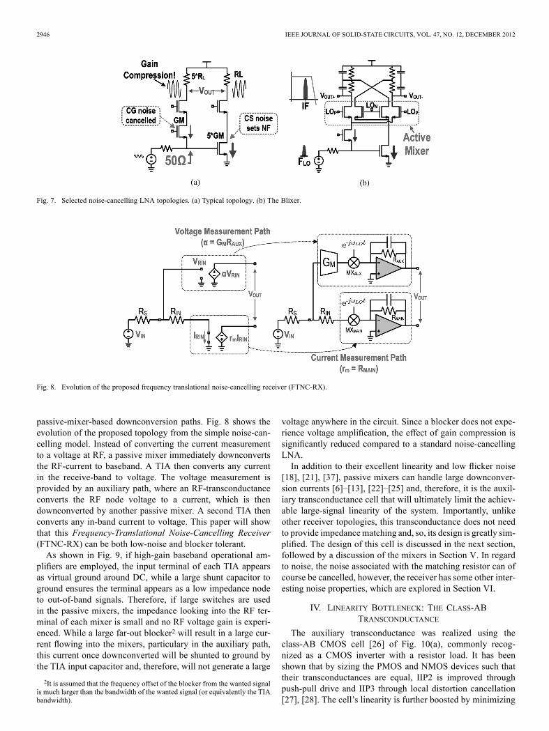
of the topology shown in Fig. 7(a). A common-gate FET
provides the real 50 impedance and the current measure-ment, while a much larger common-source FET, sized forlow input-referred noise, provides the voltage measurement.The common-gate and common-source currents (which areunequal) are then converted to balanced voltages at RF. Thedrawback to this approach is that voltage gain is present acrossa wide bandwidth and, therefore, large blockers can drive theamplifier into saturation.1
B. The Frequency-Translational Noise-Cancelling Receiver
In order to tolerate large blockers while still employing fullnoise-cancelling, this work proposes the use of two separate
1Noting that there is no requirement to generate voltages at RF, one approach[19], [20] proposes stacking an active mixer on top of the input transistors, andconverting the FET currents to voltages at a low IF (Fig. 7(b)). Although thetopology extends the receive bandwidth, the use of active mixers results in apoor NF. The topology is also unlikely to be blocker-tolerant because of tran-sistor stacking and large voltage swings at IF.
2946 IEEE JOURNAL OF SOLID-STATE CIRCUITS, VOL. 47, NO. 12, DECEMBER 2012
Fig. 7. Selected noise-cancelling LNA topologies. (a) Typical topology. (b) The Blixer.
Fig. 8. Evolution of the proposed frequency translational noise-cancelling receiver (FTNC-RX).
passive-mixer-based downconversion paths. Fig. 8 shows theevolution of the proposed topology from the simple noise-can-celling model. Instead of converting the current measurementto a voltage at RF, a passive mixer immediately downconvertsthe RF-current to baseband. A TIA then converts any currentin the receive-band to voltage. The voltage measurement isprovided by an auxiliary path, where an RF-transconductanceconverts the RF node voltage to a current, which is thendownconverted by another passive mixer. A second TIA thenconverts any in-band current to voltage. This paper will showthat this Frequency-Translational Noise-Cancelling Receiver(FTNC-RX) can be both low-noise and blocker tolerant.As shown in Fig. 9, if high-gain baseband operational am-
plifiers are employed, the input terminal of each TIA appearsas virtual ground around DC, while a large shunt capacitor toground ensures the terminal appears as a low impedance nodeto out-of-band signals. Therefore, if large switches are usedin the passive mixers, the impedance looking into the RF ter-minal of each mixer is small and no RF voltage gain is experi-enced. While a large far-out blocker2 will result in a large cur-rent flowing into the mixers, particulary in the auxiliary path,this current once downconverted will be shunted to ground bythe TIA input capacitor and, therefore, will not generate a large
2It is assumed that the frequency offset of the blocker from the wanted signalis much larger than the bandwidth of the wanted signal (or equivalently the TIAbandwidth).
voltage anywhere in the circuit. Since a blocker does not expe-rience voltage amplification, the effect of gain compression issignificantly reduced compared to a standard noise-cancellingLNA.In addition to their excellent linearity and low flicker noise
[18], [21], [37], passive mixers can handle large downconver-sion currents [6]–[13], [22]–[25] and, therefore, it is the auxil-iary transconductance cell that will ultimately limit the achiev-able large-signal linearity of the system. Importantly, unlikeother receiver topologies, this transconductance does not needto provide impedancematching and, so, its design is greatly sim-plified. The design of this cell is discussed in the next section,followed by a discussion of the mixers in Section V. In regardto noise, the noise associated with the matching resistor can ofcourse be cancelled, however, the receiver has some other inter-esting noise properties, which are explored in Section VI.
IV. LINEARITY BOTTLENECK: THE CLASS-ABTRANSCONDUCTANCE
The auxiliary transconductance was realized using theclass-AB CMOS cell [26] of Fig. 10(a), commonly recog-nized as a CMOS inverter with a resistor load. It has beenshown that by sizing the PMOS and NMOS devices such thattheir transconductances are equal, IIP2 is improved throughpush-pull drive and IIP3 through local distortion cancellation[27], [28]. The cell’s linearity is further boosted by minimizing
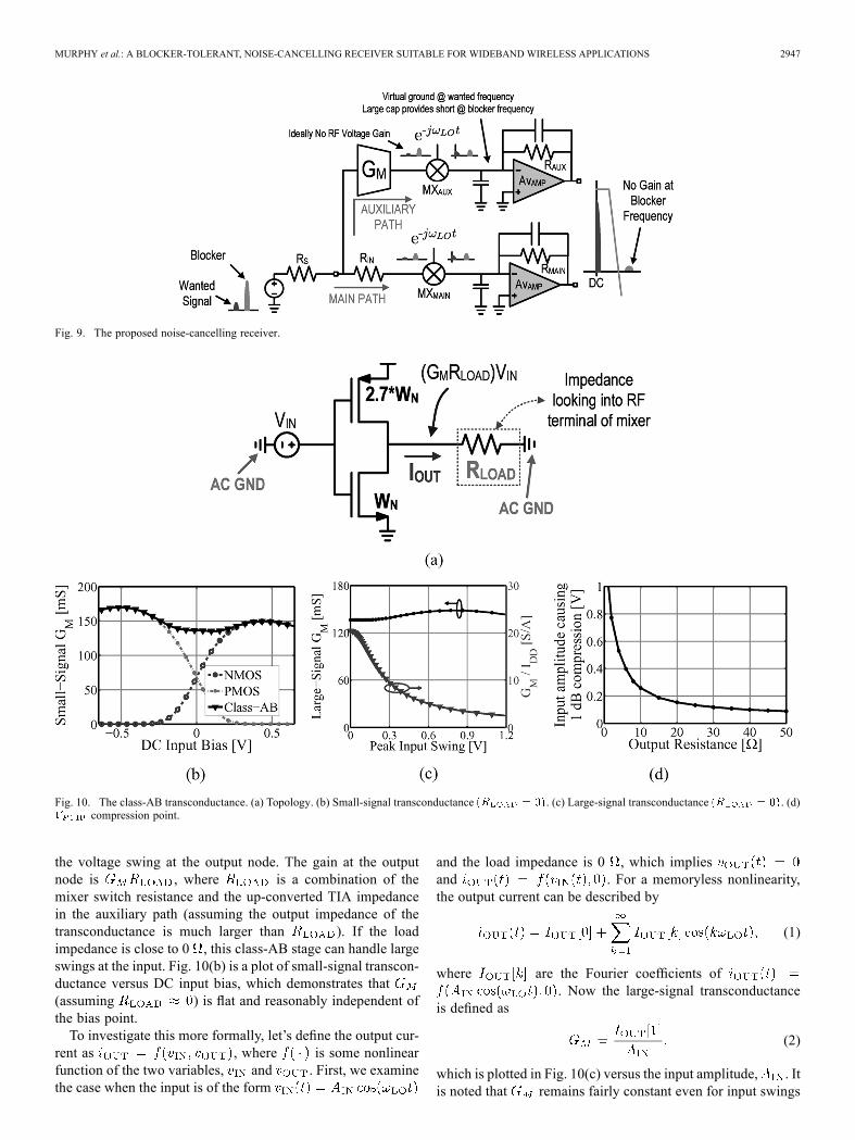
MURPHY et al.: A BLOCKER-TOLERANT, NOISE-CANCELLING RECEIVER SUITABLE FOR WIDEBAND WIRELESS APPLICATIONS 2947
Fig. 9. The proposed noise-cancelling receiver.
Fig. 10. The class-AB transconductance. (a) Topology. (b) Small-signal transconductance . (c) Large-signal transconductance . (d)compression point.
the voltage swing at the output node. The gain at the outputnode is , where is a combination of themixer switch resistance and the up-converted TIA impedancein the auxiliary path (assuming the output impedance of thetransconductance is much larger than ). If the loadimpedance is close to 0 , this class-AB stage can handle largeswings at the input. Fig. 10(b) is a plot of small-signal transcon-ductance versus DC input bias, which demonstrates that(assuming ) is flat and reasonably independent ofthe bias point.To investigate this more formally, let’s define the output cur-
rent as , where is some nonlinearfunction of the two variables, and . First, we examinethe case when the input is of the form
and the load impedance is 0 , which impliesand . For a memoryless nonlinearity,the output current can be described by
(1)
where are the Fourier coefficients of. Now the large-signal transconductance
is defined as
(2)
which is plotted in Fig. 10(c) versus the input amplitude, . Itis noted that remains fairly constant even for input swings
2948 IEEE JOURNAL OF SOLID-STATE CIRCUITS, VOL. 47, NO. 12, DECEMBER 2012
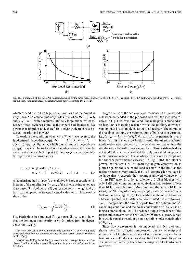
Fig. 11. Limitation of the class-AB transconductance on the large-signal linearity of the FTNC-RX. (a) Ideal FTNC-RX testbench, (b) Blocker versusthe auxiliary load resistance, (c) Blocker noise figure assuming .
which exceed the rail voltage, which implies that the circuit isvery linear.3 Of course, this only holds true whenand , which requires infinitely large mixer switches.Larger mixer switches come at the expense of increased LOpower consumption and, therefore, a clear tradeoff exists be-tween linearity and power.4
To explore the condition when , we revert to thefundamental dependence,
, which has an implicit dependenceof on . In well-behaved nonlinearities, this can bere-defined as an explicit dependence on , which can thenbe expressed as a power series
(3)
A standardmethod to specify the relative 3rd-order coefficient isin terms of the amplitude of the sinewave input voltagethat causes (defined as (2) but for non-zero ) to dropby 1 dB compared to its small signal value of . It is readilyshown that
(4)
Fig. 10(d) plots the simulated versus , and showsthat the dominant nonlinearity in arises from its depen-dance on .
3The class-AB cell is able to maintain this constant by drawing morepower and, therefore, the transconductance per unit current drops (also shownin Fig. 10(c)).4In other words, Fig. 10(b) & (c) represent the best case performance of the
class-AB cell provided one was willing to burn large amounts of current in theLO chain.
To get a sense of the achievable performance of this class-ABcell when embedded in the proposed receiver, the idealized re-ceiver in Fig. 11(a) was simulated. The main path is modeled asan ideal 50 matching resistor, while the auxiliary downcon-version path is also modeled as an ideal resistor. The output ofthe receiver is simply the weighted sum of both resistor currents,i.e., . As the main path is verylinear (in this instance perfectly linear), the antenna-referrednonlinearity measurements of the receiver are better than thestand-alone class-AB transconductance. This test-bench doesnot model downconversion, and the only non-ideal componentis the transconductance. The auxiliary resistor is then swept andthe blocker performance assessed. In Fig. 11(b), the blockerpower that causes 1 dB of small-signal gain compression isplotted against the size of the load resistor. In the limit as theresistor becomes very small, the 1 dB compression voltage isso large that it exceeds the maximum allowed voltage on a40 nm FET gate. In order to tolerate a 0 dBm blocker withonly 1 dB gain compression, an equivalent load resistor of lessthan 10 should be used. More importantly, with a 10 re-sistor, the NF degrades only very slightly in the presence of a0 dBm blocker (Fig. 11(c)). Degradation in the noise figure fora blocker greater than 0 dBm can be attributed to the following:as compresses, the circuit departs from the optimum noise-cancelling condition and the noise contribution of is nolonger completely nulled. The reduced output impedance of thetransconductance when the NMOS/PMOS transistors are forcedinto triode can also result in a non-negligible noise contributionof .Since downconversion is not modeled, this NF plot only
shows the effect of gain compression, but not of reciprocalmixing with LO phase noise nor of noise in subsequent base-band stages. But it does demonstrate that the class-AB transcon-ductance is sufficiently linear for the proposed blocker-tolerantreceiver.
MURPHY et al.: A BLOCKER-TOLERANT, NOISE-CANCELLING RECEIVER SUITABLE FOR WIDEBAND WIRELESS APPLICATIONS 2949
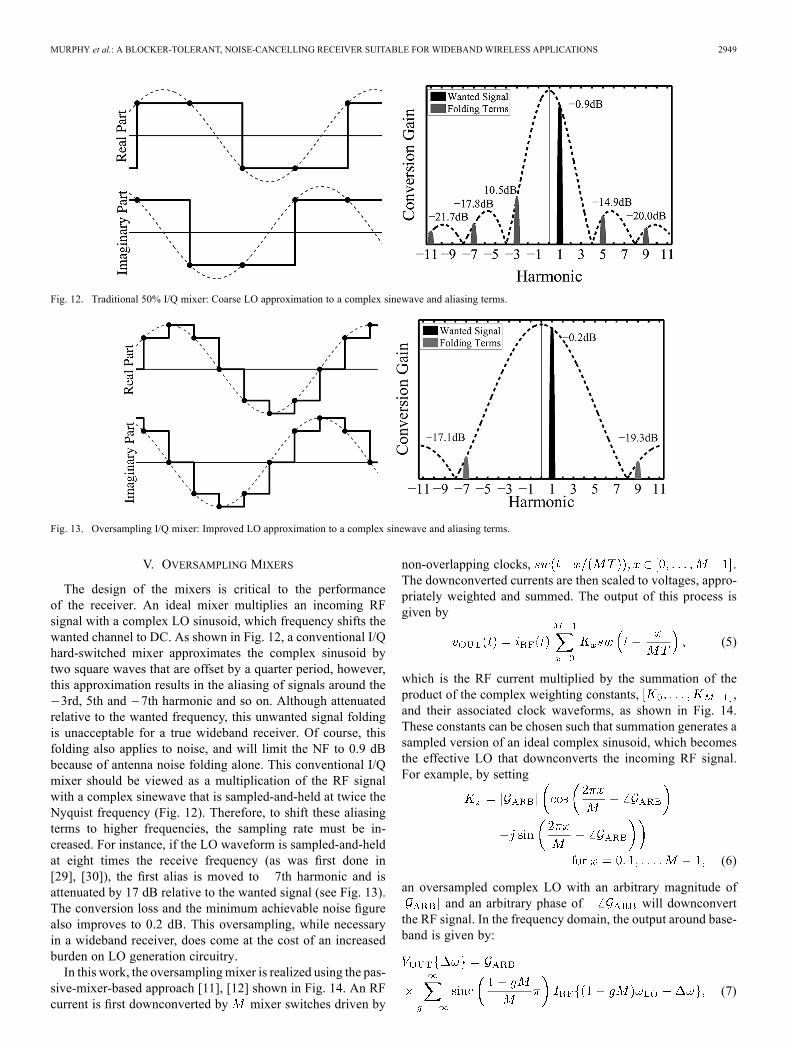
Fig. 12. Traditional 50% I/Q mixer: Coarse LO approximation to a complex sinewave and aliasing terms.
Fig. 13. Oversampling I/Q mixer: Improved LO approximation to a complex sinewave and aliasing terms.
V. OVERSAMPLING MIXERS
The design of the mixers is critical to the performanceof the receiver. An ideal mixer multiplies an incoming RFsignal with a complex LO sinusoid, which frequency shifts thewanted channel to DC. As shown in Fig. 12, a conventional I/Qhard-switched mixer approximates the complex sinusoid bytwo square waves that are offset by a quarter period, however,this approximation results in the aliasing of signals around the3rd, 5th and 7th harmonic and so on. Although attenuated
relative to the wanted frequency, this unwanted signal foldingis unacceptable for a true wideband receiver. Of course, thisfolding also applies to noise, and will limit the NF to 0.9 dBbecause of antenna noise folding alone. This conventional I/Qmixer should be viewed as a multiplication of the RF signalwith a complex sinewave that is sampled-and-held at twice theNyquist frequency (Fig. 12). Therefore, to shift these aliasingterms to higher frequencies, the sampling rate must be in-creased. For instance, if the LO waveform is sampled-and-heldat eight times the receive frequency (as was first done in[29], [30]), the first alias is moved to 7th harmonic and isattenuated by 17 dB relative to the wanted signal (see Fig. 13).The conversion loss and the minimum achievable noise figurealso improves to 0.2 dB. This oversampling, while necessaryin a wideband receiver, does come at the cost of an increasedburden on LO generation circuitry.In this work, the oversamplingmixer is realized using the pas-
sive-mixer-based approach [11], [12] shown in Fig. 14. An RFcurrent is first downconverted by mixer switches driven by
non-overlapping clocks, .The downconverted currents are then scaled to voltages, appro-priately weighted and summed. The output of this process isgiven by
(5)
which is the RF current multiplied by the summation of theproduct of the complex weighting constants, ,and their associated clock waveforms, as shown in Fig. 14.These constants can be chosen such that summation generates asampled version of an ideal complex sinusoid, which becomesthe effective LO that downconverts the incoming RF signal.For example, by setting
(6)
an oversampled complex LO with an arbitrary magnitude ofand an arbitrary phase of will downconvert
the RF signal. In the frequency domain, the output around base-band is given by:
(7)
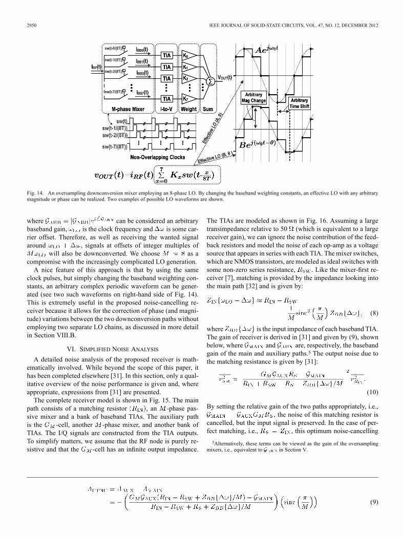
2950 IEEE JOURNAL OF SOLID-STATE CIRCUITS, VOL. 47, NO. 12, DECEMBER 2012
Fig. 14. An oversampling downconversion mixer employing an 8-phase LO. By changing the baseband weighting constants, an effective LO with any arbitrarymagnitude or phase can be realized. Two examples of possible LO waveforms are shown.
where can be considered an arbitrarybaseband gain, is the clock frequency and is some car-rier offset. Therefore, as well as receiving the wanted signalaround , signals at offsets of integer multiples of
will also be downconverted. We choose as acompromise with the increasingly complicated LO generation.A nice feature of this approach is that by using the same
clock pulses, but simply changing the baseband weighting con-stants, an arbitrary complex periodic waveform can be gener-ated (see two such waveforms on right-hand side of Fig. 14).This is extremely useful in the proposed noise-cancelling re-ceiver because it allows for the correction of phase (and magni-tude) variations between the two downconversion paths withoutemploying two separate LO chains, as discussed in more detailin Section VIII.B.
VI. SIMPLIFIED NOISE ANALYSIS
A detailed noise analysis of the proposed receiver is math-ematically involved. While beyond the scope of this paper, ithas been completed elsewhere [31]. In this section, only a qual-itative overview of the noise performance is given and, whereappropriate, expressions from [31] are presented.The complete receiver model is shown in Fig. 15. The main
path consists of a matching resistor , an -phase pas-sive mixer and a bank of baseband TIAs. The auxiliary pathis the -cell, another -phase mixer, and another bank ofTIAs. The I/Q signals are constructed from the TIA outputs.To simplify matters, we assume that the RF node is purely re-sistive and that the -cell has an infinite output impedance.
The TIAs are modeled as shown in Fig. 16. Assuming a largetransimpedance relative to 50 (which is equivalent to a largereceiver gain), we can ignore the noise contribution of the feed-back resistors and model the noise of each op-amp as a voltagesource that appears in series with each TIA. The mixer switches,which are NMOS transistors, are modeled as ideal switches withsome non-zero series resistance, . Like the mixer-first re-ceiver [7], matching is provided by the impedance looking intothe main path [32] and is given by:
(8)
where is the input impedance of each baseband TIA.The gain of receiver is derived in [31] and given by (9), shownbelow, where and are, respectively, the basebandgain of the main and auxiliary paths.5 The output noise due tothe matching resistance is given by [31]:
(10)
By setting the relative gain of the two paths appropriately, i.e.,, the noise of this matching resistor is
cancelled, but the input signal is preserved. In the case of per-fect matching, i.e., , this optimum noise-cancelling
5Alternatively, these terms can be viewed as the gain of the oversamplingmixers, i.e., equivalent to in Section V.
(9)
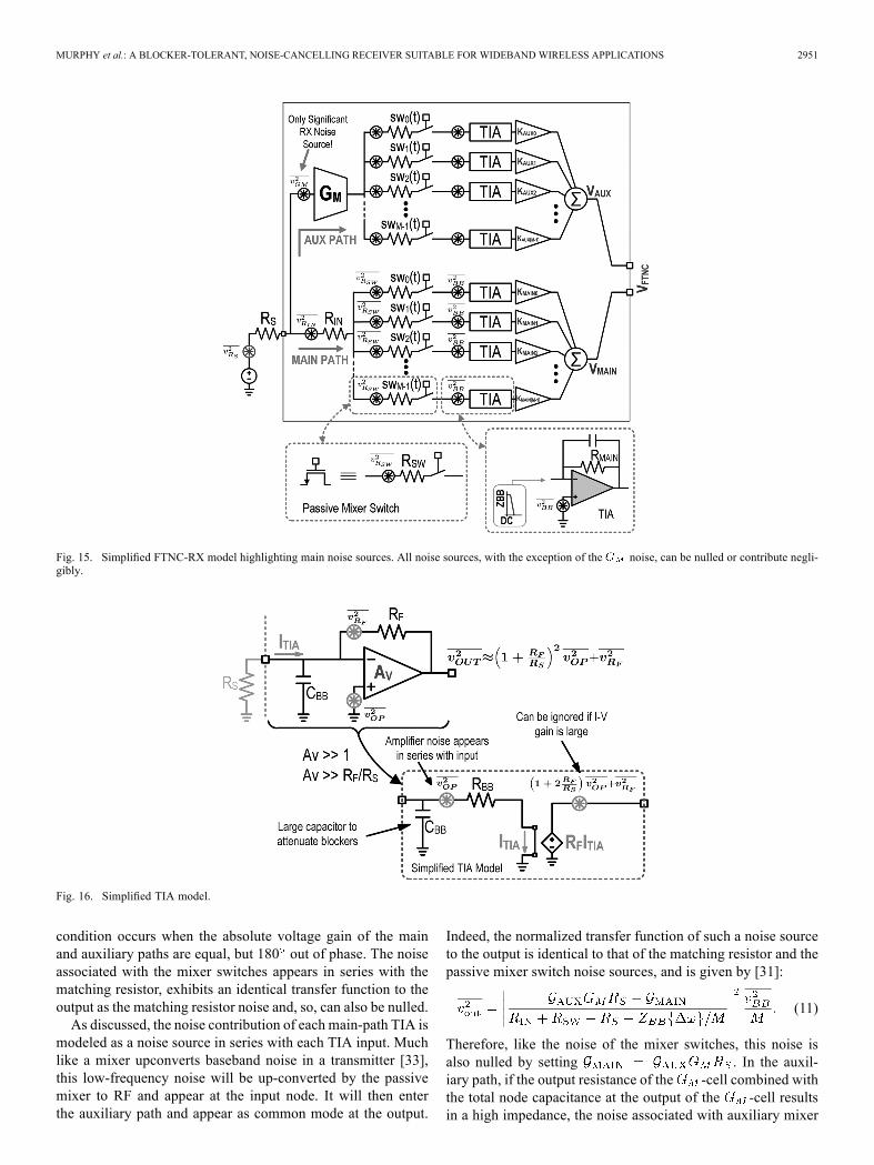
MURPHY et al.: A BLOCKER-TOLERANT, NOISE-CANCELLING RECEIVER SUITABLE FOR WIDEBAND WIRELESS APPLICATIONS 2951
Fig. 15. Simplified FTNC-RX model highlighting main noise sources. All noise sources, with the exception of the noise, can be nulled or contribute negli-gibly.
Fig. 16. Simplified TIA model.
condition occurs when the absolute voltage gain of the mainand auxiliary paths are equal, but 180 out of phase. The noiseassociated with the mixer switches appears in series with thematching resistor, exhibits an identical transfer function to theoutput as the matching resistor noise and, so, can also be nulled.As discussed, the noise contribution of each main-path TIA is
modeled as a noise source in series with each TIA input. Muchlike a mixer upconverts baseband noise in a transmitter [33],this low-frequency noise will be up-converted by the passivemixer to RF and appear at the input node. It will then enterthe auxiliary path and appear as common mode at the output.
Indeed, the normalized transfer function of such a noise sourceto the output is identical to that of the matching resistor and thepassive mixer switch noise sources, and is given by [31]:
(11)
Therefore, like the noise of the mixer switches, this noise isalso nulled by setting . In the auxil-iary path, if the output resistance of the -cell combined withthe total node capacitance at the output of the -cell resultsin a high impedance, the noise associated with auxiliary mixer
2952 IEEE JOURNAL OF SOLID-STATE CIRCUITS, VOL. 47, NO. 12, DECEMBER 2012
Fig. 17. The complete frequency-translational noise-cancelling receiver (FTNC-RX).
switches and the auxiliary op-amps will not contribute signif-icantly to the total output noise. This is because the auxiliaryTIAs are current driven, and since only one switch is on at anygiven time, the series voltage noise sources cannot generate anoise current. Therefore, when optimally configured, i.e., when
, the auxiliary transconductance is theonly significant noise contributor and largely determines the re-ceiver’s noise figure. Indeed, to a first order, the noise factor ( )is given by
(12)
where is antenna noise and, in the case of the class-AB
transconductance,. If a large number of mixer phases is employed (i.e.,
is large), the conversion gain of the passive mixers, which isgiven by the term in (12), approaches unity. There-fore, the noise factor can be made arbitrarily close to 1 by maxi-mizing the size of the auxiliary transconductance. For instance,in this work mS and , which implies thetheoretical noise figure is under 0.9 dB.Note that when the auxiliary path is powered down and noise
cancelling is disabled, the receiver behaves like an equivalentmixer-first receiver and the noise factor is given by [31]:
(13)
If is small, matching requires thatand the noise figure will be limited to 3 dB. Even if this
is not the case and the up-converted TIA input impedance isused to provide matching, noise due to the baseband TIAs willcontribute directly to the receiver’s noise figure and flicker noiseis likely to be significant. Flicker noise from the main-path TIAsis less problematic when the auxiliary path is enabled as isideally cancelled.
VII. CIRCUIT DESIGN
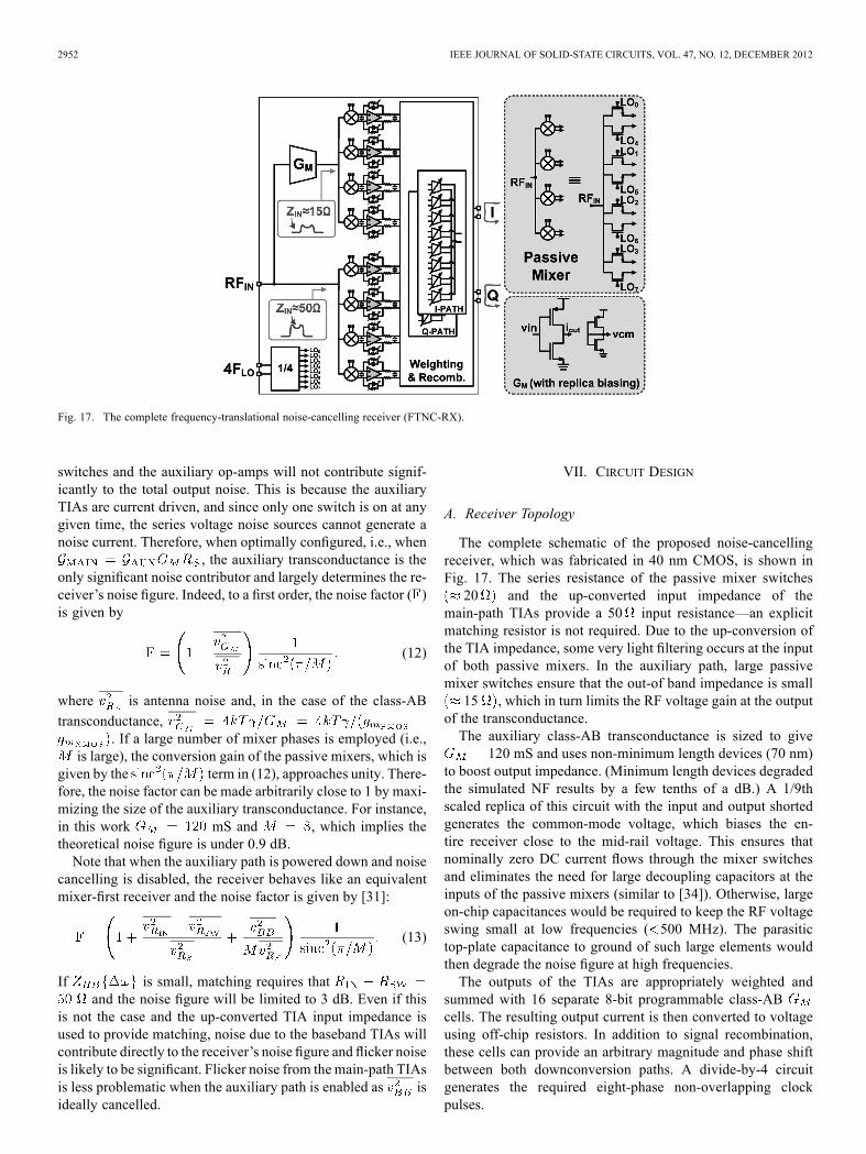
A. Receiver Topology
The complete schematic of the proposed noise-cancellingreceiver, which was fabricated in 40 nm CMOS, is shown inFig. 17. The series resistance of the passive mixer switches20 and the up-converted input impedance of the
main-path TIAs provide a 50 input resistance—an explicitmatching resistor is not required. Due to the up-conversion ofthe TIA impedance, some very light filtering occurs at the inputof both passive mixers. In the auxiliary path, large passivemixer switches ensure that the out-of band impedance is small15 , which in turn limits the RF voltage gain at the output
of the transconductance.The auxiliary class-AB transconductance is sized to give
120 mS and uses non-minimum length devices (70 nm)to boost output impedance. (Minimum length devices degradedthe simulated NF results by a few tenths of a dB.) A 1/9thscaled replica of this circuit with the input and output shortedgenerates the common-mode voltage, which biases the en-tire receiver close to the mid-rail voltage. This ensures thatnominally zero DC current flows through the mixer switchesand eliminates the need for large decoupling capacitors at theinputs of the passive mixers (similar to [34]). Otherwise, largeon-chip capacitances would be required to keep the RF voltageswing small at low frequencies ( 500 MHz). The parasitictop-plate capacitance to ground of such large elements wouldthen degrade the noise figure at high frequencies.The outputs of the TIAs are appropriately weighted and
summed with 16 separate 8-bit programmable class-ABcells. The resulting output current is then converted to voltageusing off-chip resistors. In addition to signal recombination,these cells can provide an arbitrary magnitude and phase shiftbetween both downconversion paths. A divide-by-4 circuitgenerates the required eight-phase non-overlapping clockpulses.
MURPHY et al.: A BLOCKER-TOLERANT, NOISE-CANCELLING RECEIVER SUITABLE FOR WIDEBAND WIRELESS APPLICATIONS 2953
Fig. 18. LO-to-RF noise coupling in passive mixers. (a) A single-ended and fully differential passive mixer driven with clocks containing uncorrelated phasenoise. (b) Simulated noise-figure of an ideal single-ended mixer; noise figure is corrupted by LO-to-RF coupling of the LO phase noise. (c) Simulated noise-figureof an ideal fully-differential mixer; noise figure is uncorrupted by LO phase noise.
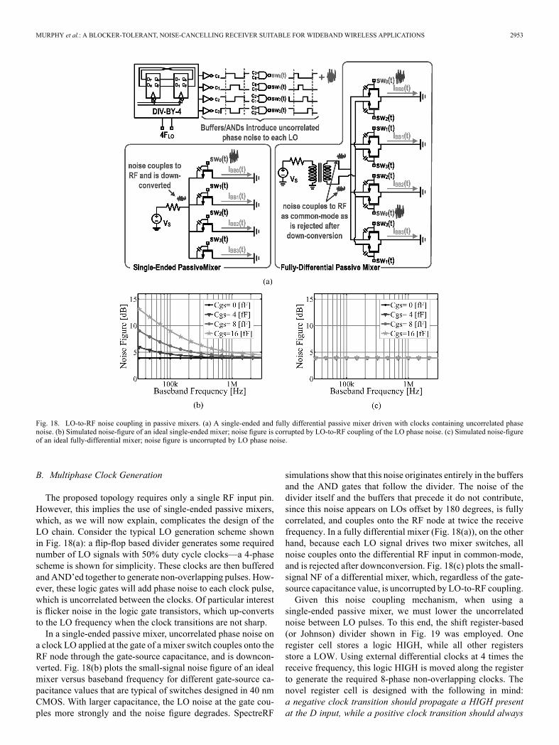
B. Multiphase Clock Generation
The proposed topology requires only a single RF input pin.However, this implies the use of single-ended passive mixers,which, as we will now explain, complicates the design of theLO chain. Consider the typical LO generation scheme shownin Fig. 18(a): a flip-flop based divider generates some requirednumber of LO signals with 50% duty cycle clocks—a 4-phasescheme is shown for simplicity. These clocks are then bufferedand AND’ed together to generate non-overlapping pulses. How-ever, these logic gates will add phase noise to each clock pulse,which is uncorrelated between the clocks. Of particular interestis flicker noise in the logic gate transistors, which up-convertsto the LO frequency when the clock transitions are not sharp.In a single-ended passive mixer, uncorrelated phase noise on
a clock LO applied at the gate of a mixer switch couples onto theRF node through the gate-source capacitance, and is downcon-verted. Fig. 18(b) plots the small-signal noise figure of an idealmixer versus baseband frequency for different gate-source ca-pacitance values that are typical of switches designed in 40 nmCMOS. With larger capacitance, the LO noise at the gate cou-ples more strongly and the noise figure degrades. SpectreRF
simulations show that this noise originates entirely in the buffersand the AND gates that follow the divider. The noise of thedivider itself and the buffers that precede it do not contribute,since this noise appears on LOs offset by 180 degrees, is fullycorrelated, and couples onto the RF node at twice the receivefrequency. In a fully differential mixer (Fig. 18(a)), on the otherhand, because each LO signal drives two mixer switches, allnoise couples onto the differential RF input in common-mode,and is rejected after downconversion. Fig. 18(c) plots the small-signal NF of a differential mixer, which, regardless of the gate-source capacitance value, is uncorrupted by LO-to-RF coupling.Given this noise coupling mechanism, when using a
single-ended passive mixer, we must lower the uncorrelatednoise between LO pulses. To this end, the shift register-based(or Johnson) divider shown in Fig. 19 was employed. Oneregister cell stores a logic HIGH, while all other registersstore a LOW. Using external differential clocks at 4 times thereceive frequency, this logic HIGH is moved along the registerto generate the required 8-phase non-overlapping clocks. Thenovel register cell is designed with the following in mind:a negative clock transition should propagate a HIGH presentat the D input, while a positive clock transition should always
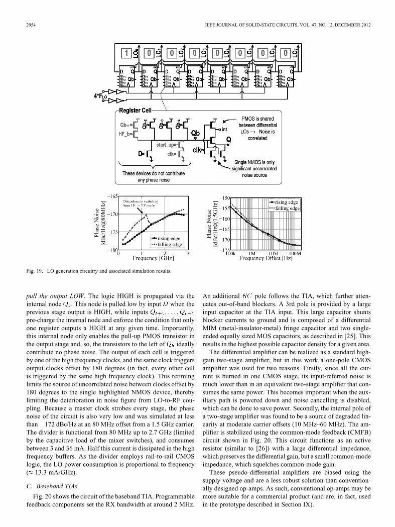
2954 IEEE JOURNAL OF SOLID-STATE CIRCUITS, VOL. 47, NO. 12, DECEMBER 2012
Fig. 19. LO generation circuitry and associated simulation results.
pull the output LOW. The logic HIGH is propagated via theinternal node . This node is pulled low by input when theprevious stage output is HIGH, while inputspre-charge the internal node and enforce the condition that onlyone register outputs a HIGH at any given time. Importantly,this internal node only enables the pull-up PMOS transistor inthe output stage and, so, the transistors to the left of ideallycontribute no phase noise. The output of each cell is triggeredby one of the high frequency clocks, and the same clock triggersoutput clocks offset by 180 degrees (in fact, every other cellis triggered by the same high frequency clock). This retiminglimits the source of uncorrelated noise between clocks offset by180 degrees to the single highlighted NMOS device, therebylimiting the deterioration in noise figure from LO-to-RF cou-pling. Because a master clock strobes every stage, the phasenoise of the circuit is also very low and was simulated at lessthan 172 dBc/Hz at an 80 MHz offset from a 1.5 GHz carrier.The divider is functional from 80 MHz up to 2.7 GHz (limitedby the capacitive load of the mixer switches), and consumesbetween 3 and 36 mA. Half this current is dissipated in the highfrequency buffers. As the divider employs rail-to-rail CMOSlogic, the LO power consumption is proportional to frequency( 13.3 mA/GHz).
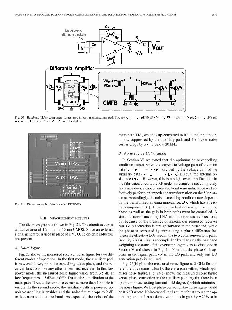
C. Baseband TIAs
Fig. 20 shows the circuit of the baseband TIA. Programmablefeedback components set the RX bandwidth at around 2 MHz.
An additional pole follows the TIA, which further atten-uates out-of-band blockers. A 3rd pole is provided by a largeinput capacitor at the TIA input. This large capacitor shuntsblocker currents to ground and is composed of a differentialMIM (metal-insulator-metal) fringe capacitor and two single-ended equally sized MOS capacitors, as described in [25]. Thisresults in the highest possible capacitor density for a given area.The differential amplifier can be realized as a standard high-
gain two-stage amplifier, but in this work a one-pole CMOSamplifier was used for two reasons. Firstly, since all the cur-rent is burned in one CMOS stage, its input-referred noise ismuch lower than in an equivalent two-stage amplifier that con-sumes the same power. This becomes important when the aux-iliary path is powered down and noise cancelling is disabled,which can be done to save power. Secondly, the internal pole ofa two-stage amplifier was found to be a source of degraded lin-earity at moderate carrier offsets (10 MHz–60 MHz). The am-plifier is stabilized using the common-mode feedback (CMFB)circuit shown in Fig. 20. This circuit functions as an activeresistor (similar to [26]) with a large differential impedance,which preserves the differential gain, but a small common-modeimpedance, which squelches common-mode gain.These pseudo-differential amplifiers are biased using the
supply voltage and are a less robust solution than convention-ally designed op-amps. As such, conventional op-amps may bemore suitable for a commercial product (and are, in fact, usedin the prototype described in Section IX).
MURPHY et al.: A BLOCKER-TOLERANT, NOISE-CANCELLING RECEIVER SUITABLE FOR WIDEBAND WIRELESS APPLICATIONS 2955
Fig. 20. Baseband TIAs (component values used in each main/auxiliary path TIA are: pF/90 pF, – pF/ – pF, pF/8 pF,– k /1.5–9.5 k k /2k ).
Fig. 21. Die micrograph of single-ended FTNC-RX.
VIII. MEASUREMENT RESULTS
The die micrograph is shown in Fig. 21. The circuit occupiesan active area of 1.2 mm in 40 nm CMOS. Since an externalsignal generator is used in place of a VCO, no on-chip inductorsare present.
A. Noise Figure
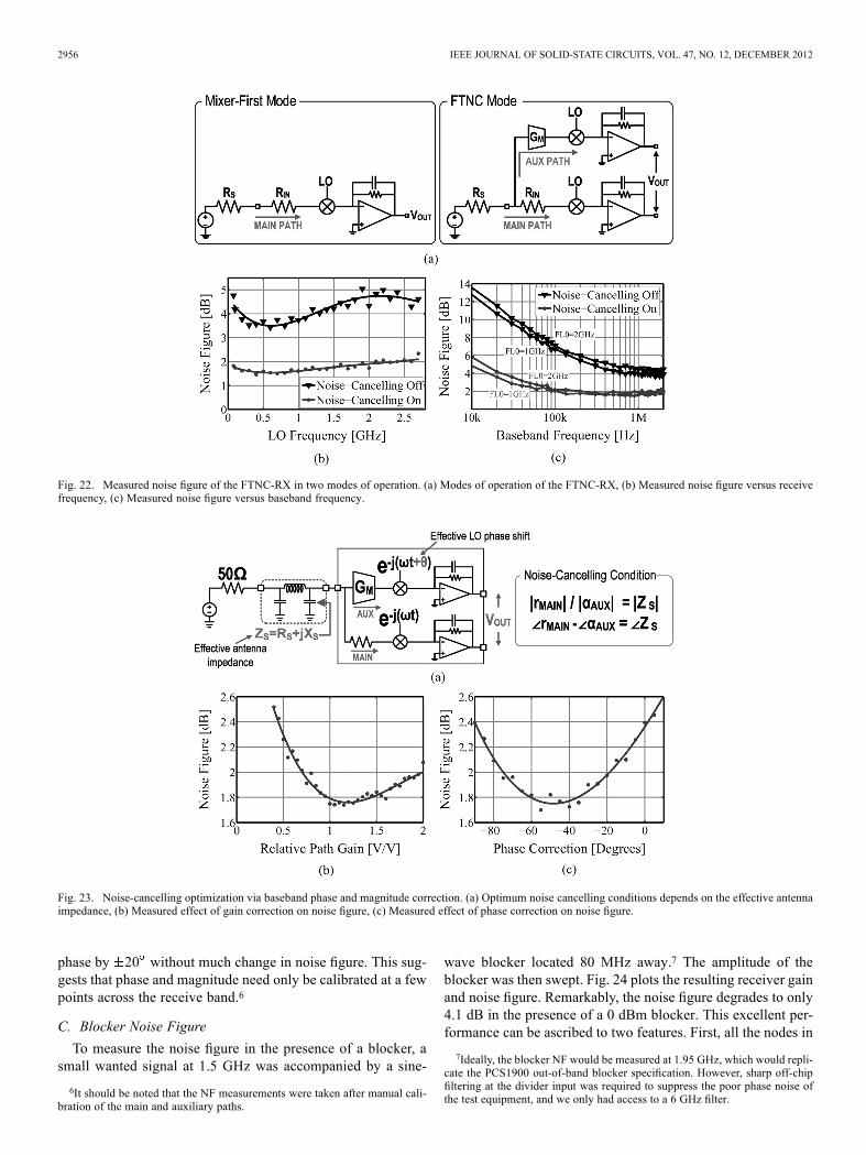
Fig. 22 shows the measured receiver noise figure for two dif-ferent modes of operation. In the first mode, the auxiliary pathis powered down, no noise-cancelling takes place, and the re-ceiver functions like any other mixer-first receiver. In this lowpower mode, the measured noise figure varies from 3.5 dB atlow frequencies to 5 dB at 2 GHz. Due to the contribution of themain-path TIAs, a flicker noise corner at more than 100 kHz isvisible. In the second-mode, the auxiliary path is powered up,noise-cancelling is enabled and the noise figure drops to 2 dBor less across the entire band. As expected, the noise of the
main-path TIA, which is up-converted to RF at the input node,is now suppressed by the auxiliary path and the flicker noisecorner drops by 5 to below 20 kHz.
B. Noise Figure Optimization
In Section VI we stated that the optimum noise-cancellingcondition occurs when the current-to-voltage gain of the mainpath divided by the voltage gain of theauxiliary path is equal the antenna re-sistance . However, this is a slight oversimplification: Inthe fabricated circuit, the RF node impedance is not completelyreal since device capacitance and bond wire inductance will ef-fectively perform an impedance transformation on the 50 an-tenna. Accordingly, the noise-cancelling condition now dependson the transformed antenna impedance, , which has a reac-tive component [31]. Therefore, for best noise-suppression, thephase as well as the gain in both paths must be controlled. Astandard noise-cancelling LNA cannot make such corrections,but because of the presence of mixers, our proposed receivercan. Gain correction is straightforward in the baseband, whilethe phase is corrected by introducing a phase difference be-tween the effective LOs used in the two downconversions paths(see Fig. 23(a)). This is accomplished by changing the basebandweighting constants of the oversampling mixers as discussed inSection V and shown in Fig. 14. Note that the phase shift ap-pears in the signal path, not in the LO path, and only one LOgeneration path is required.Fig. 23(b) plots the measured noise figure at 2 GHz for dif-
ferent relative gains. Clearly, there is a gain setting which opti-mizes noise figure. Fig. 23(c) shows the measured noise figureversus phase correction in the auxiliary path. Again, there is anoptimum phase setting (around 45 degrees) which minimizesthe noise figure.Without phase correction the noise figure wouldbe 0.6 dB worse. Noise-cancelling is quite robust around the op-timum point, and can tolerate variations in gain by 20% or in
2956 IEEE JOURNAL OF SOLID-STATE CIRCUITS, VOL. 47, NO. 12, DECEMBER 2012
Fig. 22. Measured noise figure of the FTNC-RX in two modes of operation. (a) Modes of operation of the FTNC-RX, (b) Measured noise figure versus receivefrequency, (c) Measured noise figure versus baseband frequency.
Fig. 23. Noise-cancelling optimization via baseband phase and magnitude correction. (a) Optimum noise cancelling conditions depends on the effective antennaimpedance, (b) Measured effect of gain correction on noise figure, (c) Measured effect of phase correction on noise figure.
phase by 20 without much change in noise figure. This sug-gests that phase and magnitude need only be calibrated at a fewpoints across the receive band.6
C. Blocker Noise Figure
To measure the noise figure in the presence of a blocker, asmall wanted signal at 1.5 GHz was accompanied by a sine-
6It should be noted that the NF measurements were taken after manual cali-bration of the main and auxiliary paths.
wave blocker located 80 MHz away.7 The amplitude of theblocker was then swept. Fig. 24 plots the resulting receiver gainand noise figure. Remarkably, the noise figure degrades to only4.1 dB in the presence of a 0 dBm blocker. This excellent per-formance can be ascribed to two features. First, all the nodes in
7Ideally, the blocker NF would be measured at 1.95 GHz, which would repli-cate the PCS1900 out-of-band blocker specification. However, sharp off-chipfiltering at the divider input was required to suppress the poor phase noise ofthe test equipment, and we only had access to a 6 GHz filter.
MURPHY et al.: A BLOCKER-TOLERANT, NOISE-CANCELLING RECEIVER SUITABLE FOR WIDEBAND WIRELESS APPLICATIONS 2957
Fig. 24. Measured receiver gain and noise figure assuming a wanted signal at 1.5 GHz accompanied by a 1.58 GHz continuous-wave blocker.
Fig. 25. Measured receiver linearity at GHz. (a) Measured blocker with blocker located at , (b) Measured IIP3 using two-tone test( kHz), (c) Measured IIP2 using two-tone test ( kHz).
the system experience little or no voltage gain at the blocker fre-quency and, therefore, gain compression is limited. Second, thedivider exhibited very low phase noise, which keeps the dele-terious effect of reciprocal mixing small. In the presence of a0 dBm blocker, we suspect that the effect of reciprocal mixingis dominant, while the sharp deterioration in noise figure for ablocker in excess of 0 dBm is due to the collapse of receivergain.This prototype does not include an on-chip synthesizer,
which is required in any complete transceiver solution. In orderto maintain this blocker NF without RF filtering, the synthesizerwould require a very low-noise VCO, which will translate intoincreased VCO current consumption. Furthermore, to makeuse of the receiver’s wideband functionality, the synthesizershould be capable of generating frequencies from 320 MHz upto 10.8 GHz.
D. Linearity
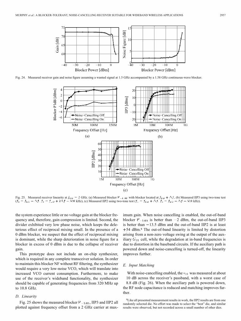
Fig. 25 shows the measured blocker , IIP3 and IIP2 allplotted against frequency offset from a 2 GHz carrier at max-
imum gain. When noise cancelling is enabled, the out-of-bandblocker is better than 2 dBm, the out-of-band IIP3is better than 13.5 dBm and the out-of-band IIP2 is at least54 dBm.8 The out-of-band linearity is limited by distortion
arising from a non-zero voltage swing at the output of the aux-iliary cell, while the degradation at in-band frequencies isdue to distortion in the baseband circuits. If the auxiliary path ispowered down and noise-cancelling is turned-off, the linearityimproves further.
E. Input Matching
With noise-cancelling enabled, the was measured at about10 dB across the receiver’s passband, with a worst case of8.8 dB (Fig. 26). When the auxiliary path is powered down,
the RF node capacitance is reduced and matching improves fur-ther.
8Like all presented measurement results in work, the IIP2 results are from onerandomly selected die. No effort was made to select the “best” die, and similarresults were observed, but not recorded across a small number of other dies.
2958 IEEE JOURNAL OF SOLID-STATE CIRCUITS, VOL. 47, NO. 12, DECEMBER 2012
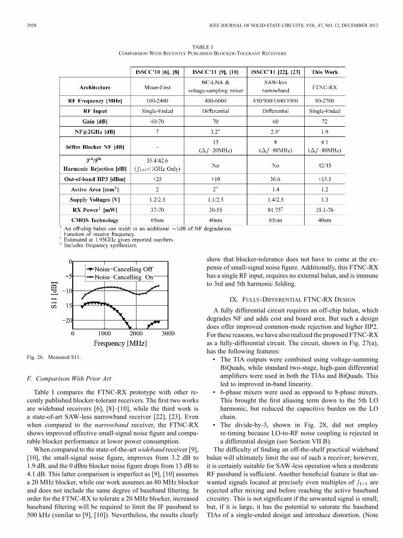
TABLE ICOMPARISON WITH RECENTLY PUBLISHED BLOCKER-TOLERANT RECEIVERS
Fig. 26. Measured S11.
F. Comparison With Prior Art
Table I compares the FTNC-RX prototype with other re-cently published blocker-tolerant receivers. The first two worksare wideband receivers [6], [8]–[10], while the third work isa state-of-art SAW-less narrowband receiver [22], [23]. Evenwhen compared to the narrowband receiver, the FTNC-RXshows improved effective small-signal noise figure and compa-rable blocker performance at lower power consumption.When compared to the state-of-the-art wideband receiver [9],
[10], the small-signal noise figure, improves from 3.2 dB to1.9 dB, and the 0 dBm blocker noise figure drops from 13 dB to4.1 dB. This latter comparison is imperfect as [9], [10] assumesa 20 MHz blocker, while our work assumes an 80 MHz blockerand does not include the same degree of baseband filtering. Inorder for the FTNC-RX to tolerate a 20 MHz blocker, increasedbaseband filtering will be required to limit the IF passband to500 kHz (similar to [9], [10]). Nevertheless, the results clearly
show that blocker-tolerance does not have to come at the ex-pense of small-signal noise figure. Additionally, this FTNC-RXhas a single RF input, requires no external balun, and is immuneto 3rd and 5th harmonic folding.
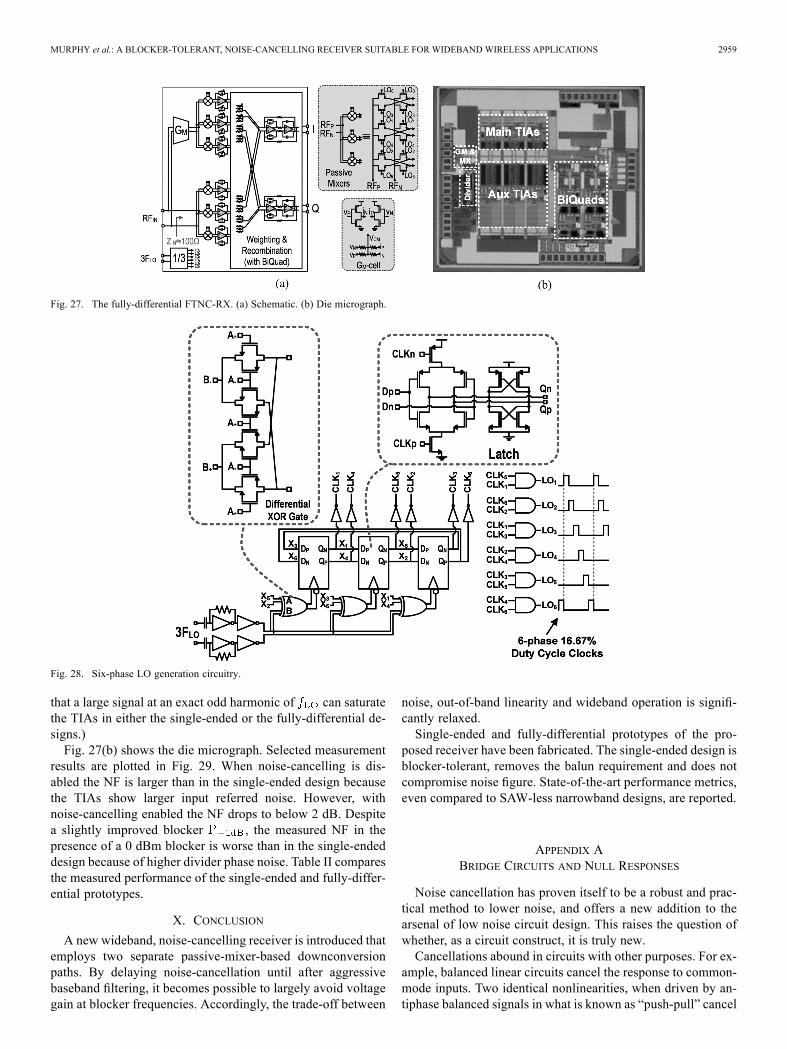
IX. FULLY-DIFFERENTIAL FTNC-RX DESIGN
A fully differential circuit requires an off-chip balun, whichdegrades NF and adds cost and board area. But such a designdoes offer improved common-mode rejection and higher IIP2.For these reasons, we have also realized the proposed FTNC-RXas a fully-differential circuit. The circuit, shown in Fig. 27(a),has the following features:• The TIA outputs were combined using voltage-summingBiQuads, while standard two-stage, high-gain differentialamplifiers were used in both the TIAs and BiQuads. Thisled to improved in-band linearity.
• 6-phase mixers were used as opposed to 8-phase mixers.This brought the first aliasing term down to the 5th LOharmonic, but reduced the capacitive burden on the LOchain.
• The divide-by-3, shown in Fig. 28, did not employre-timing because LO-to-RF noise coupling is rejected ina differential design (see Section VII.B).
The difficulty of finding an off-the-shelf practical widebandbalun will ultimately limit the use of such a receiver; however,it is certainly suitable for SAW-less operation when a moderateRF passband is sufficient. Another beneficial feature is that un-wanted signals located at precisely even multiples of arerejected after mixing and before reaching the active basebandcircuitry. This is not significant if the unwanted signal is small,but, if it is large, it has the potential to saturate the basebandTIAs of a single-ended design and introduce distortion. (Note
MURPHY et al.: A BLOCKER-TOLERANT, NOISE-CANCELLING RECEIVER SUITABLE FOR WIDEBAND WIRELESS APPLICATIONS 2959
Fig. 27. The fully-differential FTNC-RX. (a) Schematic. (b) Die micrograph.
Fig. 28. Six-phase LO generation circuitry.
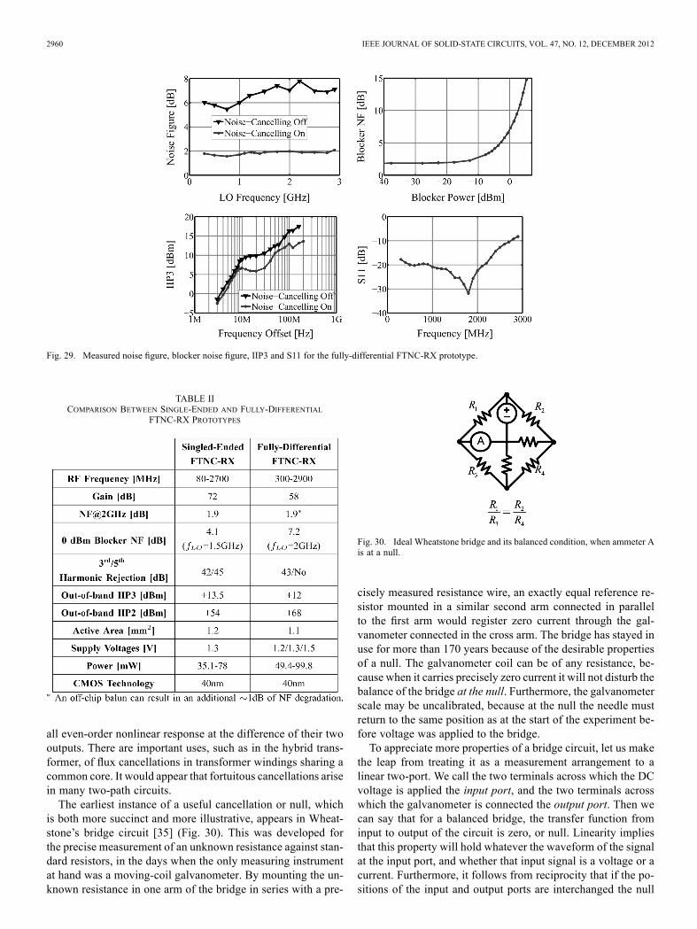
that a large signal at an exact odd harmonic of can saturatethe TIAs in either the single-ended or the fully-differential de-signs.)Fig. 27(b) shows the die micrograph. Selected measurement
results are plotted in Fig. 29. When noise-cancelling is dis-abled the NF is larger than in the single-ended design becausethe TIAs show larger input referred noise. However, withnoise-cancelling enabled the NF drops to below 2 dB. Despitea slightly improved blocker , the measured NF in thepresence of a 0 dBm blocker is worse than in the single-endeddesign because of higher divider phase noise. Table II comparesthe measured performance of the single-ended and fully-differ-ential prototypes.
X. CONCLUSION
A new wideband, noise-cancelling receiver is introduced thatemploys two separate passive-mixer-based downconversionpaths. By delaying noise-cancellation until after aggressivebaseband filtering, it becomes possible to largely avoid voltagegain at blocker frequencies. Accordingly, the trade-off between
noise, out-of-band linearity and wideband operation is signifi-cantly relaxed.Single-ended and fully-differential prototypes of the pro-
posed receiver have been fabricated. The single-ended design isblocker-tolerant, removes the balun requirement and does notcompromise noise figure. State-of-the-art performance metrics,even compared to SAW-less narrowband designs, are reported.
APPENDIX ABRIDGE CIRCUITS AND NULL RESPONSES
Noise cancellation has proven itself to be a robust and prac-tical method to lower noise, and offers a new addition to thearsenal of low noise circuit design. This raises the question ofwhether, as a circuit construct, it is truly new.Cancellations abound in circuits with other purposes. For ex-
ample, balanced linear circuits cancel the response to common-mode inputs. Two identical nonlinearities, when driven by an-tiphase balanced signals in what is known as “push-pull” cancel
2960 IEEE JOURNAL OF SOLID-STATE CIRCUITS, VOL. 47, NO. 12, DECEMBER 2012
Fig. 29. Measured noise figure, blocker noise figure, IIP3 and S11 for the fully-differential FTNC-RX prototype.
TABLE IICOMPARISON BETWEEN SINGLE-ENDED AND FULLY-DIFFERENTIAL
FTNC-RX PROTOTYPES
all even-order nonlinear response at the difference of their twooutputs. There are important uses, such as in the hybrid trans-former, of flux cancellations in transformer windings sharing acommon core. It would appear that fortuitous cancellations arisein many two-path circuits.The earliest instance of a useful cancellation or null, which
is both more succinct and more illustrative, appears in Wheat-stone’s bridge circuit [35] (Fig. 30). This was developed forthe precise measurement of an unknown resistance against stan-dard resistors, in the days when the only measuring instrumentat hand was a moving-coil galvanometer. By mounting the un-known resistance in one arm of the bridge in series with a pre-
Fig. 30. Ideal Wheatstone bridge and its balanced condition, when ammeter Ais at a null.
cisely measured resistance wire, an exactly equal reference re-sistor mounted in a similar second arm connected in parallelto the first arm would register zero current through the gal-vanometer connected in the cross arm. The bridge has stayed inuse for more than 170 years because of the desirable propertiesof a null. The galvanometer coil can be of any resistance, be-cause when it carries precisely zero current it will not disturb thebalance of the bridge at the null. Furthermore, the galvanometerscale may be uncalibrated, because at the null the needle mustreturn to the same position as at the start of the experiment be-fore voltage was applied to the bridge.To appreciate more properties of a bridge circuit, let us make
the leap from treating it as a measurement arrangement to alinear two-port. We call the two terminals across which the DCvoltage is applied the input port, and the two terminals acrosswhich the galvanometer is connected the output port. Then wecan say that for a balanced bridge, the transfer function frominput to output of the circuit is zero, or null. Linearity impliesthat this property will hold whatever the waveform of the signalat the input port, and whether that input signal is a voltage or acurrent. Furthermore, it follows from reciprocity that if the po-sitions of the input and output ports are interchanged the null
MURPHY et al.: A BLOCKER-TOLERANT, NOISE-CANCELLING RECEIVER SUITABLE FOR WIDEBAND WIRELESS APPLICATIONS 2961
Fig. 31. Null condition for another stimulus-response pair.
transfer function will remain. For this reason the two ports aretermed conjugate ports [36].If we associate resistances with the input and output ports
and suppress all sources, the bridge follows the graph of a fullyconnected star network. It follows from symmetry (which maybe difficult to appreciate when it is drawn as a non-planar graph)that for every branch into which a voltage source is inserted witha pliers entry, or a current source with a soldering-iron entry,there is another branch that will be conjugate to it provided thebridge is balanced. Fig. 31 illustrates an example.When the bridge network is generalized by introducing uni-
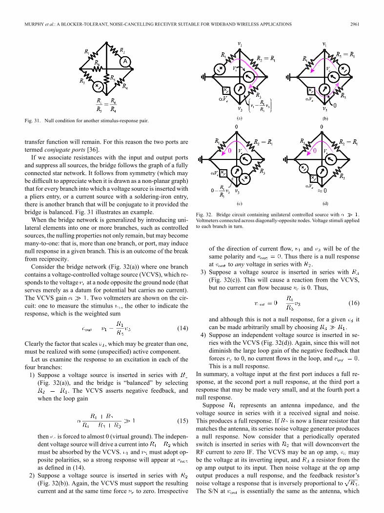
lateral elements into one or more branches, such as controlledsources, the nulling properties not only remain, but may becomemany-to-one: that is, more than one branch, or port, may inducenull response in a given branch. This is an outcome of the breakfrom reciprocity.Consider the bridge network (Fig. 32(a)) where one branch
contains a voltage-controlled voltage source (VCVS), which re-sponds to the voltage at a node opposite the ground node (thatserves merely as a datum for potential but carries no current).The VCVS gain . Two voltmeters are shown on the cir-cuit: one to measure the stimulus , the other to indicate theresponse, which is the weighted sum
(14)
Clearly the factor that scales , which may be greater than one,must be realized with some (unspecified) active component.Let us examine the response to an excitation in each of the
four branches:1) Suppose a voltage source is inserted in series with(Fig. 32(a)), and the bridge is “balanced” by selecting
. The VCVS asserts negative feedback, andwhen the loop gain
(15)
then is forced to almost 0 (virtual ground). The indepen-dent voltage source will drive a current into whichmust be absorbed by the VCVS. and must adopt op-posite polarities, so a strong response will appear atas defined in (14).
2) Suppose a voltage source is inserted in series with(Fig. 32(b)). Again, the VCVS must support the resultingcurrent and at the same time force to zero. Irrespective
Fig. 32. Bridge circuit containing unilateral controlled source with .Voltmeters connected across diagonally-opposite nodes. Voltage stimuli appliedto each branch in turn.
of the direction of current flow, and will be of thesame polarity and . Thus there is a null responseat to any voltage in series with .
3) Suppose a voltage source is inserted in series with(Fig. 32(c)). This will cause a reaction from the VCVS,but no current can flow because is 0. Thus,
(16)
and although this is not a null response, for a given itcan be made arbitrarily small by choosing .
4) Suppose an independent voltage source is inserted in se-ries with the VCVS (Fig. 32(d)). Again, since this will notdiminish the large loop gain of the negative feedback thatforces to 0, no current flows in the loop, and .This is a null response.
In summary, a voltage input at the first port induces a full re-sponse, at the second port a null response, at the third port aresponse that may be made very small, and at the fourth port anull response.Suppose represents an antenna impedance, and the
voltage source in series with it a received signal and noise.This produces a full response. If is now a linear resistor thatmatches the antenna, its series noise voltage generator producesa null response. Now consider that a periodically operatedswitch is inserted in series with that will downconvert theRF current to zero IF. The VCVS may be an op amp, maybe the voltage at its inverting input, and a resistor from theop amp output to its input. Then noise voltage at the op ampoutput produces a null response, and the feedback resistor’snoise voltage a response that is inversely proportional to .The S/N at is essentially the same as the antenna, which
2962 IEEE JOURNAL OF SOLID-STATE CIRCUITS, VOL. 47, NO. 12, DECEMBER 2012
suggests a noise figure approaching 0 dB. However, the scalefactor will require an amplifier which will introduceits own noise into . Since this amplifier is outside thepath taken by the antenna current, it can be designed to intro-duce very low noise of its own without affecting impedancematching. A mixer switch must also precede this amplifier.The reader will have noted that the foregoing text describes
the noise cancelling receiver of this paper. The concept of noisecancellation may be thought of as the result of a bridge circuitbeing automatically balanced to a null.
REFERENCES
[1] F. Bruccoleri, E. Klumperink, and B. Nauta, “Noise cancelling in wide-band CMOS LNAs,” in IEEE ISSCC Dig. 2002, pp. 406–407.
[2] F. Bruccoleri, E. Klumperink, and B. Nauta, “Wide-band CMOS low-noise amplifier exploiting thermal noise canceling,” IEEE J. Solid-State Circuits, vol. 39, no. 2, pp. 275–282, Feb. 2004.
[3] R. Bagheri, A.Mirzaei, S. Chehrazi,M. Heidari,M. Lee,M.Mikhemar,M. Tang, and A. Abidi, “An 800 MHz to 5 GHz software-defined radioreceiver in 90 nm CMOS,” in IEEE ISSCC Dig. 2006, pp. 1932–1941.
[4] R. Bagheri, A.Mirzaei, S. Chehrazi,M. Heidari,M. Lee,M.Mikhemar,W. Tang, and A. Abidi, “An 800-MHz–6-GHz software-defined wire-less receiver in 90-nm CMOS,” IEEE J. Solid-State Circuits, vol. 41,no. 12, pp. 2860–2876, Dec. 2006.
[5] A. Abidi, “The path to the software-defined radio receiver,” IEEE J.Solid-State Circuits, vol. 42, no. 5, pp. 954–966, May 2007.
[6] C. Andrews and A. Molnar, “A passive-mixer-first receiver with base-band-controlled RF impedance matching, 6 dB NF, and 27 dBmwideband IIP3,” in IEEE ISSCC Dig. 2010, pp. 46–47.
[7] C. Andrews and A. Molnar, “Implications of passive mixer trans-parency for impedance matching and noise figure in passive mixer-firstreceivers,” IEEE Trans. Circuits Syst. I, vol. 57, no. 12, pp. 3092–3103,Dec. 2010.
[8] C. Andrews and A. Molnar, “A passive mixer-first receiver with digi-tally controlled and widely tunable RF interface,” IEEE J. Solid-StateCircuits, vol. 45, no. 12, pp. 2696–2708, Dec. 2010.
[9] J. Borremans, G. Mandal, V. Giannini, T. Sano, M. Ingels, B. Ver-bruggen, and J. Craninckx, “A 40 nm CMOS highly linear 0.4-to-6GHz receiver resilient to 0 dBm out-of-band blockers,” in IEEE ISSCCDig. 2011, pp. 62–64.
[10] J. Borremans, G.Mandal, V. Giannini, B. Debaillie,M. Ingels, T. Sano,B. Verbruggen, and J. Craninckx, “A 40 nmCMOS 0.4–6 GHz receiverresilient to out-of-band blockers,” IEEE J. Solid-State Circuits, vol. 46,no. 7, pp. 1659–1671, July 2011.
[11] Z. Ru, E. Klumperink, G. Wienk, and B. Nauta, “A software-definedradio receiver architecture robust to out-of-band interference,” in IEEEISSCC Dig. 2009, pp. 230–231, 231a.
[12] Z. Ru, N. Moseley, E. Klumperink, and B. Nauta, “Digitally enhancedsoftware-defined radio receiver robust to out-of-band interference,”IEEE J. Solid-State Circuits, vol. 44, no. 12, pp. 3359–3375, Dec.2009.
[13] Z. Ru, “Frequency translation techniques for interference-robust soft-ware-defined radio receivers,” Ph.D. dissertation, Univ. of Twente, En-schede, The Netherlands, Nov. 2009.
[14] D. Murphy, A. Hafez, A. Mirzaei, M. Mikhemar, H. Darabi, M.-C.Chang, and A. Abidi, “A blocker-tolerant wideband noise-cancellingreceiver with a 2 dB noise figure,” in IEEE ISSCC Dig. 2012, pp.74–75.
[15] M. Soer, E. Klumperink, Z. Ru, F. van Vliet, and B. Nauta, “A0.2-to-2.0 GHz 65 nm CMOS receiver without LNA achieving 11dBm IIP3 and 6.5 dB NF,” in IEEE ISSCC Dig. 2009, pp. 222–223,223a.
[16] L. Franks and I. Sandberg, “An alternative approach to the realizationsof network functions: N-path filter,” Bell Syst. Tech. J., pp. 1321–1350,1960.
[17] D. von Grunigen, R. Sigg, J. Schmid, G. Moschytz, and H. Melchior,“An integrated CMOS switched-capacitor bandpass filter based onN-path and frequency-sampling principles,” IEEE J. Solid-StateCircuits, vol. SSC-18, no. 6, pp. 753–761, Dec. 1983.
[18] E. Sacchi, I. Bietti, S. Erba, L. Tee, P. Vilmercati, and R. Castello, “A15 mW, 70 kHz 1/f corner direct conversion CMOS receiver,” in Proc.CICC 2003, pp. 459–462.
[19] S. Blaakmeer, E. Klumperink, D. Leenaerts, and B. Nauta, “A wide-band balun LNA I/Q-mixer combination in 65 nm CMOS,” in IEEEISSCC Dig. 2008, pp. 326–617.
[20] S. Blaakmeer, E. Klumperink, D. Leenaerts, and B. Nauta, “The blixer,a wideband balun-LNA-I/Q-mixer topology,” IEEE J. Solid-State Cir-cuits, vol. 43, no. 12, pp. 2706–2715, Dec. 2008.
[21] S. Zhou and M.-C. Chang, “A CMOS passive mixer with low flickernoise for low-power direct-conversion receiver,” IEEE J. Solid-StateCircuits, vol. 40, no. 5, pp. 1084–1093, May 2005.
[22] I.-C. Lu, C.-Y. Yu, Y. H. Chen, L. C. Cho, C.-H. Sun, C.-C. Tang, andG. Chien, “A SAW-less GSM/GPRS/EDGE receiver embedded in a 65nm CMOS SoC,” in IEEE ISSCC Dig. 2011, pp. 364–366.
[23] C.-Y. Yu, I. Lu, Y.-H. Chen, L.-C. Cho, C. Sun, C.-C. Tang, H.-H.Chang, W.-C. Lee, S.-J. Huang, T.-H. Wu, C.-S. Chiu, and G. Chien,“A SAW-less GSM/GPRS/EDGE receiver embedded in 65-nm SoC,”IEEE J. Solid-State Circuits, vol. 46, no. 12, pp. 3047–3060, Dec. 2011.
[24] A. Mirzaei, A. Yazdi, Z. Zhou, E. Chang, P. Suri, and H. Darabi, “A65 nm CMOS quad-band SAW-less receiver for GSM/GPRS/EDGE,”in Proc. Symp. VLSI Circuits 2010, pp. 179–180.
[25] A. Mirzaei, H. Darabi, A. Yazdi, Z. Zhou, E. Chang, and P.Suri, “A 65 nm CMOS quad-band SAW-less receiver SoC forGSM/GPRS/EDGE,” IEEE J. Solid-State Circuits, vol. 46, no. 4, pp.950–964, Apr. 2011.
[26] B. Nauta, “A CMOS transconductance-C filter technique for very highfrequencies,” IEEE J. Solid-State Circuits, vol. 27, no. 2, pp. 142–153,Feb. 1992.
[27] H. Zhang and E. Sánchez-Sinencio, “Linearization techniques forCMOS low noise amplifiers: A tutorial,” IEEE Trans. Circuits Syst. I,vol. 58, no. 1, pp. 22–36, Jan. 2011.
[28] D. Im, I. Nam, H.-T. Kim, and K. Lee, “A wideband CMOS low noiseamplifier employing noise and IM2 distortion cancellation for a digitalTV tuner,” IEEE J. Solid-State Circuits, vol. 44, no. 3, pp. 686–698,Mar. 2009.
[29] J. Weldon, J. Rudell, L. Lin, R. S. Narayanaswami, M. Otsuka, S.Dedieu, L. Tee, K.-C. Tsai, C.-W. Lee, and P. Gray, “A 1.75 GHzhighly-integrated narrow-band CMOS transmitter with harmonic-re-jection mixers,” in IEEE ISSCC Dig. 2001, pp. 160–161, 442.
[30] J. Weldon, R. Narayanaswami, J. Rudell, L. Lin, M. Otsuka, S. Dedieu,L. Tee, K.-C. Tsai, C.-W. Lee, and P. Gray, “A 1.75-GHz highly in-tegrated narrow-band CMOS transmitter with harmonic-rejectionmixers,” IEEE J. Solid-State Circuits, vol. 36, no. 12, pp. 2003–2015,Dec. 2001.
[31] D. Murphy, “Noise in large-signal, time-varying RF CMOS circuits:Theory and design,” Ph.D. dissertation, Univ. of California, Los An-geles, 2012.
[32] A. Mirzaei, H. Darabi, and D. Murphy, “Architectural evolution of in-tegrated M-phase high-Q bandpass filters,” IEEE Trans. Circuits Syst.I, vol. PP, no. 99, p. 1, 2011.
[33] A. Mirzaei, D. Murphy, and H. Darabi, “Analysis of direct-conversionIQ transmitters with 25% duty-cycle passive mixers,” IEEE Trans. Cir-cuits Syst. I, vol. 58, no. 10, pp. 2318–2331, Oct. 2011.
[34] N. Poobuapheun, W.-H. Chen, Z. Boos, and A. Niknejad, “A 1.5 V0.7–2.5 GHz CMOS quadrature demodulator for multiband direct-con-version receivers,” IEEE J. Solid-State Circuits, vol. 42, no. 8, pp.1669–1677, Aug. 2007.
[35] C. Wheatstone, “An account of several new instruments and processesfor determining the constants of a voltaic circuit,” Phil. Trans. RoyalSoc. London, vol. 133, pp. 303–327, 1843.
[36] G. A. Campbell and R. M. Foster, “Maximum output network for tele-phone substation and repeater circuits,” Trans. AIEE, vol. 39, no. 1, pp.231–280, 1920.
[37] S. Chehrazi, A. Mirzaei, and A. A. Abidi, “Noise in current-commu-tating passive FET mixers,” IEEE Trans. Circuits Syst. I, vol. 57, no.2, pp. 332–344, 2010.
David Murphy (S’08) received the B.E. andM.Eng.Sc. degrees from University College Cork,Ireland, in 2004 and 2006, respectively. In 2012, hereceived the Ph.D. degree in electrical engineeringfrom the University of California, Los Angeles.He is currently a Senior Staff Scientist with
Broadcom Corporation, Irvine, CA.
MURPHY et al.: A BLOCKER-TOLERANT, NOISE-CANCELLING RECEIVER SUITABLE FOR WIDEBAND WIRELESS APPLICATIONS 2963
Hooman Darabi (SM’05) was born in Tehran, Iran,in 1972. He received the B.S. and M.S. degreesboth in electrical engineering from Sharif Universityof Technology, Tehran, in 1994 and 1996, respec-tively. He received the Ph.D. degree in electricalengineering from the University of California, LosAngeles, in 1999.He is currently a Senior Technical Director,
and a Fellow with Broadcom Corporation, Irvine,CA, within the RF group in Mobile and WirelessBusiness Unit. His interests include analog and RF
IC design for wireless communications. He holds over 200 issued or pendingpatents with Broadcom, and has published over 50 peer reviewed or conferencepapers. He is an IEEE distinguished lecturer.
Asad A. Abidi (F’96) received the B.Sc. degree(with honors) from Imperial College, London, U.K.,in 1976, and the M.S. and Ph.D. degrees in electricalengineering from the University of California,Berkeley, in 1978 and 1981, respectively.From 1981 to 1984, he was with Bell Laborato-
ries, Murray Hill, NJ, as a Member of the TechnicalStaff with the Advanced LSI Development Labora-tory. Since 1985, he has been with the Electrical En-gineering Department, University of California, LosAngeles, where he is Chancellor’s Professor. He was
a Visiting Faculty Researcher with Hewlett-Packard Laboratories in 1989. Hisresearch interests include RF CMOS design, high-speed analog integrated cir-cuit design, data conversion, and other methods of analog signal processing.Dr. Abidi is a member of the U.S. National Academy of Engineering and
Associate Fellow of TWAS-the science academy of the developing world.From 1992 to 1995, he was an Editor for the IEEE JOURNAL OF SOLID-STATECIRCUITS. He received an IEEE Millennium Medal, the 1988 TRW Awardfor Innovative Teaching, the 1997 IEEE Donald G. Fink Award, the 2007Lockheed-Martin Award for Excellence in Teaching, and the 2008 IEEESolid-State Circuit Society’s Donald O. Pederson Award. He was named oneof the top ten contributors to the ISSCC in its 50 years.
Amr Amin Hafez (S’10) received the B.Sc. andM.Sc. degrees both in electrical engineering fromAin-Shams University, Cairo, Egypt, in 2004 and2008, respectively. Since 2008, he has been withthe University of California, Los Angeles, wherehe is currently working toward the Ph.D. degree inintegrated circuits and systems.His research interests include high-speed mixed-
signal and radio-frequency circuits and systems.
Ahmad Mirzaei (SM’02) received the Ph.D. degreein electrical engineering from the University of Cal-ifornia, Los Angeles, in 2006.He is currently a Sr. Principal Scientist with
Broadcom Corporation, Irvine, CA. His interestsinclude analog and RF IC design for wireless com-munications.
Mohyee Mikhemar (M’08) received the B.S. andM.S. degrees with honors in electrical engineeringfrom Ain Shams University, Egypt, in 2000 and2004, respectively. He received the Ph.D. degreefrom UCLA in 2009.He has been with Broadcom Corporation, Irvine,
CA, since 2007. He is currently a Principal Scientistat the advanced RF research and development depart-ment at Broadcomworking on the development of thenext generation low power and multi-band radios. Hehas 26 issued/pending patent applications in the field
of RF-CMOS design. His research interests include low power multi-band radiodesign in CMOS, tunable duplexers and RF filters on silicon and digitally-as-sisted RF circuits.Dr. Mikhemar received the UCLA Office of the Dean Fellowship (2008),
UCLA EE Department Academic Excellence Fellowship (2006), UCLA Grad-uate Division Fellowship (2004), and the Egyptian Government ExcellenceAward (1995-2000).
Mau-Chung Frank Chang (F’96) is the WintekEndowed Chair and Distinguished Professor ofelectrical engineering and the Chairman of theElectrical Engineering Department, UCLA. Beforejoining UCLA, he was the Assistant Director andDepartment Manager of the High Speed Elec-tronics Laboratory at Rockwell Science Center(1983–1997), Thousand Oaks, California.His research has primarily focused on the de-
velopment of high-speed semiconductor devicesand integrated circuits for RF and mixed-signal
communication, interconnect and imaging system applications. He was re-sponsible for the initial technology development and commercialization ofGaAs HBT/BiFET power amplifiers for digital cellular phones. He inventedmultiband, reconfigurable RF-Interconnects, based on FDMA and CDMAmultiple access algorithms, for ChipMulti-Processor (CMP) inter-core com-munications and inter-chip CPU-to-Memory communications. He pioneeredthe development of world;s first multi-gigabit/sec ADC, DAC and DDS inboth GaAs HBT and Si CMOS technologies; the first 60 GHz radio transceiverbased on transformer-folded-cascode (Origami) high-linearity circuit topology;and the low phase noise CMOS VCO (F.O.M. 200 dBc/Hz) with DigitallyControlled on-chip Artificial Dielectric (DiCAD) and on-chip self-healingcapabilities. He first demonstrated CMOS oscillators in Terahertz spectrum(1.3 THz) and demonstrated tri-color and 3-dimensional CMOS active imagersat the sub-mm-Wave spectra (180–500 GHz) based on a Time-Encoded DigitalRegenerative Receiver.Dr. Chang was elected to US National Academy of Engineering in 2008 and
Academia Sinica, Taiwan, Republic of China in 2012. He is a Fellow of IEEEand received the IEEE David Sarnoff Award in 2006 for developing and com-mercializing HBT power amplifiers for modern wireless communication sys-tems. He received Rockwell’s Leonardo Da Vinci Award (Engineer of the Year)in 1992, National Chiao Tung University’s Distinguished Alumnus Award in1997, and National Tsing Hua University’s Distinguished Engineering AlumnusAward in 2002.