IEEE JOURNAL OF SOLID-STATE CIRCUITS, VOL. 46,...
15
IEEE JOURNAL OF SOLID-STATE CIRCUITS, VOL. 46, NO. 1, JANUARY 2011 293 Design Issues and Considerations for Low-Cost 3-D TSV IC Technology Geert Van der Plas, Member, IEEE, Paresh Limaye, Igor Loi, Abdelkarim Mercha, Herman Oprins, Cristina Torregiani, Steven Thijs, Member, IEEE, Dimitri Linten, Member, IEEE, Michele Stucchi, Guruprasad Katti, Dimitrios Velenis, Vladimir Cherman, Bart Vandevelde, Veerle Simons, Ingrid De Wolf, Senior Member, IEEE, Riet Labie, Dan Perry, Stephane Bronckers, Nikolaos Minas, Miro Cupac, Wouter Ruythooren, Jan Van Olmen, Alain Phommahaxay, Muriel de Potter de ten Broeck, Ann Opdebeeck, Michal Rakowski, Bart De Wachter, Morin Dehan, Marc Nelis, Rahul Agarwal, Antonio Pullini, Federico Angiolini, Luca Benini, Fellow, IEEE, Wim Dehaene, Senior Member, IEEE, Youssef Travaly, Eric Beyne, and Paul Marchal Abstract—In this paper key design issues and considerations of a low-cost 3-D Cu-TSV technology are investigated. The impact of TSV on BEOL interconnect reliability is limited, no failures have been observed. The impact of TSV stress on MOS devices causes shifts, further analysis is required to understand their impor- tance. Thermal hot spots in 3-D chip stacks cause temperature in- creases three times higher than in 2-D chips, necessitating a careful thermal floorplanning to avoid thermal failures. We have moni- tored for ESD during 3-D processing and have found no events take place, however careful further monitoring is required. The noise coupling between two tiers in a 3-D chip-stack is 20 dB lower than in a 2-D SoC, opening opportunities for increased mixed signal system performance. The impact on digital circuit performance of TSVs is accurately modeled with the presented RC model and dig- ital gates can directly drive signals through TSVs at high speed and low power. Experimental results of a 3-D Network-on-Chip imple- mentation demonstrate that the NoC concept can be extended from 2-D SoC to 3-D SoCs at low area (0.018 mm ) and power (3%) overhead. Index Terms—3-D, CU TSV, ESD, mechanical stress, net- work-on-chip, noise coupling, thermal behavior. Manuscript received April 18, 2010; revised July 16, 2010; accepted July 27, 2010. Date of publication October 18, 2010; date of current version December 27, 2010. This paper was approved by Guest Editor Alison Burdett. G. Van der Plas, P. Limaye, A. Mercha, H. Oprins, S. Thijs, D. Linten, M. Stucchi, D. Velenis, V. Cherman, B. Vandevelde, V. Simons, I. De Wolf, R. Labie, N. Minas, M. Cupac, J. Van Olmen, A. Phommahaxay, M. de Potter de ten Broeck, A. Opdebeeck, M. Rakowski, B. De Wachter, M. Dehan, M. Nelis, Y. Travaly, E. Beyne, and P. Marchal are with the Interuniversity Microelectronics Research Center (IMEC), 3001 Leuven, Belgium (e-mail: [email protected]). G. Katti and W. Dehaene are with the Interuniversity Microelectronics Re- search Center (imec), 3001 Leuven, Belgium, and also with the Katholiek Uni- versiteit Leuven, Department ESAT, 3001 Leuven, Belgium. C. Torregiani and D. Perry are with Qualcomm (QCT), San Diego, CA 92121 USA. S. Bronckers is with the EMC Group of Laborelec, 1630 Linkebeek, Belgium. W. Ruythooren is with Photovoltech, Industrie West-Grijpen, 3300 Tienen, Belgium. R. Agarwal is with the Institute of Microelectronics (IME), Singapore Science Park II, 117685 Singapore. I. Loi and L. Benini are with the University of Bologna, Bologna 40136 Italy. A. Pullini and F. Angiolini are with iNoCs, 1007 Lausanne, Switzerland. Color versions of one or more of the figures in this paper are available online at http://ieeexplore.ieee.org. Digital Object Identifier 10.1109/JSSC.2010.2074070 I. INTRODUCTION T HROUGH Silicon Vias (TSVs) are an essential tech- nology towards higher and more heterogeneous system integration. 3-D TSV (through silicon via) technologies promise increased system integration at lower cost and reduced footprint [1], as well as performance improvement such as increased bandwidth and easier reuse by mixing and matching existing silicon. Variants of 3-D technologies have recently been introduced in application areas such as DRAM stacking [2], imagers [3], [4], SSDs (Solid-StateDrives) [5]. In Fig. 1 the different proposed 3-D integration schemes are categorized by their most important feature, via diameter/pitch and via aspect ratio. Three categories are distinguished. The large size 3-D-WLP (Wafer Level Packaging) TSVs have diam- eters larger than 10 m and serve as bondpad I/O interconnect in systems. They are typically manufactured post-foundry and are compatible with both wafer-to-wafer and die-to-wafer stacking schemes. Because of their rather large size (diameter) small aspect ratios around one or two enable integration in wafers with thickness of 70 m or more, greatly easing wafer and die handling. The medium size 3-D-SIC (3-D Stacked IC) TSVs have diameters between 2 and 10 m and serve as global interconnect. They are manufactured at the foundry and are compatible with wafer-to-wafer and die-to-wafer stacking schemes. An aspect ratio of 5 or higher leads to wafer thickness between 25 m to 70 m, making wafer and die handling challenging. The 3-D-SIC TSVs are an emerging technology and are expected to appear in applications in the coming years. The smallest size 3-D-IC TSVs with diameter size of 2 m and smaller target intermediate level interconnect. Even with aspect ratio above 20 they require extremely thinned dies. Their stacking scheme is typically wafer-to-wafer to avoid complex and difficult thin die handling. The 3-D-SIC intermediate level interconnect TSVs are considered risk technology at this time. In this paper, we focus on the emerging Cu 3-D SIC TSV technology, as it is well balanced between cost and application flexibility. It is attractive from cost perspective as it leverages existing CMOS process equipment and it supports die-to-wafer stacking. The latter creates the possibility to stack dies of different sizes, and thus not add unnecessary constraints during system partitioning and floorplanning, which may limit die utilization. 0018-9200/$26.00 © 2010 IEEE
Transcript of IEEE JOURNAL OF SOLID-STATE CIRCUITS, VOL. 46,...
IEEE JOURNAL OF SOLID-STATE CIRCUITS, VOL. 46, NO. 1, JANUARY 2011 293
Design Issues and Considerations forLow-Cost 3-D TSV IC Technology
Geert Van der Plas, Member, IEEE, Paresh Limaye, Igor Loi, Abdelkarim Mercha, Herman Oprins,Cristina Torregiani, Steven Thijs, Member, IEEE, Dimitri Linten, Member, IEEE, Michele Stucchi,
Guruprasad Katti, Dimitrios Velenis, Vladimir Cherman, Bart Vandevelde, Veerle Simons,Ingrid De Wolf, Senior Member, IEEE, Riet Labie, Dan Perry, Stephane Bronckers, Nikolaos Minas, Miro Cupac,
Wouter Ruythooren, Jan Van Olmen, Alain Phommahaxay, Muriel de Potter de ten Broeck, Ann Opdebeeck,Michal Rakowski, Bart De Wachter, Morin Dehan, Marc Nelis, Rahul Agarwal, Antonio Pullini,
Federico Angiolini, Luca Benini, Fellow, IEEE, Wim Dehaene, Senior Member, IEEE, Youssef Travaly,Eric Beyne, and Paul Marchal
Abstract—In this paper key design issues and considerations ofa low-cost 3-D Cu-TSV technology are investigated. The impact ofTSV on BEOL interconnect reliability is limited, no failures havebeen observed. The impact of TSV stress on MOS devices causes
shifts, further analysis is required to understand their impor-tance. Thermal hot spots in 3-D chip stacks cause temperature in-creases three times higher than in 2-D chips, necessitating a carefulthermal floorplanning to avoid thermal failures. We have moni-tored for ESD during 3-D processing and have found no events takeplace, however careful further monitoring is required. The noisecoupling between two tiers in a 3-D chip-stack is 20 dB lower thanin a 2-D SoC, opening opportunities for increased mixed signalsystem performance. The impact on digital circuit performance ofTSVs is accurately modeled with the presented RC model and dig-ital gates can directly drive signals through TSVs at high speed andlow power. Experimental results of a 3-D Network-on-Chip imple-mentation demonstrate that the NoC concept can be extended from2-D SoC to 3-D SoCs at low area (0.018 mm ) and power (3%)overhead.
Index Terms—3-D, CU TSV, ESD, mechanical stress, net-work-on-chip, noise coupling, thermal behavior.
Manuscript received April 18, 2010; revised July 16, 2010; accepted July 27,2010. Date of publication October 18, 2010; date of current version December27, 2010. This paper was approved by Guest Editor Alison Burdett.
G. Van der Plas, P. Limaye, A. Mercha, H. Oprins, S. Thijs, D. Linten,M. Stucchi, D. Velenis, V. Cherman, B. Vandevelde, V. Simons, I. De Wolf,R. Labie, N. Minas, M. Cupac, J. Van Olmen, A. Phommahaxay, M. de Potterde ten Broeck, A. Opdebeeck, M. Rakowski, B. De Wachter, M. Dehan,M. Nelis, Y. Travaly, E. Beyne, and P. Marchal are with the InteruniversityMicroelectronics Research Center (IMEC), 3001 Leuven, Belgium (e-mail:[email protected]).
G. Katti and W. Dehaene are with the Interuniversity Microelectronics Re-search Center (imec), 3001 Leuven, Belgium, and also with the Katholiek Uni-versiteit Leuven, Department ESAT, 3001 Leuven, Belgium.
C. Torregiani and D. Perry are with Qualcomm (QCT), San Diego, CA 92121USA.
S. Bronckers is with the EMC Group of Laborelec, 1630 Linkebeek, Belgium.W. Ruythooren is with Photovoltech, Industrie West-Grijpen, 3300 Tienen,
Belgium.R. Agarwal is with the Institute of Microelectronics (IME), Singapore Science
Park II, 117685 Singapore.I. Loi and L. Benini are with the University of Bologna, Bologna 40136 Italy.A. Pullini and F. Angiolini are with iNoCs, 1007 Lausanne, Switzerland.Color versions of one or more of the figures in this paper are available online
at http://ieeexplore.ieee.org.Digital Object Identifier 10.1109/JSSC.2010.2074070
I. INTRODUCTION
T HROUGH Silicon Vias (TSVs) are an essential tech-nology towards higher and more heterogeneous system
integration. 3-D TSV (through silicon via) technologiespromise increased system integration at lower cost and reducedfootprint [1], as well as performance improvement such asincreased bandwidth and easier reuse by mixing and matchingexisting silicon. Variants of 3-D technologies have recentlybeen introduced in application areas such as DRAM stacking[2], imagers [3], [4], SSDs (Solid-StateDrives) [5].
In Fig. 1 the different proposed 3-D integration schemes arecategorized by their most important feature, via diameter/pitchand via aspect ratio. Three categories are distinguished. Thelarge size 3-D-WLP (Wafer Level Packaging) TSVs have diam-eters larger than 10 m and serve as bondpad I/O interconnectin systems. They are typically manufactured post-foundryand are compatible with both wafer-to-wafer and die-to-waferstacking schemes. Because of their rather large size (diameter)small aspect ratios around one or two enable integration inwafers with thickness of 70 m or more, greatly easing waferand die handling. The medium size 3-D-SIC (3-D StackedIC) TSVs have diameters between 2 and 10 m and serve asglobal interconnect. They are manufactured at the foundry andare compatible with wafer-to-wafer and die-to-wafer stackingschemes. An aspect ratio of 5 or higher leads to wafer thicknessbetween 25 m to 70 m, making wafer and die handlingchallenging. The 3-D-SIC TSVs are an emerging technologyand are expected to appear in applications in the coming years.The smallest size 3-D-IC TSVs with diameter size of 2 mand smaller target intermediate level interconnect. Even withaspect ratio above 20 they require extremely thinned dies. Theirstacking scheme is typically wafer-to-wafer to avoid complexand difficult thin die handling. The 3-D-SIC intermediate levelinterconnect TSVs are considered risk technology at this time.In this paper, we focus on the emerging Cu 3-D SIC TSVtechnology, as it is well balanced between cost and applicationflexibility. It is attractive from cost perspective as it leveragesexisting CMOS process equipment and it supports die-to-waferstacking. The latter creates the possibility to stack dies ofdifferent sizes, and thus not add unnecessary constraints duringsystem partitioning and floorplanning, which may limit dieutilization.
0018-9200/$26.00 © 2010 IEEE

294 IEEE JOURNAL OF SOLID-STATE CIRCUITS, VOL. 46, NO. 1, JANUARY 2011
Fig. 1. Overview of 3-D TSV technologies as function of TSV diameter and aspect ratio and classification in 3 categories, 3-D-SIC intermediate and global and3-D WLP Bondpad with their key attributes.
In this work we investigate in detail the design issues andsolutions of a low cost 3-D TSV Stacked-IC technology [16].The technology we propose offers a 10 m TSV pitch that en-ables applications such as logic-on-logic, DRAM-on-logic andRF-on-logic. We present experimental data on key issues such asimpact of TSV on MOS devices and back-end-of-line (BEOL),reliability, thermal hot spots, ESD, signal integrity and circuitperformance. We point out where changes in current designpractices are required to realize the low-cost potential of thetechnology. We also demonstrate a key circuit for the deploy-ment of the Cu TSV technology: a 3-D Network-on-Chip (3-D-NoC). The 3-D-NoC will serve as the back-bone communica-tion IP for future 3-D-SoC, as it does today in many 2-D SoCs.We show that the NoC concept can easily be extended to 3-D atlow area and power overhead.
This paper is structured as follows. In Section II we intro-duce the low-cost 3-D Cu TSV technology used in this paperand we review the main characteristics of the Cu TSVs. InSection III the mechanical issues of the 3-D technology arediscussed, these are the impact of TSVs on the reliability of theBEOL interconnect and TSV stress impact on MOS devices. InSection IV the thermal behavior of 3-D chip-stacks is discussedand a thermal-aware design approach is proposed to avoid hotspots. In Section V the following electrical issues are reviewed:ESD in 3-D chip-stacks, noise coupling level in 3-D comparedto 2-D, and digital signaling through TSV in ring oscillators.In Section VI we present a 3-D-NoC demonstrator circuit thatshows the 2-D NoC concept used in SoC is compatible with3-D technology. In Section VII the main results of the paperare summarized.
II. LOW COST 3-D CU TSV TECHNOLOGY
In this section we briefly describe the 3-D technology andtest vehicle that was used in the experiments reported in thispaper. Next we review the main characteristics of the Cu TSVs,resistance, capacitance, leakage and yield.
A. Technology Description
The proposed 3-D stacked IC (3-D-SIC) approach leveragesexisting IC foundry infrastructure to fabricate TSVs after theFEOL processing and prior to BEOL processing [6]. In a 200mm/130 nm FEOL CMOS technology with Cu/SiO2 BEOL,TSVs are fabricated with 5 m diameter and a minimum pitch of10 m. After the TSV is etched, an isolation layer is depositedfollowed by the Cu metallization of the TSV, Fig. 2. The wafersthen go through the standard BEOL process. To enable intercon-nections using TSVs, the wafer is thinned down to m andnext TSVs are exposed to a height of nm. The thinnedwafers are then diced and the resulting dies are stacked face-upon the regular thickness landing wafer with a collective hybridbonding process in a die-to-wafer approach [17]. This approachreduces the cycle time by the parallel processing of the relativelylong Cu-Cu thermo-compression step and the die-to-wafer con-figuration allows the selection of Known Good Die prior tostacking, both reducing overall cost of the 3-D processing.
Using this technology we have built a test vehicle as is shownin Fig. 3. The thinned die is stacked face-up on top of the landingwafer (SEM picture of the stack in Fig. 3). A cross sectionthrough a TSV array shows the 25 m high, 5 m diameter CuTSVs at a minimum pitch of 10 m. The electrical and mechan-ical Cu-Cu bonding is visible at the bottom of the picture, the

VAN DER PLAS et al.: DESIGN ISSUES AND CONSIDERATIONS FOR LOW-COST 3-D TSV IC TECHNOLOGY 295
Fig. 2. Process flow of low-cost 3-D Cu TSV technology, Cu TSV are processed after FEOL and before BEOL, next wafers are thinned and dies singulated.Stacking is performed die to wafer with simultaneous Cu-Cu thermo-compression to create mechanical and electrical connections simultaneously.
Fig. 3. SEM picture of test vehicle with FIB cross section inset (left); summary of dimensions in table (right).
TSV lands on the top metal of the lower tier. The TSV isolation(liner) is 120 nm thick and the dielectric layer isolating the twotiers is 700 nm thick. These geometric parameters are summa-rized in the table in Fig. 3.
B. Electrical TSV Characteristics and Yield
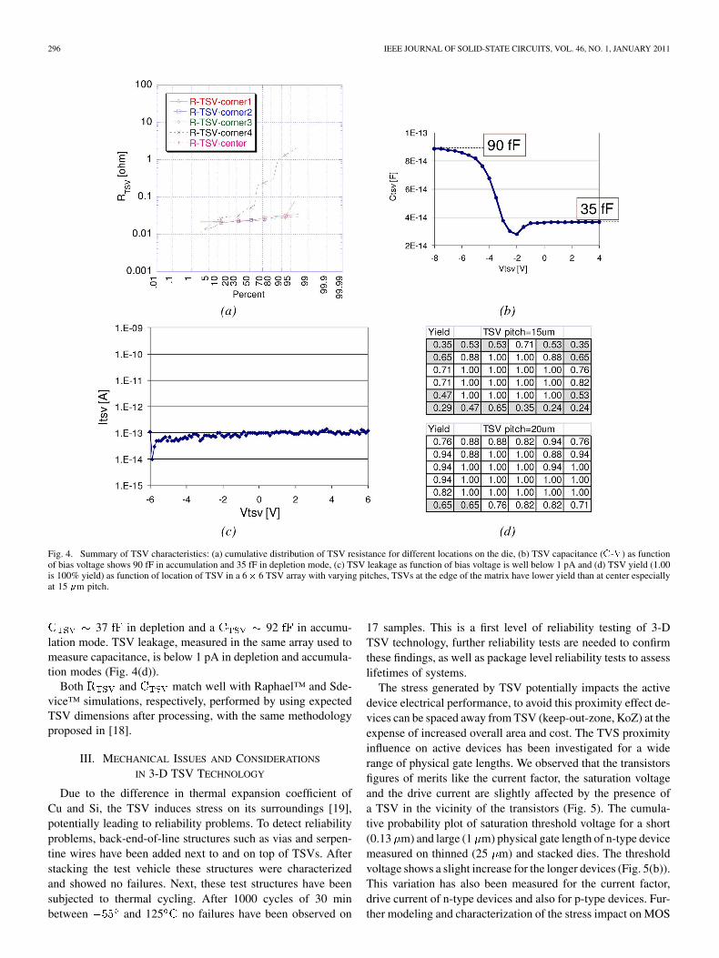
DC Resistance and low frequency capacitance are fun-damental electrical parameters of TSVs. Measure of TSVresistance between the top of the TSV and the landing padprovides information on the quality of the vertical electricalconnection established by the bonding of the staked dies. Withthe proposed TSV dimensions, TSV resistance is expectedto be in the order of few tens of milliohms in good TSVs.Therefore, the resistance test structure consists of a singleTSV in a 4-point or Kelvin configuration. The Kelvin TSV isplaced the four corners and in the center of each stacked die.The measured values show 20 m ; the spread overdifferent die locations and over 17 dies is limited (Fig. 4(a)),thus indicating a good quality of 3-D stacking and bonding.
Dense clusters of TSVs, consisting of arrays of 6 6 TSVwhere each TSV is measured in a 2 point configuration for as-sessing the 3-D connectivity only, show an evident pitch depen-dency of the TSV yield. In particular, TSVs in the array pe-riphery do not provide good electrical connections at 15 mpitch. On the other hand, overall good yield is obtained for20 m pitch Fig. 4(c).
TSV capacitance is an essential parameter for 3-D circuitdesign. Since the TSV forms a cylindrical MIS (Metal-Insu-lator-Semiconductor) capacitor with the substrate, it is expectedthat this capacitance is non-linear and depends on the biasing ofthe TSV with respect to the substrate. TSV capacitance valuesare expected to be in the order of 100 . These are too lowfor the accuracy of a standard LCR meter; therefore, arrays of32 TSVs connected in parallel are used to measure a larger valueof capacitance, which is then averaged over the number of TSVsin the parallel array. De-embedding structures are also charac-terized to reduce the impact of parasitics on the measurements.
- plots of TSV capacitance @ 1 MHz (Fig. 4(b)), show a
296 IEEE JOURNAL OF SOLID-STATE CIRCUITS, VOL. 46, NO. 1, JANUARY 2011
Fig. 4. Summary of TSV characteristics: (a) cumulative distribution of TSV resistance for different locations on the die, (b) TSV capacitance ( - ) as functionof bias voltage shows 90 fF in accumulation and 35 fF in depletion mode, (c) TSV leakage as function of bias voltage is well below 1 pA and (d) TSV yield (1.00is 100% yield) as function of location of TSV in a 6 6 TSV array with varying pitches, TSVs at the edge of the matrix have lower yield than at center especiallyat 15 m pitch.
37 in depletion and a 92 in accumu-lation mode. TSV leakage, measured in the same array used tomeasure capacitance, is below 1 pA in depletion and accumula-tion modes (Fig. 4(d)).
Both and match well with Raphael™ and Sde-vice™ simulations, respectively, performed by using expectedTSV dimensions after processing, with the same methodologyproposed in [18].
III. MECHANICAL ISSUES AND CONSIDERATIONS
IN 3-D TSV TECHNOLOGY
Due to the difference in thermal expansion coefficient ofCu and Si, the TSV induces stress on its surroundings [19],potentially leading to reliability problems. To detect reliabilityproblems, back-end-of-line structures such as vias and serpen-tine wires have been added next to and on top of TSVs. Afterstacking the test vehicle these structures were characterizedand showed no failures. Next, these test structures have beensubjected to thermal cycling. After 1000 cycles of 30 minbetween and 125 no failures have been observed on
17 samples. This is a first level of reliability testing of 3-DTSV technology, further reliability tests are needed to confirmthese findings, as well as package level reliability tests to assesslifetimes of systems.
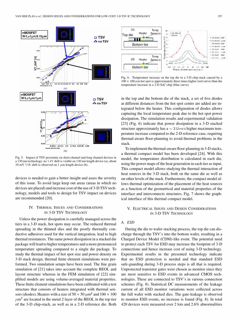
The stress generated by TSV potentially impacts the activedevice electrical performance, to avoid this proximity effect de-vices can be spaced away from TSV (keep-out-zone, KoZ) at theexpense of increased overall area and cost. The TVS proximityinfluence on active devices has been investigated for a widerange of physical gate lengths. We observed that the transistorsfigures of merits like the current factor, the saturation voltageand the drive current are slightly affected by the presence ofa TSV in the vicinity of the transistors (Fig. 5). The cumula-tive probability plot of saturation threshold voltage for a short(0.13 m) and large (1 m) physical gate length of n-type devicemeasured on thinned (25 m) and stacked dies. The thresholdvoltage shows a slight increase for the longer devices (Fig. 5(b)).This variation has also been measured for the current factor,drive current of n-type devices and also for p-type devices. Fur-ther modeling and characterization of the stress impact on MOS
VAN DER PLAS et al.: DESIGN ISSUES AND CONSIDERATIONS FOR LOW-COST 3-D TSV IC TECHNOLOGY 297
Fig. 5. Impact of TSV proximity on short channel and long channel devices ina 130 nm technology: no shift is visible on 130 nm length device (a), about10 mV shift is observed on 1 m length device (b).
devices is needed to gain a better insight and asses the severityof this issue. To avoid large keep out areas (areas in which nodevices are placed) and increase cost of the use of 3-D TSV tech-nology, models and tools to design for TSV impact on devicesare recommended [20].
IV. THERMAL ISSUES AND CONSIDERATIONS
IN 3-D TSV TECHNOLOGY
Unless the power dissipation is carefully managed across thetiers in a 3-D stack, hot spots may occur. The reduced thermalspreading in the thinned dies and the poorly thermally con-ductive adhesives used for the vertical integration, lead to highthermal resistances. The same power dissipation in a stacked diepackage will lead to higher temperatures and a more pronouncedtemperature spreading compared to a single die package. Tostudy the thermal impact of hot spot size and power density on3-D stack design, thermal finite element simulations were per-formed. Two simulation setups have been used. The fine grainsimulation of [21] takes into account the complete BEOL andlayout structure whereas in the FEM simulation of [22] sim-plified models are using volume-averaged material properties.These finite element simulations have been calibrated with a teststructure that consists of heaters integrated with thermal sen-sors (diodes). Heaters with a size of 50 50 m and 100 100
m are located in the metal 2 layer of the BEOL in the top tierof the 3-D chip-stack, as well as in a 2-D reference die. Both
Fig. 6. Temperature increase on the top die in a 3-D chip-stack caused by a100 100 m hot spot is approximately three times higher (red curve) than thetemperature increase in a 2-D SoC chip (blue curve).
in the top and the bottom die of the stack, a set of five diodesat different distances from the hot spot centre are added are in-tegrated below the heater. This configuration of diodes allowscapturing the local temperature peak due to the hot spot powerdissipation. The simulation results and experimental validation[23] (Fig. 6) indicate that power dissipation in a 3-D stackedstructure approximately has a higher maximum tem-perature increase compared to the 2-D reference case, requiringthermal-aware floor-planning to avoid thermal problems in thestack.
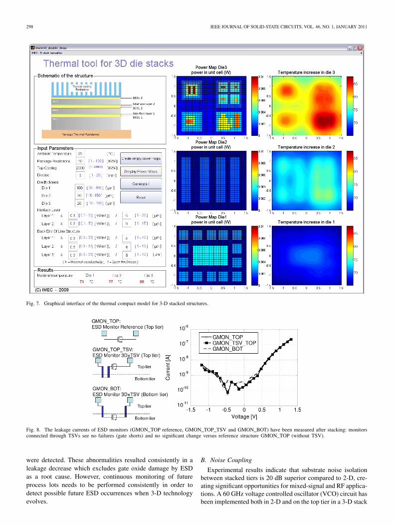
To implement the thermal-aware floor-planning in 3-D stacks,a thermal compact model has been developed [24]. With thismodel, the temperature distribution is calculated in each die,using the power maps of the heat generation in each tier as input.This compact model allows studying the thermal interaction ofheat sources in the 3-D stack, both on the same die as well ason other levels of the stack. Furthermore, the compact model al-lows thermal optimization of the placement of the heat sourcesas a function of the geometrical and material properties of theinterface and interconnects structures. Fig. 7 shows the graph-ical interface of this thermal compact model.
V. ELECTRICAL ISSUES AND DESIGN CONSIDERATIONS
IN 3-D TSV TECHNOLOGY
A. ESD
During the die to wafer stacking process, the top die can dis-charge through the TSV’s into the bottom wafer, resulting in aCharged Device Model (CDM)-like event. The potential needto protect each TSV for ESD may increase the footprint of 3-Dconnections and hence increase cost of using 3-D technology.Experimental results in the presented technology indicatethat no ESD protection is needed and that standard ESDsafe-guarding during 3-D process steps is all that is required.Unprotected transistor gates were chosen as monitor since theyare most sensitive to ESD events in advanced CMOS tech-nologies. These are connected to TSV’s in various connectionschemes (Fig. 8). Statistical DC measurements of the leakagecurrent of all ESD monitor variations were collected acrossthe full wafer with stacked dies. The gate-leakage is observedto monitor ESD events, no increase is found (Fig. 8). In total420 devices were measured over 2 lots and 2.6% abnormalities
298 IEEE JOURNAL OF SOLID-STATE CIRCUITS, VOL. 46, NO. 1, JANUARY 2011
Fig. 7. Graphical interface of the thermal compact model for 3-D stacked structures.
Fig. 8. The leakage currents of ESD monitors (GMON_TOP reference, GMON_TOP_TSV and GMON_BOT) have been measured after stacking: monitorsconnected through TSVs see no failures (gate shorts) and no significant change versus reference structure GMON_TOP (without TSV).
were detected. These abnormalities resulted consistently in aleakage decrease which excludes gate oxide damage by ESDas a root cause. However, continuous monitoring of futureprocess lots needs to be performed consistently in order todetect possible future ESD occurrences when 3-D technologyevolves.
B. Noise Coupling
Experimental results indicate that substrate noise isolationbetween stacked tiers is 20 dB superior compared to 2-D, cre-ating significant opportunities for mixed-signal and RF applica-tions. A 60 GHz voltage controlled oscillator (VCO) circuit hasbeen implemented both in 2-D and on the top tier in a 3-D stack

VAN DER PLAS et al.: DESIGN ISSUES AND CONSIDERATIONS FOR LOW-COST 3-D TSV IC TECHNOLOGY 299
Fig. 9. 2-D SoC and 3-D chip-stack mmWave VCO implementation andschematic: 20 dB reduction of noise coupling in 3-D versus 2-D is observed.
(Fig. 9) to verify the isolation of 3-D versus 2-D. The VCO per-formance (center frequency, phase noise) is unaffected by thestacking operation. Both on the 2-D chip and the bottom tier ofthe 3-D stack a controlled “substrate noise” signal is injected tomeasure noise coupling as in [25]. This substrate noise signalemulates the switching activity of a digital circuit. The emu-lating waveform is a sine-wave with a frequency that is variedfrom 1 MHz to 1 GHz, which in practice extracts the coupling inthe frequency domain. Due to coupling into the VCO the noisesignal appears as unwanted spurs at the output of the VCO atan offset equal to its frequency. The level of the spur power is ameasure for the noise coupling, or in other words a lower spurpower shows that the isolation is better. The 3-D version ex-hibits a 20 dB lower level of spur power than the 2-D SoC variantthroughout the frequency range of noise from 1 MHz to 30 MHzbeyond which the 3-D spur level drops below noise. This indi-cates isolation is 20 dB better in the lower frequency range upto 30 MHz and noise of 2-D-SoC variant exceeds noise in 3-Dup to 300 MHz (Fig. 9). This improved isolation capability of3-D technology opens up opportunities for high performancemixed-signal system design.
C. Transmitting Digital Signals Through TSVs
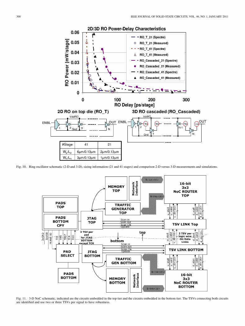
Ring Oscillator (RO) is a standard digital circuit to analyzea particular technology and it is used to verify the feasibility of3-D circuits and the impact of TSV on digital signaling and cir-cuit operation. 2-D and 3-D RO circuits with varying number ofstages and inverter sizes are compared. 21 and 41-stage 3-D ringoscillators with 1 TSV/stage and without TSVs are implementedas shown in Fig. 10. All RO configurations have their outputconnected to 8 stage frequency divider (divide by 256) to enablereliable frequency measurements (0.1–200 MHz). To predict theperformance of a 3-D circuit, calibrated device models for thetransistors along with lumped “T” RC model of the TSV [18]with measured and values are used. Simulation re-sults of power-delay characteristics of the functional RO imple-mentation are well in agreement with measurements suggestingthat the model with extracted values can also be extended for
predicting the performance of more complex 3-D circuits. It canbe also seen that because of smaller inverter sizes the delay ex-hibited by 21 stage 3-D RO is larger when compared to the delaycaused by 41 stage 3-D RO. Hence, in real circuit applications,strong driver elements are necessary to limit the delay causedby TSV in 3-D circuits.
VI. 3-D NETWORK ON CHIP DEMONSTRATOR CIRCUIT
The communication architectures of choice in today’sstate-of-the-art designs are structured and scalable Net-works-on-Chip [26], [27]. The extension of the NoC paradigmto 3-D integrated circuits is very promising, as modularity andscalability are even more critical for future three-dimensionalintegrated systems [28].
To demonstrate the feasibility of this communication ar-chitecture, we designed and manufactured a 16-bit 3-D NoCdistributed across two tiers using the iNoCs synthesizableNoC IP and tool chain, with extensions for supporting verticallinks (Fig. 11). Each tier consists of a traffic generator, a slavememory, a 3 3 switch and a JTAG controller. The trafficgenerators mimic logic IP components and can send/receivedata packets at NoC speed to and from the memory on eachtier. A JTAG controller is inserted on each tier to supportKnown-Good-Die testing before stacking. It also supportstesting of the 3-D link after stacking. Note that the test pads ofthe bottom tier are no longer accessible after stacking. There-fore, these are replicated on the top tier. The PAD SELECTMUX connects these replicated pads to the JTAG bottom blockif the top die is present.
A 2.5D design approach was followed to layout the 3-D NOC,i.e., each tier was independently designed but for the TSVs ofwhich the position was aligned on both tiers during P&R. Intotal 100 TSVs are used to interconnect both tiers: 12 for 2 6for VDD/GND, 2 (2 16) for the 3-D link, 3 8 for the test.Both tiers are manufactured in a the 200 mm/130 nm FEOLCMOS technology with Cu/SiO2 BEOL and 3-D Cu TSV asdescribed in Section I.A. The die-to-wafer configuration allowsthe selection of KGD prior to stacking, reducing cost of the 3-Dprocessing.
The NoC switches in each tier are connected through a TSVlink. Each signal line across the 3-D link is implemented witha standard CMOS buffer (BUFBD2) attached to two TSVs(Fig. 12). TSV duplication per signal is used to protect the linkagainst TSV opens, which is the most frequently occurringfault in our process technology (as described in Section II.B).No ESD protection is used on the 3-D link, as our experimentalresults indicate that sufficient safe-guarding during 3-D processsteps is all that is required (Section V.A).
When activating the NoC, we first enable KGD die testingby ensuring that each 3-D input signal on each tier is drivento a logic value. To this end, we have attached a weak pulldown diode to each TSV. The leakage current of the diode ininversion ensures that the input signal of the receiving tier (theTSV_SLECT_MUX) is not floating. Second, we have added theTSV_SLECT_MUX to collect statistics on TSV yield. With thisMUX each TSV can be individually tested at boot time through
300 IEEE JOURNAL OF SOLID-STATE CIRCUITS, VOL. 46, NO. 1, JANUARY 2011
Fig. 10. Ring oscillator schematic (2-D and 3-D), sizing information (21 and 41 stages) and comparison 2-D versus 3-D measurements and simulations.
Fig. 11. 3-D NoC schematic, indicated are the circuits embedded in the top tier and the circuits embedded in the bottom tier. The TSVs connecting both circuitsare identified and use two or three TSVs per signal to have robustness.

VAN DER PLAS et al.: DESIGN ISSUES AND CONSIDERATIONS FOR LOW-COST 3-D TSV IC TECHNOLOGY 301
Fig. 12. TSVs for data links are tested using a scan chain and multiplexer. After testing the TSV that functions correctly is selected.
the scan-chain. A test pattern is injected into the scan registersand applied by setting the DATA_SLCT_MUX. After transmit-ting the data, the receiving register is sampled and scanned inorder to detect faulty TSVs. Based on simulation, the redun-dant TSV and TSV_SLECT_MUX increase the 3-D link delayby 1.6 , and its power consumption by 1.8 with respect to asingle CMOS buffer (BUFBD2) driving a single TSV. In case ofa TSV process technology where TSV shorts to bulk frequentlyoccur, the above TSV IO scheme can be adapted by replacingthe buffer driving both TSVs with a DEMUX, controlled by ad-ditional configuration memories. The DEMUX can then discon-nect the failing TSVs from the buffers driving them.
The 3-D NoC operation is depicted in Fig. 13(a). After poweron, the design is switched in test mode. First, we program which32 TSVs out of the total 64 are used for transmitting data onthe data link (step 1). Second, we configure what data patternstraffic generators should transmit (step 2). Thereafter, the NoCis switched in operation mode (step 3). In the depicted test-case, short bursts of 32-bits are transmitted in 96-bit networkpackets. The packets are respectively sent in 3-D across the TSVlinks from the top(bottom) traffic generator to the bottom(top)memory or in 2-D from the bottom(top) traffic generator to thebottom(top) memory. Finally, the data is scanned out again. Theoutput (tdo) corresponds with the expected output (tdo_exp),confirming a successful operation of the 3-D NoC. Separately,we have tested the 3-D link by transmitted alternating patternsof 0–1/1–0 transitions across the TSV link. So far, we have notfound failing TSV on the 3-D NoC link (Fig. 13(b)).
The additional area penalty for the TSVs in the 3-D stackis limited to 0.018 mm (Fig. 14). We have placed the TSVinterconnect in a regular array of two columns with a pitch of13 m next to the standard cell core area to optimize yield.In this way we avoided TSV proximity impact as discussed inSection III, at the expense of slightly increased overall area.The power penalty for 3-D data transfers is only 3% withrespect to sending the same continuous stream of 32-bit databursts in 2-D, between memory and traffic generator spaced atless than 0.5 mm on the same tier. For 3-D communication at50 MHz supply 1.39 mW is consumed from a 1.2 V comparedto 1.34 mW for 2-D. The delay of the 3-D link is 183 ps,enabling high speed data transfers. The 3-D interconnects inthe NoC can be designed to operate at a much higher speed.Characterization of ring oscillators driving TSVs shows thatdata can be transferred across a TSV in less than 150 ps whileconsuming less than 2 pJ/bit energy at 1.2 V (Section V.C).TSVs thus enable transferring of data between dies at a similarspeed than intra-die data.
In this section, we have demonstrated a testable 3-D NoCmanufactured using a low cost 3-D TSV Stacked-IC technology.This result indicates that modular integration of scalable sys-tems with IP components distributed across multiple dies isfeasible.
VII. SUMMARY AND CONCLUSIONS
In this paper key design issues and considerations of alow-cost 3-D Cu-TSV technology have been investigated.

302 IEEE JOURNAL OF SOLID-STATE CIRCUITS, VOL. 46, NO. 1, JANUARY 2011
Fig. 13. Output of scope during wafer-level test; (a) transmission of data burst across TSV links. The expected output (tdo) matches with logic simulation (tdo_exp).Measured maximum performance (25 [email protected]–1.5 V) is limited by wafer-level test setup; (b) JTAG test results of TSVs in d_link (from bottom to top tier); all38 TSVs in this link are functionally working.
Fig. 14. Microchip photograph of the top tier of the 3-D NoC, indicated arethe area consumed by the TSV array ( 2 ), cell NoC core including drivers( 87 ) and I/O area ( 11 ) of the total 1 1 mm block.
Thermal cycling while carefully monitoring the integrity ofBEOL around TSVs has shown 3-D does not compromise re-
liability of BEOL. The impact of TSV stress on MOS devicescauses shifts, to account for this during design furtheranalysis and modeling is advised. Thermal hot spots in 3-Dchip stacks cause temperature increases three times higherthan in 2-D chips, we have proposed thermal floorplanning totake this into account during design. We have found no ESDevents during 3-D processing, however careful further moni-toring is required. The noise coupling between two tiers in a3-D chip-stack is 20 dB lower than in a 2-D SoC, openingopportunities for increased mixed signal system performance.The impact on digital circuit performance of TSVs is accu-rately modeled with the proposed RC model and ring oscilla-tors spanning both tiers in the stack show that digital signalscan be driven through TSVs at high speed and low power.Experimental results of a 3-D Network-on-Chip implementa-tion demonstrate that the NoC concept can be extended from2-D to 3-D SoCs at low area (0.018 mm ) and power (3%)overhead.

VAN DER PLAS et al.: DESIGN ISSUES AND CONSIDERATIONS FOR LOW-COST 3-D TSV IC TECHNOLOGY 303
REFERENCES
[1] S. Gu et al., “Stackable memory of 3-D chip integration for mobileapplications,” in Proc. IEDM ’08, pp. 1–4.
[2] U. Kang et al., “8 Gb 3-D DDR3 DRAM using through-silicon-viatechnology,” in Proc. ISSCC 09, pp. 130–131, 07.2.
[3] H. Yoshikawa et al., “Chip-scale camera module (CSCM) usingthrough-silicon-via (TSV),” in Proc. ISSCC 09, pp. 476–477, 28.5.
[4] Y. Suntharalingam et al., “A 4-side tileable back-illuminated 3-D-in-tegrated mpixel CMOS image sensor,” in Proc. ISSCC 09, 02.1.
[5] K. Ishida et al., “A 1.8 V 30 nJ adaptive program-voltage (20 V) gen-erator for 3-D-integrated NAND flash SSD,” in Proc. ISSCC 09, pp.38–39, 13.5.
[6] J. Van Olmen et al., “3-D stacked IC demonstration using a throughsilicon via first approach,” in Proc. IEDM, 2008, pp. 303–306.
[7] M. Koyanagi, T. Nakamura, Y. Yamada, H. Kikuchi, T. Fukushima,T. Tanaka, and H. Kurino, “Three-dimensional integration technologybased on wafer bonding with vertical buried interconnections,” IEEETrans. Electron Devices, vol. 53, no. 11, pp. 2799–2808, Nov. 2006.
[8] P. S. Andry, C. K. Tsang, E. Sprogis, C. Patel, S. L. Wright, B. C.Webb, L. P. Buchwalter, D. Manzer, R. Horton, R. Polastre, and J. U.Knickerbocker, “A CMOS compatible process for fabricating electricalthrough vias in silicon,” in Proc. 56th Electronic Components Technol.Conf., San Diego, CA, 2006, pp. 831–837.
[9] E. Beyne et al., “Through-silicon via and die stacking technologies formicrosystems-integration,” in Proc. IEDM, 2008, pp. 1–4.
[10] S. Gupta, M. Hilbert, S. Hong, and R. Patti, “Techniques for producing3-D ICs with high-density interconnect,” in Proc. VLSI Multi-Level In-terconnection Conf., 2004, pp. 56–59.
[11] J. Burns, L. McIlrath, C. Keast, C. Lewis, A. Loomis, K. Warner, andP. Wyatt, “Three-dimensional integrated circuits for low-power, high-bandwidth systems on a chip,” in Proc. Papers IEEE Int. Solid-StateCircuits Conf. Tech. Dig., 2001, pp. 268–269.
[12] R. Chatterjeea et al., “Three-dimensional integrated circuits for low-power, highbandwidth systems on a chip,” in Proc. IEEE Int. Intercon-nect Technol. Conf., 2007, pp. 81–83.
[13] J. A. Burns, B. F. Aull, C. K. Chen, C.-L. Chen, C. L. Keast, J. M.Knecht, V. Suntharalingam, K. Warner, P. W. Wyatt, and D.-R. W.Yost, “A wafer-scale 3-D circuit integration technology,” IEEE Trans.Electron Devices, vol. 53, no. 10, pp. 2507–2516, Oct. 2006.
[14] T. Mitsuhashi et al., “Development of 3-D-packaging process tech-nology for stacked memory chips,” in Proc. Enabling Technologies for3-D Integration Symp., Boston, MA, Nov. 27–29, 2006, pp. 155–62.
[15] D. Henry et al., “Through silicon vias technology for CMOS imagesensors packaging: Presentation of technology and electrical results,”in Proc. EPTC 2008, Singapore, Dec. 9–12, 2008, pp. 35–44.
[16] G. Van der Plas et al., “Design issues and solutions for low-cost 3-DTSV IC technology,” in Proc. ISSCC 10, pp. 148–149, 07.8.
[17] A. Jourdain et al., “Electrically yielding collective hybrid bonding for3-D stacking of ICs,” in Proc. ECTC, 2009, pp. 11–13.
[18] G. Katti et al., “Electrical modeling and characterization of throughsilicon via for three-dimensional ICs,” IEEE Trans. Electron Devices,vol. 57, no. 1, pp. 256–262, Jan. 2010.
[19] C. Okoro et al., “Extraction of the appropriate material property for re-alistic modeling of through-silicon-vias using -Raman spectroscopy,”in Proc. IITC 08, pp. 16–18.
[20] R. Radojcic et al., “Design for manufacturability for fabless manufac-turers,” IEEE Solid-State Circuits Mag., vol. 1, no. 3, pp. 25–33, Mar.2009.
[21] H. Oprins et al., “Fine grain thermal modeling of 3-D stacked struc-tures,” in Proc. THERMINIC, 2009, pp. 45–49.
[22] C. Torregiani et al., “Thermal analysis of hot spots in advanced 3-D-stacked structures,” in Proc. THERMINIC, 2009, pp. 56–60.
[23] H. Oprins et al., “Fine grain thermal modeling and experimental vali-dation of 3-D-ICs,” Microelectronics J., Nov. 2009, submitted for pub-lication.
[24] C. Torregiani et al., “A wafer-scale 3-D circuit integration technology,”in Proc. EPTC, 2009, pp. 131–136.
[25] C. Soens, G. Van der Plas, P. Wambacq, S. Donnay, and M. Kuijk, “Per-formance degradation of LC-tank VCOs by impact of digital switchingnoise in lightly doped substrates,” IEEE J. Solid-State Electron., vol.40, no. 7, pp. 1472–1481, Jul. 2005.
[26] S. Vangal et al., “An 80-Tile 1.28 TFLOPS network-on-chip in 65 nmCMOS,” in Proc. ISSCC, 2007, pp. 98–99.
[27] K. Kim et al., “A 125 GOPS 583 mW network-on-chip based parallelprocessor with bio-inspired visual attention engine,” in Proc. ISSCC08, p. 308.
[28] I. Loi et al., “A low-overhead fault tolerance scheme for TSV-based3-D network on chip links,” in Proc. ICCAD 08, pp. 598–602.
Geert Van der Plas (M’03) received the M.Sc.and Ph.D. degrees from the Katholieke UniversiteitLeuven, Belgium, in 1992 and 2001, respectively.
From 1992 to 2002, he was a Research Assistantwith ESAT-MICAS of the Katholieke UniversiteitLeuven. He joined imec (SSET), Belgium, in 2003,where he is a principal scientist. He has been workingon energy efficient data converters, low-power scal-able radios, power and signal integrity and designtechnology for 3-D integration. He has authoredand co-authored over 100 papers in journals and
conference proceedings and serves on the technical program committee of theSymposium on VLSI Circuits.
Paresh Limaye received the B.S. degree from Uni-versity of Pune, India, in 1998, the M.S. degree fromthe State University of New York at Binghamtonin 2000, and the Ph.D. degree from KatholiekeUniversiteit Leuven, Belgium, all in mechanicalengineering.
He is currently working at the Interuniversity Mi-croElectronics Center (IMEC), Leuven, Belgium, inthe field of 3-D IC stacking and packaging. His mainfields of interest and experience include electronicspackaging, electronics assembly and manufacturing,
finite element analysis, reliability and failure analysis. He has worked in thefield of flip chip and SiP packaging at Amkor Technology, Chandler, AZ, andTemex Microsonics, Sophia Antipolis, France.
Igor Loi received the B.S. degree in electrical en-gineering from the University of Cagliari, Cagliari,Italy, in 2005 and the Ph.D. degree in the Departmentof Electronics and Computer Science, University ofBologna, Italy, in 2010.
He is currently holding the position of post-doc inelectronic engineering at the University of Bologna.He is focusing his research on three-dimensional in-tegrated circuit technologies and Networks-on-Chip.
Abdelkarim Mercha received the M.Sc. degreein electrical engineering from the Ecole NationaleSupérieure d’Ingénieurs de Caen (ENSI de Caen),Caen, France, and the Ph.D. degree in microelec-tronics from the University of Caen, Caen, France,in 1997 and 2000, respectively.
In 2001, he joined the Interuniversity MicroElec-tronics Center (IMEC), Leuven, Belgium, His inter-ests cover the fields of Analog RF, Logic and Memorydevices, 3-D Stacked ICs integration. In these fields,he has (co-)authored over 250 journal and conference
papers and two book chapters. He is the editor for the journals Fluctuation andNoise Letters and Active and Passive Electronic Components.
304 IEEE JOURNAL OF SOLID-STATE CIRCUITS, VOL. 46, NO. 1, JANUARY 2011
Herman Oprins received the M.Sc. degree inmechanical engineering from the Katholieke Uni-versiteit Leuven, Belgium, in 2003. In 2010, hereceived the Ph.D. degree from the same universityin collaboration with imec on the modeling anddevelopment of an electrowetting based coolingtechnique for electronic components.
Since 2009, he has been with imec working onthermal management of electronic systems. Hisresearch interests include thermal characterizationof 3-D integration, thermal modeling, microfluidics
and electrowetting.
Cristina Torregiani received the M.Sc degree inphysics from the University of Bari, Bari, Italy, in2001, where she also worked from 1999 to 2001on the development of thin films photocathodes.She received the Ph.D. degree on process-inducedstress and strain in planar transistors from theESAT-INSYS division of the Katholieke UniversiteitLeuven, Belgium.
In 2002 she was involved in a research projectwith IMEC on ultra-shallow-junctions anneal foradvanced CMOS applications. In 2007 she joined
the Packaging Reliability division of Interuniversity MicroElectronics Center(IMEC), Leuven, Belgium, where she worked on thermal and thermo-mechan-ical modeling and characterization of packaging for microelectronics. In 2010she joined Qualcomm, where she overviews the Imec-Qualcomm joint programon 3-D integration as resident in Imec.
Steven Thijs (M’08) received the M.Sc. and Ph.D.degrees in electrotechnical engineering from theKatholieke Universiteit Leuven (KUL) Belgium, in2001 and 2009 respectively.
He joined the Silicon Processing and Device Re-liability group of Interuniversity MicroElectronicsCenter (IMEC), Leuven, Belgium, in 2001, wherehe was involved in ESD protection design, layout,simulation and characterization on CMOS andBiCMOS technologies and in RF circuit design withESD protection. In 2006, he started working towards
a Ph.D. in the field of ESD protection for FinFET devices and for RF CMOScircuits. He has authored and co-authored over 100 publications in the field.
Dr. Thijs received the Best Paper and Best Student Paper Award from theEOS/ESD Symposium in 2004 and 2008 respectively. He served as a memberof the Technical Program Committee of the EOS/ESD Symposia 2007–2010and IRPS 2009. He is a member of IEEE and a peer reviewer for various IEEEjournals.
Dimitri Linten (S’01–M’06) received the M.Sc.and Ph.D. degrees in electrical engineering fromthe Vrije Universiteit Brussel (VUB), Brussels,Belgium, in 2001 and 2006, respectively.
In 2001, he joined the Wireless Research groupof Interuniversity MicroElectronics Center (IMEC),Leuven, Belgium In 2006, he joined the depart-ment Fundamental Electricity and Instrumentation(ELEC) at the Vrije Universiteit Brussel and the ESDreliability group at IMEC as a post-doctoral researchfellow, supported by the Institute for the Promotion
of Innovation through Science and Technology in Flanders (IWT-Vlaanderen).In 2007, he became the scientific coordinator of the ESD research group atIMEC. His research interests are on-wafer ESD testers, ESD-reliable RF circuitdesign and ESD reliability for sub-32 nm finfet and planar devices, high voltagesilicon technologies, Radiation and Python OOP. He authored or co-authoredmore then 100 publications and patents in these fields.
Dr. Linten received the Best Paper Award from the EOS/ESD Symposium2004. In 2010, he co-founded an Open Source Initiative on ESD data analysisSoftware He is serving in the TPC of ESREF, ICICDT and IEW. He is a memberof Management Committee of the International ESD Workshop 2011 (IEW).
Michele Stucchi received the M.S. degree in elec-trical engineering from the University of Bari, Italy,in 1988.
From 1989 to 1991 he worked as interconnect andsilicide process engineer for DRAM plant of TexasInstruments, Avezzano, Italy, and from 1991 to 1996as an engineer in failure analysis, FIB analysis andin ESD and latch-up characterization of IC devicesin Tecnopolis science park, Bari, Italy. In 1996he joined Interuniversity MicroElectronics Center(IMEC), Leuven, Belgium, where he managed the
Technology-Aware Design research program. He currently works as SeniorResearch Engineer in characterization, modeling and reliability aspects of 2-Dand 3-D interconnects.
Guruprasad Katti received the B.E. degree inelectrical engineering from A.C. Patil College ofEngineering, University of Mumbai, Mumbai, India,and the M.S. degree in electrical engineering fromthe Indian Institute of Technology Madras, Chennai,India, in 1999 and 2002, respectively. He is cur-rently pursuing the Ph.D. degree in InteruniversityMicroElectronics Center (IMEC), Leuven, Belgium,and Katholieke Universiteit Leuven (KUL) on 3-DIC interconnects.
Prior to joining the Ph.D. program he worked withGE-Global Research and National Semiconductor, Bangalore, India.
Mr. Katti is a recipient of the IEEE EDS Ph.D. Student Fellowship Awardfor the year 2010. His research interests include 3-D ICs, IC interconnects andnovel device structures.
Dimitrios Velenis received the M.Sc. and Ph.D. de-grees from the University of Rochester, Rochester,NY, in 2000 and 2003, respectively.
He was an Assistant Professor with the Departmentof Electrical and Computer Engineering, Illinois In-stitute of Technology, until Fall 2007 and a ResearchAssociate at the University of Rochester until Spring2008. Since April 2008 he has been with Interuniver-sity MicroElectronics Center (IMEC), Leuven, Bel-gium, working on characterization and cost modelingof 3-D integration processing. He has been the author
or coauthor of over 30 papers in journals and conference proceedings.Dr. Velenis was the recipient of the 2004 Outstanding Dissertation Award
from the European Design Automation Association.
Vladimir Cherman received the M.Sc. and Ph.D.degrees in electronic engineering from Saint Pe-tersburg Electrotechnical University (ETU-LETI),Russia, in 1994 and 1999, respectively.
From 1997 to 2000, he was with Morion Inc.,Saint Petersburg, Russia, as an electronics engineer.From 2000 to 2007 he was with Ceramics Lab-oratory at Swiss Federal Institute of TechnologyLausanne (EPFL) where his research was focusedon microwave properties of ferroelectric materials.He joined the Reliability and Modeling group of
Interuniversity MicroElectronics Center (IMEC), Leuven, Belgium, as aResearcher in 2007, where he is involved in reliability study of MEMS devicesand electronic packages.

VAN DER PLAS et al.: DESIGN ISSUES AND CONSIDERATIONS FOR LOW-COST 3-D TSV IC TECHNOLOGY 305
Bart Vandevelde received the M.S. degree in me-chanical engineering from the Catholic University ofLeuven, Belgium, in June 1994. In March 2002, hereceived the Ph.D. degree at Interuniversity Micro-Electronics Center (IMEC), Leuven, Belgium, in thefield of thermo-mechanical modeling for electronicsystems.
Currently, he is team leader for the packaging reli-ability activities at IMEC and internal project coordi-nator for several Flemish and European projects. Heis co-founder and member of the organization com-
mittee for the Eurosime conference.
Veerle Simons is currently working in the reliabilitygroup (INTPAC/REMO) of the Process Technologyunit at Interuniversity MicroElectronics Center(IMEC), Leuven, Belgium.
Ingrid De Wolf (SM’07) has been with Interuniver-sity MicroElectronics Center (IMEC), Leuven, Bel-gium since 1989.
She performed research on reliability physics ofsemiconductor devices, with special attention formechanical stress aspects and failure analysis. Since1999, she heads the group REMO (Reliability andModelling), where research is focused on test andreliability of MEMS and IC-interconnect and pack-aging, including 3-D. She is a part time Professorin the Metals and Applied Materials Engineering
Department of the Katholieke Universiteit Leuven, Belgium.
Riet Labie received the M.Sc. and Ph.D. degrees inmaterials science from the Katholieke UniversiteitLeuven, Belgium, in 1999 and 2007, respectively.
She joined Interuniversity MicroElectronicsCenter (IMEC), Leuven, Belgium, in 1999, whereshe first worked as Process and Research Engineerin packaging and flip chip interconnections. In 2008,she started working as a reliability engineer forpackaging and interconnects, with particular focuson 3-D.
Dan Perry received the B.S.E.E. degree from theUniversity of California at San Diego.
He is a Staff Engineer at Qualcomm workingon 3-D integration issues. He recently completeda two year assignment at Interuniversity Micro-Electronics Center (IMEC), Leuven, Belgium.His previous assignments at Qualcomm includeevaluation of design-for-manufacturability tools anddesign enablement. Prior to joining Qualcomm, heheld engineering positions with PDF Solutions andCadence Design Systems.
Stephane Bronckers received the M.S. degree inengineering from the Vrije Universiteit Brussel(VUB), Belgium, in 2005, and the Ph.D. degree fromInteruniversity MicroElectronics Center (IMEC),Leuven, Belgium.
In 2006 he joined the Fundamental Electricity andInstrumentation (ELEC) Department at the VUB asa research assistant supported by the Institute for thePromotion of Innovation Through Science and Tech-nology in Flanders (IWT-Vlaanderen). He worked atthe Wireless Group of IMEC. His research focused on
developing a methodology to improve the electromagnetic immunity of analogintegrated RF circuits. In 2009, he joined the EMC Group of Laborelec, whichis part of the GDF-Suez group.
Nikolaos Minas received the M.Sc. and Ph.D. de-grees from Newcastle University, U.K.
Since 2008, he has been with imec (SSET), Bel-gium, where he is working as a researcher in the areaof 3-D Stacked Integrated Circuits (3-D-SIC).
Miro Cupac is currently working in the DigitalComponents Department (DC) of the Smart Systemsand Energy Technology unit at InteruniversityMicroElectronics Center (IMEC), Leuven, Belgium.
Wouter Ruythooren received the Ph.D. degree inmaterials engineering from Katholieke UniversiteitLeuven, Belgium, for a study on electrodepostion ofmagnetic materials in 2002.
He then initiated the development of GaN HEMTdevices at Interuniversity MicroElectronics Center(IMEC), Leuven, Belgium. In 2005, he took upresponsibility for advanced packaging activities, in-cluding development of TSV metallisation and metalbonding for 3-D stacking technology. Still at IMEC,in 2009, he became manager of all electroplating
activities. Since July 2010, he has been working in process development forsolar cells at Photovoltech, Belgium.
Jan Van Olmen is currently back-end of lineIntegration Engineer in the packaging group(INTPAC/PAMAHT) of the Process Technology unitat Interuniversity MicroElectronics Center (IMEC),Leuven, Belgium.

306 IEEE JOURNAL OF SOLID-STATE CIRCUITS, VOL. 46, NO. 1, JANUARY 2011
Alain Phommahaxay received the Ph.D. from theESYCOM-ESIEE, Noisy-le-Grand, France, in 2007.
Since 2007, he has been with InteruniversityMicroElectronics Center (IMEC), Leuven, Belgium,where he has been working in the litho group of theProcess Technology unit.
Muriel de Potter de ten Broeck received the M.S.degree in physics in 1978 and the Ph.D. degree in1984, both from the Katholieke Universiteit Leuvenin Leuven, Belgium.
From 1978 to 1984 she was a research assistantat the IKS (Instituut voor Kern-en Stralings Fysika)of the University of Leuven. In 1984 she joinedthe newly established R&D laboratory IMEC (In-teruniversity Micro-electronics Center) in Leuven,Belgium, as a member of the Compound Semicon-ductor Processing group. She has been working
on ion implantation in GaAs and on the development of advanced GaAsMESFET’s (microwave field-effect transistors). In 1995 she moved to theInterconnect Technologies and Silicides department within the Silicon ProcessTechnology Division. Since 2004 she is active, as a Senior Process Engineer,in the baseline process development for CMOS platform within the ProcessTechnology division.
Ann Opdebeeck is currently Process Assistant atInteruniversity MicroElectronics Center (IMEC),Leuven, Belgium.
From 2005 to 2006 she worked as a Customer As-sistant at NCI business center.
Michal Rakowski received the M.Sc. degree inelectronic engineering from the Warsaw Universityof Technology, Poland, in 2006.
Since 2006, he had been with the Institute ofMicroelectronics and Optoelectronics (VLSI En-gineering and Design Automation Division), at thesame university, working as a lecture assistant andpursing his Ph.D. From 2008 he has been with IMEC(Process Quality and Integration), Belgium, wherehe has been working on an electrical data analyzesand measurements.
Bart De Wachter is with Interuniversity MicroElec-tronics Center (IMEC), Leuven, Belgium, ProcessTechnology unit as a Researcher.
Morin Dehan received the B.S. and Ph.D. degreesin applied sciences from the Université Catholiquede Louvain, Louvain-la-Neuve, Belgium, in 1999 and2003, respectively.
Since 2004, he has been with Interuniversity Mi-croElectronics Center (IMEC), Leuven, Belgium. Heworked on modeling, and on the optimization of pas-sive components, fabricated in a CMOS process. Re-cently, he has been working on setting up PDKs forthe different imec technologies, for both 2-D and 3-Ddesigns.
Marc Nelis was born in Liège, Belgium. He receivedthe M.Sc. degree from the Université de Liege in2005.
From 2006 to 2007 he worked at NXP Semicon-ductors as Test & Product Engineer in the PowerManagement Unit. End of 2007 he joined Interuni-versity MicroElectronics Center (IMEC), Leuven,Belgium, (PQI) as Test Chip Engineer and is activein process test structures layout for new technologiesand data preparation for reticle.
Rahul Agarwal is currently Senior Research En-gineer at the Institute of Microelectronics (IME),Singapore.
From 2008 to 2010 he worked as researcher in 3-Dpackaging at Interuniversity MicroElectronics Center(IMEC), Leuven, Belgium, from 2001 to 2007 he wasResearch Assistant at University of South Florida.
Antonio Pullini received the M.S. degree in elec-trical engineering from Bologna University, Italy.
He is a Senior Engineer at iNoCs S.à.r.l., Lau-sanne, Switzerland. His research interests includelow-power digital design and networks on chip.
Federico Angiolini received the M.S. and Ph.D.degrees in electrical engineering from Bologna Uni-versity, Italy, on the subject of Networks-on-Chips.
He is the VP of Engineering at iNoCs S.à.r.l., Lau-sanne, Switzerland. His background is on architec-tural design and simulation environments.
VAN DER PLAS et al.: DESIGN ISSUES AND CONSIDERATIONS FOR LOW-COST 3-D TSV IC TECHNOLOGY 307
Luca Benini (F’07) is a Full Professor in the Depart-ment of Electronics and Computer Science, Univer-sity of Bologna.
He also holds a Visiting Professor position atEcole Federale Polytechnique de Lausanne. Hisresearch interests are in all the aspects of the com-puter-aided design of digital circuits, with specialemphasis on low-power applications, and in thedesign of portable systems. On these topics, hepublished more than 500 papers.
Wim Dehaene (SM’99) received the M.Sc. degreein electrical and mechanical engineering in 1991and the Ph.D. degree in 1996 from the KatholiekeUniversiteit Leuven, Belgium. His thesis is entitled“CMOS integrated circuits for analog signal pro-cessing in hard disk systems.”
After receiving the M.S. degree, he was a Re-search Assistant at the ESAT-MICAS Laboratoryof the Katholieke Universiteit Leuven. His researchinvolved the design of novel CMOS building blocksfor hard disk systems. The research was first spon-
sored by the IWONL (Belgian Institute for Science and Research in Industryand agriculture) and later by the IWT (the Flemish institute for Scientific Re-search in the Industry). In November 1996 he joined Alcatel Microelectronics,Belgium. There he was a senior project leader for the feasibility, design anddevelopment of mixed mode Systems on Chip. The application domains weretelephony, xDSL and high speed wireless LAN. In July 2002 he joined thestaff of the ESATMICAS laboratory of the Katholieke Universiteit Leuvenwhere he is now a Full Professor. His research domain is circuit level design ofdigital circuits. The current focus is on ultra low power signal processing andmemories in advanced CMOS technologies. Part of this research is performedin cooperation with IMEC, Belgium where he is also a part time principalscientist. He is teaching several classes on electrical engineering and digitalcircuit and system design.
Youssef Travaly received the Ph.D. degree in mate-rials science combined from Louvan-La-Neuve Uni-versity, Belgium in 1997, and the MBA from VlerickSchool of Management, Belgium, in 2009.
He has more than 16 years of cumulative workin semiconductor technology. He has authored andco-authored more than 100 journals and conferencepapers in the fields on interconnects. He is currentlyProgram Manager of the 3-D integration programat Interuniversity Microelectronics Research center(IMEC), Leuven, Belgium.
Eric Beyne received the degree in electrical engi-neering in 1983 and the Ph.D. in applied sciences in1990, both from the Katholieke Universiteit Leuven,Belgium.
Since 1986 he has been with InteruniversityMicroelectronics Research center (IMEC), Leuven,Belgium. Currently, he is Scientific Director ofthe advanced packaging and interconnect research,APIC, at IMEC. The APIC group performs R&D inthe field of. high-density interconnection and pack-aging techniques focused on “system-in-a-package”
integration, 3-D-interconnections, wafer level packaging, rf front-end de-sign and technology using integrated passives and rf-MEMS as well asresearch on packaging reliability including thermal and thermo-mechanicalcharacterization.
Dr. Beyne is elected member of the board of governors of the IEEE CPMT so-ciety, president of the IMAPS-Benelux committee and member of the IMAPS-Europe Liaison committee.
Paul Marchal received the engineering degree andPh.D. degree in electrical engineering from theKatholieke Universiteit Leuven, Belgium in 1999and 2005, respectively.
He currently holds a position as Principal Scientistat Interuniversity Microelectronics Research center(IMEC), Leuven, Belgium. His team has as objec-tive to set up a reference design flow for 3-D inte-gration technology in collaboration with all partnersof the supply chain (EDA vendors, foundries, pack-aging houses and design houses).