
IEEE JOURNAL OF SOLID-STATE CIRCUITS, VOL. 46,...
14
IEEE JOURNAL OF SOLID-STATE CIRCUITS, VOL. 46, NO. 12, DECEMBER 2011 3033 -Band BPSK and QPSK Transceivers With Costas-Loop Carrier Recovery in 65-nm CMOS Technology Shih-Jou Huang, Yu-Ching Yeh, Huaide Wang, Pang-Ning Chen,and Jri Lee, Member, IEEE Abstract—This paper presents two fully integrated binary phase-shift keying (BPSK) and quadrature phase-shift keying (QPSK) transceivers operating at -band [carrier frequency 84 GHz (BPSK), and 87 GHz (QPSK)]. Including RF front-end, Costas-loop-based carrier and data recovery, and antenna as- sembly technique, the BPSK transceiver prototype achieves a 2.5-Gb/s data link with BER while consuming 202 mW (Tx) and 125 mW (Rx) from a 1.2-V supply. The QPSK TRx achieves a 2.5-Gb/s data link with BER while consuming 212 mW (Tx) and 166 mW (Rx) from a 1.2-V supply. Both cases are measured with link distance of 1 m and antenna gain of 24 dBi. Index Terms—Binary phase-shift keying (BPSK), Costas loop, low-noise amplifier (LNA), power amplifier (PA), quadrature phase-shift keying (QPSK), transceiver (TRx), -band. I. INTRODUCTION I N 2003, the U.S. Federal Communication Commission (FCC) leased the millimeter-wave spectrum in the 71–76, 81–86, and 92–95 GHz frequency bands for commercial usage [1]. Current solid-state device technologies such as gallium nitride (GaN)-based HEMTs have achieved significant ad- vances in transmit output power at the -band (75–110 GHz), which serves as an enabling capability for high-data-rate com- munication. Recent advances in solid-state device frequency performance will similarly enable significant performance gains in low-noise amplifiers (LNAs) and -band receivers. -band developments have also led to seek the development of solid-state power amplifier technology for Navy all-weather radar, surveillance, reconnaissance, electronic attack, commu- nications, and asymmetric warfare systems. Being the highest frequency bands ever leased for commer- cial exploitation, these new territories evoked quite a few ap- plications. For example, a wireless point-to-point link can be established as a substitute or backup for underground optical fibers, as illustrated in Fig. 1(a). A metro network service can be developed among densely situated buildings in urban areas. -band also provides a possible wireless backhaul solution for the ever-growing bandwidth-intensive applications such as Manuscript received April 08, 2011; revised August 02, 2011; accepted Au- gust 02, 2011. Date of publication October 06, 2011; date of current version November 23, 2011. This paper was approved by Guest Editor Yorgos Palaskas. The authors are with the Electrical Engineering Department, National Taiwan University, Taipei, Taiwan (e-mail: [email protected]; butyl0210@hot- mail.com; [email protected]; [email protected]; [email protected]. ntu.edu.tw). Color versions of one or more of the figures in this paper are available online at http://ieeexplore.ieee.org. Digital Object Identifier 10.1109/JSSC.2011.2166469 Worldwide Interoperability for Microwave Access (WiMAX) and other systems. The co-existence of 70- and 80-GHz bands allows a 5-GHz full-duplex transmission bandwidth, which can be used to transmit high-speed data ( 1 Gb/s) even with a very simple modulation scheme, e.g., on-off keying (OOK) [2], [3]. If more spectrally efficient modulations are applied, full-duplex data rates of more than 10 Gb/s can be reached [4]. On the other hand, unlike the 60-GHz band whose transmission dis- tance may be deleteriously affected due to oxygen absorption, wireless communication at these frequencies can reach a dis- tance of a few kilometers. Signal loss at these high frequencies through the atmosphere is quite insignificant, i.e., usually less than several dB/km unless in extreme conditions. The table in Fig. 1(b) summarizes signal loss under different weather situ- ations. The pencil-beam radiation requires high-gain antennas on both sides, which in turn relaxes the power amplifier (PA) design, i.e., output power can be as low as a few dBm. Such a feature justifies the use of CMOS technology realization. However, there are lots of difficulties in building up such a high-end system. First of all, propagation loss is of great con- cern. It can be proven that at 80 GHz, the isotropic loss at 1 km is greater than 130 dB, suggesting the need for high-gain antennas (usually in dish-type) and accurate alignment. A link budget estimating the situation for 2 km is shown in Fig. 1(c). With 40-dBi antenna gain and 10-dB noise figure for a low-noise amplifier and mixer, we need a PA output around 5 dBm. It is also desirable to minimize the receiver’s noise figure as much as possible so as to leave some margin for possible intercon- nection loss. In such a straight point-to-point link, simplifying the hardware complexity (and thus the cost) is of great interest. It is unnecessary to accommodate complicated modulation or costly beamforming techniques in baseband, since more typical communication issues such as channel interference or fading do not exist here. Using conventional wireless transceiver ar- chitecture requires at least 6-bit 5-GSample/s analog-to-digital converters (ADCs) for 2.5-Gb/s data rate, and all of the digital circuits in baseband are operated at 5 Gb/s (unless with further parallelizing). In this design, we obviate the use of baseband and interface circuitry. We synchronize transmitter and receiver by means of a Costas loop [5], performing coherent demodulation in analog domain. As will be presented in the following sec- tions, this novel architecture significantly reduces power con- sumption, design complexity, and cost. In contrast to other analog BPSK/QPSK modulator/demod- ulators, our designs present several advantages. For example, 10-Gb/s QPSK modulator/demodulator has been proposed in [6]. However, the direct QPSK modulator in [6] requires a 0018-9200/$26.00 © 2011 IEEE
Transcript of IEEE JOURNAL OF SOLID-STATE CIRCUITS, VOL. 46,...
IEEE JOURNAL OF SOLID-STATE CIRCUITS, VOL. 46, NO. 12, DECEMBER 2011 3033
� -Band BPSK and QPSK Transceivers WithCostas-Loop Carrier Recovery in 65-nm
CMOS TechnologyShih-Jou Huang, Yu-Ching Yeh, Huaide Wang, Pang-Ning Chen, and Jri Lee, Member, IEEE
Abstract—This paper presents two fully integrated binaryphase-shift keying (BPSK) and quadrature phase-shift keying(QPSK) transceivers operating at -band [carrier frequency �
84 GHz (BPSK), and 87 GHz (QPSK)]. Including RF front-end,Costas-loop-based carrier and data recovery, and antenna as-sembly technique, the BPSK transceiver prototype achieves a2.5-Gb/s data link with BER ��
� while consuming 202mW (Tx) and 125 mW (Rx) from a 1.2-V supply. The QPSK TRxachieves a 2.5-Gb/s data link with BER ��
�� while consuming212 mW (Tx) and 166 mW (Rx) from a 1.2-V supply. Both casesare measured with link distance of 1 m and antenna gain of 24 dBi.
Index Terms—Binary phase-shift keying (BPSK), Costas loop,low-noise amplifier (LNA), power amplifier (PA), quadraturephase-shift keying (QPSK), transceiver (TRx), -band.
I. INTRODUCTION
I N 2003, the U.S. Federal Communication Commission(FCC) leased the millimeter-wave spectrum in the 71–76,
81–86, and 92–95 GHz frequency bands for commercial usage[1]. Current solid-state device technologies such as galliumnitride (GaN)-based HEMTs have achieved significant ad-vances in transmit output power at the -band (75–110 GHz),which serves as an enabling capability for high-data-rate com-munication. Recent advances in solid-state device frequencyperformance will similarly enable significant performancegains in low-noise amplifiers (LNAs) and -band receivers.
-band developments have also led to seek the developmentof solid-state power amplifier technology for Navy all-weatherradar, surveillance, reconnaissance, electronic attack, commu-nications, and asymmetric warfare systems.
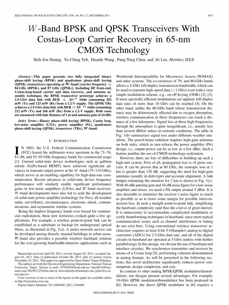
Being the highest frequency bands ever leased for commer-cial exploitation, these new territories evoked quite a few ap-plications. For example, a wireless point-to-point link can beestablished as a substitute or backup for underground opticalfibers, as illustrated in Fig. 1(a). A metro network service canbe developed among densely situated buildings in urban areas.
-band also provides a possible wireless backhaul solutionfor the ever-growing bandwidth-intensive applications such as
Manuscript received April 08, 2011; revised August 02, 2011; accepted Au-gust 02, 2011. Date of publication October 06, 2011; date of current versionNovember 23, 2011. This paper was approved by Guest Editor Yorgos Palaskas.
The authors are with the Electrical Engineering Department, National TaiwanUniversity, Taipei, Taiwan (e-mail: [email protected]; [email protected]; [email protected]; [email protected]; [email protected]).
Color versions of one or more of the figures in this paper are available onlineat http://ieeexplore.ieee.org.
Digital Object Identifier 10.1109/JSSC.2011.2166469
Worldwide Interoperability for Microwave Access (WiMAX)and other systems. The co-existence of 70- and 80-GHz bandsallows a 5-GHz full-duplex transmission bandwidth, which canbe used to transmit high-speed data ( 1 Gb/s) even with a verysimple modulation scheme, e.g., on-off keying (OOK) [2], [3].If more spectrally efficient modulations are applied, full-duplexdata rates of more than 10 Gb/s can be reached [4]. On theother hand, unlike the 60-GHz band whose transmission dis-tance may be deleteriously affected due to oxygen absorption,wireless communication at these frequencies can reach a dis-tance of a few kilometers. Signal loss at these high frequenciesthrough the atmosphere is quite insignificant, i.e., usually lessthan several dB/km unless in extreme conditions. The table inFig. 1(b) summarizes signal loss under different weather situ-ations. The pencil-beam radiation requires high-gain antennason both sides, which in turn relaxes the power amplifier (PA)design, i.e., output power can be as low as a few dBm. Such afeature justifies the use of CMOS technology realization.
However, there are lots of difficulties in building up such ahigh-end system. First of all, propagation loss is of great con-cern. It can be proven that at 80 GHz, the isotropic loss at 1km is greater than 130 dB, suggesting the need for high-gainantennas (usually in dish-type) and accurate alignment. A linkbudget estimating the situation for 2 km is shown in Fig. 1(c).With 40-dBi antenna gain and 10-dB noise figure for a low-noiseamplifier and mixer, we need a PA output around 5 dBm. It isalso desirable to minimize the receiver’s noise figure as muchas possible so as to leave some margin for possible intercon-nection loss. In such a straight point-to-point link, simplifyingthe hardware complexity (and thus the cost) is of great interest.It is unnecessary to accommodate complicated modulation orcostly beamforming techniques in baseband, since more typicalcommunication issues such as channel interference or fadingdo not exist here. Using conventional wireless transceiver ar-chitecture requires at least 6-bit 5-GSample/s analog-to-digitalconverters (ADCs) for 2.5-Gb/s data rate, and all of the digitalcircuits in baseband are operated at 5 Gb/s (unless with furtherparallelizing). In this design, we obviate the use of baseband andinterface circuitry. We synchronize transmitter and receiver bymeans of a Costas loop [5], performing coherent demodulationin analog domain. As will be presented in the following sec-tions, this novel architecture significantly reduces power con-sumption, design complexity, and cost.
In contrast to other analog BPSK/QPSK modulator/demod-ulators, our designs present several advantages. For example,10-Gb/s QPSK modulator/demodulator has been proposed in[6]. However, the direct QPSK modulator in [6] requires a
0018-9200/$26.00 © 2011 IEEE
3034 IEEE JOURNAL OF SOLID-STATE CIRCUITS, VOL. 46, NO. 12, DECEMBER 2011
Fig. 1. (a) Illustration of wireless point-to-point link between high-rise buildings. (b) Mm-wave signal (71–86 GHz) loss for different weather conditions (dB/km).(c) Link budget estimated for 2-km link (40-dBi antenna gain included).
phase shifter to generate I/Q signals. The demodulator alsoneeds delay detection to obviate carrier recovery circuitry,which in turn requires a reference signal to ensure one-symboldelay time. In wireless systems, the finite frequency offset be-tween Tx and Rx makes this approach very difficult to realize.The power consumption (850 mW/650 mW) and chip area
mm in [6] also make it less competitive. Here, we havetwo prototypes, both verified in 65-nm CMOS technology:one implements binary phase-shift keying (BPSK) and theother quadrature phase-shift keying (QPSK). Although not aswidely used in today’s wireless communications, the Costasloop actually provides an efficient solution for frequency offsetissues between transmitter and receiver. Both cases achievelow-error communications (bit error rate (BER) whileconsuming total power (Tx+Rx) of no more than 327 and378 mW, respectively.
This paper is organized as follows. Section II illustrates thecarrier recovery technique and data demodulation for BPSK andQPSK transceivers. Section III presents the transceiver architec-tures, and Section IV describes the building blocks. Section Vanalyzes Costas loop behavior, and Section VI covers the chip-antenna assembly techniques. Complete measurement resultsare illustrated in Section VII, and consideration for future workis discussed in Section VIII. Finally, Section IX concludes thiswork.
II. CARRIER RECOVERY AND DEMODULATION
A. BPSK
In ideal phase-shift keying systems, there is no spectral lineat carrier frequency. However, actual wireless systems alwayscontain mismatches, leading to finite carrier spectral line. The-oretically, it is possible to distill the carrier frequency by placinga high- filter in the Rx front-end. This method is actually notfeasible because (1) the radio frequency (RF) signal capturedfrom the antenna is usually too small to be processed even afterthe amplification of LNA; and (2) it is almost impossible to re-alize a high- ( 50) filter on chip; or (3) even if the carrier
frequency can be obtained, the phase relationship between RFand local-oscillation (LO) signals is still unknown. As a result,we have to look for other nonlinear solutions, and one of thebest candidates is just such a Costas loop.
A Costas loop basically mixes the quadrature LO signals withthe incoming RF, and further blends the two results to obtainthe phase relationship. It provides reasonable performance atlower frequency bands [7]. At millimeter-wave bands, however,the original Costas loop design is quite difficult to apply, be-cause generating very high-speed quadrature signals is not at alltrivial. Meanwhile, clock tuning, loop filter design, and layoutarrangement become challenging as well. The limited capturerange requires a frequency acquisition loop to bring the fre-quency of the voltage-controlled oscillator (VCO) to the desiredvalue before conducting phase locking. To the best of the au-thors’ knowledge, these issues have never been discussed. Wehere propose our novel Costas loop topology in this section.
In order to optimize a coherent demodulation, the LO signalmust be in-phase with the RF signal. Following the idea of amixer-based linear clock and data recovery (CDR) circuit [8],we can obtain the phase relationship by using an additionalmixer. Fig. 2 illustrates this idea. Denoting input data, operationfrequency, phase error, and mixer conversion gain as , ,
, and , respectively, we get two resultsand at the outputs of the two down-conversionmixers, given that the second-order harmonics are fully sup-pressed by the low-pass filters. After further multiplication,we have an output that is proportional to . With enoughgain, if a feedback loop is placed around the VCO (and/or the RFinput), the phase error will be locked at the origin. This leadsto a maximum signal-to-noise ratio (SNR) for the demodulation.Since this approach is purely linear and is operated in near-dcmode, the well-defined linear phase-locked loop (PLL) modelcan be directly applied. As a result, the output data is obtainedat node on phase locking. This phase-locking behavior is verymuch like a linear CDR circuit. Owing to the relatively low in-terference in a pencil-beam radiation system, a stable phase de-tection can be achieved.

HUANG et al.: -BAND BPSK AND QPSK TRANSCEIVERS WITH COSTAS-LOOP CARRIER RECOVERY IN 65-nm CMOS TECHNOLOGY 3035
Fig. 2. Phase detection for BPSK.
Fig. 3. Frequency detection for BPSK (scaling factor not included).
But how to synchronize the frequency in the first place? Here,we resort to auto-correlation to acquire the frequency informa-tion. Suppose the frequency error between RF and LO is definedas . As shown in Fig. 3, we multiply the two temporary out-puts and by themselves, ar-riving at an output proportional to . Here, for sim-plicity we neglect scaling factor such as mixer gain. This result,together with that we just obtained from the phasedetector (PD), reveals frequency information, that is, these twosignals (or equivalently their squared version and ) areseparated by 90 . Whether is leading or lagging dependson the polarity of . In other words, we can detect the sign offrequency error by sampling one signal with the other througha D-flip-flop. The output subsequently drives another -to-converter, which pumps proportional current into the loop filter.Note that we do need limiters here to sharpen the transition of
and , otherwise the D-flip-flop may notfunction properly as the beat frequency approaches zero. Mean-while, as the phase is locked, stays high forever. We thustake to automatically turn off the frequency acquisition loopupon phase lock [9]. This function obviates complex lock de-tection circuitry and saves significant power.
B. QPSK
The carrier recovery approach for BPSK transceivers can bemodified to accommodate QPSK systems. As shown in Fig. 4,
we add limiters and cross correlation to resolve the phase rela-tionship embedded in the quadrature input. Suppose
, where anddenote the input data, and LO signals
and . We therefore have two tentative out-puts and , respectively, after mixing and limiting. Thesetwo signals are further mixed with each other, creating the finaloutput which is proportional to , that is,
(1)
(2)
for . In such a phase region, the limiterswould force to approach unity and to ap-proach zero.1 In other words, , ,and . Note that for simplicity here we omitmixer gain. A -to- converter is placed following the phasedetector to adjust the VCO’s frequency (and its phase) accord-ingly. Once again, we obtain a sinusoidal input-output charac-teristic (Fig. 4), and the approximately linear behavior in thevicinity of origin makes the loop a linear PLL.
The frequency-locking mechanism for QPSK is also shownin Fig. 5. Again, by means of examining the cross and auto-correlation of and twice, we obtain an output containing
1A limiter "digitizes" the input signal. Voltage higher than the middle-linethreshold is considered logic 1 (otherwise logic 0).

3036 IEEE JOURNAL OF SOLID-STATE CIRCUITS, VOL. 46, NO. 12, DECEMBER 2011
Fig. 4. Phase detection for QPSK.
Fig. 5. Frequency detection for QPSK.
the frequency error information. By the same token, if the signalmagnitude is given by , we have
(3)
(4)
It can be easily derived from the self-explanatory illustrationin Fig. 5. The frequency error is obtained by sampling the twoquadrature signals with each other. The final frequency detec-tion result drives another -to- converter to tune the fre-quency. Note that can be used for automatic shut-off func-tion since it stays low when the phase locking is achieved.
III. TRANSCEIVER ARCHITECTURE
Although theoretically attainable, the realization of suchCostas loops involves many physical issues. We implement twotransceivers and present the two cases separately.
A. BPSK
Fig. 6(a) depicts the BPSK transmitter, which includes a full-rate frequency synthesizer providing 84-GHz carrier frequency.A Gilbert-cell-based modulator [10] with rail-to-rail data swingis responsible for 180 phase modulation, and a power am-plifier delivers the RF output to antenna. Such a full-rate di-rect modulation saves significant power and design complexity.The 84-GHz VCO and first divider design will be illustrated inSection IV-C. To further optimize power and performance, thesecond to fourth stages in the divider chain are made of current
Fig. 6. BPSK transceiver architecture. (a) Tx. (b) Rx.
mode logic (CML) static topology [11], whereas the last threestages are realized as true single phase clock (TSPC) structure[12]. A typical type-IV phase and frequency detector (PFD) isadopted in this prototype for simplicity. Second-order loop filteris implemented on chip.
HUANG et al.: -BAND BPSK AND QPSK TRANSCEIVERS WITH COSTAS-LOOP CARRIER RECOVERY IN 65-nm CMOS TECHNOLOGY 3037
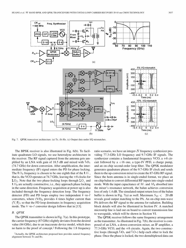
Fig. 7. QPSK transceiver architecture. (a) Tx. (b) Rx. (c) Output data under I/Q mismatches.
The BPSK receiver is also illustrated in Fig. 6(b). To facil-itate quadrature LO signals, we use heterodyne architecture inthe receiver. The RF signal captured from the antenna gets am-plified by an LNA with gain of 18.5 dB and mixed with(74.7 GHz) for down conversion. After amplification, the inter-mediate frequency (IF) signal enters the PD for phase locking.The frequency is chosen to be one eighth that of the ,that is, the VCO operates at 74.7 GHz, leaving the 8 clocks for
. Note that the two phase-locking loops through andare actually constructive, i.e., they approach phase locking
in the same direction. Frequency acquisition at power-up is alsoincluded through the frequency detection loop. The frequencydetector (FD) and PD loops employ two independent -to-converters, where (V/I) provides 4 times higher current than
so that the FD loop dominates in frequency acquisitionmode. The -to- converter design follows that in [13].
B. QPSK
The QPSK transmitter is shown in Fig. 7(a). In this prototype,the carrier frequency (87 GHz) slightly deviates from the desiredvalue (84 GHz), due to an inaccurate device model, which doesno harm to the proof of concept.2 Following the 1:8 frequency
2Actually, the QPSK architecture proposed here provides natural frequencyalignment between Tx and Rx.
ratio scenario, we have an integer- frequency synthesizer pro-viding 77.3-GHz LO frequency and 9.7-GHz IF signals. Thesynthesizer contains a fundamental frequency VCO, a 8 cir-cuit followed by a 16 one, a type-IV PFD, a charge pump,and an on-chip second-order loop filter. The QPSK modulatorgenerates quadrature phases of the 9.7-GHz IF clock and sendsthem to the up-conversion mixer to create the 87-GHz RF signal.Since the horn antenna is in single-ended format, we place anon-chip balun to convert differential RF inputs into single-endedmode. With the input capacitance of and absorbed intothe mixer’s resonance network, the balun achieves conversionloss of only 1.4 dB. The simulated output return loss of the balunbuffer is shown in Fig. 7(a) as well. Maximum 20 dBreveals good output matching to the PA. An on-chip mm-wavePA delivers the RF signal to the antenna for radiation. Buildingblock details will also be illustrated in Section IV. A matchedmicrostrip line is laid out on board to convert transmission lineto waveguide, which will be shown in Section VI.
The QPSK receiver follows the same frequency arrangementas the transmitter. As illustrated in Fig. 7(b), the receiver is com-posed of an LNA, a down-conversion mixer, an IF amplifier, a77.3-GHz VCO, and the 8 circuits. Again, the two construc-tive loops (through and ) help each other to lock thephase. Once the phase is locked, the two demultiplexed data can

3038 IEEE JOURNAL OF SOLID-STATE CIRCUITS, VOL. 46, NO. 12, DECEMBER 2011
Fig. 8. Simulation of locking behavior for (a) BPSK and (b) QPSK TRxs.
Fig. 9. (a) LNA. (b) IF amplifier. (c) Down-conversion mixer. (d) BPSK modulator.
be obtained at nodes and . The PD and FD are responsiblefor phase and frequency detection as described in the previoussection. In circuit realization, the finite I/Q mismatch wouldcause jitter in the output data. As shown in Fig. 7(c), output datajitter increases from 55 ps (perfectly balance I/Q) to 60 ps (5%mismatch) and 70 ps (10% mismatch).
In addition to higher data rate, another important advantageof QPSK structure is that the transmitter’s VCO design can bereused in the receiver, eliminating possible frequency offset be-tween Tx and Rx.3 Again, the automatic FD shut-down functionis preserved, and carries 4 times larger current than the
does to ensure a good frequency acquisition procedure.All blocks are implemented on chip including the loop filter.To verify the locking behavior, we plot the simulated controlvoltage around start-up points for both BPSK and QPSK trans-
3Of course, external issues such as temperature difference between Tx andRx are not considered here.
ceivers in Fig. 8. Phase locking can be achieved within approx-imately 3.2 s and 150 ns, respectively, if the loop filters haveno charge initially (i.e., at ).
IV. BUILDING BLOCKS
Here, we introduce circuit details of building blocks and theirdesign considerations.
A. LNA
Fig. 9(a) shows the LNA design. Modified from [14], threegain stages are cascaded with conjugate matching in between toachieve power gain of 18.5 dB. Since the skin depth at 87 GHz(0.22 m) is larger than the thickness of metal 1 (0.18 m),we shunt two bottom layers (M1 and M2) as a ground planeto reduce leakage. and are laid out with shared junctionto minimize the parasitic capacitance [15].

HUANG et al.: -BAND BPSK AND QPSK TRANSCEIVERS WITH COSTAS-LOOP CARRIER RECOVERY IN 65-nm CMOS TECHNOLOGY 3039
Fig. 10. (a) VCO and first frequency divider. (b) Power amplifier. (c) QPSK modulator.
B. IF Amplifier, Mixer, and BPSK Modulator
The IF amplifier utilizes five stages with ac-coupling andself-biasing to suppress offset, and under-damped loading isused to increase the gain while saving power [Fig. 9(b)] [16].The first and fourthe stages incorporate local feedback resistor
to fulfill self-biasing input, whereas the second, third, andfifth stages employ regular differential pair structure with in-ductive peaking. Overall power consumption for the five stagesis equal to 25 mW. The down-conversion mixer is realized asshown in Fig. 9(c) [17], where the gain stage andswitching stages are separated with ac-coupling inbetween. The single-ended RF signal is sent to one common-source node , whose parasitic capacitance is absorbed into thematching network. This topology manifests itself in advancedCMOS technology, where the supply voltage is as low as 1.01.2 V. The mixer gain is given by 4.5 dB. The BPSK modulatoris illustrated in Fig. 9(d), where a Gilbert-cell-based structure[10] is used but with rail-to-rail data switching and no tail cur-rent. Only a single end is taken out as RF output since the PAis single-ended as well. Consuming 16 mW of power, this mod-ulator presents saturated power of 4 dBm. Other possible real-ization can be found in [18]. Simulated output waveform underdata transition is also shown in Fig. 9(d).
C. VCO and First Divider
The VCO and the first frequency divider are shown inFig. 10(a). The VCO incorporates a cross-coupled oscil-lator with thick-oxide (5.6 nm) varactors, which is followed bytwo tuned amplifiers as buffers. The 84- [BPSK Tx, Fig. 6(a)],74.7- [BPSK Rx, Fig. 6(b)], and 77.3-GHz (QPSK TRx,Fig. 7) VCOs achieve tuning range of 0.9, 1.0, and 1.0 GHz,respectively. Note that the Tx and the Rx VCOs in the QPSKsystem are made in identical sizes due to our frequency ar-rangement. The first frequency divider is realized as a directinjection-locked topology, where the injection signal is ac-cou-pled to the gate of the switch . Dummy loadings arecarefully added to balance the parasitics. The minimum dividerlock range in the two TRx prototypes here is approximatelyequal to 3.8 GHz with 0.8 V. The lock range and self-os-cillation frequency of the divider with respect to are alsoplotted in Fig. 10(a). Simulation shows that locking can beensured over PVT variation by setting 0.8 V.
D. Power Amplifier and QPSK Modulator
The power amplifier design [Fig. 10(b)] is also modified fromthat in [14]. To ensure stability, a local bypass network is placedat each of the five gain stages, where , are used to lower

3040 IEEE JOURNAL OF SOLID-STATE CIRCUITS, VOL. 46, NO. 12, DECEMBER 2011
Fig. 11. (a) 2:1 selector for QPSK. (b) Up-conversion mixer.
Fig. 12. (a) Costas loop behavior model. (b) Input–output characteristic for both cases.
both the impedance and quality factor of the network. ThePA is designed to have power gain of 14.8 dB while consuming129 mW from a 1.2-V supply.
The QPSK modulator is shown in Fig. 10(c). A demultiplexerparallelizes the input data into two half-rate data streams and amapping logic rearranges the data sequences. After retiming,two outputs are created, controlling the IF 2:1 selector and themultiplier. As a result, 9.7-GHz clocks with four possible phasesare produced. Note that the multiplier is placed after the selectorto suppress the I/Q mismatch, because the distance of separateI/Q paths can be minimized by doing so.
E. 2:1 Selector, Multiplier, and Up-Conversion Mixer
The 2:1 selector and multiplier are shown in Fig. 11(a). Theyare modified from standard Gilbert cells with tail currents takenoff, i.e., making data swing rail-to-rail to speed up the opera-tion. Again, to accommodate low supply voltage, the selectionthrough and are separated in two stages. Switches
are added to block the clock feedthrough, other-wise the unwanted signal would penetrate into the output port.
Fig. 11(b) illustrates the up-conversion mixer. It has a similarstructure but with inductive loading, which resonates at 87 GHz.With class-AB biasing [19] in the lower stage and ac-coupledinputs, the mixer achieves a gain of 0.4 dB, and a 3-dB band-width of 10 GHz while consuming 9 mW of power. The fol-lowing balun buffer reveals 5-dB gain, and its 3-dB bandwidthis simulated to be 17 GHz.
V. COSTAS LOOP MODELING
The Costas loop behavior needs further study in our particularsystem to ensure stability. As depicted in Fig. 12(a), with onefeedback going to RF mixer and the other to PD, we derive phaserelationship as
(5)
(6)
where , , and denote the gain of PD, -to- con-verter, and VCO, respectively. It follows that
(7)
in which
(8)
As expected, the dual PLL is equivalent to a single PLL witha divide ratio of 9/8. In our designs, we have190 A/rad, for QPSK and BPSK trans-ceivers. The simulated magnitude as a function of phase changerate is shown in Fig. 12(b), suggesting a bandwidth of 3 MHz forBPSK TRx and 80 MHz for QPSK TRx. With the coefficientsused in this design, all of the poles are located in the left-handside of the -plane, implying system stability. The phase margin

HUANG et al.: -BAND BPSK AND QPSK TRANSCEIVERS WITH COSTAS-LOOP CARRIER RECOVERY IN 65-nm CMOS TECHNOLOGY 3041
Fig. 13. (a) Waveguide adapter and (b) its insertion loss, (c) assembly photograph, and (d) layout and EM simulation.
Fig. 14. (a) Die photographs and power consumption. (b) Testing setup.
for BPSK and QPSK are both 75 . Transistor-level simulationensures sufficient phase margin over PVT variations.
VI. CHIP-ANTENNA ASSEMBLY
The interconnection between chip and antenna is of great im-portance as well. Conventional structures such as probe-fed type[20], slot-coupled type [21], and quasi-Yagi antenna type [22]are usually too costly and too complex for system integration.As shown in Fig. 13(a), we realize the coplanar strip to wave-guide by a transition fabricated on a single-layer dielectric sub-strate [23]. With the chip flipped onto the microstrip line, theRF signal is coupled to the matching element through the sub-strate, which is connected to the waveguide (i.e., entrance ofhorn) tightly. In other words, the signal power is transferred by
Fig. 15. (a) LNA and (b) PA measurement.
matched coupling. Note that no expensive or bulky matchingnetwork is required here since resonance of matching el-ement can efficiently convert quasi-TEM mode (in microstripline) to mode (in waveguide). The measured insertion lossof the transition is depicted in Fig. 13(b), where the maximumloss from 81–86 GHz is less than 5.3 dB. Fig. 13(c) illustratesa photograph of the assembly. The layout of waveguide transi-tion and its EM simulation result is also illustrated in Fig. 13(d).Since the minimum allowable distance between vias on boardis 150 m, we can hardly create a very nice resonance cavityat 84 GHz. As a result, a low-cost transition with moderate per-formance has been created. Actually, a total loss of 4 5 dB isintroduced here. The horn antennas we used here have 24-dBigain for each.
VII. EXPERIMENTAL RESULTS
The BPSK and QPSK transceivers are both fabricated in65-nm CMOS technology. The photographs of the dies areshown in Fig. 14(a) with the chip sizes listed below. Individualblocks such as LNA and PA are measured independently. Forthe BPSK TRx, the transmitter consumes 202 mW and the

3042 IEEE JOURNAL OF SOLID-STATE CIRCUITS, VOL. 46, NO. 12, DECEMBER 2011
Fig. 16. (a) Spectrum of 84-GHz carrier in BPSK Tx. (b) Detailed phase noise plot of (a). (c) Spectrum of BPSK Tx output under data transmission (data rate �650 Mb/s, � � � PRBS). (d) Tx output spectrum for data rate � 2.5 Gb/s (� � � PRBS).
receiver 125 mW. The QPSK transmitter dissipates 212 mWand the receiver 166 mW. All circuits are operated with a1.2-V supply. Note that measurements such as recovered dataeye diagrams are conducted by a link through the air, wherethe Tx and Rx are separated by 1 m. The testing setup is alsoshown in Fig. 14(b). Different data rate, and data patterns havebeen tested through a coaxial cable. Individual blocks are fullyverified as well. We summarize the results in this section.
A. Millimeter-Wave Components
The LNA performance has been presented in Fig. 15(a). Thesmall-signal measurement shows maximum gain of 18.5 dB anda minimum input return loss of 27 dB. The 10-dB bandwidthfor and are 10 and 11 GHz, respectively. The noisefigure in the band of interest is less than 6.9 dB. The input 1-dBcompression point is given by 22 dBm, and inputthird-order intercept point is equal to 12.5 dBm.
The PA’s measurement result is also demonstrated inFig. 15(b). It shows 14.8-dB gain and 10-dB output return lossat 87 GHz. Large-signal results reveal output 6.5 dBm,saturatio2n power 10.2 dBm, and maximum poweradded efficiency .
B. BPSK TRx
For BPSK chips, the 84-GHz carrier spectrum in contin-uous mode is plotted in Fig. 16(a), implying phase noise of
89.1 dBc/Hz at 1-MHz and 103 dBc/Hz at 10-MHz offset.
The phase noise plot of the 662-MHz reference is also demon-strated, revealing 43-dB difference between the two (due tofrequency ratio). A precise phase noise plot [Fig. 16(b)] revealsan integrated rms jitter of 248 fs (integrated from 100 Hz to1 GHz). Under BPSK modulation, the spectrum becomes asinc function around the carrier frequency. Fig. 16(c) illustratesthe spectrum with 650-Mb/s, pseudo random binarysequence (PRBS) data input. The case for higher data rate(2.5 Gb/s) is also shown in Fig. 16(d). In the receive side,the recovered clock spectrum is demonstrated in Fig. 17(a),revealing phase noise of 91.0 dBc/Hz at 10-MHz offset.Here, through the 1-m air link, the transmitted data is a PRBSof length at 2.5 Gb/s. The recovered data waveformis shown in Fig. 17(b). The data jitter measures 13.74 ps,rmsand 100 ps,pp, respectively. Due to the lack of a high-speedreal-time oscilloscope and wideband down-convert mixer, wewere unable to measure the constellation diagram. Note that aCDR can be placed behind the receiver to further clean up thejitter.
C. QPSK TRx
In the 87-GHz QPSK TRx, the carrier (at a fixed frequency)shows a spectrum with phase noise of 85.8 and 106 dBc/Hzat 1-MHz and 10-MHz offsets, respectively [Fig. 18(a)]. Themodulated spectrum (with 650-Mb/s, PRBS data input)is also demonstrated in Fig. 18(b). Note that the bandwidthof the main lobe in QPSK is only half of that in BPSK with

HUANG et al.: -BAND BPSK AND QPSK TRANSCEIVERS WITH COSTAS-LOOP CARRIER RECOVERY IN 65-nm CMOS TECHNOLOGY 3043
Fig. 17. (a) Spectrum of recovered clock in BPSK Rx. (b) Waveform of recovered data (data rate � 2.5 Gb/s, � �� PRBS, vertical scale: 100 mV/div, horizontalscale: 100 ps/div).
Fig. 18. (a) Spectrum of 87-GHz carrier in QPSK Tx. (b) Spectrum of QPSK Tx output under data transmission (data rate � 650 Mb/s, � � � PRBS). (c) Txoutput spectrum for data rate � 2.5 Gb/s (� � � PRBS).
the same data rate, as expected. The case for higher data rate(2.5 Gb/s) is also shown in Fig. 18(c). Due to the high loss( 40 dB) of the external harmonic mixer (Agilent 11970W),side lobes are somewhat buried in the noise floor. The recoveredclock spectrum is shown in Fig. 19(a), suggesting a phase noiseof 93.8 dBc/Hz at 5-MHz offset. The two recovered data
streams are depicted in Fig. 19(b). At data rate of 2.5 Gb/s,the data jitter measures 37 ps,rms and 182 ps,pp, respectively.Here, the air link distance 1 m and antenna gain 24 dBi.We have also conducted a BER test (through a coaxial cablelink between Tx and Rx) as shown in Fig. 20. For BPSK,this stays less than until 2.5 Gb/s for a PRBS of length

3044 IEEE JOURNAL OF SOLID-STATE CIRCUITS, VOL. 46, NO. 12, DECEMBER 2011
Fig. 19. (a) Spectrum of recovered clock in QPSK Rx. (b) Waveform of recovered data (data rate � 2.5 Gb/s, � �� PRBS, vertical scale: 100 mV/div, horizontalscale: 200 ps/div).
. For QPSK, on the other hand, BER can be less thanuntil 3.5 Gb/s for a PRBS of length .4 Note that
a Costas loop actually behaves as a clock and data recoverycircuit. Sequences with longer consecutive bits leads to carrierphase wander and therefore higher BER. Table I summarizesthe overall performance, and compares this work with someother mm-wave transceivers recently published [18], [24], [25].A better Tx output power can be expected in future design ifwe can shift the peaking frequencies of all resonance networksto exactly 84 GHz. Our circuits require no baseband circuitry,achieving data rate of at least 2.5 Gb/s while consuming only327 and 378 mW of power for BPSK TRx and QPSK TRx,respectively. The carrier frequency offset (from desired 84 GHzto 87 GHz) degrades the PA gain and thus output power slightly.
VIII. FUTURE WORK
These prototypes demonstrate fundamental -band opera-tion and baseband-less carrier recovery. However, some fea-tures of these works can be further improved. For example, thebasic BPSK/QPSK modulations are vulnerable to noise or inter-ference that may possibly cause “false” phase locking, that is,there are two and four possible phase locking points (0 /180 ,0 /90 /180 /270 ) for BPSK and QPSK receiver respectively.
4The loop capacitor of the QPSK TRx is realized on chip, minimizing un-wanted noise coupling. Perhaps it explains why the QPSK TRx achieves betterBER.
Fig. 20. BER for (a) BPSK and (b) QPSK TRx (through a coaxial cable linkbetween Tx and Rx).
As SNR decreases, the outputs of I and Q channels may be al-tered during demodulation. This phase ambiguity issue can beresolved by placing differential coding mechanism into the TRx.Instead of using the bit patterns to set up the carrier phase, differ-ential PSKs (e.g., DBPSK or DQPSK) use phase change (ratherthan the phase itself) to distinguish the Ones from the Zeros.Since this scheme depends on the difference between successivephases, the data patterns can be recovered in the receiver sidecorrectly. An additional wideband CDR at the Rx’s output maybe necessary for decoding and further data jitter clean-up. Note

HUANG et al.: -BAND BPSK AND QPSK TRANSCEIVERS WITH COSTAS-LOOP CARRIER RECOVERY IN 65-nm CMOS TECHNOLOGY 3045
TABLE IPERFORMANCE SUMMARY
that, in our testing, false locking does not occur because the SNRis quite high , but future redesign for long-dis-tance application must take this issue into consideration.
IX. CONCLUSION
This work presents an analog carrier recovery technique ap-plied to BPSK and QPSK transceivers operating at 80–90 GHz.Achieving very simple structures and very low power consump-tion, these chips provide promising potential for next generationwireless point-to-point data links.
ACKNOWLEDGMENT
The authors thank the TSMC University Shuttle Program forchip fabrication.
REFERENCES
[1] “Allocations and service rules for the 71–76 GHz, 81–86 GHz, and92–95 GHz bands,” FCC Notice of Proposed Rule Making 02-180, Jun.2002.
[2] J. Lee et al., “A low-power low-cost fully-integrated 60-GHz trans-ceiver system with OOK modulation and on-board antenna assembly,”IEEE J. Solid-State Circuits, vol. 45, no. 2, pp. 264–275, Feb. 2010.
[3] F. Lin et al., “A low power 60 GHz OOK transceiver system in 90 nmCMOS with innovative on-chip AMC antenna,” in Proc. IEEE AsianSolid-State Circuits Conf., 2009, pp. 349–354.
[4] J. Wells, “Multigigabit wireless connectivity at 70, 80 and 90 GHz,”RF Design Mag., vol. 29, pp. 50–59, May 2006.
[5] J. P. Costas et al., “Synchronous communications,” Proc. IRE, vol. 44,pp. 1713–1718, Dec. 1956.
[6] H. Takahashi et al., “10-Gbit/s QPSK modulator and demodulator fora 120-GHz-band wireless link,” in IEEE IMS Dig., May 2010, pp.632–635.
[7] C. Chien et al., “A single-chip 12.7 Mchips/s digital IF BPSK direct se-quence spread-spectrum transceiver in 1.2 �m CMOS,” IEEE J. Solid-State Circuits, vol. 29, no. 12, pp. 1614–1623, Dec. 1994.
[8] J. Lee et al., “A 20-Gb/s full-rate linear clock and data recovery circuitwith automatic frequency acquisition,” IEEE J. Solid-State Circuits,vol. 44, no. 2, pp. 264–275, Dec. 2009.
[9] J. Lee et al., “A 75-GHz phase-locked loop in 90-nm CMOS tech-nique,” IEEE J. Solid-State Circuits, vol. 43, no. 6, pp. 1414–1426,Jun. 2008.
[10] B. Gilbert, “A precise four-quadrant multiplier with subnanosecondresponse,” IEEE J. Solid-State Circuits, vol. SC-3, no. 4, pp. 365–373,Dec. 1968.
[11] B. Razavi et al., “A 13.4-GHz CMOS frquency divider,” in IEEE Int.Solid-State Circuits Conf. (ISSCC) Dig. Tech. Papers, Feb. 1994, pp.224–225.
[12] J. Yuan et al., “High-speed CMOS circuit technique,” IEEE J. Solid-State Circuits, vol. 24, no. , pp. 62–70, Feb. 1989.
[13] J. Lee, “A 20-Gb/s adaptive equalizer in 0.13- �m CMOS technology,”IEEE J. Solid-State Circuits, vol. 41, no. 9, pp. 2058–2066, Sep. 2006.
[14] J. Lee et al., “A fully-integrated 77-GHz FMCW radar transceiver in65-nm CMOS technology,” IEEE J. Solid-State Circuits, vol. 45, no.12, pp. 2746–2756, Dec. 2010.
[15] B. Heydari et al., “A 60-GHz 90-nm CMOS cascode amplifier withinterstage matching,” in Proc. Eur. Microw. Integr. Circuit Conf., Oct.2007, pp. 88–91.
[16] H. Wang et al., “A 60-GHz FSK transceiver with automatically-cal-ibrated demodulator in 90-nm CMOS,” in Symp. VLSI Circuits Dig.Tech. Papers, Jun. 2010, pp. 95–96.
[17] B. Razavi, “A millimeter-wave CMOS heterodyne receiver withon-chip LO and divider,” IEEE J. Solid-State Circuits, vol. 43, no. 2,pp. 477–485, Feb. 2008.
[18] A. Tomkins et al., “A zero-IF 60 GHz 65 nm CMOS transceiver withdirect BPSK modulation demonstrating up to 6 Gb/s data rates overa 2 m wireless link,” IEEE J. Solid-State Circuits, vol. 44, no. 8, pp.2085–2099, Aug. 2009.
[19] J. Lee et al., “A 40-Gb/s clock and data recovery circuit in 0.18-gmCMOS technology,” IEEE J. Solid-State Circuits, vol. 38, no. 12, pp.2181–2190, Dec. 2003.
[20] Y. Shih et al., “A waveguide-to-microstrip transitions for mil-limeter-wave applications,” in IEEE MTT-S Int. Microw. Symp. Dig.,May 1988, vol. 1, pp. 473–475.
[21] Y. Shih et al., “Microstrip to waveguide transition compatible withMM-wave integrated circuits,” IEEE Trans. Microw. Theory Tech., vol.42, no. 9, pp. 1842–1843, Sep. 1994.

3046 IEEE JOURNAL OF SOLID-STATE CIRCUITS, VOL. 46, NO. 12, DECEMBER 2011
[22] N. Kaneda et al., “A broadband microstrip-to-waveguide transitionusing quasi-yagi antenna,” IEEE Trans. Microw. Theory Tech., vol. 47,no. 12, pp. 2562–2567, Dec. 1999.
[23] H. Iizuka et al., “Millimeter-wave microstrip line to waveguide tran-sition fabricated on a single layer dielectric substrate,” IEICE Trans.Commun., pp. 1169–1177, Jun. 2002.
[24] C. Marcu et al., “A 90 nm CMOS low-power 60 GHz transceiver withintegrated baseband circuitry,” IEEE J. Solid-State Circuits, vol. 44, no.12, pp. 3434–3447, Dec. 2009.
[25] I. Sarkas et al., “An 18-Gb/s, direct QPSK modulation, SiGe BiCMOStransceiver for last mile links in the 70–80 GHz band,” IEEE J. Solid-State Circuits, vol. 45, no. 10, pp. 1968–1980, Oct. 2010.
Shih-Jou Huang was born in Tainan, Taiwan, in1986. He received the B.S. degree in electricalengineering from National Tsing-Hua University,Hsinchu, Taiwan, in 2008. He is currently workingtoward the Ph.D. degree at the Graduate Institute ofElectrical Engineering, National Taiwan University,Taipei, Taiwan.
His research interests focus on millimeter-wavewireless transceivers.
Yu-Ching Yeh was born in Nantou, Taiwan, in 1987.She received the B.S. and M.S. degrees in electricalengineering from National Taiwan University, Taipei,Taiwan, in 2009 and 2011, respectively. She is cur-rently working toward the Ph.D. degree at the Uni-versity of California, Berkeley.
Her research interests focus on millimeter-wavewireless transceivers.
Huaide Wang received the B.Sc., M.S., and Ph.D.degrees from National Taiwan University (NTU),Taipei, Taiwan, in 2006 and 2010, respectively, allin electrical engineering.
He joined MediaTek Inc., Hsinchu, Taiwan, in2010, where he is currently a Senior Engineer.His research interests include phase-locked loops,high-speed SerDes, and backplane transceivers.
Pang-Ning Chen was born in Taipei, Taiwan, in1986. He received the B.S. degree in electricalengineering from National Chiao Tung University,Hsinchu, Taiwan, in 2008. He is currently workingtoward the Ph.D. degree at the Graduate Institute ofElectrical Engineering, National Taiwan University,Taipei, Taiwan.
His research interests focus on millimeter-wavewireless transceivers.
Jri Lee (S’03–M’04) received the B.Sc. degree fromNational Taiwan University (NTU), Taipei, Taiwan,in 1995, and the M.S. and Ph.D. degrees from theUniversity of California, Los Angeles (UCLA), bothin 2003, all in electrical engineering.
After two years of military service (1995–1997),he was with Academia Sinica, Taipei, Taiwan from1997 to 1998, and subsequently Intel Corporationfrom 2000 to 2002. He joined National TaiwanUniversity (NTU) in 2004, where he is currentlya Professor of electrical engineering. His current
research interests include high-speed wireless and wireline transceivers,phase-locked loops, and applications, and mm-wave circuits.
Prof. Lee received the Beatrice Winner Award for Editorial Excellence at the2007 ISSCC, the Takuo Sugano Award for Outstanding Far-East Paper at the2008 ISSCC, the Best Technical Paper Award from Y. Z. Hsu Memorial Foun-dation in 2008, the T. Y. Wu Memorial Award from National Science Council(NSC), Taiwan in 2008, the Young Scientist Research Award from AcademiaSinica in 2009, and the Outstanding Young Electrical Engineer Award in 2009.He has also received NTU outstanding teaching award in 2007, 2008, and 2009.He has worked as a guest editor of the IEEE JOURNAL OF SOLID-STATE CIRCUITS
in 2008. He is currently a Distinguished Lecturer of the IEEE Solid-State Cir-cuits Society (SSCS). He has been serving in the Technical Program Commit-tees of the International Solid-State Circuits Conference (ISSCC, 2007–2010),Symposium on VLSI Circuits (2008–present), and Asian Solid-State CircuitsConference (A-SSCC, 2005–present).


![IEEE JOURNAL OF SOLID-STATE CIRCUITS, VOL. 46, NO. 1, JANUARY 2011 …ssl.kaist.ac.kr/2007/data/journal/[2011_JSSC]LongYan.pdf · 2019. 3. 5. · IEEE JOURNAL OF SOLID-STATE CIRCUITS,](https://static.fdocuments.us/doc/165x107/6115b590491e02457105dd76/ieee-journal-of-solid-state-circuits-vol-46-no-1-january-2011-sslkaistackr2007datajournal2011jssc.jpg)


