IEEE JOURNAL OF SOLID-STATE CIRCUITS, VOL. 41, …theo.scu.ac.ir/_Engineering/Documents/Analog AGC...
10
IEEE JOURNAL OF SOLID-STATE CIRCUITS, VOL. 41, NO. 10, OCTOBER 2006 2291 Analog AGC Circuitry for a CMOS WLAN Receiver Okjune Jeon, Member, IEEE, Robert M. Fox, Senior Member, IEEE, and Brent A. Myers, Member, IEEE Abstract—The IEEE 802.11a standard uses orthogonal fre- quency division multiplexing (OFDM) to allow high data rates in multipath WLAN environments. The high peak-to-average power ratio (PAPR) of OFDM signals, along with stringent settling-time constraints, make conventional closed-loop automatic gain control (AGC) schemes impractical for WLAN receivers. In a direct con- version receiver, AGC and channel-select filtering are performed by analog baseband circuitry. A baseband signal processor using a new open-loop analog gain-control algorithm for OFDM is de- scribed. The new AGC algorithm uses switched coarse gain-setting steps followed by an analog open-loop fine gain-setting step to set the final gain of variable gain amplifiers (VGAs). The AGC was implemented in a 0.18- m CMOS process using newly designed circuits including linear VGAs, RMS detectors, and current-mode computation circuitry. Simulation and measurement results verify that the new AGC circuit converges with gain error less than 1 dB to the desired level within 5.6 s. Index Terms—Automatic gain control (AGC), CMOS integrated circuits, IEEE 802.11a, OFDM, translinear circuits, variable gain amplifier (VGA), wireless LAN. I. INTRODUCTION A UTOMATIC gain control (AGC) is an essential func- tion in wireless local-area network (WLAN) receivers because the power received through the wireless channel is unpredictable. The AGC circuitry maintains a desired output signal amplitude with input signals of variable strength. In the IEEE 802.11a WLAN system, data pass through the channel in packets consisting of preamble, header and data segments. The receiver estimates the channel’s characteristics during reception of the preamble. These characteristics are assumed to stay constant throughout the transmission of the whole packet, typically up to 1 ms. The preamble consists of 10 repetitions of a predefined data stream called a short training symbol (10 0.8 s) and two repetitions of a long training symbol (2 4 s). While multipath effects can significantly alter the waveform, the channel characteristics change slowly enough to be considered constant throughout the entire packet. Thus, the received signal is essentially repeated during each short training symbol time, and its characteristics are used to establish the amplitude and phase references for the whole packet. In the proposed receiver system, seven of the repeated short training symbols (5.6 s) are used for AGC convergence [1]. Once the gain has been optimized, the rest of the preamble time is available to the digital signal processor (DSP). Manuscript received December 22, 2005; revised April 24, 2006. O. Jeon and R. M. Fox are with the Department of Electrical and Computer Engineering, University of Florida, Gainesville, FL 32611-6130 USA (e-mail: [email protected]fl.edu). B. A. Myers is with Conexant Systems, Melbourne, FL 32901 USA (e-mail: [email protected]). Digital Object Identifier 10.1109/JSSC.2006.881548 Fig. 1. Conventional AGC loop composed of VGA, peak detector, and loop filter. Conventional closed-loop analog AGCs use feedback loops to adjust the gain of the variable-gain amplifiers (VGA) to get the desired output signal strength. In such AGC loops, as shown in Fig. 1, signal amplitude is typically estimated using a peak de- tector. This adequately represents the amplitude of signals with fixed peak-to-average power ratio (PAPR) such as sinusoids, but is unreliable for high-PAPR signals. The problem is worsened by the short time (0.8 s) available for estimating amplitude in 802.11a applications. For proper operation of closed-loop AGCs, the time to determine amplitude must be much less than the time constant of the loop filter [2]. As the input amplitude changes, the detected output amplitude is compared to the de- sired DC amplitude and the difference error is fed back to adjust the gain of the VGA to provide constant output amplitude. The negative feedback loop continuously responds to input ampli- tude variation, but for stability the loop response must be slow. These issues precluded the use of a conventional AGC loop in this application. The baseband processor presented here uses a new open-loop AGC algorithm. The AGC uses pseudo-RMS detection, which has been found to be adequate for estimating OFDM amplitude using received 0.8 s short training symbols [3]. The AGC sets gain to within 1 dB of its optimal value within the time for seven short training symbols. Many WLAN receivers use digital signal processing to im- plement much of the AGC function. Implementing the AGC in analog circuitry offers lower system power, allowing the DSP to sleep most of the time, using the analog chain to monitor activity. The analog approach presented here can also reduce circuit complexity by eliminating digital-to-analog conversion for the gain control, and avoiding the need for calibrated gain stages. Section II of this paper describes the receiver architecture and the gain and filtering requirements for the analog baseband signal chain. Section III describes the new open-loop AGC 0018-9200/$20.00 © 2006 IEEE
-
Upload
trinhthuan -
Category
Documents
-
view
216 -
download
0
Transcript of IEEE JOURNAL OF SOLID-STATE CIRCUITS, VOL. 41, …theo.scu.ac.ir/_Engineering/Documents/Analog AGC...

IEEE JOURNAL OF SOLID-STATE CIRCUITS, VOL. 41, NO. 10, OCTOBER 2006 2291
Analog AGC Circuitry for a CMOS WLAN ReceiverOkjune Jeon, Member, IEEE, Robert M. Fox, Senior Member, IEEE, and Brent A. Myers, Member, IEEE
Abstract—The IEEE 802.11a standard uses orthogonal fre-quency division multiplexing (OFDM) to allow high data rates inmultipath WLAN environments. The high peak-to-average powerratio (PAPR) of OFDM signals, along with stringent settling-timeconstraints, make conventional closed-loop automatic gain control(AGC) schemes impractical for WLAN receivers. In a direct con-version receiver, AGC and channel-select filtering are performedby analog baseband circuitry. A baseband signal processor usinga new open-loop analog gain-control algorithm for OFDM is de-scribed. The new AGC algorithm uses switched coarse gain-settingsteps followed by an analog open-loop fine gain-setting step to setthe final gain of variable gain amplifiers (VGAs). The AGC wasimplemented in a 0.18- m CMOS process using newly designedcircuits including linear VGAs, RMS detectors, and current-modecomputation circuitry. Simulation and measurement results verifythat the new AGC circuit converges with gain error less than 1 dBto the desired level within 5.6 s.
Index Terms—Automatic gain control (AGC), CMOS integratedcircuits, IEEE 802.11a, OFDM, translinear circuits, variable gainamplifier (VGA), wireless LAN.
I. INTRODUCTION
AUTOMATIC gain control (AGC) is an essential func-tion in wireless local-area network (WLAN) receivers
because the power received through the wireless channel isunpredictable. The AGC circuitry maintains a desired outputsignal amplitude with input signals of variable strength. In theIEEE 802.11a WLAN system, data pass through the channelin packets consisting of preamble, header and data segments.The receiver estimates the channel’s characteristics duringreception of the preamble. These characteristics are assumed tostay constant throughout the transmission of the whole packet,typically up to 1 ms. The preamble consists of 10 repetitionsof a predefined data stream called a short training symbol(10 0.8 s) and two repetitions of a long training symbol(2 4 s). While multipath effects can significantly alter thewaveform, the channel characteristics change slowly enough tobe considered constant throughout the entire packet. Thus, thereceived signal is essentially repeated during each short trainingsymbol time, and its characteristics are used to establish theamplitude and phase references for the whole packet. In theproposed receiver system, seven of the repeated short trainingsymbols (5.6 s) are used for AGC convergence [1]. Oncethe gain has been optimized, the rest of the preamble time isavailable to the digital signal processor (DSP).
Manuscript received December 22, 2005; revised April 24, 2006.O. Jeon and R. M. Fox are with the Department of Electrical and Computer
Engineering, University of Florida, Gainesville, FL 32611-6130 USA (e-mail:[email protected]).
B. A. Myers is with Conexant Systems, Melbourne, FL 32901 USA (e-mail:[email protected]).
Digital Object Identifier 10.1109/JSSC.2006.881548
Fig. 1. Conventional AGC loop composed of VGA, peak detector, and loopfilter.
Conventional closed-loop analog AGCs use feedback loopsto adjust the gain of the variable-gain amplifiers (VGA) to getthe desired output signal strength. In such AGC loops, as shownin Fig. 1, signal amplitude is typically estimated using a peak de-tector. This adequately represents the amplitude of signals withfixed peak-to-average power ratio (PAPR) such as sinusoids, butis unreliable for high-PAPR signals. The problem is worsenedby the short time (0.8 s) available for estimating amplitudein 802.11a applications. For proper operation of closed-loopAGCs, the time to determine amplitude must be much less thanthe time constant of the loop filter [2]. As the input amplitudechanges, the detected output amplitude is compared to the de-sired DC amplitude and the difference error is fed back to adjustthe gain of the VGA to provide constant output amplitude. Thenegative feedback loop continuously responds to input ampli-tude variation, but for stability the loop response must be slow.
These issues precluded the use of a conventional AGC loopin this application. The baseband processor presented here usesa new open-loop AGC algorithm. The AGC uses pseudo-RMSdetection, which has been found to be adequate for estimatingOFDM amplitude using received 0.8 s short training symbols[3]. The AGC sets gain to within 1 dB of its optimal value withinthe time for seven short training symbols.
Many WLAN receivers use digital signal processing to im-plement much of the AGC function. Implementing the AGC inanalog circuitry offers lower system power, allowing the DSPto sleep most of the time, using the analog chain to monitoractivity. The analog approach presented here can also reducecircuit complexity by eliminating digital-to-analog conversionfor the gain control, and avoiding the need for calibrated gainstages.
Section II of this paper describes the receiver architectureand the gain and filtering requirements for the analog basebandsignal chain. Section III describes the new open-loop AGC
0018-9200/$20.00 © 2006 IEEE

2292 IEEE JOURNAL OF SOLID-STATE CIRCUITS, VOL. 41, NO. 10, OCTOBER 2006
Fig. 2. Architecture for the 5-GHz WLAN receiver.
Fig. 3. Receiver gain distribution plots for 6 and 54 Mb/s data rates.
algorithm. Implementation of the AGC circuit and verifica-tion through simulations and measurements are described inSections IV and V.
II. ANALOG BASEBAND SIGNAL CHAIN
Direct conversion is usually preferred over superheterodynearchitectures for fully integrated WLAN receivers because itssimplicity outweighs drawbacks such as 1/f noise and DC-offset
sensitivity [4]. The baseband processor described here is partof a direct-conversion receiver. As depicted in Fig. 2, the re-ceiver consists of a bandpass filter, low-noise amplifier (LNA),plus mixers, low-pass filters, AGC amplifiers, and analog-to-digital (A/D) converters for the I and Q channels. The RF por-tions of the receiver have the following gains: 3 dB for the(off-chip) bandpass filter, 0 or 20 dB (selectable) for the LNAand 10 dB for the mixers. The AGC amplifiers supply the rest

JEON et al.: ANALOG AGC CIRCUITRY FOR A CMOS WLAN RECEIVER 2293
Fig. 4. Architecture of the proposed AGC algorithm.
of the gain and the low-pass filters provide channel-selection tomeet the receiver specifications.
The 802.11a standard lists the receiver selectivity and sen-sitivity specifications for various data rates, which are selectedautomatically depending on channel conditions. The sensi-tivity (minimum receivable in-band signal strength), maximumin-band signal strength, and the A/D converters’ input signalrange determine the required range of gain. The minimumrejection requirements for worst-case adjacent-channel andalternate-adjacent channel (two channels from the desiredchannel) signals set the filter selectivity requirements.
Because the signal is split into I and Q channels, the channel-select filter cutoff frequency is half the bandwidth. The signaloccupies 16.6 MHz within the allocated 20 MHz channel andthere is 3.4 MHz spacing between channels. Thus, the pass-band edge frequency is 8.3 MHz. The minimum stop-band at-tenuations for the adjacent and alternate adjacent channels are34 dB @ 20 MHz and 49 dB @ 40 MHz, respectively. Someof the channel-select filtering could have been provided usingdigital filtering in the DSP. However, this places more stringentrequirements on the dynamic range of the analog signal pro-cessing chain and the analog-to-digital converter. As discussedpreviously, the mostly analog approach also allows the DSP tosleep more of the time. The filter was designed as a cascade of athird-order and a fourth-order elliptic transconductance-C filter.This design provided faster settling (lower group-delay varia-tion) than a seventh-order elliptic filter with similar selectivity.The filter achieves 40 dB attenuation at 20 MHz and 54 dB at40 MHz. It settles to within 1 dB in 0.6 s.
Gain is provided by three VGA stages. The signals beforeand after the channel-select filter are very different; the pre-filter signal potentially includes large out-of-band signal energy.Using separate AGC loops, one before the filter, allows the gainfor each signal to be optimized separately, offering much betterworst-case dynamic range. The pre-filter AGC loop selects thegain of the LNA to 0 or 20 dB and selects the gain of the firstVGA to 7 or 14 dB so that the composite (desired channelplus adjacent channels) signal is near the input saturation pointof the filter. The post-filter AGC sets the gain of two VGA stagesso that the in-channel signal has the desired output amplitude.Using two AGC loops provides higher overall dynamic rangewith lower AGC gain range than a single pre- or post-filter loopwould. The gain for the two post-filter VGA stages is contin-uously variable from 4 dB to 16 dB per stage ( 8 dB to
32 dB for the cascaded pair of stages). This includes 4 dB mar-gins at each end of the range to ensure adequate gain adjustmentrange.
Fig. 3 shows how signal levels vary throughout the receiverchain for maximum and minimum in-channel signals and worst-case adjacent and alternate-adjacent signals, for the slowest andfastest data rates.
III. AGC ALGORITHM
As illustrated in Fig. 4, the AGC operates in three phases: twoswitched coarse gain-setting phases, followed by an open-loopfine gain-setting phase. The coarse gain-setting steps ensure thatall of the gain and filter stages operate linearly, with the gain setwithin 5 dB of its optimal value. The fine step sets the final
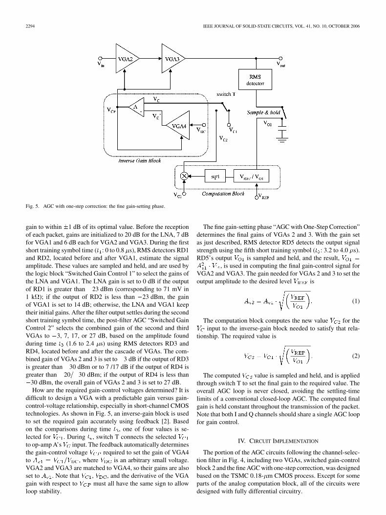
2294 IEEE JOURNAL OF SOLID-STATE CIRCUITS, VOL. 41, NO. 10, OCTOBER 2006
Fig. 5. AGC with one-step correction: the fine gain-setting phase.
gain to within 1 dB of its optimal value. Before the receptionof each packet, gains are initialized to 20 dB for the LNA, 7 dBfor VGA1 and 6 dB each for VGA2 and VGA3. During the firstshort training symbol time ( : 0 to 0.8 s), RMS detectors RD1and RD2, located before and after VGA1, estimate the signalamplitude. These values are sampled and held, and are used bythe logic block “Switched Gain Control 1” to select the gains ofthe LNA and VGA1. The LNA gain is set to 0 dB if the outputof RD1 is greater than 23 dBm (corresponding to 71 mV in1 k ); if the output of RD2 is less than 23 dBm, the gainof VGA1 is set to 14 dB; otherwise, the LNA and VGA1 keeptheir initial gains. After the filter output settles during the secondshort training symbol time, the post-filter AGC “Switched GainControl 2” selects the combined gain of the second and thirdVGAs to 3, 7, 17, or 27 dB, based on the amplitude foundduring time (1.6 to 2.4 s) using RMS detectors RD3 andRD4, located before and after the cascade of VGAs. The com-bined gain of VGAs 2 and 3 is set to 3 dB if the output of RD3is greater than 30 dBm or to 7 /17 dB if the output of RD4 isgreater than 20 30 dBm; if the output of RD4 is less than
30 dBm, the overall gain of VGAs 2 and 3 is set to 27 dB.How are the required gain-control voltages determined? It is
difficult to design a VGA with a predictable gain versus gain-control-voltage relationship, especially in short-channel CMOStechnologies. As shown in Fig. 5, an inverse-gain block is usedto set the required gain accurately using feedback [2]. Basedon the comparisons during time , one of four values is se-lected for . During , switch T connects the selectedto op-amp A’s input. The feedback automatically determinesthe gain-control voltage required to set the gain of VGA4to , where is an arbitrary small voltage.VGA2 and VGA3 are matched to VGA4, so their gains are alsoset to . Note that , , and the derivative of the VGAgain with respect to must all have the same sign to allowloop stability.
The fine gain-setting phase “AGC with One-Step Correction”determines the final gains of VGAs 2 and 3. With the gain setas just described, RMS detector RD5 detects the output signalstrength using the fifth short training symbol ( : 3.2 to 4.0 s).RD5’s output is sampled and held, and the result,
, is used in computing the final gain-control signal forVGA2 and VGA3. The gain needed for VGAs 2 and 3 to set theoutput amplitude to the desired level is
(1)
The computation block computes the new value for theinput to the inverse-gain block needed to satisfy that rela-
tionship. The required value is
(2)
The computed value is sampled and held, and is appliedthrough switch T to set the final gain to the required value. Theoverall AGC loop is never closed, avoiding the settling-timelimits of a conventional closed-loop AGC. The computed finalgain is held constant throughout the transmission of the packet.Note that both I and Q channels should share a single AGC loopfor gain control.
IV. CIRCUIT IMPLEMENTATION
The portion of the AGC circuits following the channel-selec-tion filter in Fig. 4, including two VGAs, switched gain-controlblock 2 and the fine AGC with one-step correction, was designedbased on the TSMC 0.18- m CMOS process. Except for someparts of the analog computation block, all of the circuits weredesigned with fully differential circuitry.

JEON et al.: ANALOG AGC CIRCUITRY FOR A CMOS WLAN RECEIVER 2295
Fig. 6. Schematic of (a) the proposed VGA and (b) the replica bias circuit.
A. Variable Gain Amplifier
The VGA must provide controllable gain, while maintaininggood linearity. However, because the inverse-gain block is used,the relationship of the gain-control voltage to the gain does notneed to follow any special form. To ensure linearity, the VGAuses a differential input circuit with transconductance Gm set bya fixed resistor. Cross-coupled differential pairs control the gainby steering a variable fraction of the signal to the differentialfixed-resistor load.
The VGA schematic is shown in Fig. 6(a). Differential inputis applied between the gates of source-
followers and , which are connected in feedback loopswith and to form a pair of so-called flipped voltage
followers (FVFs) [5]. The FVFs force constant current inand so that nodes and follow and withconstant offset. Thus, the current through fixed resistor
is accurately proportional to . The difference of currentsand is
(3)
where . and are passed to the transconductoroutput using current mirrors .
The voltages and on the gates of the dif-ferential pairs control how much of the transconductor currentpasses to the load. and are the outputs of a differen-tial difference amplifier (DDA), which uses common-mode feed-

2296 IEEE JOURNAL OF SOLID-STATE CIRCUITS, VOL. 41, NO. 10, OCTOBER 2006
Fig. 7. Schematic of the differential difference amplifier.
back (CMFB) to set the average of and to about 0.6 Vbelow the positive supply voltage, . The DDA circuit willbe described in more detail later. System operation ensures that
. For large , most of the signal cur-rent is passed to the differential load current , and the gain ap-proaches its maximum value, , where
. For small , the gain is nearly zero. In all cases,the common-mode (CM) current is constant at about
. The cascaded VGA stages are direct-coupled, so theoutput CM voltage must match the VGAs’ input CM range. Theload circuit uses level-shift resistors and to lower theCM output voltage to , typically about 0.5 V.The VGA circuit consumes total current of 1.5 mA.
Voltages in the VGA are highly constrained. If the input CMvoltage is too low, will go triode on signal peaks, and if it istoo high, will go triode. To maximize the input range, resis-tors and are placed in the feedback paths of the FVFsto shift the drain voltages of and closer to the negativesupply rail by . The situation is complicated further be-cause for constant , nodes X, Y and Z are all referred to ,which may vary 10% . To addressthis, current sources and are controlled by a voltage
that is generated by a replica bias circuit [Fig. 6(b)]. Thereplica circuit adjusts so that the drain voltages of and
in Fig. 6(a) equal the source voltage of , which is ref-erenced to ground rather than to . andvary with , so that node voltages and vary withwhile the voltages at nodes and are almost fixed, typi-cally about 0.65 V. The replica circuit has three feedback loops:two negative loops ( – – – – and – – )and a positive feedback loop – – – . The pres-ence of the positive feedback loop raises concerns that multipleoperating points may be possible [6], but detailed simulationsshowed that no undesired operating points exist.
The VGA structure shows good linearity with a large gainrange. However, tradeoffs were needed among gain range,
linearity, noise, bandwidth and current consumption. , ,and use near-minimum channels to enhance frequency re-sponse and linearity. The short channels increase flicker noise,so pMOS devices were chosen for these devices. Relativelylong transistors with relatively high were used forcurrent sources , , , , and . This enhancesmatching, output resistance and flicker noise. Channel widthswere chosen to optimize tradeoffs among noise and currentconsumption while meeting frequency response specifications.
B. DDA
The inverse-gain block used fully differential circuitsthroughout. Op-amp A in Fig. 5 was implemented using adifferential difference amplifier (DDA), as shown in Fig. 7.The DDA is the differential generalization of a single-ended opamp, with a pair of differential inputs, and differential outputwith CMFB [7]. The CMFB circuit uses source followersand and equal resistors and to average the outputs.
and also serve as level-shifters, producing a CM voltagereferenced to , as required for the control inputs ofthe VGA. The inverse-gain and CMFB loops are compensatedusing two grounded capacitors pF andseries-connected resistors . The DDAconsumes total current of 350 A.
C. RMS Detector
The RMS detector estimates the amplitude of the outputsignal, integrated over the duration of one short training symbol.(The circuit should perhaps be called a “pseudo-RMS” detector,because it does not implement the RMS function very accu-rately. Simulations showed that accurate RMS detection wasnot needed.) The dynamic range of the circuit is rather narrow,which is acceptable because the coarse gain-setting step ensuresthe signals are not far from their optimal value. As shown inFig. 8, the detector output voltage is storedas the difference of the ’s of a pair of diode-connected
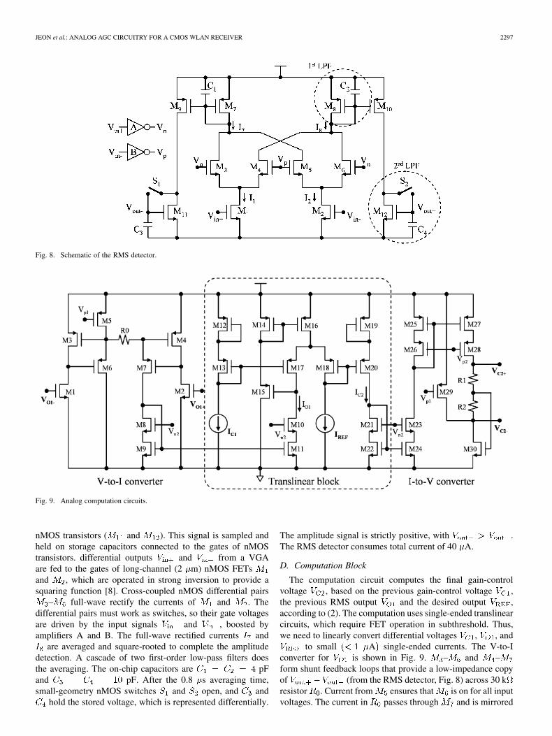
JEON et al.: ANALOG AGC CIRCUITRY FOR A CMOS WLAN RECEIVER 2297
Fig. 8. Schematic of the RMS detector.
Fig. 9. Analog computation circuits.
nMOS transistors ( and ). This signal is sampled andheld on storage capacitors connected to the gates of nMOStransistors. differential outputs and from a VGAare fed to the gates of long-channel (2 m) nMOS FETsand , which are operated in strong inversion to provide asquaring function [8]. Cross-coupled nMOS differential pairs
– full-wave rectify the currents of and . Thedifferential pairs must work as switches, so their gate voltagesare driven by the input signals and , boosted byamplifiers A and B. The full-wave rectified currents and
are averaged and square-rooted to complete the amplitudedetection. A cascade of two first-order low-pass filters doesthe averaging. The on-chip capacitors are pFand pF. After the 0.8 s averaging time,small-geometry nMOS switches and open, and and
hold the stored voltage, which is represented differentially.
The amplitude signal is strictly positive, with .The RMS detector consumes total current of 40 A.
D. Computation Block
The computation circuit computes the final gain-controlvoltage , based on the previous gain-control voltage ,the previous RMS output and the desired output ,according to (2). The computation uses single-ended translinearcircuits, which require FET operation in subthreshold. Thus,we need to linearly convert differential voltages , , and
to small A single-ended currents. The V-to-Iconverter for is shown in Fig. 9. – and –form shunt feedback loops that provide a low-impedance copyof (from the RMS detector, Fig. 8) across 30 kresistor . Current from ensures that is on for all inputvoltages. The current in passes through and is mirrored

2298 IEEE JOURNAL OF SOLID-STATE CIRCUITS, VOL. 41, NO. 10, OCTOBER 2006
Fig. 10. Die photo of the analog AGC circuitry.
Fig. 11. Gain control curve for the two-stage VGA. Ideally, the inverse-gaincircuit sets the gain of each VGA stage to VC/VDC.
by – , a 4:1 attenuating current mirror, to produce asmall linear current proportional to . Similar circuitsare used to produce and .
The analog computation is performed using transistors– . Applying the translinear principle [9] for FETs in
weak inversion yields
(4)
(5)
(6)
(7)
(8)
Fig. 12. Frequency response of the two-stage VGA.
The core transistors have large W/L to ensure weak inversionoperation with currents up to 1 A. , , andhave separate n-wells to avoid errors due to bulk effect.
The computed current is stepped up by 4:1 amplifyingcurrent mirrors – . The amplified output current flowsin equal-valued resistors and to produce the differentialoutput voltage between the top of and the bottom of
. The of sets the common-mode voltage, withsupplying common-mode current. The computation block con-sumes total current of 30 A.
E. Gain-Select Resistor Array and Other Circuits
The four selectable gains used in “Switched Gain ControlBlock 2”, plus the reference voltages , , and other keyvoltages are provided by an on-chip reference voltage generatorso that all gains are ultimately set by resistor ratios. The resistorsin the array use parallel and series combinations of unit resistorsto enhance matching [10].
Several other circuits were designed but are not describedhere for space reasons. These include the Gm-C filter, compara-tors and digital control circuits for switched-gain control, andon-chip bias-generation circuitry.
V. SIMULATION AND MEASUREMENT RESULTS
The post-filter AGC circuits described in Section IV werefabricated in the TSMC 0.18- m single-poly six-metal CMOSprocess available through MOSIS. The die photo is shown inFig. 10. The fabricated parts were packaged in a 40-pin ceramicDIP package.
The two-stage VGA was measured using sine-wave inputsignals from an Agilent 33120A. Output signals were mea-sured using an Agilent 54622D oscilloscope. Measurements ofthe gain-control function in Fig. 11 match simulation resultsclosely. Measured frequency responses of the two-stage VGAwith gains of 8, 12, and 32 dB gain are shown in Fig. 12.The results verify the circuit can pass the required bandwidthof 156.25 kHz to 8.3 MHz. The low-frequency response iscontrolled by the off-chip input coupling capacitor and theon-chip feedback resistor used to establish the operating point.Measurements showed that the VGA met these specificationsfor .
JEON et al.: ANALOG AGC CIRCUITRY FOR A CMOS WLAN RECEIVER 2299
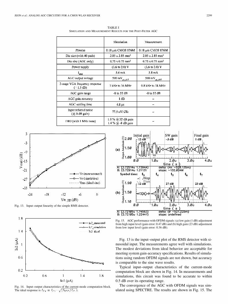
TABLE ISIMULATION AND MEASUREMENT RESULTS FOR THE POST-FILTER AGC
Fig. 13. Input–output linearity of the simple RMS detector.
Fig. 14. Input–output characteristics of the current-mode computation block.The ideal response is I = I � (I =I ).
Fig. 15. AGC performance with OFDM signals: (a) low gain (1 dB) adjustmentfrom high input level (gain error: 0.47 dB) and (b) high gain (23 dB) adjustmentfrom low input level (gain error: 0.36 dB).
Fig. 13 is the input–output plot of the RMS detector with si-nusoidal input. The measurements agree well with simulations.The modest deviations from ideal behavior are acceptable formeeting system gain-accuracy specifications. Results of simula-tions using random OFDM signals are not shown, but accuracyis comparable to the sine wave results.
Typical input–output characteristics of the current-modecomputation block are shown in Fig. 14. In measurements andsimulations, this circuit was found to be accurate to within0.5 dB over its operating range.
The convergence of the AGC with OFDM signals was sim-ulated using SPECTRE. The results are shown in Fig. 15. The
2300 IEEE JOURNAL OF SOLID-STATE CIRCUITS, VOL. 41, NO. 10, OCTOBER 2006
AGC uses symbol times through . The gain for the two-stage VGA was initialized to 12 dB. The switched gain is selectedduring and the final gain is adjusted during . The post-filterAGC adjusts signals to the desired level with gain error less than1 dB over the whole gain range. Table I summarizes the simu-lation and measurement results for the signal chain.
VI. CONCLUSION
Analog baseband AGC circuitry using a new open-loopanalog gain-control algorithm for an OFDM WLAN receiverhas been presented. The circuit detects signal strength from re-peated OFDM short training symbols and uses an inverse-gainfeedback technique with an open-loop computation for rapidyet accurate gain control. Newly designed fully differentiallinear VGAs, simple RMS detectors, and current-mode compu-tation circuitry are shown to be well-suited for use in OFDMAGC systems. The new AGC circuit needs just seven OFDMshort training symbols (5.6 s) to adjust the gain to the desiredlevel with gain error less than 1 dB.
REFERENCES
[1] Wireless Lan Medium Access Control (MAC) and Physical Layer(PHY) Specifications: High-Speed Physical Layer in the 5-GHz Band,IEEE Std. 802.11a, Part11, Sep. 1999.
[2] J. M. Khoury, “On the design of constant settling time AGC circuits,”IEEE Trans. Circuits Syst. II, Analog Digit. Signal Process., vol. 45,no. 3, pp. 283–294, Mar. 1998.
[3] O. Jeon, “Analog Baseband Processor for CMOS 5-GHz WLAN Re-ceiver,” Ph.D. dissertation, Univ. Florida, Gainesville, FL, 2005.
[4] M. Zargari, D. K. Su, C. P. Yue, S. Rabii, D. Weber, B. J. Kaczynski, S.S. Mehta, K. Singh, S. Mendis, and B. A. Wooley, “A 5-GHz CMOStransceiver for IEEE 802.11a wireless LAN system,” IEEE J. Solid-State Circuits, vol. 37, no. 12, pp. 1688–1694, Dec. 2002.
[5] R. G. Carvajal, J. Ramirez-Angulo, A. J. Lopez-Martin, A. Torralba,J. A. G. Galan, A. Carlosena, and F. M. Chavero, “The flipped voltagefollower: A useful cell for low-voltage low-power circuit design,” IEEETrans. Circuits Syst. I: Regular Papers, vol. 52, no. 7, pp. 1276–1291,Jul. 2005.
[6] R. M. Fox and M. Nagarajan, “Multiple operating points in a CMOSlog-domain filter,” IEEE Trans. Circuits Syst. II, Analog Digit. SignalProcess., vol. 46, no. 6, pp. 705–710, Jun. 1999.
[7] S. Huang, M. Ismail, and S. R. Zarabadi, “A wide range differentialdifference amplifier: A basic block for analog signal processing inMOS technology,” IEEE Trans. Circuits Syst. II, Analog Digit. SignalProcess., vol. 40, no. 5, pp. 289–301, May 1993.
[8] G. Han and E. Sanchez-Sinencio, “CMOS transconductance multi-pliers: A tutorial,” IEEE Trans. Circuits Syst. II, Analog Digit. SignalProcess., vol. 45, no. 12, pp. 1550–1563, Dec. 1998.
[9] B. Gilbert, C. Toumazou, D. G. Haigh, and F. J. Lidgey, “Current-mode circuits from a translinear viewpoint: A tutorial,” in Analogue ICDesign: The Current-Mode Approach (IEE Circuits and Systems Se-ries). London, U.K.: Peregrinus, 1993.
[10] C. Saint and J. Saint, IC Mask Design-Essential Layout Techniques.New York: McGraw Hill, 2002.
Okjune Jeon (M’04) received the B.S. degreein electronics engineering from Korea MilitaryAcademy, Seoul, Korea, in 1986, the M.S. degree inelectrical engineering from Case Western ReserveUniversity, Cleveland, OH, in 1990, and the Ph.D.degree in electrical engineering from the Universityof Florida, Gainesville, in 2005.
From 1997 to 2000, he was a faculty member of theDepartment of Electronics Engineering, Korea Mili-tary Academy. His research interests are analog andmixed-signal CMOS integrated circuits in wireless
LAN applications, including automatic gain control circuits, variable gain am-plifiers, and continuous time filters.
Robert M. Fox (M’78–SM’92) received the B.S. de-gree in physics from the University of Notre Dame,Notre Dame, IN, in 1972, and the M.S. and Ph.D. de-grees in electrical engineering from Auburn Univer-sity, Auburn, AL, in 1981 and 1986, respectively.
Since 1986, he has been on the Electrical andComputer Engineering faculty at the Universityof Florida, Gainesville, where he is an AssociateProfessor and Associate Department Chair. Hisresearch emphasizes circuit design and modelingfor advanced IC technologies. He has worked on a
variety of topics, including analog circuit design, cryogenic electronics, circuitdesign with SOI, radiation response of semiconductors, noise modeling, andmodeling of transistor self-heating. Currently, his research interests center ondesign-oriented analysis of analog integrated circuits, including low-voltagecircuit techniques, and analog and RF test strategies.
Dr. Fox is a member and former chair of the Analog Signal Processing Tech-nical Committee of the Circuits and System Society, and a member and formerchair of the Analog/Digital Circuits Technical Subcommittee for the Biplolar/BiCMOS Circuits and Technology Meeting (BCTM).
Brent A. Myers (M’96) received the B.S. degreefrom Purdue University, West Lafayette, IN, in 1979,the M.S. degree from Virginia Polytechnic Institute,Blacksburg, in 1982, and the Ph.D. degree from theFlorida Institute of Technology, Melbourne, in 1994,all in electrical engineering.
From 1979 to 1985, he worked at the MobileCommunications Division of General Electric,Lynchburg, VA, where he was involved in analogIC design for commercial and emergency mobilecommunication systems, and the AMPS cellular
system. In 1985, he joined Harris Semiconductor, Melbourne, FL, where he wasa Design Engineer for a wide variety of application-specific circuits, includingIR imaging networks, tape driver equalizers, and analog baseband processorsfor telecommunication and wireless systems. He is presently Director for RF,Mixed Signal, and Advance Development, at Conexant Systems, Melbourne,FL, where he is involved in circuit design for wireless LAN and high-speedwireline modems. He is an Adjunct Professor at the Florida Institute ofTechnology in the area of analog and mixed-signal design. He has eight patentsin the areas of signal processing and analog circuit techniques.