ICB1FL02G - Infineon Technologies
37
ICB1FL02G Smart Ballast Control IC for Fluorescent Lamp Ballasts Power Management & Supply Datasheet Version 2.1, September 2008
Transcript of ICB1FL02G - Infineon Technologies

ICB1FL02G
Smart Bal last Control IC for Fluorescent Lamp Bal lasts
P o w e r M a n a g e m e n t & S u p p l y
Datasheet Version 2.1, September 2008

Edition 2008-09Published by Infineon Technologies AG 81726 Munich, Germany© 10/16/08 Infineon Technologies AG All Rights Reserved.
Legal DisclaimerThe information given in this document shall in no event be regarded as a guarantee of conditions or characteristics. With respect to any examples or hints given herein, any typical values stated herein and/or any information regarding the application of the device, Infineon Technologies hereby disclaims any and all warranties and liabilities of any kind, including without limitation, warranties of non-infringement of intellectual property rights of any third party.
InformationFor further information on technology, delivery terms and conditions and prices, please contact the nearest Infineon Technologies Office (www.infineon.com).
WarningsDue to technical requirements, components may contain dangerous substances. For information on the types in question, please contact the nearest Infineon Technologies Office.Infineon Technologies components may be used in life-support devices or systems only with the express written approval of Infineon Technologies, if a failure of such components can reasonably be expected to cause the failure of that life-support device or system or to affect the safety or effectiveness of that device or system. Life support devices or systems are intended to be implanted in the human body or to support and/or maintain and sustain and/or protect human life. If they fail, it is reasonable to assume that the health of the user or other persons may be endangered.
ICB1FL02G Revision History: 2008-09 V 2.1
Previous Version: 2005-06-06 (ICB1FL01G)
Page Subjects (major changes since last revision)
19 Min Duration of EOL1
25 Preheating Time updated
26 EOL Current Threshold, AC & DC
Previous Version: 2006-02-08 (ICB1FL02G)
3 Package PG-DSO-18-2, halogen-free mould compound, WEEE compliant
11 Function removed and sentence deleted “During ignition and prerun mode the notch filter is bypassed.”
18 State diagram reworked (frequency range description corrected)
23 PFC zero current detector: clamping of positive voltages
24 PFC section: initial on-time and repetition time adapted
25 Inverter control: minimum duration of fault conditions EOL1, Cap Load 2 adapted
26 Restart after lamp removal: discharge resistor value adapted
33 LC equations corrected

Type Package
ICB1FL02G PG-DSO-18-2
ICB1FL02G
PG-DSO-18-1
Datasheet Version 2.1 3 September 2008
Product Highlights• Lowest Count of external Components• HV-Driver with coreless Transformer Technology• Improved Reliability and minimized Spread due to
digital and optimized analog control functions
Features PFC• Discontinuous Conduction Mode PFC• Integrated Compensation of PFC Control Loop• Adjustable PFC Current Limitation• Adjustable PFC Bus Voltage
Features Lamp Ballast Inverter• Supports Restart after Lamp Removal and End-of-
Life Detection in Multi-Lamp Topologies• End-of-Life (EOL) detected by adjustable
± Thresholds of sensed lamp voltage• Rectifier Effect detected by ratio of ± Amplitude of
Lamp Voltage• Detection of different capacitive Mode Operations• Adjustable Inverter Overcurrent Shutdown• Self-adaption of Ignition Time from 40ms to 235ms• Parameters adjustable by Resistors only• Pb-free lead plating; RoHS compliant• Halogen-free mould compound, WEEE compliant
Smart Ballast Control IC for Fluorescent Lamp Ballasts
DescriptionThe Smart Ballast IC is designed to control a Fluorescent Lamp Ballast including a Discontinuous Conduction Mode Power Factor Correction (PFC), a lamp Inverter Control and a High Voltage Level Shift Half-Bridge Driver.The application requires a minimum of external components. There are integrated low pass filters and an internal compensation for the PFC voltage loop control. Preheating time is adjustable by a single resistor only in the range between 0 and 2000ms. In the same way the preheating frequency and run frequency are set by resistors only. The control concept covers requirements for T5 lamp ballasts such as detection of end-of-life and detection of capacitive mode operation and other protection measures even in multilamp topologies. ICB1FL02G is easy to use and easy to design and therefore a basis for a cost effective solution for fluorescent lamp ballasts.
RF
RU
N
RF
PH
RT
PH
VC
C
PFCZCD
PFCGD
PFCVS
PFCCS
HSGD
HSVCC
HSGND
LSGD
LSCS
LVS
2
LVS
1
RE
S
GN
D
90 ... 270 V AC
ICB
1FL0
2GR
FR
UN
RF
PH
RT
PH
VC
C
PFCZCD
PFCGD
PFCVS
PFCCS
HSGD
HSVCC
HSGND
LSGD
LSCS
LVS
2
LVS
1
RE
S
GN
D
90 ... 270 V AC
ICB
1FL0
2G
PG-DSO-18-2
ICB1FL02G
Table of Contents Page
Datasheet Version 2.1 4 September 2008
1 Pin Configuration and Description . . . . . . . . . . . . . . . . . . . . . . . . . . . . . .51.1 Pin Configuration PG-DSO-18-1 . . . . . . . . . . . . . . . . . . . . . . . . . . . . . . . . . .51.2 Pin Description . . . . . . . . . . . . . . . . . . . . . . . . . . . . . . . . . . . . . . . . . . . . . . . .5
2 Block Diagram . . . . . . . . . . . . . . . . . . . . . . . . . . . . . . . . . . . . . . . . . . . . . . .8
3 Functional Description . . . . . . . . . . . . . . . . . . . . . . . . . . . . . . . . . . . . . . . .93.1 Typical operating levels during start-up . . . . . . . . . . . . . . . . . . . . . . . . . . . . .93.2 PFC Preconverter . . . . . . . . . . . . . . . . . . . . . . . . . . . . . . . . . . . . . . . . . . . .113.3 Typical operating levels during start-up . . . . . . . . . . . . . . . . . . . . . . . . . . . .133.4 Detection of End-of-Life and Rectifier Effect . . . . . . . . . . . . . . . . . . . . . . . .143.5 Detection of capacitive mode operating conditions . . . . . . . . . . . . . . . . . . .153.6 Interruption of Operation and Restart after Lamp Removal . . . . . . . . . . . . .16
4 State Diagram . . . . . . . . . . . . . . . . . . . . . . . . . . . . . . . . . . . . . . . . . . . . . . .18
5 Protection Functions . . . . . . . . . . . . . . . . . . . . . . . . . . . . . . . . . . . . . . . . .19
6 Electrical Characteristics . . . . . . . . . . . . . . . . . . . . . . . . . . . . . . . . . . . . .206.1 Absolute Maximum Ratings . . . . . . . . . . . . . . . . . . . . . . . . . . . . . . . . . . . . .206.2 Operating Range . . . . . . . . . . . . . . . . . . . . . . . . . . . . . . . . . . . . . . . . . . . . .216.3 Characteristics . . . . . . . . . . . . . . . . . . . . . . . . . . . . . . . . . . . . . . . . . . . . . . .226.3.1 Power Supply Section . . . . . . . . . . . . . . . . . . . . . . . . . . . . . . . . . . . . . . .226.3.2 PFC Section . . . . . . . . . . . . . . . . . . . . . . . . . . . . . . . . . . . . . . . . . . . . . . .236.3.2.1 PFC Current Sense (PFCCS) . . . . . . . . . . . . . . . . . . . . . . . . . . . . . . .236.3.2.2 PFC Zero Current Detector (PFCZCD) . . . . . . . . . . . . . . . . . . . . . . . .236.3.2.3 PFC Bus Voltage Sense (PFCVS) . . . . . . . . . . . . . . . . . . . . . . . . . . . .236.3.2.4 PFC PWM Generation . . . . . . . . . . . . . . . . . . . . . . . . . . . . . . . . . . . . .246.3.2.5 PFC Gate Drive (PFCGD) . . . . . . . . . . . . . . . . . . . . . . . . . . . . . . . . . .246.3.3 Inverter Section . . . . . . . . . . . . . . . . . . . . . . . . . . . . . . . . . . . . . . . . . . . .256.3.3.1 Inverter Control (RFRUN, RFPH, RTPH) . . . . . . . . . . . . . . . . . . . . . .256.3.3.2 Inverter Low Side Current Sense (LSCS) . . . . . . . . . . . . . . . . . . . . . .256.3.3.3 Restart after Lamp Removal (RES) . . . . . . . . . . . . . . . . . . . . . . . . . . .266.3.3.4 Lamp Voltage Sense (LVS1, LVS2) . . . . . . . . . . . . . . . . . . . . . . . . . .266.3.3.5 Inverter Low Side Gate Drive (LSGD) . . . . . . . . . . . . . . . . . . . . . . . . .276.3.3.6 Inverter High Side Gate Drive (HSGD) . . . . . . . . . . . . . . . . . . . . . . . .28
7 Application Examples . . . . . . . . . . . . . . . . . . . . . . . . . . . . . . . . . . . . . . . .297.1 Operating Behaviour of a Ballast for a single Fluorescent Lamp . . . . . . . . .297.2 Design Equations of a Ballast Application . . . . . . . . . . . . . . . . . . . . . . . . . .307.3 Multilamp Ballast Topologies . . . . . . . . . . . . . . . . . . . . . . . . . . . . . . . . . . . .35
8 Package Outlines . . . . . . . . . . . . . . . . . . . . . . . . . . . . . . . . . . . . . . . . . . . .36

ICB1FL02G
Pin Configuration and Description
1 Pin Configuration and Description1.1 Pin Configuration PG-DSO-18-1 1.2 Pin Description
LSCS (Low side current sense, Pin 1)This pin is directly connected to the shunt resistor which is located between the Source terminal of the low-side MOSFET of the inverter and ground.Internal clamping structures and filtering measures allow for sensing the Source current of the low-side inverter MOSFET without additional filter components. There is a first threshold of 0,8V, which provides a couple of increasing steps of frequency during ignition mode, if exceeded by the sensed current signal for a time longer than 250ns. If the sensed current signal exceeds a second threshold of 1,6V for longer than 400ns during all operating modes, a latched shut down of the IC will be the result.
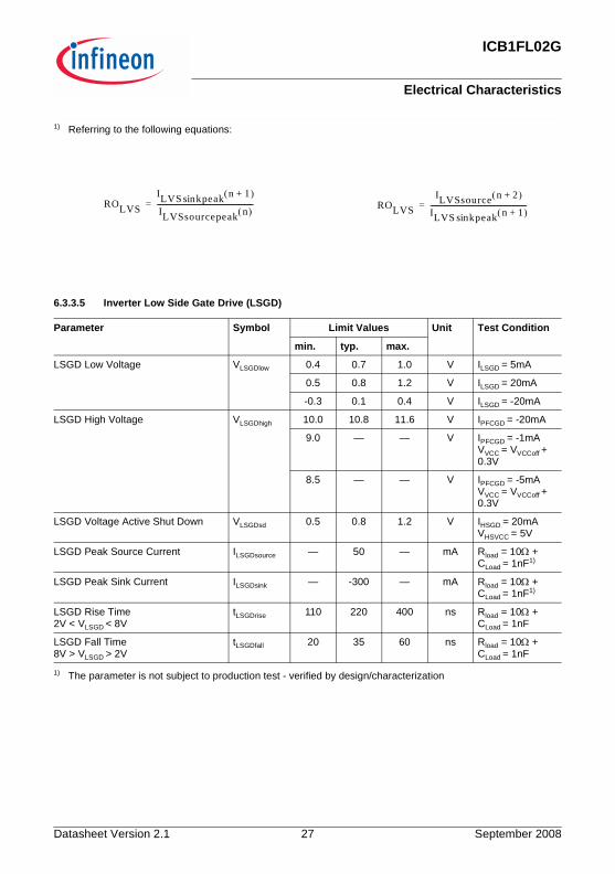
LSGD (Low side gate drive, Pin 2)The Gate of the low-side MOSFET in a half-bridge inverter topology is controlled by this pin. There is an active L-level during UVLO (undervoltage lockout) and a limitation of the max. H-level at 11V during normal operation. Turning on the MOSFET softly (with reduced diDRAIN/dt), the Gate drive voltage rises within 220ns from L-level to H-level. The fall time of the Gate drive voltage is less than 50ns in order to turn off quickly. This measure produces different switching speeds during turn-on and turn-off as it is usually achieved with a diode in parallel to a resistor in the Gate drive loop. It is recommended to use a resistor of about 15Ohm between drive pin and Gate in order to avoid oscillations and in order to shift the power dissipation of discharging the Gate capacitance into this resistor. The dead time between LSGD signal and HSGD signal is 1800ns typically.
VCC (Supply voltage, Pin 3)This pin provides the power supply of the ground related section of the IC. There is a turn-on threshold at 14V and an UVLO threshold at 10,5V. Upper supply voltage level is 17,5V. There is an internal zener diode clamping Vcc at 16V (2mA typically). The zener current is internally limited to 5mA max. For higher current levels an external zener diode is required. Current consumption during UVLO and during fault mode is less than 150µA. A ceramic capacitor close to the supply and GND pin is required in order to act as a low-impedance power source for Gate drive and logic signal currents.
GND (Ground, Pin 4)This pin is connected to ground and represents the ground level of the IC for supply voltage, Gate drive and sense signals.
Pin Symbol Function
1 LSCS Low side current sense (inverter)
2 LSGD Low side gate drive (inverter)
3 VCC Supply voltage
4 GND Controller ground
5 PFCGD PFC gate drive
6 PFCCS PFC current sense
7 PFCZCD PFC zero current detector
8 PFCVS PFC voltage sense
9 RFRUN Set R for run frequency
10 RFPH Set R for preheating frequency
11 RTPH Set R for preheating time
12 RES Restart after lamp removal
13 LVS1 Lamp voltage sense 1
14 LVS2 Lamp voltage sense 2
15 n.e. Not existing
16 n.e. Not existing
17 HSGND High side ground
18 HSVCC High side supply voltage
19 HSGD High side gate drive
20 HSGND High side ground
HSVCC
HSGND
RFPH
RES
LVS1
PG-DSO-18-2 (300mil)
LVS2
RFRUN
PFCVS
PFCZCD ICB
1FL0
2GGND
HSGDLSGD
PFCGD
LSCS
PFCCS
VCC
RTPH
HSGND
10
9
8
7
4
2
5
1
6
3
11
12
13
14
17
19
16
20
15
18
Datasheet Version 2.1 5 September 2008

ICB1FL02G
Pin Configuration and Description
PFCGD (PFC gate drive, Pin 5)The Gate of the MOSFET in the PFC preconverter designed in boost topology is controlled by this pin. There is an active L-level during UVLO and a limitation of the max. H-level at 11V during normal operation. Turning on the MOSFET softly (with a reduced diDRAIN/dt), the Gate drive voltage rises within 220ns from L-level to H-level. The fall time of the Gate voltage is less than 50ns in order to turn off quickly. A resistor of about 10Ohm between drive pin and Gate in order to avoid oscillations and in order to shift the power dissipation of discharging the Gate capacitance into this resistor is recommended. The PFC section of the IC controls a boost converter as a PFC preconverter in discontinuous conduction mode (DCM). Typically the control starts with Gate drive pulses with an on-time of 1µs increasing up to 24µs and a off-time of 40µs. As soon as a sufficient ZCD (zero current detector) signal is available, the operating mode changes from a fixed frequent operation to an operation with variable frequency. During rated and medium load conditions we get an operation with critical conduction mode (CritCM), that means triangular shaped currents in the boost converter choke without gaps when reaching the zero level and variable operating frequency. During light load (detected by the internal error amplifier) we get an operation with discontinuous conduction mode (DCM), that means triangular shaped currents in the boost converter choke with gaps when reaching the zero level and variable operating frequency in order to avoid steps in the consumed line current.
PFCCS (PFC current sense, Pin 6)The voltage drop across a shunt resistor located between Source of the PFC MOSFET and GND is sensed with this pin. If the level exceeds a threshold of 1V for longer than 260ns the PFC Gate drive is turned off as long as the ZCD (zero current detector) enables a new cycle. If there is no ZCD signal available within 40µs after turn-off of the PFC Gate drive, a new cycle is initiated from an internal start-up timer.
PFCZCD (PFC zero current detection, Pin 7)This pin senses the point of time when the current through the boost inductor becomes zero during off-time of the PFC MOSFET in order to initiate a new cycle. The moment of interest appears when the voltage of the separate ZCD winding changes from positive to negative level which represents a voltage of zero at the inductor windings and therefore the end of current flow from lower input voltage level to higher output voltage level. There is a threshold with hysteresis, for increasing voltage a level of 1,5V, for decreasing voltage a level of 0,5V, that detects the change of inductor voltage. A resistor connected between ZCD winding and sense input limits the sink
and source current of the sense pin, when the voltage of the ZCD winding exceeds the internal clamping levels (6,3V and -2,9V @ 4mA) of the IC.If the sensed level of the ZCD winding is not sufficient (e.g. during start-up), an internal start-up timer will initiate a new cycle every 40µs after turn-off of the PFC Gate drive.
PFCVS (PFC voltage sense, Pin 8)The intermediate circuit voltage (bus voltage) at the smoothing capacitor is sensed by a resistive divider at this pin. The internal reference voltage for rated bus voltage is 2,5V. There are further thresholds at 0,375V (15% of rated bus voltage), 1,83V (73% of rated bus voltage) and 2,725V (109% of rated bus voltage) for detecting open control loop, undervoltage and overvoltage.
RFRUN (Set R for run frequency, Pin 9)A resistor from this pin to ground sets the operating frequency of the inverter during run mode. Typical run frequency range is 20kHz to 100kHz. The set resistor RRFRUN can be calculated based on the run frequency fRUN according to the equation
RFPH (Set R for preheating frequency, Pin 10)A resistor from this pin to ground sets together with the resistor at pin 9 the operating frequency of the inverter during preheat mode. Typical preheat frequency range is run frequency (as a minimum) to 150kHz. The set resistor RRFPH can be calculated based on the preheat frequency fPH and the resistor RRFRUN according to the equation:
The total value of both resistors RRFPH and RRFRUNswitched in parallel should not be less than 3,3kOhm.
RTPH (Set R for preheating time, Pin 11)A resistor from this pin to ground sets the preheating time of the inverter during preheat mode. A set resistor range from zero to 18kOhm corresponds to a range of preheating time from zero to 2000ms subdivided in 127 steps.
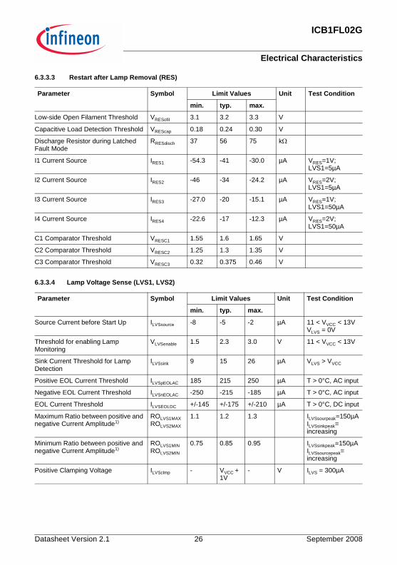
RES (Restart after lamp removal, Pin 12)A source current out of this pin via resistor and filament to ground monitors the existence of the low-side filament of the fluorescent lamp for restart after lamp
RRFRUN5 108
ΩHz⋅fRUN
-----------------------------=
RRFPHRRFRUN
fPH RRFRUN⋅
5 108ΩHz⋅
---------------------------------------- 1–
--------------------------------------------------=
Datasheet Version 2.1 6 September 2008

ICB1FL02G
Pin Configuration and Description
removal. A capacitor from this pin directly to ground eliminates a superimposed AC voltage that is generated as a voltage drop across the low-side filament. With a second sense resistor the filament of a paralleled lamp can be included into the lamp removal sense. During typical start-up with connected filaments of the lamp a current source IRES3 (20µA) is active as long as Vcc> 10,5V and VRES< VRESC1 (1,6V). An open Low-side filament is detected, when VRES> VRESC1. Such a condition will prevent the start-up of the IC. In addition the comparator threshold is set to VRESC2 (1,3V) and the current source changes to IRES4 (17µA). Now the system is waiting for a voltage level lower than VRESC2at the RES-Pin that indicates a connected low-side filament, which will enable the start-up of the IC.An open high-side filament is detected when there is no sink current ILVSsink (15µA) into both of the LVS-Pins before the VCC start-up threshold is reached. Under these conditions the current source at the RES-Pin is IRES1 (41µA) as long as Vcc> 10,5V and VRES< VRESC1(1,6V) and the current source is IRES2 (34µA) when the threshold has changed to VRESC2 (1,3V). In this way the detection of the high-side filament is mirrored to the levels on the RES-Pin. Finally there is a delay function implemented at the RES-Pin. When a fault condition happens e.g. by an end-of-life criteria the inverter is turned-off. In some topologies a transient AC lamp voltage may occur immediately after shut down of the Gate drives which could be interpreted as a lamp removal. In order to generate a delay for the detection of a lamp removal the capacitor at the RES-Pin is charged by the IRES3(20µA) current source up to the threshold VRESC1 (1,6V) and discharged by an internal resistor RRESdisch , which operates in parallel to the external sense resistor at this pin, to the threshold VRESC3 (0,375V). The total delay amounts to 32 of these cycles, which corresponds to a delay time between 30ms to 100ms dependent on capacitor value. In addition this pin is applied to sense capacitive mode operation by use of a further capacitor connected from this pin to the nod of the high-side MOSFET’s Source terminal and the low-side MOSFET’s Drain terminal. The sense capacitor and the filter capacitor are acting as a capacitive voltage divider that allows for detecting voltage slopes versus timing sequence and therefore indicating capacitive mode operation. A typical ratio of the capacitive divider is 410V/2,2V which results in the capacitor values e.g. of 10nF and 53pF (56pF).
LVS1 (Lamp voltage sense 1, Pin 13)Before the IC enters the softstart mode this pin has to sense a sink current above 26µA (max) which is fed via resistors from the bus voltage across the high-side filament of the fluorescent lamp in order to monitor the existence of the filament for restart after lamp removal. Together with LVS2 (pin 14) and RES (pin 12) the IC can monitor the lamp removal of totally 4 lamps.
During run mode the lamp voltage is sensed by the AC current fed into this pin via resistors. Exceeding one of the two thresholds of either +215µA or -215µA cycle by cycle for longer than 610µs, the interpretation of this event is a failure due to EOL1 (end-of-life). A rectifier effect (EOL2) is assumed if the ratio of the sequence of positive and negative amplitudes is above 1,15 or below 0,85 for longer than 500ms. A failure due to EOL1 or EOL2 changes the operating mode from run mode into a latched fault mode that stops the operation until a reset occurs by lamp removal or by cycle of power. EOL1 and EOL2 require an AC current with zerocrossings at LVS-Pin for a reliable detection. A DC current at LVS-Pin results in a definite turn-off action acc. to EOL1 only if the sensed current exceeds the threshold ILVSEOLDC= +/-175µA (typically).If the functionality of this pin is not required (e.g. for single lamp designs) it can be disabled by connecting this pin to ground.
LVS2 (Lamp voltage sense 2, Pin 14)Same functionality as LVS1 (pin 13) for monitoring a paralleled lamp circuit.
HSGND (High side ground, Pin 17)This pin is connected to the Source terminal of the high-side MOSFET, which is also the nod of high-side and low-side MOSFET. This pin represents the floating ground level of the high-side driver and high-side supply.
HSVCC (High side supply voltage, Pin 18)This pin provides the power supply of the high-side ground related section of the IC. An external capacitor between pin 15 and 16 acts like a floating battery which has to be recharged cycle by cycle via high voltage diode from low-side supply voltage during on-time of the low-side MOSFET. There is an UVLO threshold with hysteresis that enables high-side section at 10,1V and disables it at 8,4V.
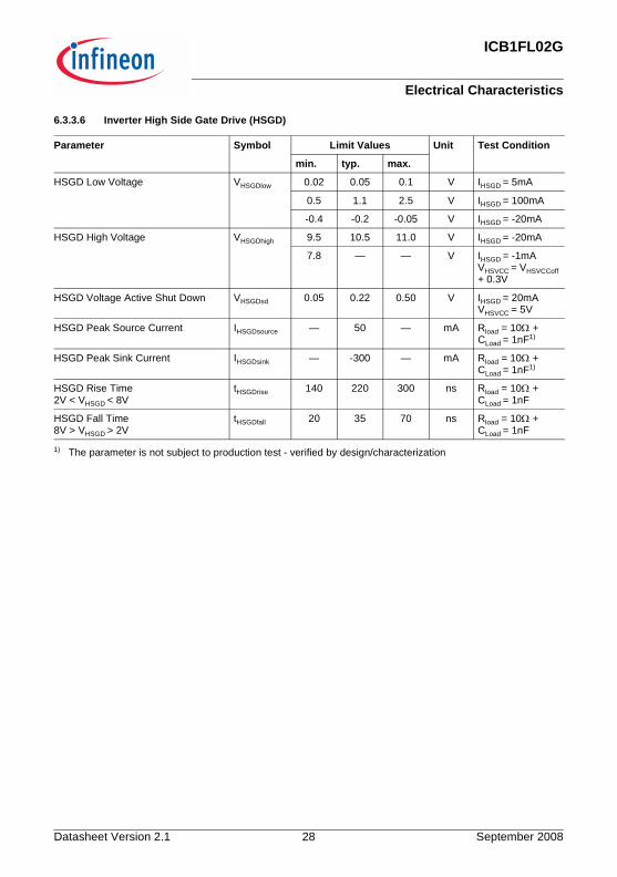
HSGD (High side gate drive, Pin 19)The Gate of the high-side MOSFET in a half-bridge inverter topology is controlled by this pin. There is an active L-level during UVLO and a limitation of the max. H-level at 11V during normal operation. The switching characteristics are the same as described for LSGD (pin 2). It is recommended to use a resistor of about 15Ohm between drive pin and Gate in order to avoid oscillations and in order to shift the power dissipation of discharging the Gate capacitance into this resistor. The dead time between LSGD signal and HSGD signal is 1800ns typically.
HSGND (High side ground, Pin 20)This pin is internally connected with pin 17.
Datasheet Version 2.1 7 September 2008

ICB1FL02G
Block Diagram
2 Block Diagram
Figure 1 Simplified Blockdiagram of ICB1FL02G
9RF
RUN
8PF
CVS
10RF
PH
11RT
PH
Int.
Sup
ply
& G3
Z1 16V
@2m
A
VCC
5V
5µs
Bla
nkU
VLO
V TH1=
14,0
VV TH
2=10
,5V
C2
V TH=1
0,5V
OFF
_H
VD
D_g
ood_
H
C1
POW
ERSU
PPLY
S1
R1
RTP
HC
1
T1T2
PH
END
_H
5,0V
dac7
2,0V
Softs
tart
and
Preh
eat M
ode
Oth
er M
odes
OP
Bias
Cel
l15µ
sB
lank
PREH
EAT_
TIM
ER
Osc
illato
r
I osc!
f osc
S3S1
R1
OSC
vref
RFP
H
RFR
UN
T1T2
I OSC
2,5V
Preh
eat M
ode
Oth
er M
odes
Oth
er M
odes
Run
Mod
e
dac7
, dac
4 =
GN
D d
urin
gru
n m
ode,
othe
rwis
etra
nsie
ntvo
ltage
leve
ls(0
..2,5
V)
5,0V
dac7
dac4
VCO
2,5V
dac7
OP
Bia
s C
ell1
OP
Bia
s C
ell2
OP
Bia
s C
ell3
S2
VCC
OP
1 R1
A v= 2
.5
R2
V REF
= 2,
50V
8-Bi
t AD
C
C1
VTH
1= 2
,725
VV
TH2=
2,6
25V
C2
V TH=
1,83
V
C3
V TH=
0,37
5V
VBU
SO
VER
VOLT
AGE
VBU
SU
ND
ERVO
LTAG
E
VBU
S O
PEN
LOO
P D
ETEC
T
DIG
ITAL
LO
OP
CO
NTR
OL
PFC
_PW
M_I
N
5µs
Bla
nk
5µs
Bla
nk
5µs
Bla
nk
PFC
_VS
END
-OF-
LIFE
2LV
S2
14LV
S2LV
S_2
SPI
for
Test
Mod
e
Band
gap
Vref
=2.5
V
Mas
ter
Cloc
k
Digi
tal
sequ
entia
lco
ntro
l
dac4
dac7
DS
C
OS
C
PH
END
_H
MC
LOC
K_SP
IP
OW
ER
_DO
WN
_L
D1
PFC
CS
C1
1.0V
260n
sB
lank
C2
V TH1=
1,5V
V TH2=
0,5V
D2
R1
R2
D35,
0V
PFC
_ZC
D
PFC_
CLI
M
6PF
CCS
7PF
CZCD
D1
Star
t-up
timer
off-t
ime
40µs
PFC
PWM
&C
ontro
l
PFC
PWM
PFC
_PW
M_I
N
PFC
GD
IN
DS
C
PFC
GD
Z1
1
G1
T2 T1
D2 D1
VCC
PFC
GD
IN
5PF
CGD
slop
e co
ntro
lZ1 =12V
022
0ns
t
VG
ATE
1,8µ
sD
ead
time
PWM
inve
rter
INVP
WM
DS
C
LS HS
C1 C2
0,8V
1,6V
250n
sBl
ank
400n
sBl
ank
INV
_OC
IGN
-LIM
INVC
LIM
1LS
CS
2LS
GD
3 4G
ND
LSG
D
Z1
1
G1
T2 T1
D2
D1
VCC
LS
slop
e co
ntro
lZ1 =12V
022
0ns
t
VG
ATE
HSG
D
Z1
1
G1
D2
D1
T1T2
HSVC
C
1918 17
HSG
D
HSG
ND
slop
e co
ntro
lZ1 =1
2V
022
0ns
t
V GAT
E
HS
Cor
eles
s T.
& G6
C3
C4
D2
D1 VC
C
5V
EN
D-O
F-LI
FE 1
DQ
& G2
EN
I1 =
5µA
PO
WE
R_D
OW
N_L
H =
on
L =
off
EO
LOFF
_L
EO
LAC
TIV
E_H
LIN
SER
T_H
G3
EN=L
=>
Stat
us L
atch
ed
+215
µA
-215
µA
1G
5C
1
15µA
C2
2,0V
D3
1G
1
1G
4
I LVS
LVS
1
13LV
S1
> 1,
15...
......
=> Q
= H
= 0,
85..1
,15=
> Q
= L
< 0,
85…
.....=
> Q
= H Q
OFF
_H
V PEA
K(N+
1)
V PEA
K(N)
=
LVS_
1
T1
N
I LVS
Pea
k R
ectif
icat
ion
N+2
N+1V
PEAK
(N+1
)
V PEAK
(N)
END
-OF-
LIFE
2C
APAC
ITIV
E LO
AD 1
OPE
N F
ILAM
ENT
VBU
S O
VER
VOLT
AGE
INVE
RTE
RO
VER
CU
RR
ENT
Up
& D
own
Cou
nter
min
.dur
atio
nof
effe
ct:
500m
s
END
-OF-
LIFE
1C
APAC
ITIV
E LO
AD 2
OPE
RAT
ION
ABO
VER
UN
FR
EQU
ENC
Y
1
ERR
OR
_LO
GIC
min
.dur
atio
n of
effe
ct:
400n
smin
.dur
atio
nof
effe
ct:
610µ
s
235m
saf
ter e
nd o
f pre
heat
mod
e
1
RS
FAUL
TLA
TCH 1
PO
WE
R_D
OW
N_L
LVS
1_L
LVS
2_L
OFF
_HLA
MP
_INS
ER
T_H
UVLO
_LO
PE
N_L
OO
P_L
&
1
1
0,37
5V
1,3V
1,6V
5,0V
T1
3,2V
0,24
V
INV
1
T1
DQ
DQ
G1
DQ
G2
G3
12RE
S5µ
sB
lank
5µs
Bla
nk
5µs
Bla
nk
I3=
20µA
; V R
ES<
1,6V
; VC
C> 1
0,5V
; ILV
S>
15µA
; or d
urin
g ru
n m
ode
I1=
41µA
; V R
ES<
1,6V
; VC
C> 1
0,5V
; ILV
S<
15µA
;I4
= 17
µA;
V RES
> 1,
6V; V
CC>
10,
5V; I
LVS>
15µA
;I2
= 34
µA;
V RES
> 1,
6V; V
CC>
10,
5V; I
LVS<
15µA
;I5
= 41
µA &
0µA
alte
rnat
ing
for 3
2 cy
cles
as
a de
lay;
V DSCap
aciti
ve L
oad
Det
ectio
n
CAP
LO
AD1
V DS
CAP
LO
AD2
CAP
LOAD
-RES
Lam
p in
sert
dete
ctio
n fo
rVR
ES <
1,6
Vdu
ring
pow
er d
own.
Del
ay g
ener
ator
for a
ctiv
atin
gla
mp
rem
oval
afte
r fau
lt la
tch
is s
et.
LSG
DIN
_HH
SGD
IN_H
CA
PLO
AD
1
CA
PLO
AD
2
OPE
N_F
ILA
ME
NT
LVS
2LV
S1
LAM
P_I
NSE
RT_
H
&
C1
C4
C3
C5
C2
54k
Datasheet Version 2.1 8 September 2008

ICB1FL02G
Functional Description
3 Functional Description3.1 Typical operating levels during start-upThe control of the ballast should be able to start the operation within less than 100ms. Therefore the current consumption of the IC is less than 150µA during UVLO. With a small start-up capacitor (about 1µF) and a power supply, that feeds within 100µs (charge pump of the inverter) the IC can cover this feature.As long as the Vcc is less than 10,5V, the current consumption is typically 80µA. Above a Vcc voltage level of 10,5V the IC checks whether the lamp(s) are assembled by detecting a current across the filaments. The low-side filament is checked from a source current (20µA typ.) out of pin RES, that produces a voltage drop at the sense resistor, which is connected via low-side filament to ground. An open filament is detected, when the voltage level at pin RES is above 1,6V. The high-side filament (or the high-side of a series topology) is checked by a current (15µA typ.) into the LVS pin. An open high-side filament causes a higher source current (41µA / 34µA typ.) out of pin RES in order to exceed the 1,6V threshold. If one of both filaments is not able to conduct the test current, the control circuit is disabled. The IC is enabled as soon as a sufficient current is detected across the filaments or the supply voltage drops below the UVLO threshold (10,5V) e.g. by turn-off and turn-on of mains switch.
Figure 2 Progress of levels during a typical start-up.
When the previous conditions are fulfilled, and Vcc has reached the start-up threshold (14V), there is finally a check of the Bus voltage. If the level is less than 15% of rated Bus voltage, the IC is waiting in power down mode until the voltage increases. If the level is above 109% of rated Bus voltage there is no Gate drive, but an active IC. The supply voltage Vcc will fall below the UVLO threshold and a new start-up attempt is initiated.As soon as start-up conditions are fulfilled the IC starts driving the inverter with the start-up frequency of 125kHz. Now the complete control including timers and the PFC control can be set in action. There are current limitation thresholds for PFC preconverter and ballast inverter equipped with spike filters. The PFC current limitation interrupts the on-time of the PFC MOSFET if the voltage drop at shunt resistor exceeds 1V and restarts after next input from ZCD. The inverter current limitation operates with a first threshold of 0,8V which increases the operating frequency during ignition mode if exceeded. A second threshold is provided at 1,6V that stops the whole control circuit and latches this event as a fault.
VCC
14,0V
10,5V
IVCC
80µA5mA+ QGate
VRES
1,6V
IRES
20µA
ILVS
>15µA
< +/- 2,5mA
3,2V
UVLOSTART-UPHYSTERESIS
IC ACTIVESOFTSTART
t
t
t
t
t
<150µA80µA
<3,2V
20µA
>15µA
Datasheet Version 2.1 9 September 2008

ICB1FL02G
Functional Description
Figure 3 Start-up with LS filament broken and subsequent lamp removal.
Figure 4 Start-up with HS filament broken and subsequent lamp removal.
VCC
14,0V
10,5V
IVCC
80µA5mA+ QGate
VRES
1,6V
IRES
20µA
ILVS
>15µA
3,2V
UVLOSTART-UPHYSTERESIS
IC ACTIVESOFTSTART
t
t
t
t
t< +/- 2,5mA
17µA 34µA 17µA 20µA
16,0V
LS FILAMENT OPENHS FILAMENT CLOSED
LAMP REMOVALLS + HS OPEN
1,3V
POWERDOWNSIGNAL
t
20µA
5,0V
H
VRES> 1,3V
80µA <170µA
>15µA >15µA
<3,2V
<150µA
VCC
14,0V
10,5V
IVCC
80µA5mA+ QGate
VRES
1,6V
IRES
20µA
ILVS
>15µA
3,2V
UVLOIC ACTIVESOFTSTART
t
t
t
t
t< +/- 2,5mA
34µA 34µA 17µA 20µA
16,0V
LAMP REMOVALLS + HS OPEN
VRES> 1,3V
1,3V
POWERDOWNSIGNAL
t
41µA
5,0V
H
<3,2V
<170µA80µA
START-UPHYSTERESIS
HS FILAMENT OPENLS FILAMENT CLOSED
>15µA
1,3V
<150µA
Datasheet Version 2.1 10 September 2008

ICB1FL02G
Functional Description
3.2 PFC PreconverterPFC is starting with a fixed frequent operation (ca. 25kHz), beginning with an on-time of 1µs and an off-time of 40µs. The on-time is enlarged every 400µs to a maximum on-time of 23µs. The control switches over into critical conduction mode (CritCM) operation as soon as a sufficient ZCD signal is available. There is an overvoltage threshold at 109% of rated Bus voltage that stops PFC Gate drive as long as the Bus voltage has reached a level of 105% of rated Bus voltage again. The compensation of the voltage control loop is completely integrated. The internal reference level of the Bus voltage sense (PFCVS) is 2,5V with high accuracy.The PFC control operates in CritCM in the range of 23µs > on-time > 2,3µs. For lower loads the control operates in discontinuous conduction mode (DCM) with an on-time down to 0,5µs and an increasing off-time. With this control method the PFC preconverter covers a stable operation from 100% of load to 0,1% .
Figure 5 Circuit Diagram of the PFC preconverter section.
Overvoltage, undervoltage and open loop detection at pin PFCVS are sensed by analog comparators. The BUS voltage loop control is provided by a 8bit sigma-delta A/D-Converter with a sampling rate of 400µs and a resolution of 4mV/bit. So a range of +/- 0,5V from the reference level of 2,50V is covered. The digital error signal has to pass a digital notch filter in order to suppress the AC voltage ripple of twice of the mains frequency. A subsequent error amplifier with PI characteristic cares for stable operation of the PFC preconverter.The zero current detection is sensed by a separate pin PFCZCD. The information of finished current flow during demagnetization is required in CritCM and in DCM as well. The input is equipped with a special filtering including a blanking of typically 500ns and is combined with a large hysteresis between the thresholds of typically 0,5V and 1,5V. In case of bad coupling between primary inductor winding and secondary ZCD-winding an additional filtering by a capacitor at ZCD pin might be necessary in order to avoid mistriggering by long lasting oscillations during switching slopes of the PFC MOSFET.
Figure 6 Structure of the mixed digital and analog control of PFC preconverter.
RF
RU
N
RF
PH
RT
PH
VC
C
PFCZCD
PFCGD
PFCVS
PFCCS
HSGD
HSVCC
HSGND
LSGD
LSCS
LVS
2
LVS
1
RE
S
GN
D
90 ...270 VAC
ICB
1FL0
2GR1
R2
D1...4
LRFI
L1 D5
Q1R8
R7
R3
R4
R6D9
C1 C2
C3 R9
R5 R12 R13C7
VBUS
Vcc
PFCVS PFCGD
PFCCS
PFCZCD
Pulse widthGenerator
GateDriver
OvercurrentProtection1,0V +/-5%
ZCD1,50V / 0,5V
Start-up
Clock600kHz
PI LoopControl
NotchFilter
Undervoltage73% +/- 2,5%
Overvoltage109% +/-2,0%
Open LoopDetection
15% +/- 20%
Σ∆-ADCSRate 400µsRes 4mV/bit
Reference2,50V
+/-1,5%
Datasheet Version 2.1 11 September 2008
ICB1FL02G
Functional Description
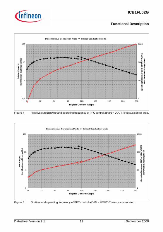
Figure 7 Relative output power and operating frequency of PFC control at VIN = VOUT /2 versus control step.
Figure 8 On-time and operating frequency of PFC control at VIN = VOUT /2 versus control step.
Discontinuous Conduction Mode <> Critical Conduction Mode
0,1
1
10
100
0 32 64 96 128 160 192 224 256
Digital Control Steps
Rel
ativ
e Po
wer
%id
entif
icat
ion
mar
king
s un
fille
d
1
10
100
1000
Ope
ratin
g Fr
eque
ncy
(kH
z) a
t VIN
= V
OU
T/2
iden
tific
atio
n m
arki
ngs
fille
d
Discontinuous Conduction Mode <> Critical Conduction Mode
0
1
10
100
0 32 64 96 128 160 192 224 256
Digital Control Steps
On-
Tim
e (µ
s)id
entif
icat
ion
mar
king
s un
fille
d
1
10
100
1000
Ope
ratin
g Fr
eque
ncy
(kHz
) at V
IN =
VO
UT/2
iden
tific
atio
n m
arki
ngs
fille
d
Datasheet Version 2.1 12 September 2008
ICB1FL02G
Functional Description
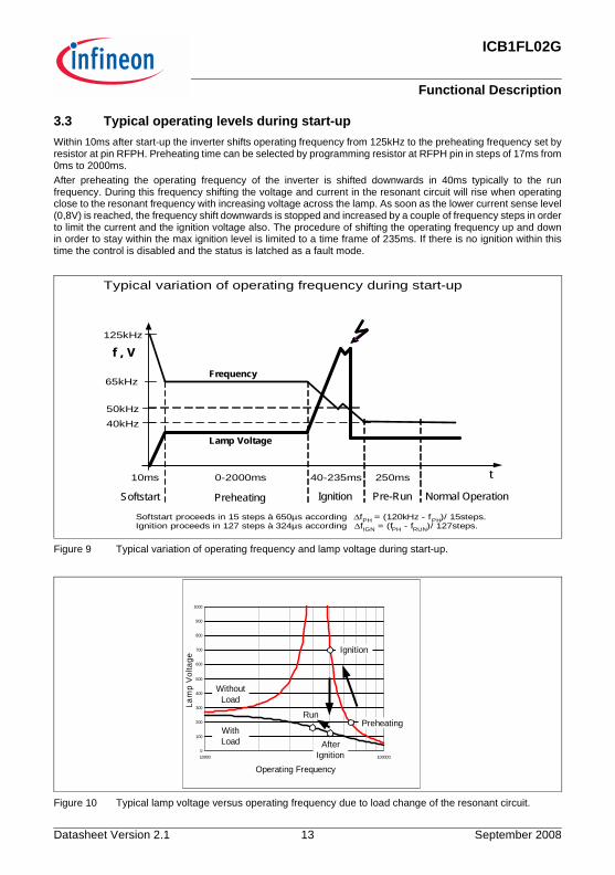
3.3 Typical operating levels during start-upWithin 10ms after start-up the inverter shifts operating frequency from 125kHz to the preheating frequency set by resistor at pin RFPH. Preheating time can be selected by programming resistor at RFPH pin in steps of 17ms from 0ms to 2000ms. After preheating the operating frequency of the inverter is shifted downwards in 40ms typically to the run frequency. During this frequency shifting the voltage and current in the resonant circuit will rise when operating close to the resonant frequency with increasing voltage across the lamp. As soon as the lower current sense level (0,8V) is reached, the frequency shift downwards is stopped and increased by a couple of frequency steps in order to limit the current and the ignition voltage also. The procedure of shifting the operating frequency up and down in order to stay within the max ignition level is limited to a time frame of 235ms. If there is no ignition within this time the control is disabled and the status is latched as a fault mode.
Figure 9 Typical variation of operating frequency and lamp voltage during start-up.
Figure 10 Typical lamp voltage versus operating frequency due to load change of the resonant circuit.
65kHz
50kHz40kHz
Preheating Ignition Normal Operation
125kHz
Softstart
Frequency
f , V
Lamp Voltage
40-235ms t10ms 0-2000ms
Pre-Run
250ms
Typical variation of operating frequency during start-up
Softstart proceeds in 15 steps à 650µs according ∆fPH = (120kHz - fPH)/ 15steps.Ignition proceeds in 127 steps à 324µs according ∆fIGN = (fPH - fRUN)/ 127steps.
0
100
200
300
400
500
600
700
800
900
1000
10000 100000
Operating Frequency
Lam
p V
olta
ge
Ignition
Preheating
AfterIgnition
Run
WithoutLoad
WithLoad
Datasheet Version 2.1 13 September 2008

ICB1FL02G
Functional Description
3.4 Detection of End-of-Life and Rectifier EffectAfter ignition the lamp voltage breaks down to its run voltage level (typically 50Vpeak to 300Vpeak). Reaching the run frequency there follows a time period of 250ms called Pre-Run Mode, in which some of the monitoring features (EOL1, EOL2, Cap.Load1) are still disabled. In the subsequent Run Mode the End-of-life (EOL) monitoring is enabled. The event EOL1 is detected by measuring the positive and negative peak level of the lamp voltage by a current fed into the LVS pin (R17, R18,R19 in Fig. 11). If the sensed current exceeds 215µA for longer than 610µs the status end-of-life (EOL1) or the exceeding of the maximum output power is detected. In Fig. 12 the different levels of the sensed lamp voltage are illustrated.
Figure 11 Circuit diagram of the lamp inverter section.
Figure 12 Sensed lamp voltage levels.
RF
RU
N
RF
PH
RT
PH
VC
C
PFCZCD
PFCGD
PFCVS
PFCCS
HSGD
HSVCC
HSGND
LSGD
LSCS
LVS
2
LVS
1
RE
S
GN
D
ICB
1FL0
2G
VBUS
Vcc
D9
C2
R5 R12 R13
R10
R11
C4
C7
Q2
Q3
R14
R16R15
R17 R18 R19
R20
C5
C6 C8
C9
C10
L2
D6D7
D8R30 D10
t
+ Shut down level
- Shut down level
- Ignition level
+ Ignition level
+ EOL Threshold
- EOL Threshold
IVL+PEAKI/IVL-PEAKI
VLAMP-RUN
VLAMP-IGN
0
Datasheet Version 2.1 14 September 2008
ICB1FL02G
Functional Description
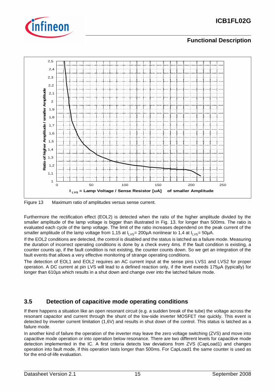
Figure 13 Maximum ratio of amplitudes versus sense current.
Furthermore the rectification effect (EOL2) is detected when the ratio of the higher amplitude divided by the smaller amplitude of the lamp voltage is bigger than illustrated in Fig. 13. for longer than 500ms. The ratio is evaluated each cycle of the lamp voltage. The limit of the ratio increases dependend on the peak current of the smaller amplitude of the lamp voltage from 1,15 at ILVS= 200µA nonlinear to 1,4 at ILVS= 50µA. If the EOL2 conditions are detected, the control is disabled and the status is latched as a failure mode. Measuring the duration of incorrect operating conditions is done by a check every 4ms. If the fault condition is existing, a counter counts up, if the fault condition is not existing, the counter counts down. So we get an integration of the fault events that allows a very effective monitoring of strange operating conditions.The detection of EOL1 and EOL2 requires an AC current input at the sense pins LVS1 and LVS2 for proper operation. A DC current at pin LVS will lead to a defined reaction only, if the level exeeds 175µA (typically) for longer than 610µs which results in a shut down and change over into the latched failure mode.
3.5 Detection of capacitive mode operating conditionsIf there happens a situation like an open resonant circuit (e.g. a sudden break of the tube) the voltage across the resonant capacitor and current through the shunt of the low-side inverter MOSFET rise quickly. This event is detected by inverter current limitation (1,6V) and results in shut down of the control. This status is latched as a failure mode. In another kind of failure the operation of the inverter may leave the zero voltage switching (ZVS) and move into capacitive mode operation or into operation below resonance. There are two different levels for capacitive mode detection implemented in the IC. A first criteria detects low deviations from ZVS (CapLoad1) and changes operation into fault mode, if this operation lasts longer than 500ms. For CapLoad1 the same counter is used as for the end-of-life evaluation.
1
1,1
1,2
1,3
1,4
1,5
1,6
1,7
1,8
1,9
2
2,1
2,2
2,3
2,4
2,5
0 50 100 150 200 250
I LVS = Lamp Voltage / Sense Resistor [uA] of smaller Amplitude
Rat
io o
f hig
her
Am
plitu
de /
smal
ler A
mpl
itude
Datasheet Version 2.1 15 September 2008
ICB1FL02G
Functional Description
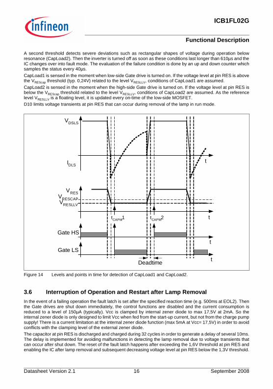
A second threshold detects severe deviations such as rectangular shapes of voltage during operation below resonance (CapLoad2). Then the inverter is turned off as soon as these conditions last longer than 610µs and the IC changes over into fault mode. The evaluation of the failure condition is done by an up and down counter which samples the status every 40µs.CapLoad1 is sensed in the moment when low-side Gate drive is turned on. If the voltage level at pin RES is above the VREScap threshold (typ. 0,24V) related to the level VRESLLV, conditions of CapLoad1 are assumed.CapLoad2 is sensed in the moment when the high-side Gate drive is turned on. If the voltage level at pin RES is below the VREScap threshold related to the level VRESLLV, conditions of CapLoad2 are assumed. As the reference level VRESLLV is a floating level, it is updated every on-time of the low-side MOSFET. D10 limits voltage transients at pin RES that can occur during removal of the lamp in run mode.
Figure 14 Levels and points in time for detection of CapLoad1 and CapLoad2.
3.6 Interruption of Operation and Restart after Lamp RemovalIn the event of a failing operation the fault latch is set after the specified reaction time (e.g. 500ms at EOL2). Then the Gate drives are shut down immediately, the control functions are disabled and the current consumption is reduced to a level of 150µA (typically). Vcc is clamped by internal zener diode to max 17,5V at 2mA. So the internal zener diode is only designed to limit Vcc when fed from the start-up current, but not from the charge pump supply! There is a current limitation at the internal zener diode function (max 5mA at Vcc= 17,5V) in order to avoid conflicts with the clamping level of the external zener diode.The capacitor at pin RES is discharged and charged during 32 cycles in order to generate a delay of several 10ms. The delay is implemented for avoiding malfunctions in detecting the lamp removal due to voltage transients that can occur after shut down. The reset of the fault latch happens after exceeding the 1,6V threshold at pin RES and enabling the IC after lamp removal and subsequent decreasing voltage level at pin RES below the 1,3V threshold.
t
t
t
t
Deadtime
tCAPM1 tCAPM2
VDSLS
IDLS
VRES
VRESLLV
VRESCAP
Gate HS
Gate LS
Datasheet Version 2.1 16 September 2008

ICB1FL02G
Functional Description
The status failure mode is kept as long until a lamp removal is detected (interruption of current across filaments and detection of the return of the current) or the supply voltage drops below UVLO. After a break down of the supply voltage below the undervoltage lockout (UVLO) threshold the IC resets any failure latch and will try to restart as soon as Vcc exceeds the start-up threshold.
An undervoltage (75%) of the bus voltage will not be latched as a fault condition. If the undervoltage lasts longer than 80µs the Gate drives are switched off and the IC tries to restart after a Vcc hysteresis has been passed.
Figure 15 Interruption of operation by a fault condition and subsequent lamp removal.
VCC
14,0V
10,5V
IVCC
VRES
1,6V
IRES
ILVS
<2,5mA
3,2V
IC ACTIVESOFTSTART
t
t
t
t
t< +/- 2,5mA
41µA
20µA 34µA 17µA 20µA
32 CYCLES (>50ms typically)
16,0V
TRANSIENTAT LVS PIN
FAULT LATCHSET E.G. BY EOL
VRES>1,3V
0,375V1,3V
POWERDOWNSIGNAL
tFAULTLATCHSIGNAL t
5mA+ QGate <170µA
5mA+ QGate
ICACTIVE
LAMPREMOVALLS + HSOPEN
>15µA >15µA >15µA
H H
RESET SIGNAL
5,0V
SET SIGNAL
20µA
<3,2V1,6V
1,3V
<150µA
Datasheet Version 2.1 17 September 2008

ICB1FL02G
State Diagram
4 State Diagram
Figure 16 State Diagram
62ms 35ms 10ms 0ms …2000ms 40ms …235ms 250ms 500ms UVLO Monitoring Softstart Preheating Ignition Pre -Run Run
active
active
active
active
active
act,Restart
active
activeactiveactiveactive
activeactiveactive (300ns)activeOvercurrent PFC 1,0V
active (605µs)Capacitive Load 2
activeactiveactiveactive
(80µs)
activeactiveactiveactive>109%
active
active
active
active
active
act,Restart
active
Cap.Load1; EOL1,2
activeactive , & 0,8VactiveactiveOvercurrent Inverter 1,6V
activeactiveactiveactiveOvercurrent PFC 1,0V
activeCapacitive Load 2
activeactiveactiveactiveBUS Open Loop <15%
BUS Undervoltage <75%
activeactiveactiveactiveBUS Overvoltage >109%
Vcc > 14,0V & VRES< 1,6V=> Start 125kHz > f > F_PH;
10,5 < Vcc < 16,0V;f= F_PH
10,5 < Vcc < 16,0V; IRES= 20µA;f= F_RUN
F_PH > f > F_RUN
10,5 < Vcc < 16,0V;f= F_RUN
EarliestStop
by EOL
Fault Mode: disabled by Lamp Removal or UVLO;10,5 < Vcc< 16,0V; IS< 150µA; IRES= 20µA
Mains Switch turned on; 0 < Vcc < 10,5V; IS< 80µA; IRES= 0µA
10,5 < Vcc < 14,0V; IS< 150µA; IRES= 20µA
10,5 < Vcc < 16,0V;
Datasheet Version 2.1 18 September 2008

ICB1FL02G
Protection Functions
5 Protection FunctionsDescription of Fault Fault-Type
Min
. Dur
atio
nof
Effe
ct
Detection active during Consequence
Softs
tart
10m
sPr
ehea
t Mod
e0
- 200
0ms
Igni
tion
Mod
e40
- 23
5ms
Pre-
Run
Mod
e25
0ms
Run
Mod
e
+/- Peak Level of Lamp Voltage above threshold
EOL1 610µs X Power down, latched Fault Mode
Ratio of +/- amplitudes of lamp voltage > 1.15 or < 0.85
EOL2 500ms X Power down, latched Fault Mode
No zero voltage switching Cap.Load 1 500ms X Power down, latched Fault Mode
Voltage at Pin RES > 3.0V Open Filament 500ms X Power down, latched Fault Mode
Bus voltage > 109% of rated levelin active operation
Overvoltage 500ms X Power down, latched Fault Mode
Bus voltage > 109% of rated level10µs after power up
Overvoltage Gate drivers off, restart after VCC hysteresis
Bus voltage > 109% of rated levelin active operation
PFC Overvoltage
5µs X X X X X Turn-off PFC MOSFET until Bus Voltage < 105%
Bus voltage < 75% of rated level Undervoltage 80µs X Gate drivers off, restart after VCC hysteresis
Bus voltage < 15% of rated level Open Loop Detection
1µs X X X X X Power down
Capacitive Load, Operation below resonance
Cap.Load 2 610µs X X Power down, latched Fault Mode
Run frequency can not be achieved No Ignition 235ms X Power down, latched Fault Mode
Voltage at Pin RES > 1.6Vbefore power up
LS open Filament
1ms Prevents power up
Current into Pin LVS1 < 12µA HS open Filament
1ms Prevents power up
Current into Pin LVS2 < 12µA HS open Filament
1ms Prevents power up
Voltage at Pin PFCCS > 1.0V PFC Overcurrent
260ns X X X X X Turn-off PFC MOSFET immediately
Voltage at Pin LSCS > 0.8V Inverter Current Limit
250ns X Increases the Operating Frequency
Voltage at Pin LSCS > 1.6V Inverter Overcurrent
400ns X X X X X Power Down, Latched Fault Mode
Supply voltage at Pin VCC < 14.0Vbefore power up
Below startup threshold
1µs Prevents power up
Supply voltage at Pin VCC < 10.5Vafter power up
Below UVLO threshold
1µs X X X X X Power Down, Reset of Latched Fault Mode
Datasheet Version 2.1 19 September 2008

ICB1FL02G
Electrical Characteristics
6 Electrical CharacteristicsNote: All voltages without the high side signals are measured with respect to ground (pin 4). The high side
voltages are measured with respect to pin17/20. The voltage levels are valid if other ratings are not violated.
6.1 Absolute Maximum RatingsNote: Absolute maximum ratings are defined as ratings, which when being exceeded may lead to destruction
of the integrated circuit. For the same reason make sure, that any capacitor that will be connected to pin 3 (VCC) and pin 18 (HSVCC) is discharged before assembling the application circuit.
Parameter Symbol Limit Values Unit Remarks
min. max.
LSCS Voltage VLSCS -5 6 V
LSCS Current ILSCS -3 3 mA
LSGD Voltage VLSGD -0.3 Vcc+0.3 V internally clamped to 11V
VCC Voltage VVCC -0.3 18 V see VCC Zener Clamp
VCC Zener Clamp Current IVCCzener -5 5 mA IC in Power Down Mode
PFCGD Voltage VPFCGD -0.3 Vcc+0.3 V internally clamped to 11V
PFCCS Voltage VPFCCS -5 6 V
PFCCS Current IPFCCS -3 3 mA
PFCZCD Voltage VPFCZCD -3 6 V
PFCZCD Current IPFCZCD -5 5 mA
PFCVS Voltage VPFCVS -0.3 5.3 V
RFRUN Voltage VRFRUN -0.3 5.3 V
RFPH Voltage VRFPH -0.3 5.3 V
RTPH Voltage VRTPH -0.3 5.3 V
RES Voltage VRES -0.3 5.3 V
LVS1 Current1 ILVS1_1 -1 1 mA IC in Power Down Mode
LVS1 Current2 ILVS1_2 -3 3 mA IC in Active Mode
LVS2 Current1 ILVS2_1 -1 1 mA IC in Power Down Mode
LVS2 Current2 ILVS2_2 -3 3 mA IC in Active Mode
HSGND Voltage VHSGND -900 900 V referring to GND
HSGND, Voltage Transient dVHSGND/dt -40 40 V/ns
HSVCC Voltage VHSVCC -0.3 18 V referring to HSGND
HSGD Voltage VHSGD -0.3 VHSVCC+0.3
V internally clamped to 11Vreferring to HSGND
PFCGD Peak Source Current IPFCGDsomax — 150 mA < 100ns
PFCGD Peak Sink Current IPFCGDsimax — 700 mA < 100ns
LSGD Peak Source Current ILSGDsomax — 75 mA < 100ns
LSGD Peak Sink Current ILSGDsimax — 400 mA < 100ns
HSGD Peak Source Current IHSGDsomax — 75 mA < 100ns
Datasheet Version 2.1 20 September 2008
ICB1FL02G
Electrical Characteristics
6.2 Operating Range
HSGD Peak Sink Current IHSGDsimax — 400 mA < 100ns
Junction Temperature Tj -25 150 °C
Storage Temperature TS -55 150 °C
Max possible Power Dissipation Ptot — 2 W PG-DSO-18-1, Tamb = 25°C
Thermal Resistance (Both Chips) Junction-Ambient
RthJA — 60 K/W PG-DSO-18-1
Thermal Resistance (HS Chips) Junction-Ambient
RthJAHS — 120 K/W PG-DSO-18-1
Thermal Resistance (LS Chips) Junction-Ambient
RthJALS — 120 K/W PG-DSO-18-1
Soldering Temperature 260 °C wave sold. acc.JESD22A111
ESD Capability VESD — 2 kV Human body model1)
1) According to EIA/JESD22-A114-B (discharging an 100pF capacitor through an 1.5kΩ series resistor).
Parameter Symbol Limit Values Unit Remarks
min. max.
HSVCC Supply Voltage VHSVCC VHSVCCoff 17.0 V referring to HSGND
HSGND Supply Voltage VHSGND -900 900 V referring to GND
VCC Supply Voltage VVCC VVCCoff 17.5 V
LSCS Voltage Range VLSCS -4 5 V
PFCVS Voltage Range VPFCVS 0 4 V
PFCCS Voltage Range VPFCCS -4 5 V
PFCZCD Current Range IPFCZCD -4 4 mA
LVS1, LVS2 Voltage Range VLVS1,LVS2 -0.3 1)
1) Limited by maximum of current range at LVS1, LVS2
V IC in Power Down Mode
LVS1, LVS2 Current Range ILVS1,LVS22)
2) Limited by minimum of voltage range at LVS1, LVS2
300 µA IC in Power Down Mode
LVS1, LVS2 Current Range ILVS1,LVS2 -2.5 2.5 mA IC in Active Mode
Junction Temperature Tj -25 125 °C
Adjustable Preheating Frequency Range set by RFPH
FRFPH FRFRUN 150 kHz
Adjustable Run Frequency Range set by RFRUN
FRFRUN 20 100 kHz
Adjustable Preheating Time Range set by RTPH
tRTPH 0 1980 ms
Set Resistor for Run Frequency RFRUN 5 25 kΩ
Set Resistor for Preheating Frequency (RFRUN parallel RFPH)
RFRUNII RFPH
3.3 kΩ
Set Resistor for Preheating Time RTPH 0 20 kΩ
Datasheet Version 2.1 21 September 2008
ICB1FL02G
Electrical Characteristics
6.3 Characteristics
6.3.1 Power Supply SectionNote: The electrical characteristics involve the spread of values given within the specified supply voltage and
junction temperature range TJ from – 25 °C to 125 °C. Typical values represent the median values, which are related to 25°C. If not otherwise stated, a supply voltage of VCC = 15 V and VHSVCC = 15V is assumed and the IC operates in active mode. Furthermore all voltages are referring to GND if not otherwise mentioned.
Parameter Symbol Limit Values Unit Test Condition
min. typ. max.
High Side Leakage Current IHSGNDleak 0.01 2 µA VHSGND = 800VVGND = 0V
VCC Quiescent Current IVCCqu1 80 120 µA VVCC = VVCCoff - 0.5V
VCC Quiescent Current IVCCqu2 110 150 µA VVCC = VVCCon - 0.5V
VCC Supply Current with Inactive Gates
IVCCsup1 5 7 mA VPFCVS > 2.725V
VCC Supply Current in Latched Fault Mode
IVCClatch — 110 170 µA VRES = 5V
LS VCC Turn-On ThresholdLS VCC Turn-Off ThresholdLSVCC Turn-On/Off Hysteresis
VVCConVVCCoffVVCChys
13.610.03.2
14.110.53.6
14.611.04.0
VVV
VCC Zener Clamp Voltage VVCCclmp 15.7 16.3 16.9 V IVCC = 2mAVRES = 5V
VCC Zener Clamp Current IVCCzener 2.5 — 5 mA VVCC = 17.5VVRES = 5V
HSVCC Quiescent Current IHSVCCqu1)
1) With reference to High Side Ground HSGND
— 170 250 µA VHSVCC = VHSVCCon -0.5V
HSVCC Supply Current with Inactive Gate
IHSVCCsup11) — 0.65 1.2 mA
HSVCC Turn-On ThresholdHSVCC Turn-Off ThresholdHSVCC Turn-On/Off Hysteresis
VHSVCCon1)
VHSVCCoff1)
VHSVCChys1)
9.67.91.4
10.18.41.7
10.79.12.0
VVV
Datasheet Version 2.1 22 September 2008

ICB1FL02G
Electrical Characteristics
6.3.2 PFC Section
6.3.2.1 PFC Current Sense (PFCCS)
6.3.2.2 PFC Zero Current Detector (PFCZCD)
6.3.2.3 PFC Bus Voltage Sense (PFCVS)
Parameter Symbol Limit Values Unit Test Condition
min. typ. max.
Turn-Off Threshold VPFCCSoff 0.95 1.0 1.05 V
Duration of Overcurrent for turn-off tPFCCSoff 200 250 320 ns
Spike Blanking tblanking 140 200 260 ns
PFCCS Bias Current IPFCCSbias -0.5 0.5 µA VPFCCS = 1.5V
Parameter Symbol Limit Values Unit Test Condition
min. typ. max.
Zero Crossing Upper Threshold VPFCZCDup 1.4 1.5 1.6 V
Zero Crossing Lower Threshold VPFCZCDlow 0.4 0.5 0.6 V
Zero Crossing Hysteresis VPFCZCDhys 1.0 V
Clamping of Positive Voltages VPFCZCDpclp 5.0 6.3 7.2 V IPFCZCD = 4mA
Clamping of Negative Voltages VPFCZCDnclp -3.5 -2.9 -2.0 V IPFCZCD = 4mA
PFCZCD Bias Current IPFCZCDbias -0.5 0.5 µA VPFCZCD = 1.7V
PFCZCD Ringing Suppression Time tringsup 350 500 650 ns
Parameter Symbol Limit Values Unit Test Condition
min. typ. max.
Trimmed Reference Voltage VPFCVSref 2.47 2.5 2.53 V
Overvoltage Upper Detection Limit VPFCVSup 2.675 2.725 2.78 V
Overvoltage Lower Detection Limit VPFCVSlow 2.57 2.625 2.67 V
Overvoltage Hysteresis VPFCVShys 70 100 130 mV
Undervoltage Detection Limit VPFCVSuv 1.79 1.83 1.87 V
Undervoltage Shut Down VPFCVSsd 0.30 0.375 0.45 V
Bias Current (ESD-Stress<1KV) IPFCVSbias -1 1 µA VPFCVS = 2.5V
Bias Current (ESD-Stress>1KV) IPFCVSbias -2.5 2.5 µA VPFCVS = 2.5V
Datasheet Version 2.1 23 September 2008

ICB1FL02G
Electrical Characteristics
6.3.2.4 PFC PWM Generation
6.3.2.5 PFC Gate Drive (PFCGD)
Parameter Symbol Limit Values Unit Test Condition
min. typ. max.
Initial On-Time tPFCon-initial 2.0 3.0 3.8 µs VPFCZCD = 0V
Max. On-Time tPFCon-max 19 23.5 28 µs 0.45V < VPFCVS < 2.45V
Repetition Time when missing Zero Crossing
tPFCrep 38 50 62 µs VPFCZCD = 0V
Off-time when missing ZCD Signal tPFCoff 35 42 49 µs VPFCZCD = 0V
Parameter Symbol Limit Values Unit Test Condition
min. typ. max.
PFCGD Low Voltage VPFCGDlow 0.4 0.7 0.9 V IPFCGD = 5mA
0.4 0.75 1.1 V IPFCGD = 20mA
-0.1 0.3 0.6 V IPFCGD = -20mA
PFCGD High Voltage VPFCGDhigh 10.2 11 11.8 V IPFCGD = -20mA
9.0 — — V IPFCGD = -1mAVVCC = VVCCoff + 0.3V
8.5 — — V IPFCGD = -5mAVVCC = VVCCoff + 0.3V
PFCGD Voltage Active Shut Down VPFCGDsd 0.4 0.75 1.1 V IPFCGD = 20mAVVCC = 5V
PFCGD Peak Source Current IPFCGDsource — 100 — mA Rload = 4Ω + CLoad = 3.3nF1)
1) The parameter is not subject to production test - verified by design/characterization
PFCGD Peak Sink Current IPFCGDsink — -500 — mA Rload = 4Ω + CLoad = 3.3nF1)
PFCGD Rise Time2V < VLSGD < 8V
tPFCGDrise 110 220 400 ns Rload = 4Ω + CLoad = 3.3nF
PFCGD Fall Time8V > VLSGD > 2V
tPFCGDfall 20 45 70 ns Rload = 4Ω + CLoad = 3.3nF
Datasheet Version 2.1 24 September 2008

ICB1FL02G
Electrical Characteristics
6.3.3 Inverter Section
6.3.3.1 Inverter Control (RFRUN, RFPH, RTPH)
6.3.3.2 Inverter Low Side Current Sense (LSCS)
Parameter Symbol Limit Values Unit Test Condition
min. typ. max.
Fixed Start-Up Frequency Fstartup 112 125 138 kHz
Duration of Soft Start, shift F from Start-Up to Preheating Frequency
tsoftstart 9.0 11.0 13.5 ms
Preheating Frequency FRFPH1 97.0 100 103.0 kHz RRFPH = 10kΩRRFRUN = 10kΩ
Run Frequency FRFRUN1 49.0 50.0 51.0 kHz RRFRUN = 10kΩ
Preheating Time tRTPH1 720 900 1080 ms RRTPH = 8.06kΩ
Preheating Time tRTPH2 50 90 130 ms RRTPH = 806Ω1)
Current Source Preheating Time IRTPH 132 140 148 µA
Min. Duration of Ignition, shift F from Preheating to Run Frequency
tIGNITION 34 40 48 ms 1)
1) The parameter is not subject to production test - verified by design/characterization
Max. Duration of Ignition, shift F from Preheating to Run Frequency
tNOIGNITION 210 235 290 ms 1)
Duration of Pre-Run, time period after operating frequency has reached Run Frequency first time after ignition
tPRERUN 210 250 290 ms 1)
Minimum Duration of fault condition by EOL2, Cap.Load 1, Open filament and Overvoltage for entering latched Fault Mode
tCAPLOAD1 420 500 580 ms 1)
Minimum Duration of fault condition by EOL1, Cap.Load 2 for entering latched Fault Mode
tCAPLOAD2 520 610 770 µs
Parameter Symbol Limit Values Unit Test Condition
min. typ. max.
Current Limit Threshold during Ignition Mode
VLSCSlimit 0.76 0.80 0.84 V
Duration of Current above Threshold for enabling Frequency Increase
tLSCSlimit 200 250 320 ns
Overcurrent Shut Down Threshold VLSCSovc 1.55 1.60 1.65 V
Duration of Overcurrent for entering Latched Fault Mode
tLSCSovc 320 400 480 ns
Bias Current LSCS ILSCSbias -0.5 0.5 µA VLSCS = 1.5V
Inverter Dead Time between LS off and HS on
tdeadtime 1.50 1.75 2.0 µs
Datasheet Version 2.1 25 September 2008
ICB1FL02G
Electrical Characteristics
6.3.3.3 Restart after Lamp Removal (RES)
6.3.3.4 Lamp Voltage Sense (LVS1, LVS2)
Parameter Symbol Limit Values Unit Test Condition
min. typ. max.
Low-side Open Filament Threshold VRESofil 3.1 3.2 3.3 V
Capacitive Load Detection Threshold VREScap 0.18 0.24 0.30 V
Discharge Resistor during Latched Fault Mode
RRESdisch 37 56 75 kΩ
I1 Current Source IRES1 -54.3 -41 -30.0 µA VRES=1V; LVS1=5µA
I2 Current Source IRES2 -46 -34 -24.2 µA VRES=2V; LVS1=5µA
I3 Current Source IRES3 -27.0 -20 -15.1 µA VRES=1V; LVS1=50µA
I4 Current Source IRES4 -22.6 -17 -12.3 µA VRES=2V; LVS1=50µA
C1 Comparator Threshold VRESC1 1.55 1.6 1.65 V
C2 Comparator Threshold VRESC2 1.25 1.3 1.35 V
C3 Comparator Threshold VRESC3 0.32 0.375 0.46 V
Parameter Symbol Limit Values Unit Test Condition
min. typ. max.
Source Current before Start Up ILVSsource -8 -5 -2 µA 11 < VVCC < 13VVLVS = 0V
Threshold for enabling Lamp Monitoring
VLVSenable 1.5 2.3 3.0 V 11 < VVCC < 13V
Sink Current Threshold for Lamp Detection
ILVSsink 9 15 26 µA VLVS > VVCC
Positive EOL Current Threshold ILVSpEOLAC 185 215 250 µA T > 0°C, AC input
Negative EOL Current Threshold ILVSnEOLAC -250 -215 -185 µA T > 0°C, AC input
EOL Current Threshold ILVSEOLDC +/-145 +/-175 +/-210 µA T > 0°C, DC input
Maximum Ratio between positive and negative Current Amplitude1)
ROLVS1MAXROLVS2MAX
1.1 1.2 1.3 ILVSsourpeak=150µAILVSsinkpeak= increasing
Minimum Ratio between positive and negative Current Amplitude1)
ROLVS1MINROLVS2MIN
0.75 0.85 0.95 ILVSsinkpeak=150µAILVSsourcepeak= increasing
Positive Clamping Voltage ILVSclmp - VVCC + 1V
- V ILVS = 300µA
Datasheet Version 2.1 26 September 2008
ICB1FL02G
Electrical Characteristics
6.3.3.5 Inverter Low Side Gate Drive (LSGD)
1) Referring to the following equations:
Parameter Symbol Limit Values Unit Test Condition
min. typ. max.
LSGD Low Voltage VLSGDlow 0.4 0.7 1.0 V ILSGD = 5mA
0.5 0.8 1.2 V ILSGD = 20mA
-0.3 0.1 0.4 V ILSGD = -20mA
LSGD High Voltage VLSGDhigh 10.0 10.8 11.6 V IPFCGD = -20mA
9.0 — — V IPFCGD = -1mAVVCC = VVCCoff + 0.3V
8.5 — — V IPFCGD = -5mAVVCC = VVCCoff + 0.3V
LSGD Voltage Active Shut Down VLSGDsd 0.5 0.8 1.2 V IHSGD = 20mAVHSVCC = 5V
LSGD Peak Source Current ILSGDsource — 50 — mA Rload = 10Ω + CLoad = 1nF1)
1) The parameter is not subject to production test - verified by design/characterization
LSGD Peak Sink Current ILSGDsink — -300 — mA Rload = 10Ω + CLoad = 1nF1)
LSGD Rise Time2V < VLSGD < 8V
tLSGDrise 110 220 400 ns Rload = 10Ω + CLoad = 1nF
LSGD Fall Time8V > VLSGD > 2V
tLSGDfall 20 35 60 ns Rload = 10Ω + CLoad = 1nF
ROLVSILVS kpeaksin n 1+( )
ILVSsourcepeak n( )--------------------------------------------------------= ROLVS
ILVSsource n 2+( )
ILVS kpsin eak n 1+( )--------------------------------------------------------=
Datasheet Version 2.1 27 September 2008
ICB1FL02G
Electrical Characteristics
6.3.3.6 Inverter High Side Gate Drive (HSGD)
Parameter Symbol Limit Values Unit Test Condition
min. typ. max.
HSGD Low Voltage VHSGDlow 0.02 0.05 0.1 V IHSGD = 5mA
0.5 1.1 2.5 V IHSGD = 100mA
-0.4 -0.2 -0.05 V IHSGD = -20mA
HSGD High Voltage VHSGDhigh 9.5 10.5 11.0 V IHSGD = -20mA
7.8 — — V IHSGD = -1mAVHSVCC = VHSVCCoff + 0.3V
HSGD Voltage Active Shut Down VHSGDsd 0.05 0.22 0.50 V IHSGD = 20mAVHSVCC = 5V
HSGD Peak Source Current IHSGDsource — 50 — mA Rload = 10Ω + CLoad = 1nF1)
1) The parameter is not subject to production test - verified by design/characterization
HSGD Peak Sink Current IHSGDsink — -300 — mA Rload = 10Ω + CLoad = 1nF1)
HSGD Rise Time2V < VHSGD < 8V
tHSGDrise 140 220 300 ns Rload = 10Ω + CLoad = 1nF
HSGD Fall Time8V > VHSGD > 2V
tHSGDfall 20 35 70 ns Rload = 10Ω + CLoad = 1nF
Datasheet Version 2.1 28 September 2008
ICB1FL02G
Application Examples
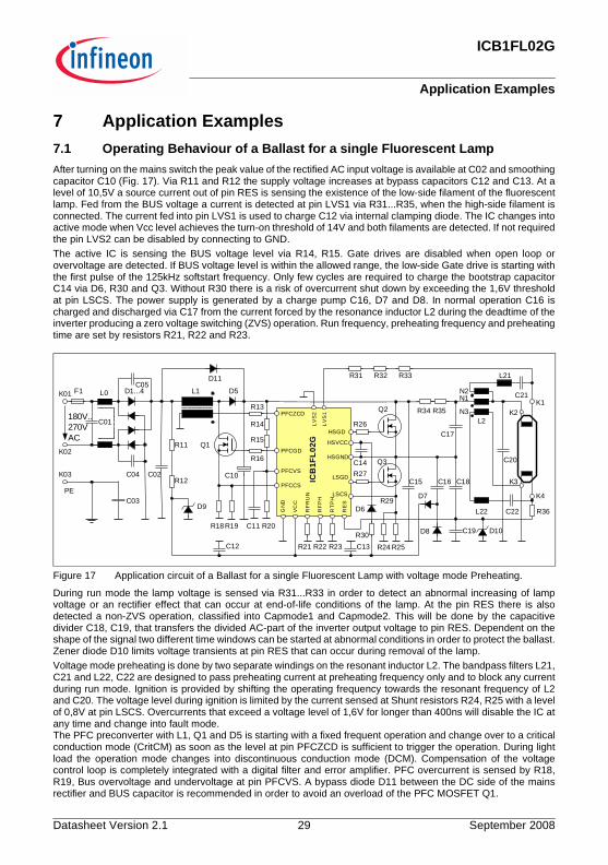
7 Application Examples7.1 Operating Behaviour of a Ballast for a single Fluorescent LampAfter turning on the mains switch the peak value of the rectified AC input voltage is available at C02 and smoothing capacitor C10 (Fig. 17). Via R11 and R12 the supply voltage increases at bypass capacitors C12 and C13. At a level of 10,5V a source current out of pin RES is sensing the existence of the low-side filament of the fluorescent lamp. Fed from the BUS voltage a current is detected at pin LVS1 via R31...R35, when the high-side filament is connected. The current fed into pin LVS1 is used to charge C12 via internal clamping diode. The IC changes into active mode when Vcc level achieves the turn-on threshold of 14V and both filaments are detected. If not required the pin LVS2 can be disabled by connecting to GND.The active IC is sensing the BUS voltage level via R14, R15. Gate drives are disabled when open loop or overvoltage are detected. If BUS voltage level is within the allowed range, the low-side Gate drive is starting with the first pulse of the 125kHz softstart frequency. Only few cycles are required to charge the bootstrap capacitor C14 via D6, R30 and Q3. Without R30 there is a risk of overcurrent shut down by exceeding the 1,6V threshold at pin LSCS. The power supply is generated by a charge pump C16, D7 and D8. In normal operation C16 is charged and discharged via C17 from the current forced by the resonance inductor L2 during the deadtime of the inverter producing a zero voltage switching (ZVS) operation. Run frequency, preheating frequency and preheating time are set by resistors R21, R22 and R23.
Figure 17 Application circuit of a Ballast for a single Fluorescent Lamp with voltage mode Preheating.
During run mode the lamp voltage is sensed via R31...R33 in order to detect an abnormal increasing of lamp voltage or an rectifier effect that can occur at end-of-life conditions of the lamp. At the pin RES there is also detected a non-ZVS operation, classified into Capmode1 and Capmode2. This will be done by the capacitive divider C18, C19, that transfers the divided AC-part of the inverter output voltage to pin RES. Dependent on the shape of the signal two different time windows can be started at abnormal conditions in order to protect the ballast. Zener diode D10 limits voltage transients at pin RES that can occur during removal of the lamp.Voltage mode preheating is done by two separate windings on the resonant inductor L2. The bandpass filters L21, C21 and L22, C22 are designed to pass preheating current at preheating frequency only and to block any current during run mode. Ignition is provided by shifting the operating frequency towards the resonant frequency of L2 and C20. The voltage level during ignition is limited by the current sensed at Shunt resistors R24, R25 with a level of 0,8V at pin LSCS. Overcurrents that exceed a voltage level of 1,6V for longer than 400ns will disable the IC at any time and change into fault mode. The PFC preconverter with L1, Q1 and D5 is starting with a fixed frequent operation and change over to a critical conduction mode (CritCM) as soon as the level at pin PFCZCD is sufficient to trigger the operation. During light load the operation mode changes into discontinuous conduction mode (DCM). Compensation of the voltage control loop is completely integrated with a digital filter and error amplifier. PFC overcurrent is sensed by R18, R19, Bus overvoltage and undervoltage at pin PFCVS. A bypass diode D11 between the DC side of the mains rectifier and BUS capacitor is recommended in order to avoid an overload of the PFC MOSFET Q1.
RFR
UN
RFP
H
RTP
H
VC
C
PFCZCD
PFCGD
PFCVS
PFCCS
HSGD
HSVCC
HSGND
LSGD
LSCS
LVS
2
RE
S
GN
D
180V..270VAC
ICB
1FL0
2GR11
R12
D1...4L0 L1 D5
Q1R15
R14
R13
R16
R18
D9
C01
C10
C11R19
R21 R22 R23
R26
R27C14
C13
Q2
Q3
R24
R35R34
R31 R32 R33
R36
C17
C16 C18
C19
C20
L2
D6
D7
D8
R29
C12
LVS
1
C21
C22
L21
L22
F1
C02
C05
C04
C03PE
C15
R20
R25
N1N2
N3K1
K2
K3
K4
R30
K01
K02
K03
D10
D11
Datasheet Version 2.1 29 September 2008

ICB1FL02G
Application Examples
7.2 Design Equations of a Ballast ApplicationSubsequent the design equations are listed:
Start-up resistors R11, R12:
Selected value: R11= 470k; R12= 470k
Current limitation resistor R13 of PFC zero current detector (PFCZCD). The additional factor 2 is used in order to keep away from limit value.
Selected value: R13= 33k.
PFC Voltage sense resistor R20:
Selected value: R20= 10k.
PFC Voltage sense resistors R14, R15:
Selected values: R14= 820k; R15= 820k
Low pass capacitor C11:Selected corner frequency fC1= 10kHz.
Selected value C3= 2,2nF
PFC Shunt resistors R18, R19:
Selected values: R18= 2,2Ohm; R19= 2,2Ohm
R11 R12+VINMINIVCCqu2------------------------- 200V
150µA----------------- 1 33MΩ,= = =
R13VBUS NSEC 2⋅ ⋅
IPFCZCD NPRIM 1⋅ ⋅----------------------------------------------------------- 410V 13 2⋅ ⋅
4mA 128 1⋅ ⋅--------------------------------- 20 8kΩ,= = =
R20VREF
100 IPFCBIAS⋅------------------------------------------≤ 2 50V,
100 2 5µA,⋅------------------------------- 10kΩ= =
R14 R15+VBUS VREF–
VREF--------------------------------------- R20⋅ 410V 2 5V,( )–
2 5V,-------------------------------------- 10k⋅ 1630kΩ= = =
C111 R20 R14 R15+ +( )⋅
2 π fC1 R20 R14 R15+( )⋅ ⋅ ⋅ ⋅--------------------------------------------------------------------------- 1 10k 820k 820k+ +( )⋅
2 π 10kHz 10k 820k 820k+( )⋅ ⋅ ⋅ ⋅--------------------------------------------------------------------------------------- 1 60nF,= = =
R18 R19⋅
R18 R19+--------------------------
VPFCCSOFF η VINACMIN 2⋅ ⋅ ⋅
4 POUTPFC⋅---------------------------------------------------------------------------------------------- 1V 0 95, 180V 2⋅ ⋅ ⋅
4 55W⋅------------------------------------------------------ 1 1Ω,= = =
Datasheet Version 2.1 30 September 2008

ICB1FL02G
Application Examples
Set resistor R21 for run frequency, at a projected run frequency of 45kHz:
Selected value: R21= 11,0k
Set resistor R22 for preheating frequency, at a projected preheating frequency of 105kHz:
Selected value: R22= 8,2k
Set resistor R23 for preheating time, at a projected preheating time of 900ms:
Selected value: R23= 8,2k
Gate drive resistors R16, R26, R27 are recommended to be equal or higher than 10Ohm.
Shunt resistors R24, R25:The selected lamp type 54W-T5 requires an ignition voltage of VIGN= 800V peak. In our application example the resonant inductor is evaluated to L2= 1,46mH and the resonant capacitor C20= 4,7nF. With this inputs we can calculate the ignition frequency fIGN :
The second solution of this equation (with the minus sign) leads to a result of 50163Hz, which is on the capacitive side of the resonant rise. This value is no solution, because the operating frequency approaches from the higher frequency level.In the next step we can calculate the current through the resonant capacitor C20 when reaching a voltage level of 800V peak.
Finally the resistors R24, R25 can be calculated from IC20 and the current limitation threshold during ignition mode.
Selected values are R24= 0,82Ohm; R25= 0,82Ohm.
R21 RFRUN5 108
ΩHz⋅ ⋅fRUN
--------------------------------- 5 108ΩHz⋅ ⋅
45kHz--------------------------------- 11 1kΩ,= = = =
R22 RFPHRFRUN
fPH RFRUN⋅
5 108ΩHz⋅ ⋅
------------------------------------ 1–
--------------------------------------------- 11 0k,105kHz 11 0k,⋅
5 108ΩHz⋅ ⋅
---------------------------------------- 1–------------------------------------------------- 8 4kΩ,= = = =
R23 RTPHTPH ms[ ]
112ms( ) kΩ( )⁄-------------------------------------- 900ms
112ms( ) kΩ( )⁄-------------------------------------- 8 93kΩ,= = = =
fIGN
1VBUS 2⋅
π VIGN⋅------------------------±
4 π2 L2 C20⋅ ⋅ ⋅
----------------------------------------1 410V 2⋅
π 800V⋅---------------------±
4 π2 1 46mH, 4 7nF,⋅ ⋅ ⋅
------------------------------------------------------------- 69759Hz= = =
IC20 VIGN 2 π fIGN C20⋅ ⋅ ⋅ ⋅ 800V 2 π 69759Hz 4 7nF,⋅ ⋅ ⋅ ⋅ 1 65A,= = =
R24 R25⋅
R24 R25+--------------------------
VLSCSLIMITIC20
--------------------------------------- 0 8V,1 65A,---------------- 0 485Ω,= = =
Datasheet Version 2.1 31 September 2008

ICB1FL02G
Application Examples
Lamp voltage sense resistors R31, R32, R33:The selected lamp type 54W-T5 has a typical run voltage of 167V peak. We decide to set the EOL-thresholds at a level of 1,5 times the run voltage level (= 250,5V peak).
Selected values: R31= 390k; R32= 390k; R33= 390k (=1170k).
Current source resistors R34, R35 for detection of high-side filament:
Selected values: R34= 2,2M; R35= 2,2M;
Current limitation resistor R30 for floating bootstrap capacitor C14:A factor of 2 is provided in order to keep current level significant below LSCS turn-off threshold.
Selected value: R30= 10Ohm.
Low-side filament sense resistor R36:For a single lamp ballast
Selected value: R36= 56k
Selected values in a topology with 2 lamps in parallel: R36A= 110k; R36B= 110k.
Low pass filter capacitor C19:Capacitor C19 provides a low pass filter together with resistor R36 in order to suppress AC voltage drop at the low-side filament. When we estimate an AC voltage of 10V peak-to-peak at low-side filament during run mode at fRUN= 40kHz, we need a suppression of at least a factor FLP= 100 (-40dB).
Selected value for better ripple suppression: C19= 22nF.
R31 R32 R33+ +VLEOL
ILVSEOL--------------------------- 250 5V,
215µA------------------- 1165kΩ= = =
R34 R35+VINMIN
ILVSSINKMAX--------------------------------------------- R31 R32 R33+ +( )– 200V
26µA-------------- 1170k( )– 6522kΩ= = =
R302 VCCON⋅
VLSCSOVC----------------------------------
R24 R25⋅
R24 R25+--------------------------⋅≥ 2 14V⋅
1 6V,------------------ 0 82, 0 82,⋅
0 82, 0 82,+------------------------------⋅ 7 18Ω,= =
R36VRESC1MIN
IRES3MIN-------------------------------------≤ 1 55V,
27 0µA,-------------------- 57 4kΩ,= =
R36AVRESC1MAX
IRES3MAX---------------------------------------≥ 1 65V,
15 1µA,-------------------- 109 3kΩ,= =
C19FLP
2 1–
2 π fRUN R36⋅ ⋅ ⋅( )-------------------------------------------------- 1002 1–
2 π 40kHz 56k⋅ ⋅ ⋅( )--------------------------------------------------- 7 1nF,= = =
Datasheet Version 2.1 32 September 2008

ICB1FL02G
Application Examples
Detection of capacitive mode operation via C18:The DC level at pin RES is set by R36 and the source current IRES3. The preferred AC level is in the range between ∆VACRES= 1,5V to 2,0V at a ∆VBUS= 410V.
Selected value: C18= 82pF.
Bandpass filters L21/C21 and L22/C22 can be used in order to conduct filament currents preferred at preheating frequency and to suppress these currents during run mode.
Inductor L1 of the boost converter:The inductivity of the boost inductor typically is designed to operate within a specified voltage range above a minimum frequency in order to get an easier RFI suppression. It is well known, that in critical conduction mode (CritCM) there is a minimum operating frequency at low input voltages and another minimum at maximum input voltage. In state-of-the-art CritCM PFC controllers we use the lowest value out of these two criterias:At minimum AC input voltage:
At maximum AC input voltage
With the new control principle for the PFC preconverter we have a third criteria that covers the maximum on-time tPFCOM-MAX= 23,5µs:
With the assumed conditions the lowest value out of LA, LB, LC is 1,58mH.Selected value: L1= 1,58mH.
C18 C19∆VACRES
∆VBUS-----------------------------⋅ 22nF 2V
410V-------------⋅ 107pF= = =
LAVINACMIN 2⋅( )
2VBUS VINACMIN 2⋅( )–( ) η⋅ ⋅
4 FMIN POUTPFC VBUS⋅ ⋅ ⋅------------------------------------------------------------------------------------------------------------------------------------------------=
LA180V 2⋅( )
2410V 180V 2⋅( )–( ) 0 95,⋅ ⋅
4 25kHz 60W 410V⋅ ⋅ ⋅------------------------------------------------------------------------------------------------------------- 3 89mH,= =
LBVINACMAX 2⋅( )
2VBUS VINACMAX 2⋅( )–( ) η⋅ ⋅
4 FMIN POUTPFC VBUS⋅ ⋅ ⋅-----------------------------------------------------------------------------------------------------------------------------------------------------=
LB270V 2⋅( )
2410V 270V 2⋅( )–( ) 0 95,⋅ ⋅
4 25kHz 60W 410V⋅ ⋅ ⋅------------------------------------------------------------------------------------------------------------- 1 58mH,= =
LCVINACMIN 2⋅( )
2TONMAX η⋅ ⋅
4 POUTPFC⋅----------------------------------------------------------------------------------------------=
LC180 2⋅( )
223 5µs, 0 95,⋅ ⋅
4 60W⋅-------------------------------------------------------------------- 6 03mH,= =
Datasheet Version 2.1 33 September 2008
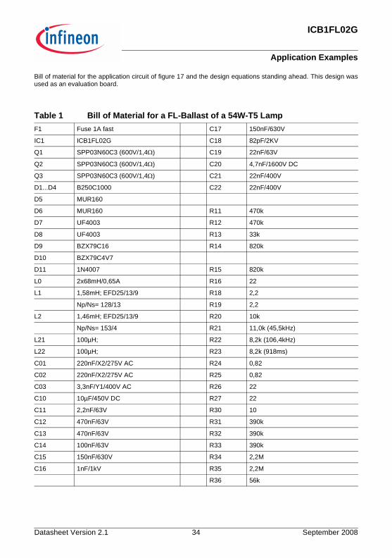
ICB1FL02G
Application Examples
Bill of material for the application circuit of figure 17 and the design equations standing ahead. This design was used as an evaluation board.
Table 1 Bill of Material for a FL-Ballast of a 54W-T5 LampF1 Fuse 1A fast C17 150nF/630V
IC1 ICB1FL02G C18 82pF/2KV
Q1 SPP03N60C3 (600V/1,4Ω) C19 22nF/63V
Q2 SPP03N60C3 (600V/1,4Ω) C20 4,7nF/1600V DC
Q3 SPP03N60C3 (600V/1,4Ω) C21 22nF/400V
D1...D4 B250C1000 C22 22nF/400V
D5 MUR160
D6 MUR160 R11 470k
D7 UF4003 R12 470k
D8 UF4003 R13 33k
D9 BZX79C16 R14 820k
D10 BZX79C4V7
D11 1N4007 R15 820k
L0 2x68mH/0,65A R16 22
L1 1,58mH; EFD25/13/9 R18 2,2
Np/Ns= 128/13 R19 2,2
L2 1,46mH; EFD25/13/9 R20 10k
Np/Ns= 153/4 R21 11,0k (45,5kHz)
L21 100µH; R22 8,2k (106,4kHz)
L22 100µH; R23 8,2k (918ms)
C01 220nF/X2/275V AC R24 0,82
C02 220nF/X2/275V AC R25 0,82
C03 3,3nF/Y1/400V AC R26 22
C10 10µF/450V DC R27 22
C11 2,2nF/63V R30 10
C12 470nF/63V R31 390k
C13 470nF/63V R32 390k
C14 100nF/63V R33 390k
C15 150nF/630V R34 2,2M
C16 1nF/1kV R35 2,2M
R36 56k
Datasheet Version 2.1 34 September 2008

ICB1FL02G
Application Examples
7.3 Multilamp Ballast TopologiesHow to use ICB1FL02G in multi-lamp topologies is demonstrated in the subsequent figures. In figure 18 we see an application for a single lamp with current mode preheating. Compared with figure 17 the difference is the connection of the resonant capacitor in series with the filaments. In respect of operating behaviour the current mode preheating cannot be designed with same variation of operating parameters: the preheating current is typically lower and lamp voltage during preheating higher than in topologies with voltage mode preheating.
Figure 18 Application Circuit of a Ballast for a single Fluorescent Lamp with current mode Preheating.
A topology for two lamps is shown in figure 19. Both lamps including their individual resonant circuit are operating in parallel at the same inverter output. Such a topology can be done with voltage mode preheating in the same way. As the control IC is designed to operate such a 2-lamp topology without restrictions in respect to the monitoring functions, the IC-specific effort is to activate the second lamp voltage sense (LVS2) and an additional resistor at pin RES in order to sense the lamp removal of the second low-side filament.
Figure 19 Application circuit of a Ballast for two Fluorescent Lamps in parallel with current mode Preheating.
Beside a topology with paralleled lamps it is possible of course to use two lamps in series. In this way we come to a 4-lamp topology shown in figure 20. The lamp voltage is sensed of each of the two series connections. The lamp removal is detected on the high-side filaments of the high-side lamps and on the low-side filaments of the
RF
RU
N
RF
PH
RT
PH
VC
C
PFCZCD
PFCGD
PFCVS
PFCCS
HSGD
HSVCC
HSGND
LSGD
LSCS
LVS
2
LVS
1
GN
D
90 ...270 VAC
ICB
1FL0
2G
RE
S
RF
RU
N
RF
PH
RT
PH
VC
C
PFCZCD
PFCGD
PFCVS
PFCCS
HSGD
HSVCC
HSGND
LSGD
LSCS
LVS
2
LVS
1
GN
D
90 ...270 VAC
ICB
1FL0
2G
RE
S
Datasheet Version 2.1 35 September 2008

ICB1FL02G
Package Outlines
low-side lamps. In this way ICB1LB02G supports multi-lamp topologies with all required monitoring functions with a low number of external components.
Figure 20 Application circuit of a Ballast for four Fluorescent Lamps with voltage mode Preheating.
8 Package Outlines
Figure 21 Package dimensions and mechanical data (Dimensions in mm).
RFR
UN
RFP
H
RTP
H
VC
C
PFCZCD
PFCGD
PFCVS
PFCCS
HSGD
HSVCC
HSGND
LSGD
LSCS
LVS
2
LVS
1
GN
D
90 ...270 VAC
ICB
1FL0
2G
RE
S
-0.2
Index Marking
1 10
+0.150.35
0.2
0.2
20
2)
11
20x
2.45
2.65
MA
X.
0.110.3
-0.1 -0
.2
7.6
±0.3
1)
Does not include plastic or metal protrusions of 0.15 max per side2)1)
Does not include dambar protrusion of 0.05 max per side
1.27
0.23
+ 0.0
9
MAX
.8°
0.35 x 45°
+0.80.4
12.8 -0.21)
PG-DSO-18-2(Plastic Dual Small Outline)
Datasheet Version 2.1 36 September 2008

Qualität hat für uns eine umfassende Bedeutung. Wir wollen allen Ihren Ansprüchen in der bestmöglichen Weise gerecht werden. Es geht uns also nicht nur um die Produktqualität – unsere Anstrengungen gelten gleichermaßen der Lieferqualität und Logistik, dem Service und Support sowie allen sonstigen Beratungs- und Betreuungsleistungen.Dazu gehört eine bestimmte Geisteshaltung unserer Mitarbeiter. Total Quality im Denken und Handeln gegenüber Kollegen, Lieferanten und Ihnen, unserem Kunden. Unsere Leitlinie ist jede Aufgabe mit „Null Fehlern“ zu lösen – in offener Sichtweise auch über den eigenen Arbeitsplatz hinaus – und uns ständig zu verbessern.Unternehmensweit orientieren wir uns dabei auch an „top“ (Time Optimized Processes), um Ihnen durch größere Schnelligkeit den entscheidenden Wettbewerbsvorsprung zu verschaffen.Geben Sie uns die Chance, hohe Leistung durch umfassende Qualität zu beweisen.Wir werden Sie überzeugen.
Quality takes on an all encompassing significance at Semiconductor Group. For us it means living up to each and every one of your demands in the best possible way. So we are not only concerned with product quality. We direct our efforts equally at quality of supply and logistics, service and support, as well as all the other ways in which we advise and attend to you.Part of this is the very special attitude of our staff. Total Quality in thought and deed, towards co-workers, suppliers and you, our customer. Our guideline is “do everything with zero defects”, in an open manner that is demonstrated beyond your immediate workplace, and to constantly improve.Throughout the corporation we also think in terms of Time Optimized Processes (top), greater speed on our part to give you that decisive competitive edge.Give us the chance to prove the best of performance through the best of quality – you will be convinced.
h t t p : / / w w w . i n f i n e o n . c o m
Total Quality Management
Published by Infineon Technologies AG