ICAL ENG - vvitengineeringvvitengineering.com/lab/EC6612-VLSI DESIGN-LABORATORY.pdf · ec6612- vlsi...
74
EC6612 VLSI DESIGN LAB 1 VVIT DEPARTMENT OF ELECTRONICS AND COMMUNICATION ENGINEERING Dharmapuri – 636 703 Regulation : 2013 Branch : B.E. – ECE Year & Semester : III Year / VI Semester ICAL ENG EC6612- VLSI DESIGN LABORATORY LAB MANUAL
Transcript of ICAL ENG - vvitengineeringvvitengineering.com/lab/EC6612-VLSI DESIGN-LABORATORY.pdf · ec6612- vlsi...
EC6612 VLSI DESIGN LAB 1
VVIT DEPARTMENT OF ELECTRONICS AND COMMUNICATION ENGINEERING
Dharmapuri – 636 703
Regulation : 2013
Branch : B.E. – ECE
Year & Semester : III Year / VI Semester
ICAL ENG
EC6612- VLSI DESIGN LABORATORY
LAB MANUAL
EC6612 VLSI DESIGN LAB 2
VVIT DEPARTMENT OF ELECTRONICS AND COMMUNICATION ENGINEERING
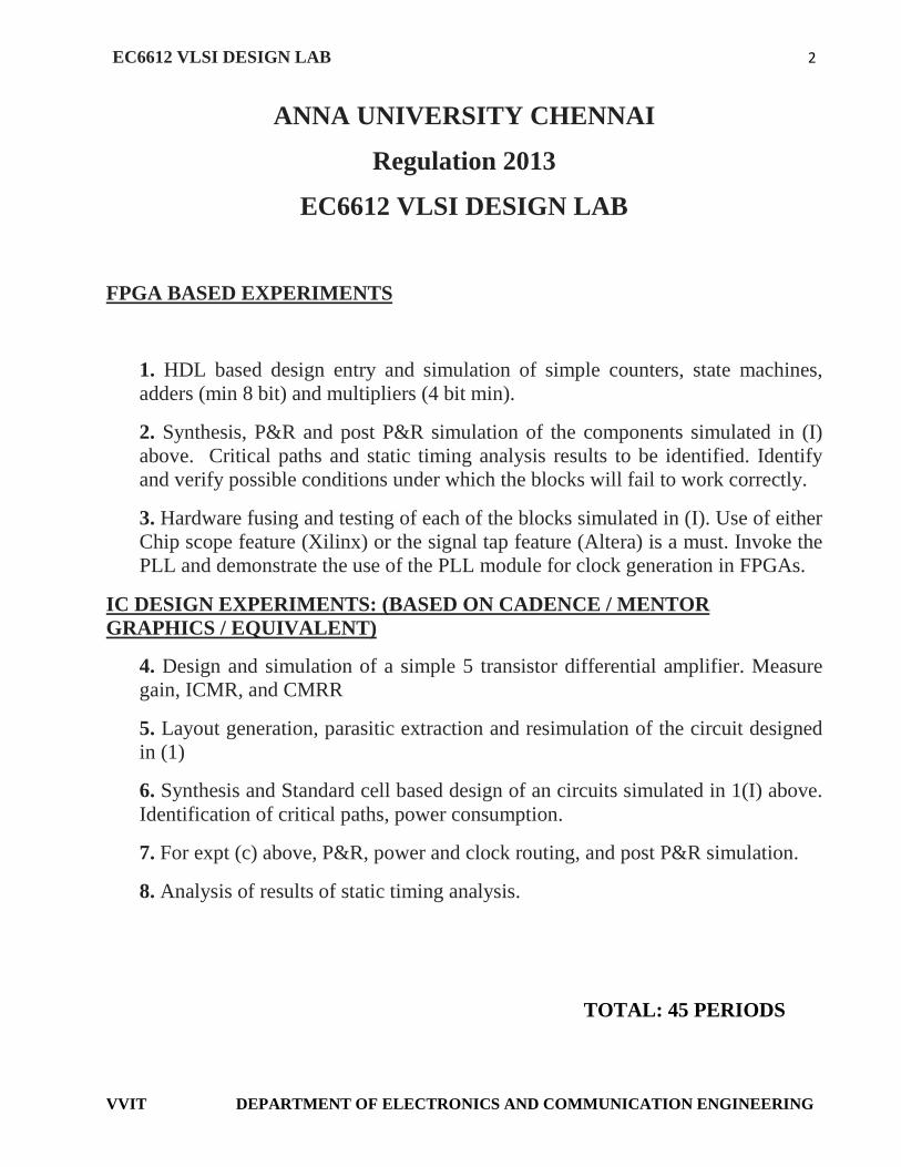
ANNA UNIVERSITY CHENNAI
Regulation 2013
EC6612 VLSI DESIGN LAB
FPGA BASED EXPERIMENTS
1. HDL based design entry and simulation of simple counters, state machines,adders (min 8 bit) and multipliers (4 bit min).
2. Synthesis, P&R and post P&R simulation of the components simulated in (I)above. Critical paths and static timing analysis results to be identified. Identifyand verify possible conditions under which the blocks will fail to work correctly.
3. Hardware fusing and testing of each of the blocks simulated in (I). Use of eitherChip scope feature (Xilinx) or the signal tap feature (Altera) is a must. Invoke thePLL and demonstrate the use of the PLL module for clock generation in FPGAs.
IC DESIGN EXPERIMENTS: (BASED ON CADENCE / MENTORGRAPHICS / EQUIVALENT)
4. Design and simulation of a simple 5 transistor differential amplifier. Measuregain, ICMR, and CMRR
5. Layout generation, parasitic extraction and resimulation of the circuit designedin (1)
6. Synthesis and Standard cell based design of an circuits simulated in 1(I) above.Identification of critical paths, power consumption.
7. For expt (c) above, P&R, power and clock routing, and post P&R simulation.
8. Analysis of results of static timing analysis.
TOTAL: 45 PERIODS
EC6612 VLSI DESIGN LAB 3
VVIT DEPARTMENT OF ELECTRONICS AND COMMUNICATION ENGINEERING
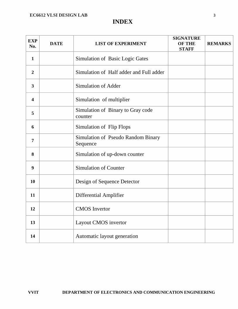
INDEX
EXPNo. DATE LIST OF EXPERIMENT
SIGNATUREOF THESTAFF
REMARKS
1 Simulation of Basic Logic Gates
2 Simulation of Half adder and Full adder
3 Simulation of Adder
4 Simulation of multiplier
5Simulation of Binary to Gray codecounter
6 Simulation of Flip Flops
7Simulation of Pseudo Random BinarySequence
8 Simulation of up-down counter
9 Simulation of Counter
10 Design of Sequence Detector
11 Differential Amplifier
12 CMOS Invertor
13 Layout CMOS invertor
14 Automatic layout generation
EC6612 VLSI DESIGN LAB 4
VVIT DEPARTMENT OF ELECTRONICS AND COMMUNICATION ENGINEERING
INTRODUCTION
Very-large-scale integration (VLSI) is the process of creating an integrated circuit (IC) by
combining thousands of transistors into a single chip. VLSI began in the 1970s when complex
semiconductor and communication technologies were being developed.
The microprocessor is a VLSI device. Before the introduction of VLSI technology most ICs
had a limited set of functions they could perform. An electronic circuit might consist of a CPU,
ROM, RAM and other glue logic. VLSI lets IC designers add all of these into one chip.
During the mid-1920s, several inventors attempted devices that were intended to control
current in solid-state diodes and convert them into triodes. Success did not come until after World
War II, during which the attempt to improve silicon and germanium crystals for use as radar
detectors led to improvements in fabrication and in the understanding of quantum mechanical states
of carriers in semiconductors.
Then scientists who had been diverted to radar development returned to solid-state device
development. With the invention of transistors at Bell Labs in 1947, the field of electronics shifted
from vacuum tubes to solid-state devices. With the small transistor at their hands, electrical
engineers of the 1950s saw the possibilities of constructing far more advanced circuits. As the
complexity of circuits grew, problems arose.
One problem was the size of the circuit. A complex circuit, like a computer, was dependent
on speed. If the components of the computer were too large or the wires interconnecting them too
long, the electric signals couldn't travel fast enough through the circuit, thus making the computer
too slow to be effective.
Jack Kilby at Texas Instruments found a solution to this problem in 1958. Kilby's idea was to
make all the components and the chip out of the same block (monolith) of semiconductor material.
Kilby presented his idea to his superiors, and was allowed to build a test version of his circuit.
In September 1958, he had his first integrated circuit ready. Although the first integrated
circuit was crude and had some problems, the idea was groundbreaking. By making all the parts out
of the same block of material and adding the metal needed to connect them as a layer on top of it,
there was no need for discrete components. No more wires and components had to be assembled
manually.
EC6612 VLSI DESIGN LAB 5
VVIT DEPARTMENT OF ELECTRONICS AND COMMUNICATION ENGINEERING
The circuits could be made smaller, and the manufacturing process could be automated From
here, the idea of integrating all components on a single silicon wafer came into existence, which led
to development in small-scale integration (SSI) in the early 1960s, medium-scale integration (MSI)
in the late 1960s, and then large-scale integration (LSI) as well as VLSI in the 1970s and 1980s, with
tens of thousands of transistors on a single chip (later hundreds of thousands, then millions, and now
billions (109).
The first semiconductor chips held two transistors each. Subsequent advances added more
transistors, and as a consequence, more individual functions or systems were integrated over time.
The first integrated circuits held only a few devices, perhaps as many as ten diodes, transistors,
resistors and capacitors, making it possible to fabricate one or more logic gates on a single device.
Now known retrospectively as small-scale integration (SSI), improvements in technique led to
devices with hundreds of logic gates, known as medium-scale integration (MSI). Further
improvements led to large-scale integration (LSI), i.e. systems with at least a thousand logic gates.
Current technology has moved far past this mark and today's microprocessors have many millions of
gates and billions of individual transistors.
At one time, there was an effort to name and calibrate various levels of large-scale
integration above VLSI. Terms like ultra-large-scale integration (ULSI) were used. But the huge
number of gates and transistors available on common devices has rendered such fine distinctions
moot. Terms suggesting greater than VLSI levels of integration are no longer in widespread use.

EC6612 VLSI DESIGN LAB 6
VVIT DEPARTMENT OF ELECTRONICS AND COMMUNICATION ENGINEERING
STEP BY STEP PROCESS FOR USING SIMULATION TOOLS
AIM:To study simulation tools using Xilinx software tool.
SOFTWARE REQUIRED:
1. Xilinx ISE Design Suite 14.1
PROCEDURE:
1. Now start the Xilinx ISE Design Suite 14.12. Go to file and click new project3. Enter the project name and click next4. Select the family name is Spartan 3E, speed is -4 and simulator is verilog click next
andclick Finish.5. Click new source.6. Select verilog module and type file name and click next.7. Assign input and output port and click next.8. Finally the report is shown click finish.9. Type the program save and click synthesis.10. To see the output wave form change the source from implementation to simulation
and click11. simulator behavior model in ISim simulator.12. Give values to the input variables and then click run13. In wave window, click run icon and you can see corresponding output.
Steps to use Xilinx tool:
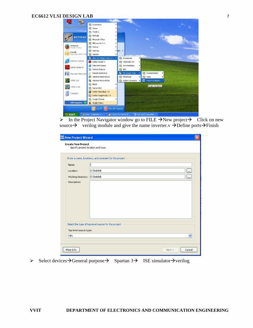
Start the Xilinx Project Navigator by using the desktop shortcut or by using theStartProgramsXilinx ISEProject Navigator.
EC6612 VLSI DESIGN LAB 7
VVIT DEPARTMENT OF ELECTRONICS AND COMMUNICATION ENGINEERING
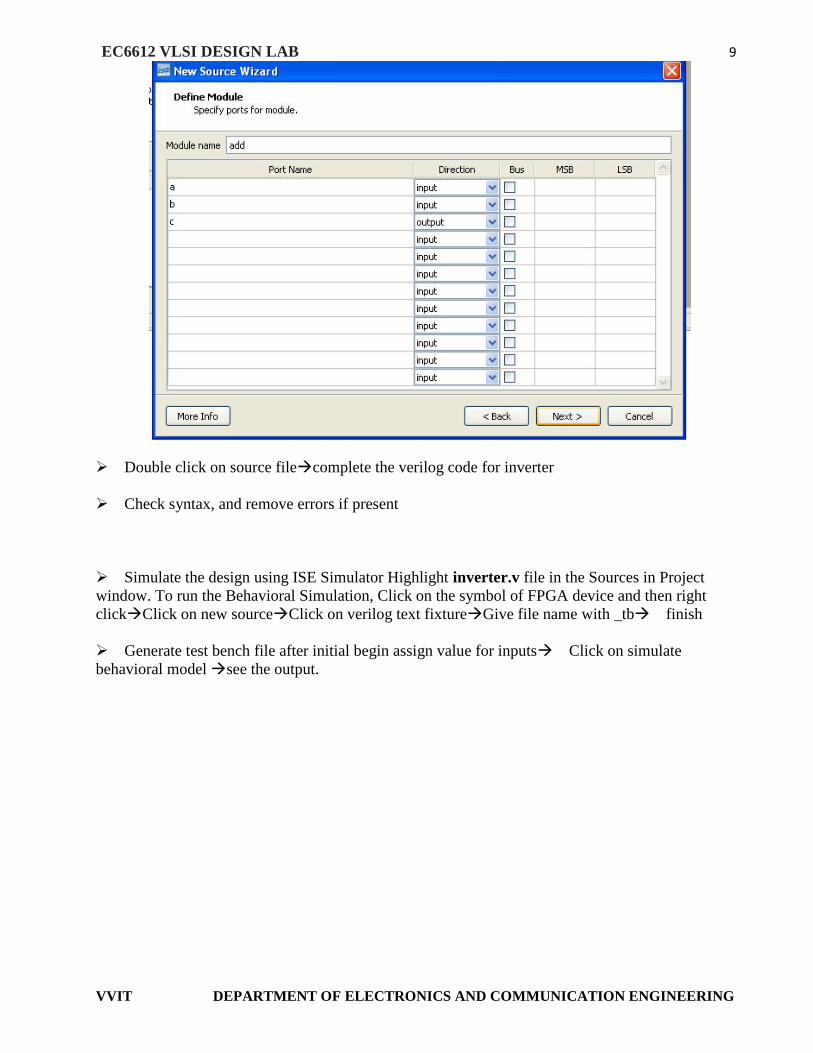
In the Project Navigator window go to FILENew projectClick on newsourceverilog module and give the name inverter.vDefine portsFinish
Select devicesGeneral purposeSpartan 3ISE simulatorverilog
EC6612 VLSI DESIGN LAB 8
VVIT DEPARTMENT OF ELECTRONICS AND COMMUNICATION ENGINEERING
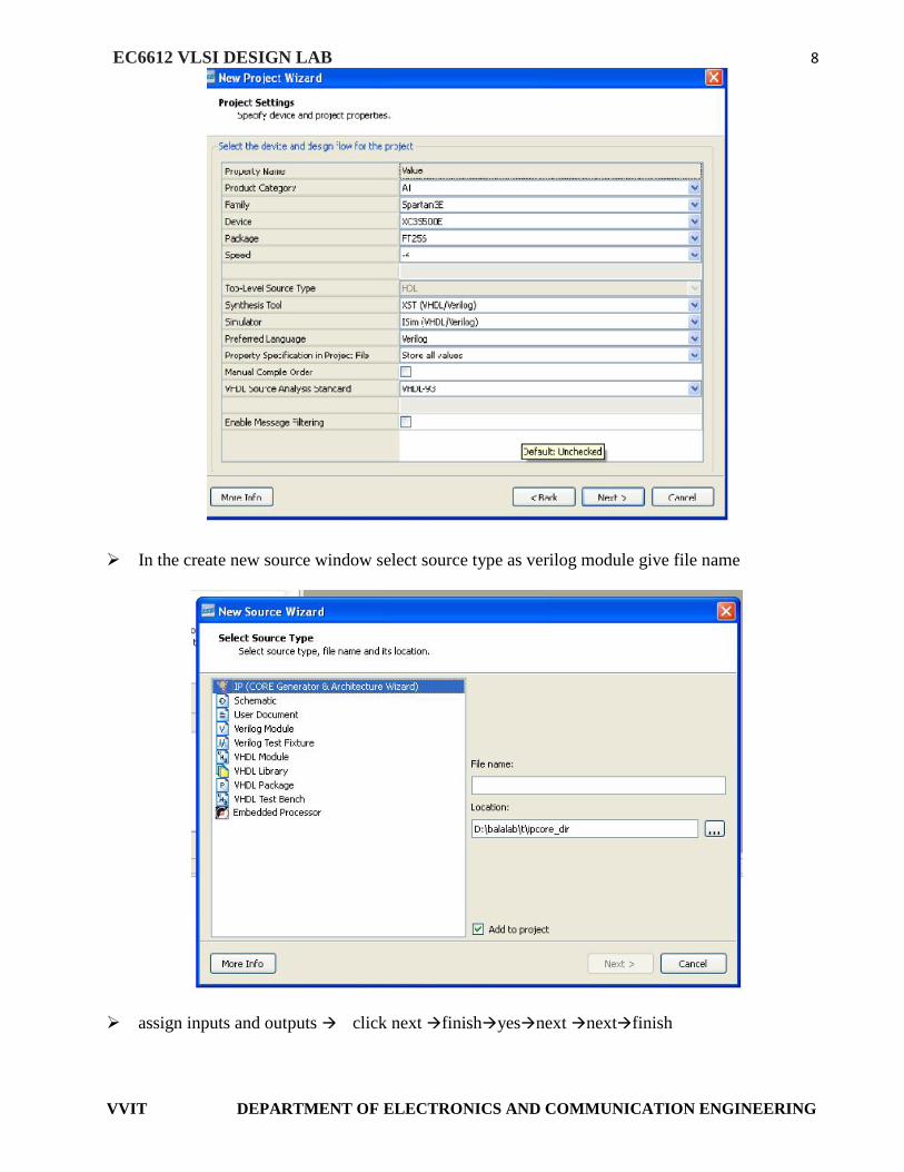
In the create new source window select source type as verilog module give file name
assign inputs and outputs click nextfinishyesnextnextfinish
EC6612 VLSI DESIGN LAB 9
VVIT DEPARTMENT OF ELECTRONICS AND COMMUNICATION ENGINEERING
Double click on source filecomplete the verilog code for inverter
Check syntax, and remove errors if present
Simulate the design using ISE Simulator Highlight inverter.v file in the Sources in Projectwindow. To run the Behavioral Simulation, Click on the symbol of FPGA device and then rightclickClick on new sourceClick on verilog text fixtureGive file name with _tbfinish
Generate test bench file after initial begin assign value for inputsClick on simulatebehavioral modelsee the output.

EC6612 VLSI DESIGN LAB 10
VVIT DEPARTMENT OF ELECTRONICS AND COMMUNICATION ENGINEERING
STEP BY STEP PROCESS FOR USING SYNTHESIZE TOOLS
SOFTWARE-.Xilinx ISE Design Suite 14.1
Synthesis is an automatic method of converting a higher level abstraction to a lower levelabstraction. The synthesis tool convert Register Transfer Level (RTL) description to gate levelnetlists.
These gate level netlists consist of interconnected gate level macro cells. These gate levelnetlists currently can be optimized for area, speed etc., The analyzed design is synthesized to alibrary of components, typically gates, latches, or flipflops. Hierarchical designs are synthesized inbottom up fashion, that is lower level components are synthesized before higher level components.Once the design is synthesized we have a gate level netlist. This gate level netlist can be simulated.Delay for the individual components are available as part of the description of the componentlibraries. Timing accurate simulation is not possible at this point because the actual timingcharacteristics are determined by the physical placement of the design within the FPGA chip.However, the functional simulation that is possible at this point is quite a bit more accurate thansimulation based on user specified delays. After run the synthesize in process window then full addermodel is converted to netlist file.
To convert the RTL to gates, three steps typically occur:
* The RTL description is translated to an unoptimized boolean description usually consistingof primitive gates such as AND and OR gates, flip-flop, and latches. This is a functionally correctbut completely unoptimized description.
* Boolean optimization algorithms are executed on this boolean equivalent description toproduce an optimized boolean equivalent description.
* This optimized boolean equivalent description is mapped to actual logic gate by makinguse of a technology library of the target process.
PROCEDURE:1. Now start the Xilinx ISE Design Suite 14.12. Go to file and click new project3. Enter the project name and click next4. Select the family name is Spartan 3E, speed is -4 and simulator is verilog click next andclick Finish.5. Click new source.6. Select verilog module and type file name and click next.7. Assign input and output port and click next.8. Finally the report is shown click finish.
EC6612 VLSI DESIGN LAB 11
VVIT DEPARTMENT OF ELECTRONICS AND COMMUNICATION ENGINEERING
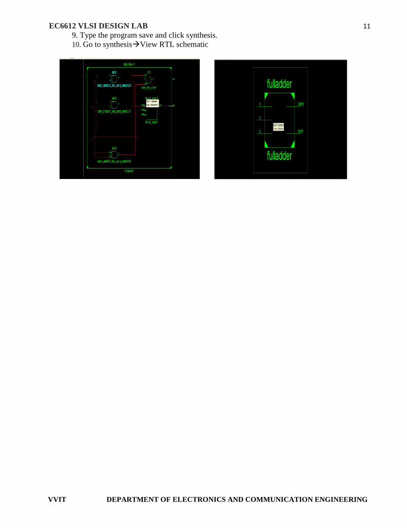
9. Type the program save and click synthesis.10. Go to synthesisView RTL schematic
EC6612 VLSI DESIGN LAB 12
VVIT DEPARTMENT OF ELECTRONICS AND COMMUNICATION ENGINEERING
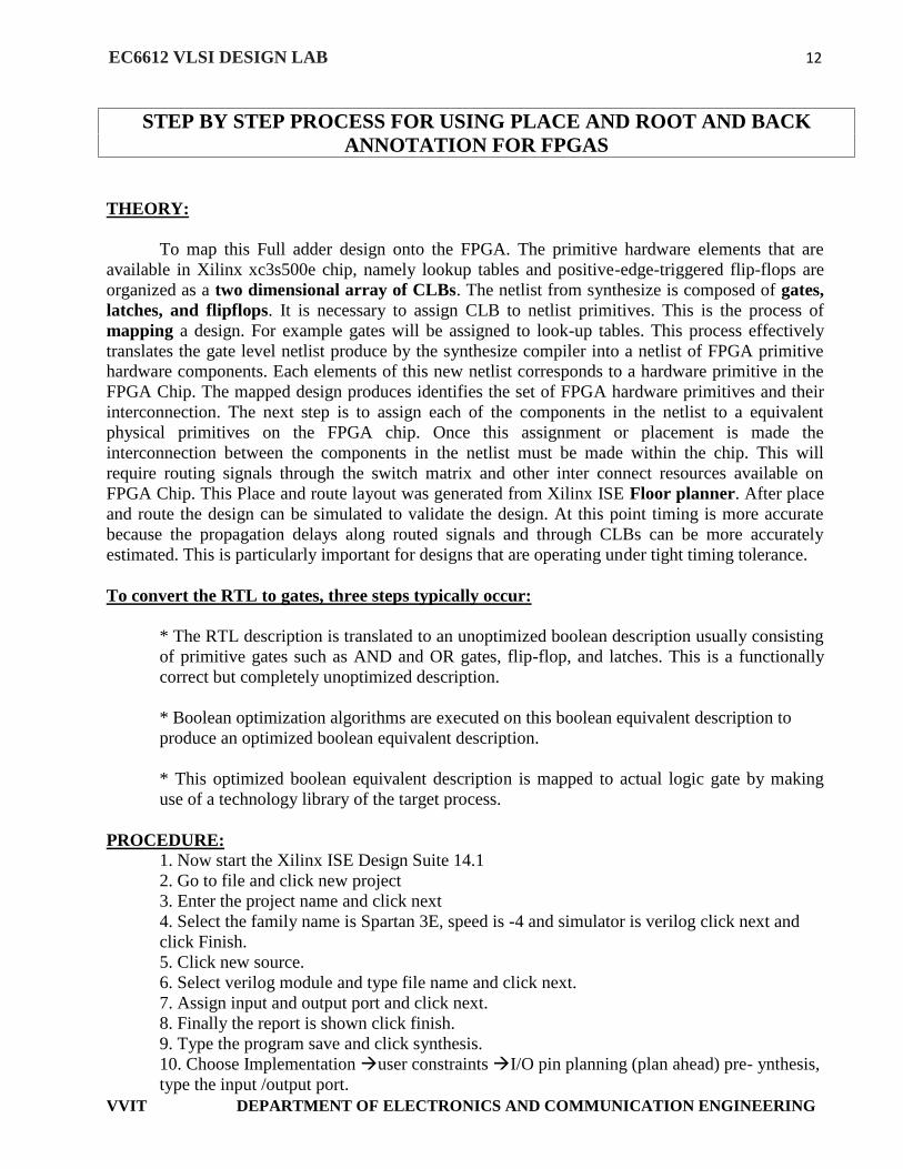
STEP BY STEP PROCESS FOR USING PLACE AND ROOT AND BACKANNOTATION FOR FPGAS
THEORY:
To map this Full adder design onto the FPGA. The primitive hardware elements that areavailable in Xilinx xc3s500e chip, namely lookup tables and positive-edge-triggered flip-flops areorganized as a two dimensional array of CLBs. The netlist from synthesize is composed of gates,latches, and flipflops. It is necessary to assign CLB to netlist primitives. This is the process ofmapping a design. For example gates will be assigned to look-up tables. This process effectivelytranslates the gate level netlist produce by the synthesize compiler into a netlist of FPGA primitivehardware components. Each elements of this new netlist corresponds to a hardware primitive in theFPGA Chip. The mapped design produces identifies the set of FPGA hardware primitives and theirinterconnection. The next step is to assign each of the components in the netlist to a equivalentphysical primitives on the FPGA chip. Once this assignment or placement is made theinterconnection between the components in the netlist must be made within the chip. This willrequire routing signals through the switch matrix and other inter connect resources available onFPGA Chip. This Place and route layout was generated from Xilinx ISE Floor planner. After placeand route the design can be simulated to validate the design. At this point timing is more accuratebecause the propagation delays along routed signals and through CLBs can be more accuratelyestimated. This is particularly important for designs that are operating under tight timing tolerance.
To convert the RTL to gates, three steps typically occur:
* The RTL description is translated to an unoptimized boolean description usually consistingof primitive gates such as AND and OR gates, flip-flop, and latches. This is a functionallycorrect but completely unoptimized description.
* Boolean optimization algorithms are executed on this boolean equivalent description toproduce an optimized boolean equivalent description.
* This optimized boolean equivalent description is mapped to actual logic gate by makinguse of a technology library of the target process.
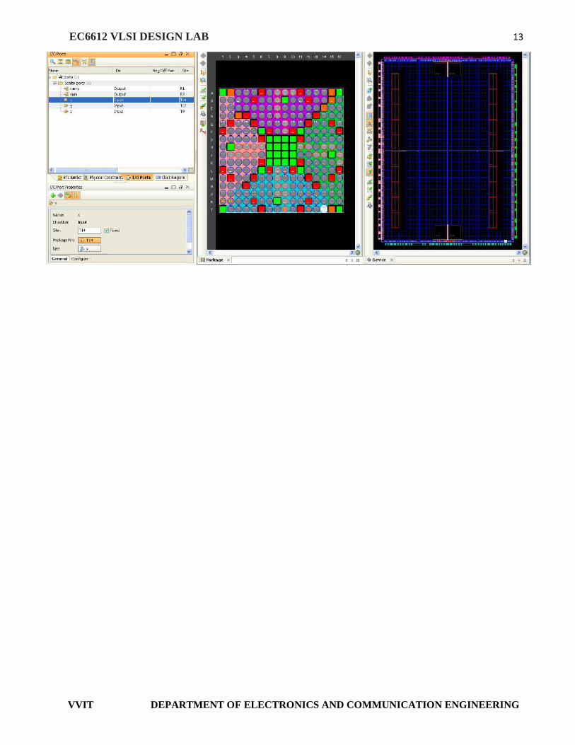
PROCEDURE:1. Now start the Xilinx ISE Design Suite 14.12. Go to file and click new project3. Enter the project name and click next4. Select the family name is Spartan 3E, speed is -4 and simulator is verilog click next andclick Finish.5. Click new source.6. Select verilog module and type file name and click next.7. Assign input and output port and click next.8. Finally the report is shown click finish.9. Type the program save and click synthesis.10. Choose Implementationuser constraintsI/O pin planning (plan ahead) pre- ynthesis,type the input /output port.
EC6612 VLSI DESIGN LAB 13
VVIT DEPARTMENT OF ELECTRONICS AND COMMUNICATION ENGINEERING
EC6612 VLSI DESIGN LAB 14
VVIT DEPARTMENT OF ELECTRONICS AND COMMUNICATION ENGINEERING
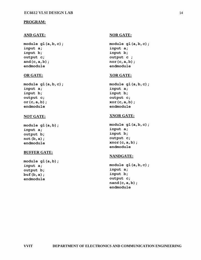
PROGRAM:
AND GATE:
module gl(a,b,c);input a;input b;output c;and(c,a,b);endmodule
OR GATE:
module gl(a,b,c);input a;input b;output c;or(c,a,b);endmodule
NOT GATE:
module gl(a,b);input a;output b;not(b,a);endmodule
BUFFER GATE:
module gl(a,b);input a;output b;buf(b,a);endmodule
NOR GATE:
module gl(a,b,c);input a;input b;output c ;nor(c,a,b);endmodule
XOR GATE:
module gl(a,b,c);input a;input b;output c;xor(c,a,b);endmodule
XNOR GATE:
module gl(a,b,c);input a;input b;output c;xnor(c,a,b);endmodule
NANDGATE:
module gl(a,b,c);input a;input b;output c;nand(c,a,b);endmodule
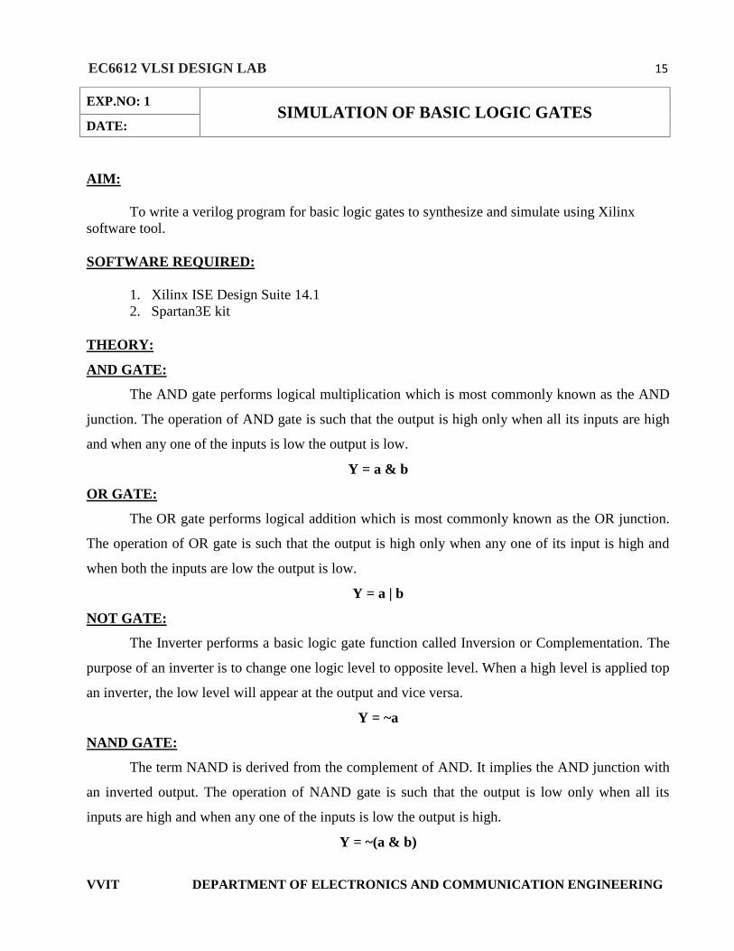
EC6612 VLSI DESIGN LAB 15
VVIT DEPARTMENT OF ELECTRONICS AND COMMUNICATION ENGINEERING
AIM:
To write a verilog program for basic logic gates to synthesize and simulate using Xilinxsoftware tool.
SOFTWARE REQUIRED:
1. Xilinx ISE Design Suite 14.12. Spartan3E kit
THEORY:
AND GATE:
The AND gate performs logical multiplication which is most commonly known as the AND
junction. The operation of AND gate is such that the output is high only when all its inputs are high
and when any one of the inputs is low the output is low.
Y = a & b
OR GATE:
The OR gate performs logical addition which is most commonly known as the OR junction.
The operation of OR gate is such that the output is high only when any one of its input is high and
when both the inputs are low the output is low.
Y = a | b
NOT GATE:
The Inverter performs a basic logic gate function called Inversion or Complementation. The
purpose of an inverter is to change one logic level to opposite level. When a high level is applied top
an inverter, the low level will appear at the output and vice versa.
Y = ~a
NAND GATE:
The term NAND is derived from the complement of AND. It implies the AND junction with
an inverted output. The operation of NAND gate is such that the output is low only when all its
inputs are high and when any one of the inputs is low the output is high.
Y = ~(a & b)
EXP.NO: 1SIMULATION OF BASIC LOGIC GATES
DATE:

EC6612 VLSI DESIGN LAB 16
VVIT DEPARTMENT OF ELECTRONICS AND COMMUNICATION ENGINEERING
NOR GATE:
The term NOR is derived from the complement of OR. It implies the OR junction with an
inverted output. The operation of NOR gate is such that the output is high only when all its inputs
are low and when any one of the inputs is high the output is low.
Y = ~(a | b)
EX-OR GATE:
The output is high only when the inputs are at opposite level.
Y = a ^ b
EX-NOR GATE:
The output is high only when the inputs are at same level.
Y = ~(a ^ b)
RESULT:
Thus the basic logic gates verilog program for to synthesize and simulate using Xilinx
software tool was verified.

EC6612 VLSI DESIGN LAB 17
VVIT DEPARTMENT OF ELECTRONICS AND COMMUNICATION ENGINEERING
PROGRAM:(SIMULATION OF HALF ADDER AND FULL ADDER)
HALF ADDER
modulehalfadder(a,b,sum,carry);input a,b;output sum,carry;xor(sum,a,b);and(carry,a,b);endmodule
FULL ADDER
module full_adder(a,b,c,sum,carry);output sum,carry ;input a,b,c ;assign sum = a ^ b ^ c;assign carry = (a&b) | (b&c) |(c&a);endmoduleBEHAVIORAL MODELLING:
module full_adder(a,b,c,sum,carry);output sum,carry;reg sum,carry;input a,b,c;always @(a,b,c)beginsum=a^b^c;carry=(a&b)|(b&c)|(c&a);end
endmodule
STRUCURAL MODELLING:
modulefull_adder(sum,carry,a,b,c);input a,b,c;output sum,carry;wire w1,w2,w3;xor x1(w1,a,b);xor x2(sum,w1,c);and a1(w2,a,b);and a2(w3,w1,c);or(carry,w2,w3);endmodule
FULL ADDER USING HALF ADDER
module half_adder(x,y,s,c);input x,y;output s,c;xor(s,x,y);and(c,x,y);endmodulemodulefull_adder(x,y,cin,s,cout);input x,y,cin;output s,cout;wire s1,c1,c2;half_adder ha1(x,y,s1,c1);half_adder ha2(cin,s1,s,c2);or(cout,c1,c2);endmodule
EC6612 VLSI DESIGN LAB 18
VVIT DEPARTMENT OF ELECTRONICS AND COMMUNICATION ENGINEERING
AIM:To write a verilog program for half adder and full adder to synthesize and simulate using
Xilinx software tool.
SOFTWARE REQUIRED:
1. Xilinx ISE Design Suite 14.12. Spartan3E kit
THEORY:
HALF ADDER:
The half adder consists of two input variables designated as Augends and Addend bits.Output variables produce the Sum and Carry. The „carry‟ output is 1 only when both inputs are 1and ,sum‟ is 1 if any one input is 1. The Boolean expression is given by,
sum = x ^ ycarry = x & y
FULL ADDER:
A Full adder is a combinational circuit that focuses the arithmetic sum of three bits. Itconsists of 3 inputs and 2 outputs. The third input is the carry from the previous Lower SignificantPosition. The two outputs are designated as Sum (S) and Carry (C). The binary variable S gives thevalue of the LSB of the Sum. The output S=1 only if odd number of 1‟s are present in the input andthe output C=1 if two or three inputs are 1.
sum = x ^ y ^ zcarry= (x & y) | (y & z) | (x & z)
PROCEDURE:
1. Click on the Xilinx ISE Design Suite 14.1or Xilinx Project navigator icon on the desktop
of PC.
2. Write the Verilog code by choosing HDL as top level source module.
3. Check syntax, view RTL schematic and note the device utilization summary by double
clicking on the synthesis in the process window.
4. Perform the functional simulation using Xilinx ISE simulator.
5. The output can be observed by using model sim.
EXP.NO: 2SIMULATION OF HALF ADDER AND FULL ADDER
DATE:

EC6612 VLSI DESIGN LAB 19
VVIT DEPARTMENT OF ELECTRONICS AND COMMUNICATION ENGINEERING
RESULT
Thus the for half adder and full adder verilog program for to synthesize and simulate using
Xilinx software tool was verified.

EC6612 VLSI DESIGN LAB 20
VVIT DEPARTMENT OF ELECTRONICS AND COMMUNICATION ENGINEERING
PROGRAM:(SIMULATION OF ADDER)
4-BIT ADDER
module adder4(a,b,c,sum,Cout);input [3:0]a,b;input c;output [3:0]sum;output Cout;assign {Cout,sum}=a+b+c;endmoduleADDITION OF TWO 8-BITNUMBERS
module adder(a,b, sum,carry);input [7:0]a,b;output [7:0]sum,carry;assign {carry,sum}=a+b;endmodule
ADDITION OF FOUR 8-BITNUMBERS
moduleadder(a,b,c,d,sum,carry);input [7:0]a,b,c,d;output [7:0]sum,carry;assign {carry,sum}=a+b+c+d;endmodule
8-BIT RIPPLE CARRY ADDER
module fulladd(a, b, cin, sum,cout);input a,b,cin;output sum, cout;assign sum=(a^b^cin);assigncout=((a&b)|(b&cin)|(a&cin));endmodule
module ripplemod(a, b, cin,sum, cout);input [7:0] a,b;input cin;
output [7:0]sum;output cout;wire[6:0] c;fulladda1(a[0],b[0],cin,sum[0],c[0]);fulladda2(a[1],b[1],c[0],sum[1],c[1]);fulladda3(a[2],b[2],c[1],sum[2],c[2]);fulladda4(a[3],b[3],c[2],sum[3],c[3]);fulladda5(a[4],b[4],c[3],sum[4],c[4]);fulladda6(a[5],b[5],c[4],sum[5],c[5]);fulladda7(a[6],b[6],c[5],sum[6],c[6]);fulladda8(a[7],b[7],c[6],sum[7],cout);endmodule
4-BIT RIPPLE CARRY ADDER
module fulladd(a, b, cin, sum,cout);input a,b,cin;output sum,cout;assign sum=(a^b^cin);assigncout=((a&b)|(b&cin)|(a&cin));endmodulemodule ripplemod(a, b, cin,sum, cout);input [3:0]a,b;input cin;output [3:0]sum;output cout;wire[2:0] c;fulladda1(a[0],b[0],cin,sum[0],c[0]);fulladda2(a[1],b[1],c[0],sum[1],c[1]);fulladda3(a[2],b[2],c[1],sum[2],c[2]);fulladda4(a[3],b[3],c[2],sum[3],cout);endmodule

EC6612 VLSI DESIGN LAB 21
VVIT DEPARTMENT OF ELECTRONICS AND COMMUNICATION ENGINEERING
AIM:
To write a verilog program for Adder to synthesize and simulate using Xilinx software tool.
SOFTWARE REQUIRED:
1. Xilinx ISE Design Suite 14.12. Spartan3E kit
THEORY :
When you add large numbers carefully together the addition is done digit by digit. The
comwter does the same. In the illustration, two 8 –digit binary numbers are being added. The top
row contains the first number and the second row the other. Working from the right-hand side, there
can be no 'carry' to acd to the sum of the first two digits, so a half adder is sufficient. But for the
second and subsequent pairs of digits, full adders must be usee (any carry' is indicated by a f below
the adder). The output will be an 8- bit and if the carry is formed that will be shown in cout output
value.
PROCEDURE:
1. Click on the Xilinx ISE Design Suite 14.1or Xilinx Project navigator icon on the desktop
of PC.
2. Write the Verilog code by choosing HDL as top level source module.
3. Check syntax, view RTL schematic and note the device utilization summary by double
4. clicking on the synthesis in the process window.
5. Perform the functional simulation using Xilinx ISE simulator.
6. The output wave form can be observed in model sim.
RESULT:
Thus the for Adder verilog program for to synthesize and simulate using Xilinx software tool
was verified.
EXP.NO: 3SIMULATION OF ADDERDATE:

EC6612 VLSI DESIGN LAB 22
VVIT DEPARTMENT OF ELECTRONICS AND COMMUNICATION ENGINEERING
PROGRAM:(SIMULATION OF MULTIPLIER)
MULTIPLICATION OF TWO 4-BITNUMBERS / 4-BIT MULTIPLIER
module adder(a,b, out);input [3:0]a,b;output [7:0]out;assign out= a*b;endmodule
BOOTHS MULTIPLIER (4-BITMULTIPLIER)
module bm(xa,ya,za);input [3:0]xa;input [3:0]ya;output [7:0]za;integer i;reg[9:0]temp;reg[1:0]a;reg[5:0]y;reg[5:0]x;reg[9:0]z;reg[7:0]za;always@ (xa or ya)beginy[5:0]=6'b000000;y[5:1]=ya[3:0];x[4:0]=xa[3:0];z=9'b000000000;temp=10'b0000000000;for(i=0;i<=4;i=i+1)begina[0]=y[i];a[1]=y[i+1];case(a)2'b01:temp[4:0]=x[4:0];
2'b10:temp[4:0]=(~x[4:0])+5'b0001;2'b11:temp[4:0]=5'b00000;2'b00:temp[4:0]=5'b00000;endcaseif(temp[4]==0)begintemp[9:5]=5'b00000;endelsebegintemp[9:5]=5'b11111;endtemp=temp<<i;z=z+temp;endza=z;endendmodule

EC6612 VLSI DESIGN LAB 23
VVIT DEPARTMENT OF ELECTRONICS AND COMMUNICATION ENGINEERING
AIM:To write a verilog program for multiplier to synthesize and simulate using Xilinx software
tool.
SOFTWARE REQUIRED:
1. Xilinx ISE Design Suite 14.12. Spartan3E kit.
THEORY:
Multiplication of two elements in the polynomial basis can be accomplished in the normal
way of multiplication, but there are a number of ways to speed up multiplication, especially in
hardware. In this type the multiplication can done parallel counter and it is generate carry. The
multiplication is independent of the carry so we can perform N number of multiplication
independent of carry.
PROCEDURE:
1. Click on the Xilinx ISE Design Suite 14.1or Xilinx Project navigator icon on the
desktop of PC.
2. Write the Verilog code by choosing HDL as top level source module.
3. Check syntax, view RTL schematic and note the device utilization summary by
double
4. Clicking on the synthesis in the process window.
5. Perform the functional simulation using Xilinx ISE simulator.
6. The output wave form can be observed in model sim.
RESULT:
Thus the for multiplier verilog program for to synthesize and simulate using Xilinx software
tool was verified.
EXP.NO: 4SIMULATION OF MULTIPLIERDATE:

EC6612 VLSI DESIGN LAB 24
VVIT DEPARTMENT OF ELECTRONICS AND COMMUNICATION ENGINEERING
PROGRAM:
SIMULATION OF BINARY TO GRAY CODE CONVERSION:
module btog(din,dout);output [3:0]dout;input [3:0]din;assign dout[3]=din[3];assign dout[2]=din[3]^din[2];assign dout[1]=din[2]^din[1];assign dout[0]=din[1]^din[0];endmodule
EC6612 VLSI DESIGN LAB 25
VVIT DEPARTMENT OF ELECTRONICS AND COMMUNICATION ENGINEERING
AIM:
To write a verilog program for D-flip flop and D-latch to synthesize and simulate usingxilinx software tool.
SOFTWARE REQUIRED:
1. Xilinx ISE Design Suite 14.12. Spartan3E kit
THEORY:
CODE CONVERTOR:
Code is a symbolic representation of discrete information. Codes are of different types. GrayCode is one of the most important codes. It is a non-weighted code which belongs to a class of codescalled minimum change codes. In this codes while traversing from one step to another step only onebit in the code group changes. In case of Gray Code two adjacent code numbers differs from eachother by only one bit. As this code it is not applicable in any types of arithmetical operations but ithas some applications in analog to digital converters and in some input/output devices. Now let usconcentrate on the table of Gray Code given below where we can find the difference of binary codefrom gray code while traversing through the table for their respective decimal numbers.
BINARY TO GRAY CODE CONVERSION:
Binary to gray code conversion is a very simple process. There are several steps to do thistypes of conversions. Steps given below elaborate on the idea on this type of conversion.
(1) The M.S.B. of the gray code will be exactly equal to the first bit of the given binarynumber.
(2) Now the second bit of the code will be exclusive-or of the first and second bit of thegiven binary number, i.e if both the bits are same the result will be 0 and if they aredifferent the result will be 1.
(3) The third bit of gray code will be equal to the exclusive-or of the second and third bitof the given binary number. Thus the Binary to gray code conversion goes on. Oneexample given below can make your idea clear on this type of conversion.
EXP.NO: 5SIMULATION OF BINARY TO GRAY CODE COUNTERDATE:

EC6612 VLSI DESIGN LAB 26
VVIT DEPARTMENT OF ELECTRONICS AND COMMUNICATION ENGINEERING
Let (01001) be the given binary number Thus the equivalent gray code is 01101.
Now concentrate on the example where the M.S.B. of the binary is 0 so for it will be 0 forthe most significant gray bit. Next, the XOR of the first and the second bit is done. The bits aredifferent so the resultant gray bit will be 1. Again move to the next step, XOR of second and third bitis again 1 as they are different. Next, XOR of third and fourth bit is 0 as both the bits are same.Lastly the XOR of fourth and fifth bit is 1 as they are different. That is how the result of binary togray code conversion of 01001 is done whose equivalent gray code is 01101.
PROCEDURE:
1. Click on the Xilinx ISE Design Suite 14.1or Xilinx Project navigator icon on the desktop of
PC.
2. Write the Verilog code by choosing HDL as top level source module.
3. Check syntax, view RTL schematic and note the device utilization summary by double
clicking on the synthesis in the process window.
4. Perform the functional simulation using Xilinx ISE simulator.
5. The output can be observed using model sim.
RESULT:
Thus the for multiplier verilog program for to synthesize and simulate using Xilinx software
tool was verified.

EC6612 VLSI DESIGN LAB 27
VVIT DEPARTMENT OF ELECTRONICS AND COMMUNICATION ENGINEERING
PROGRAM:
(SIMULATION OF FLIP FLOPS)
D LATCH:
moduledlatch(d,en,b,c,a,q,qbar);input d,en;output b,c,a,q,qbar;wire b,c,a,q,qbar;not(a,d);nand(b,d,en);nand(c,a,en);nand(q,b,qbar);nand(qbar,c,q);endmodule
JK FLIP FLOP:module JK_Flip_Flop(Q,Qbar,clk,reset,J,K);output Q,Qbar;input clk, reset,J,K;reg Q;always @(posedge clk)if (reset)beginQ <= 0;endelse if (J == 0 && K == 0)beginQ <= Q;endelse if (J == 0 && K == 1)beginQ <= 0;endelse if (J == 1 && K == 0)beginQ <= 1;endelse if (J == 1 && K == 1)
beginQ <= Qbar;endassign Qbar = ~Q;endmodule
SR FLIP FLOP:
module SR_Flip_Flop(Q,Qbar,clk,reset,S,R);output Q,Qbar;input clk, reset,S,R;reg Q;always @(posedge clk)if (reset)beginQ <= 0;endelse if (S == 0 && R == 0)beginQ <= Q;endelse if (S == 0 && R == 1)beginQ <= 0;endelse if (S == 1 && R == 0)beginQ <= 1;endelse if (S == 1 && R == 1)beginQ <= 1'bx;endassign Qbar = ~Q;endmodule

EC6612 VLSI DESIGN LAB 28
VVIT DEPARTMENT OF ELECTRONICS AND COMMUNICATION ENGINEERING
AIM:
To write a verilog program for various flip flops to synthesize and simulate using Xilinxsoftware tool.
SOFTWARE REQUIRED:
1. Xilinx ISE Design Suite 14.12. Spartan3E kit
THEORY:
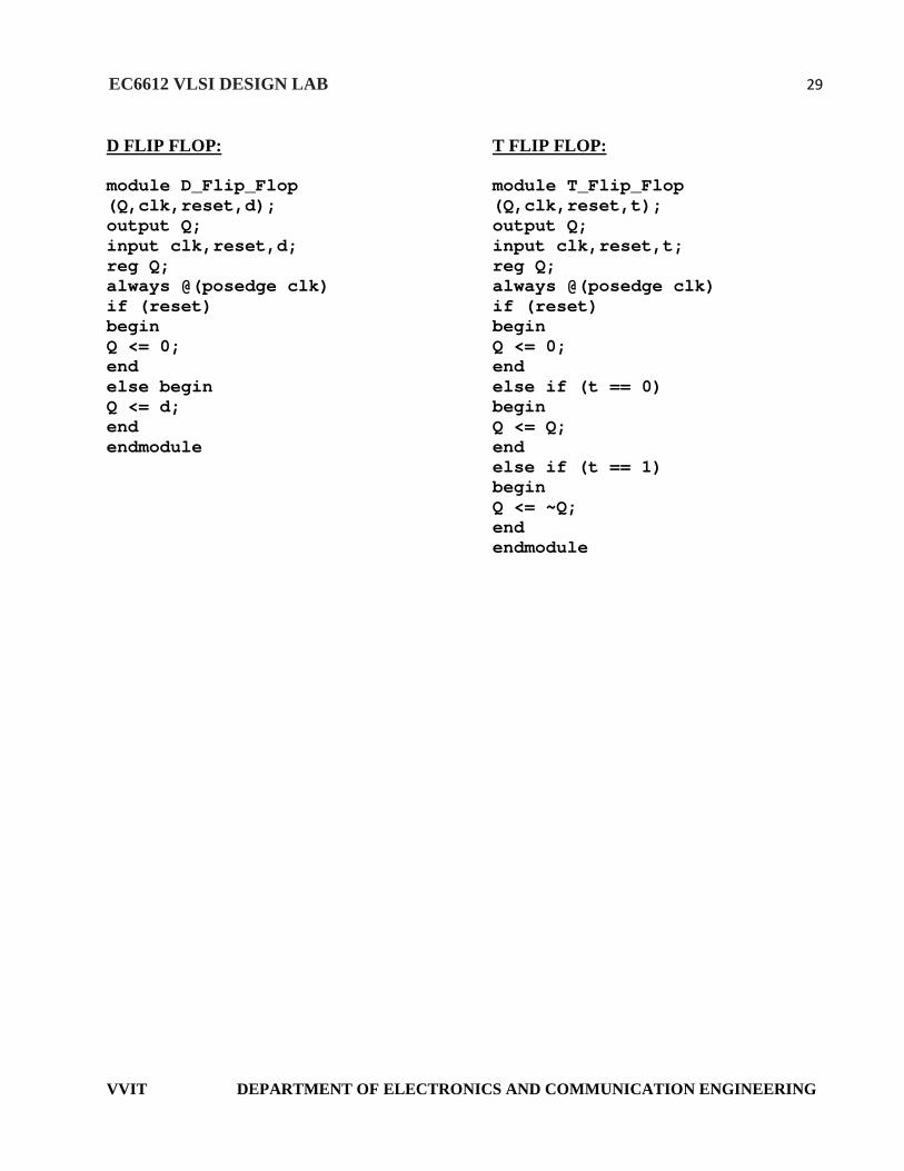
D-FLIP FLOP:
It has only a single data input. That data input is connected to the S input of RS-flip flop,
while the inverse of D is connected to the R input. This prevents that the input combination ever
occurs. To allow the flip flop to be in holding state, a D-flip flop has a second input called “clock”.
The clock input is AND-ed with the D input, such that when clock=0, the R and S inputs of the RS-
flip flop are 0 and the state is held.
D-LATCH:
It has only a single data input. That data input is connected to the S input of RS-flip flop,
while the inverse of D is connected to the R input. This prevents that the input combination ever
occurs. To allow the flip flop to be in holding state, a D-flip flop has a second input called “enable”.
The enable input is AND-ed with the D input, such that when enable=0, the R and S inputs of the
RS-flip flop are 0 and the state is held.
EXP.NO: 6SIMULATION OF FLIP FLOPSDATE:
EC6612 VLSI DESIGN LAB 29
VVIT DEPARTMENT OF ELECTRONICS AND COMMUNICATION ENGINEERING
D FLIP FLOP:
module D_Flip_Flop(Q,clk,reset,d);output Q;input clk,reset,d;reg Q;always @(posedge clk)if (reset)beginQ <= 0;endelse beginQ <= d;endendmodule
T FLIP FLOP:
module T_Flip_Flop(Q,clk,reset,t);output Q;input clk,reset,t;reg Q;always @(posedge clk)if (reset)beginQ <= 0;endelse if (t == 0)beginQ <= Q;endelse if (t == 1)beginQ <= ~Q;endendmodule
EC6612 VLSI DESIGN LAB 30
VVIT DEPARTMENT OF ELECTRONICS AND COMMUNICATION ENGINEERING
PROCEDURE:
1. Click on the Xilinx ISE Design Suite 14.1or Xilinx Project navigator icon on the
desktop of PC.
2. Write the Verilog code by choosing HDL as top level source module.
3. Check syntax, view RTL schematic and note the device utilization summary by
double clicking on the synthesis in the process window.
4. Perform the functional simulation using Xilinx ISE simulator.
5. The output can be observed using model sim
RESULT:
Thus the various flip flops verilog program for to synthesize and simulate using Xilinx
software tool was verified.

EC6612 VLSI DESIGN LAB 31
VVIT DEPARTMENT OF ELECTRONICS AND COMMUNICATION ENGINEERING
PROGRAM:
PSEUDO RANDOM BINARY SEQUENCE (4-BIT):
module tff(q,t,c);output q;input t,c;reg q;initialbeginq=1'b1;endalways @ (posedge c)beginif (t==1'b0) begin q=q; endelse begin q=~q; endendendmodulemodule tff1(q,t,c);output q;input t,c;reg q;initialbegin
q=1'b0;endalways @ (posedge c)beginif (t==1'b0) begin q=q; endelse begin q=~q; endendendmodulemodule random(o,clk);output [3:0]o;input clk;xor (t0,o[3],o[2]);assign t1=o[0];assign t2=o[1];assign t3=o[2];tff u1(o[0],t0,clk);tff1 u2(o[1],t1,clk);tff1 u3(o[2],t2,clk);tff1 u4(o[3],t3,clk);endmodule

EC6612 VLSI DESIGN LAB 32
VVIT DEPARTMENT OF ELECTRONICS AND COMMUNICATION ENGINEERING
AIM:
To write a verilog program for Pseudo Random Binary Sequence to synthesize and simulateusing Xilinx software tool.
SOFTWARE REQUIRED:
1. Xilinx ISE Design Suite 14.12. Spartan3E kit
THEORY :
PRBS :
A PRBS is 'pseudorandom', because, although it is in fact deterministic, it seems to berandom in a sense that the value of an element is independent of the values of any of the otherelements, similar to real random sequences. A PRBS can be stretched to infinity by repeating it afterelements, this in contrast to most random sequences, such as sequences generated by radioactivedecay or by white noise, that are 'infinite' by nature. The PRBS is more general than the maximumlength sequence, which is a special pseudo-random binary sequence of N bits generated as the outputof a linear shift register. A maximum length sequence always has a 1/2 duty cycle and its number ofelements .
PROCEDURE:
1. Click on the Xilinx ISE Design Suite 14.1or Xilinx Project navigator icon on thedesktop of PC.
2. Write the Verilog code by choosing HDL as top level source module.3. Check syntax, view RTL schematic and note the device utilization summary by
double4. clicking on the synthesis in the process window.5. Perform the functional simulation using Xilinx ISE simulator.6. The output wave form can be observed in model sim.
RESULT:
Thus the various flip flops verilog program for to synthesize and simulate using Xilinx
software tool was verified.
EXP.NO: 7SIMULATION OF PSEUDO RANDOM BINARY SEQUENCEDATE:

EC6612 VLSI DESIGN LAB 33
VVIT DEPARTMENT OF ELECTRONICS AND COMMUNICATION ENGINEERING
PROGRAM:
UP-DOWN COUNTER:
module updowncounterm(clk, clear, updown, q);input clk;input clear;input updown;output [3:0] q;reg [3:0] q;always@(posedge clear or posedge clk)beginif(clear)q <=4'b0000;else if(updown)q <= q+1'b1;elseq <= q-1'b1;endendmodule

EC6612 VLSI DESIGN LAB 34
VVIT DEPARTMENT OF ELECTRONICS AND COMMUNICATION ENGINEERING
AIM:
To write a verilog program for Up-Down Counter to synthesize and simulate using Xilinxsoftware tool.
SOFTWARE REQUIRED:
1. Xilinx ISE Design Suite 14.12. Spartan3E kit
THEORY :
UP-DOWN COUNTER :
A counter that can change state in either direction, under the control of an up or down
selector input, is known as an up/down counter. When the selector is in the up state, the counter
increments its value. When the selector is in the down state, the counter decrements the count.
Likewise the counter counts in both the directions continuously until attaining the end of the count.
The count is initiated by the positive clock pulse. The counter counts from 0000 to 1111 for up count
and 1111 to 0000 for down count.
PROCEDURE:
1. Click on the Xilinx ISE Design Suite 14.1or Xilinx Project navigator icon on the
desktop of PC.
2. Write the Verilog code by choosing HDL as top level source module.
3. Check syntax, view RTL schematic and note the device utilization summary by
double clicking on the synthesis in the process window.
4. Perform the functional simulation using Xilinx ISE simulator.
5. The output wave form can be observed in model sim.
RESULT:
Thus the Up-Down Counter verilog program for to synthesize and simulate using Xilinx
software tool was verified.
EXP.NO: 8SIMULATION OF UP-DOWN COUNTERDATE:

EC6612 VLSI DESIGN LAB 35
VVIT DEPARTMENT OF ELECTRONICS AND COMMUNICATION ENGINEERING
PROGRAM:
MOD 10 COUNTER / DECADE COUNTER:
module counter(clk,rst,enable,counter_output);input clk,rst,enable;output reg [3:0]counter_output;always@ (posedge (clk))beginif( rst | counter_output==4'b1001)counter_output <= 4'b0000;else if(enable)counter_output <= counter_output + 1;elsecounter_output <= 4'b0000;endendmodule
MOD 12 COUNTER:
module counter(clk,rst,enable,counter_output);input clk,rst,enable;output reg [3:0]counter_output;always@ (posedge (clk))beginif( rst | counter_output==4'b1011)counter_output <= 4'b0000;else if(enable)counter_output <= counter_output + 1;elsecounter_output <= 4'b0000;endendmodule

EC6612 VLSI DESIGN LAB 36
VVIT DEPARTMENT OF ELECTRONICS AND COMMUNICATION ENGINEERING
AIM:
To write a verilog program for different Counter to synthesize and simulate using Xilinxsoftware tool.
SOFTWARE REQUIRED:
1. Xilinx ISE Design Suite 14.12. Spartan3E kit
THEORY :
COUNTER :
A counter that can change state in either direction, under the control of an up or down
selector input, is known as an up/down counter. When the selector is in the up state, the counter
increments its value. When the selector is in the down state, the counter decrements the count.
Likewise the counter counts in both the directions continuously until attaining the end of the count.
The count is initiated by the positive clock pulse. The counter counts from 0000 to 1111 for up count
and 1111 to 0000 for down count.
PROCEDURE:
1. Click on the Xilinx ISE Design Suite 14.1or Xilinx Project navigator icon on the desktop of
PC.
2. Write the Verilog code by choosing HDL as top level source module.
3. Check syntax, view RTL schematic and note the device utilization summary by double
clicking on the synthesis in the process window.
4. Perform the functional simulation using Xilinx ISE simulator.
5. The output wave form can be observed in model sim.
EXP.NO: 9SIMULATION OF COUNTERDATE:

EC6612 VLSI DESIGN LAB 37
VVIT DEPARTMENT OF ELECTRONICS AND COMMUNICATION ENGINEERING
4-BIT UP COUNTER
module counter (clk,clr,q);input clk,clr;output [3:0]q;reg [3:0]tmp;always @(posedge clk or posedge clr)beginif (clr)tmp<=4'b0000;elsetmp<=tmp + 1'b1;endassign q = tmp;endmodule

EC6612 VLSI DESIGN LAB 38
VVIT DEPARTMENT OF ELECTRONICS AND COMMUNICATION ENGINEERING
RESULT:
Thus the different Counter verilog program for to synthesize and simulate using Xilinx
software tool was verified.

EC6612 VLSI DESIGN LAB 39
VVIT DEPARTMENT OF ELECTRONICS AND COMMUNICATION ENGINEERING
PROGRAM:
DESIGN OF SEQUENCE DETECTOR
module me1(x,clk,rst,y);input x,clk,rst;output y;reg[2:0]state;reg y;always @ (posedge clk)beginif(rst==1)beginstate<=3'b000;y<=0;endelse begincase (state)3'b000:beginif (x) beginstate<=3'b001;y<=0;endelse beginstate<=3'b000;y<=0;endend3'b001:beginif (x) beginstate<=3'b010;y<=0;endelse beginstate<=3'b000;y<=0;endend

EC6612 VLSI DESIGN LAB 40
VVIT DEPARTMENT OF ELECTRONICS AND COMMUNICATION ENGINEERING
AIM:
Designing, synthesizing and implementing a sequence detector for the given sequence usingverilog.
SOFTWARE REQUIRED:
1. Xilinx ISE Design Suite 14.12. Spartan3E kit
ALGORITHM:
Step 1: Start the program.
Step 2: Declare the input, clk, reset.
Step 3: Declare the output as y.
Step 4: Draw the state diagram whose initial state is reset.
Step 5: If the input matches with a given sequence the present state transits to the next state.
Step 6: If the input does not match with a given sequence the state will be in present state or
move to the reset state as per the condition given.
Step 7: The output is always remains “0” until the whole sequence is received.
Step 8: When the sequence is fully received the output changes from “0” to “1”.
THEORY:
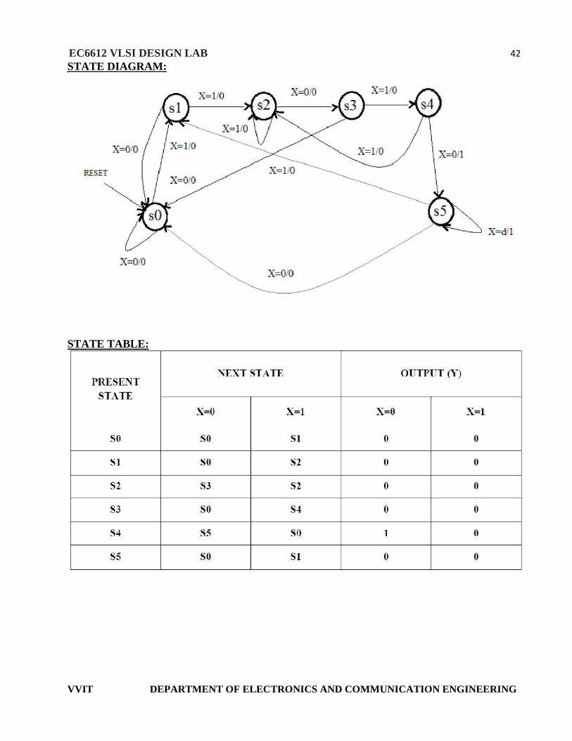
A sequence detector is the one which detects the next state when the reset value is given. The
transition takes place from the present state to the next state when the value is given or else the
present state will be the same state. It can be described using state diagrams. Each state is used to
represent the present state or the next state. The five bit sequence 11010 can be detected using this
state diagram if reset is given then it goes to the next state s1and attains the value 1or else it stays in
the same state s0.
EXP.NO: 10DESIGN OF SEQUENCE DETECTORDATE:

EC6612 VLSI DESIGN LAB 41
VVIT DEPARTMENT OF ELECTRONICS AND COMMUNICATION ENGINEERING
3'b010:beginif (x) beginstate<=3'b010;y<=0;endelse beginstate<=3'b011;y<=0;endend3'b011:beginif (x) beginstate<=3'b100;y<=0;endelse beginstate<=3'b000;y<=0;endend3'b100:beginif (x) beginstate<=3'b000;
y<=0;end
else beginstate<=3'b101;y<=1;endend3'b101:beginif (x) beginstate<=3'b001;y<=0;endelse beginstate<=3'b000;y<=0;endendendcaseendendendmodule
EC6612 VLSI DESIGN LAB 42
VVIT DEPARTMENT OF ELECTRONICS AND COMMUNICATION ENGINEERING
STATE DIAGRAM:
STATE TABLE:

EC6612 VLSI DESIGN LAB 43
VVIT DEPARTMENT OF ELECTRONICS AND COMMUNICATION ENGINEERING
RESULT:
Thus the sequence detector verilog program for to synthesize and simulate using Xilinx
software tool was verified.

EC6612 VLSI DESIGN LAB 44
VVIT DEPARTMENT OF ELECTRONICS AND COMMUNICATION ENGINEERING
TANNERTOOLS
EC6612 VLSI DESIGN LAB 45
VVIT DEPARTMENT OF ELECTRONICS AND COMMUNICATION ENGINEERING
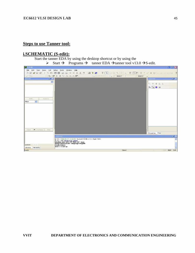
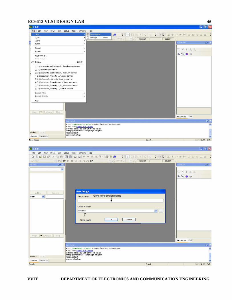
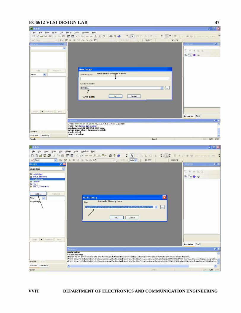
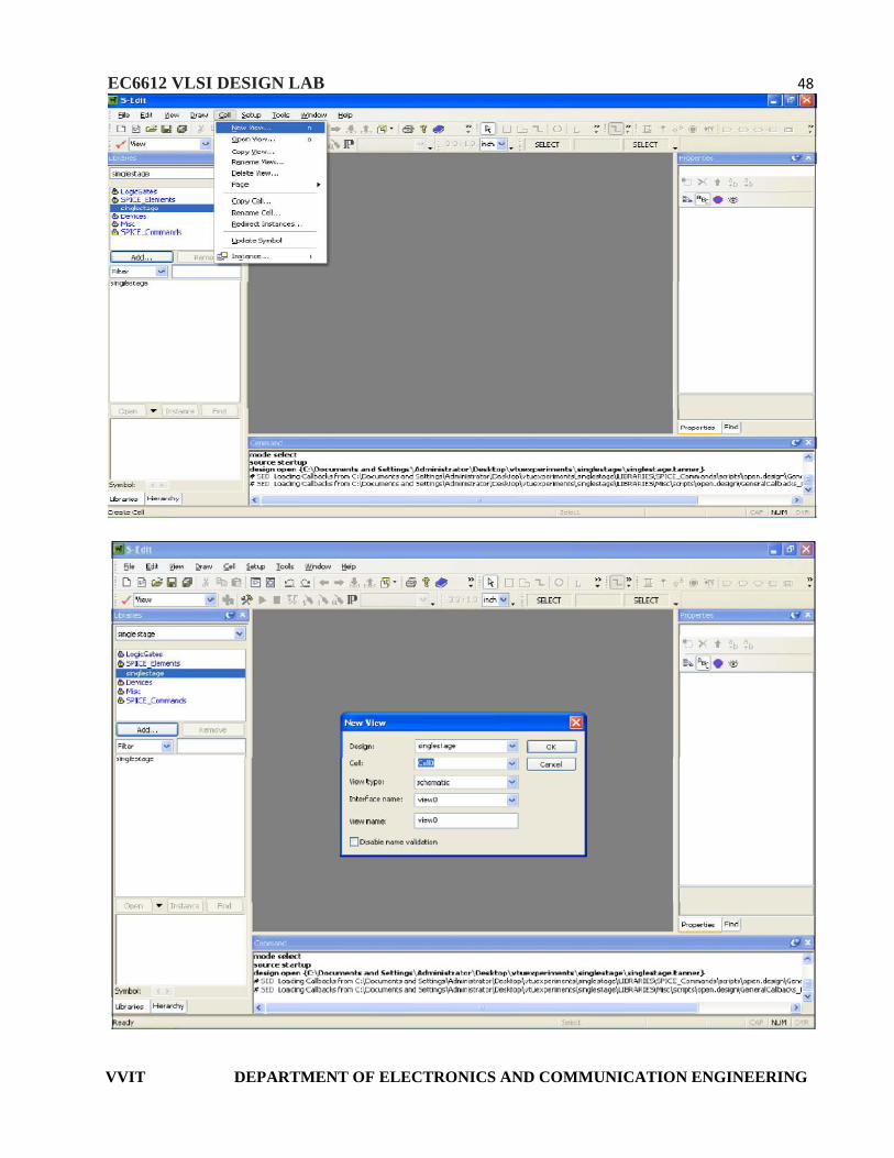
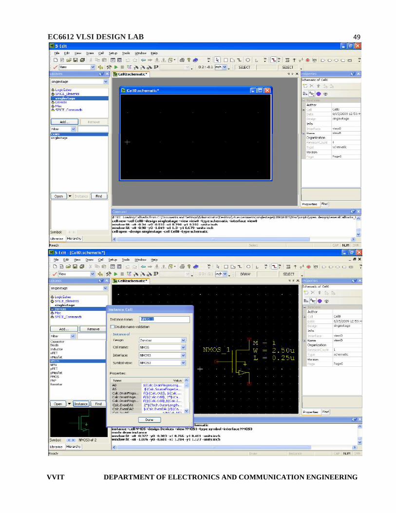
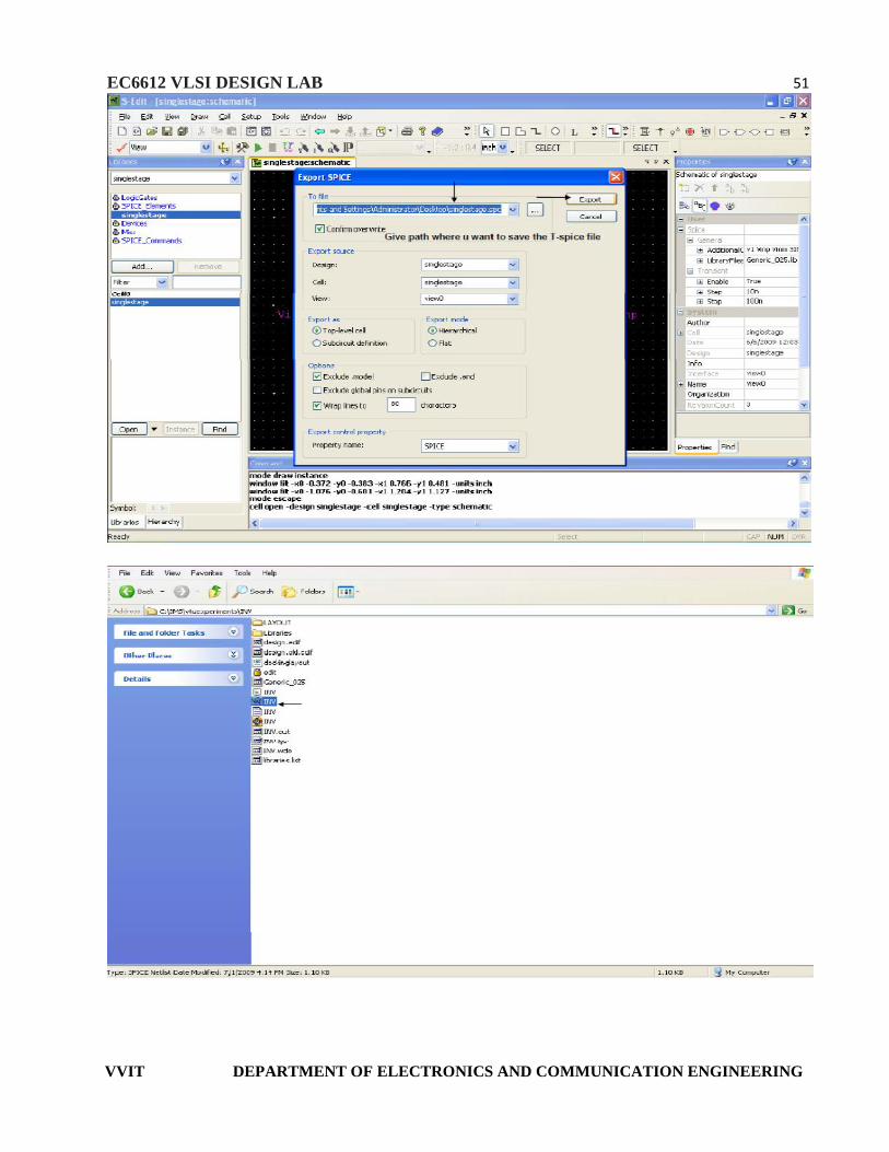
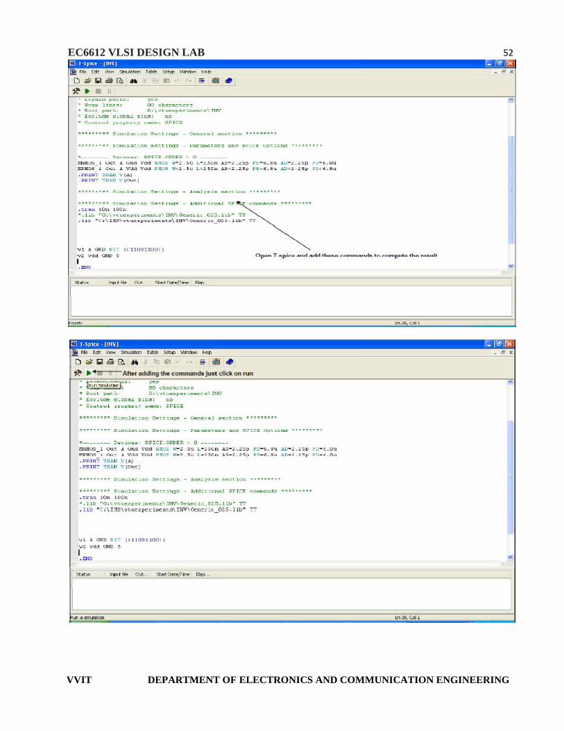
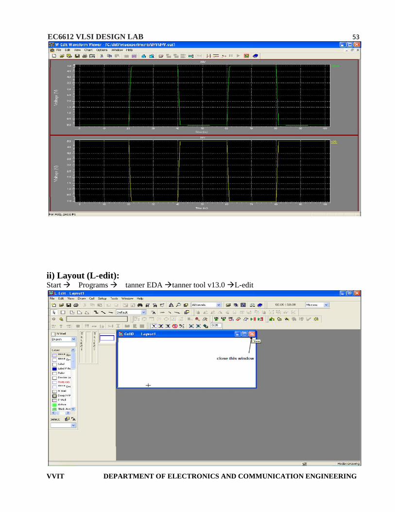
Steps to use Tanner tool:
i.SCHEMATIC (S-edit):Start the tanner EDA by using the desktop shortcut or by using the
StartProgramstanner EDAtanner tool v13.0S-edit.
EC6612 VLSI DESIGN LAB 46
VVIT DEPARTMENT OF ELECTRONICS AND COMMUNICATION ENGINEERING
EC6612 VLSI DESIGN LAB 47
VVIT DEPARTMENT OF ELECTRONICS AND COMMUNICATION ENGINEERING
EC6612 VLSI DESIGN LAB 48
VVIT DEPARTMENT OF ELECTRONICS AND COMMUNICATION ENGINEERING
EC6612 VLSI DESIGN LAB 49
VVIT DEPARTMENT OF ELECTRONICS AND COMMUNICATION ENGINEERING
EC6612 VLSI DESIGN LAB 50
VVIT DEPARTMENT OF ELECTRONICS AND COMMUNICATION ENGINEERING
EC6612 VLSI DESIGN LAB 51
VVIT DEPARTMENT OF ELECTRONICS AND COMMUNICATION ENGINEERING
EC6612 VLSI DESIGN LAB 52
VVIT DEPARTMENT OF ELECTRONICS AND COMMUNICATION ENGINEERING
EC6612 VLSI DESIGN LAB 53
VVIT DEPARTMENT OF ELECTRONICS AND COMMUNICATION ENGINEERING
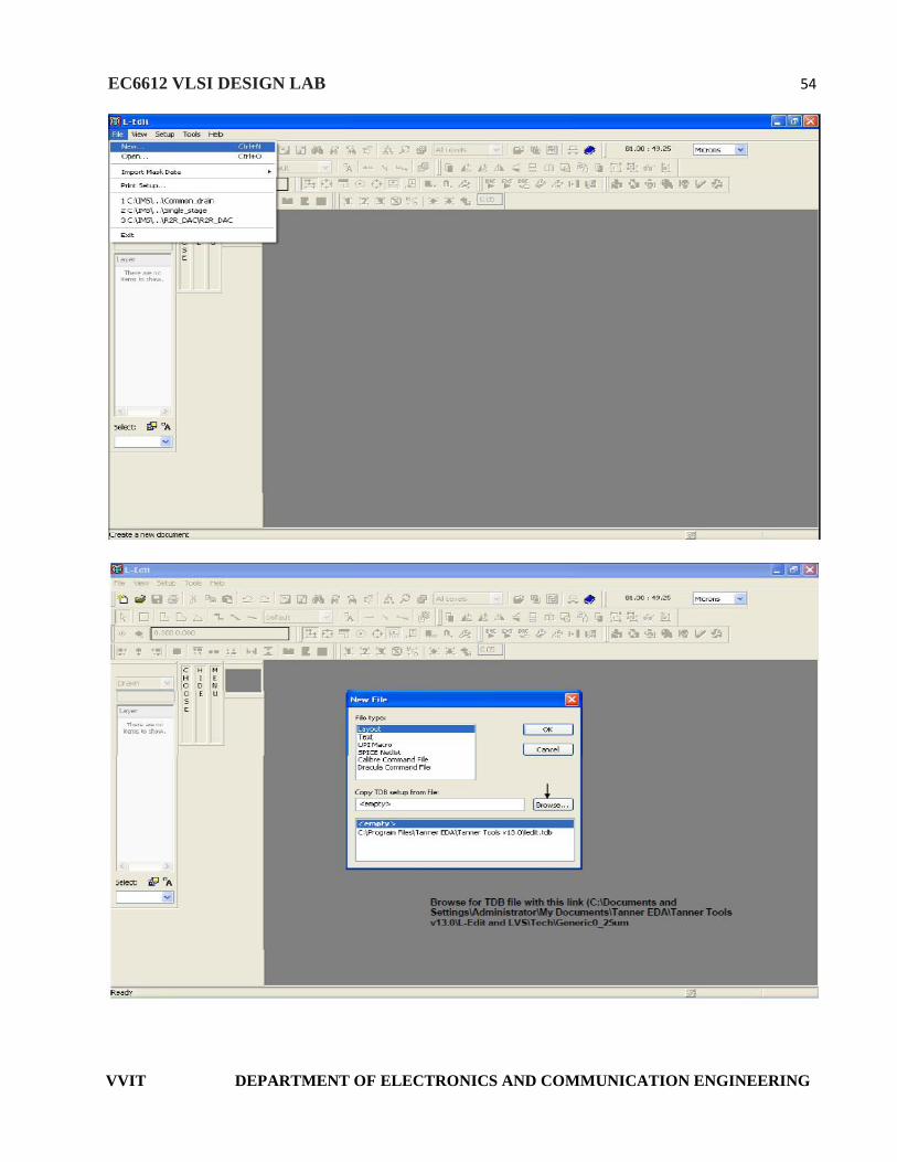
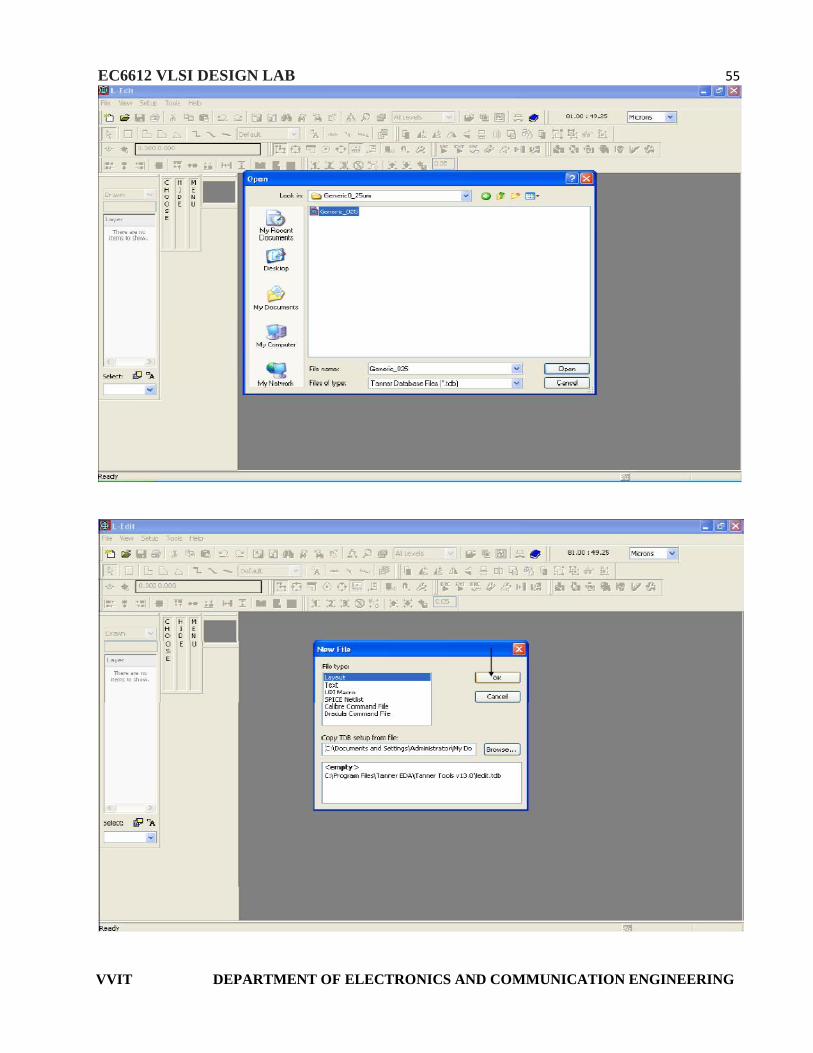
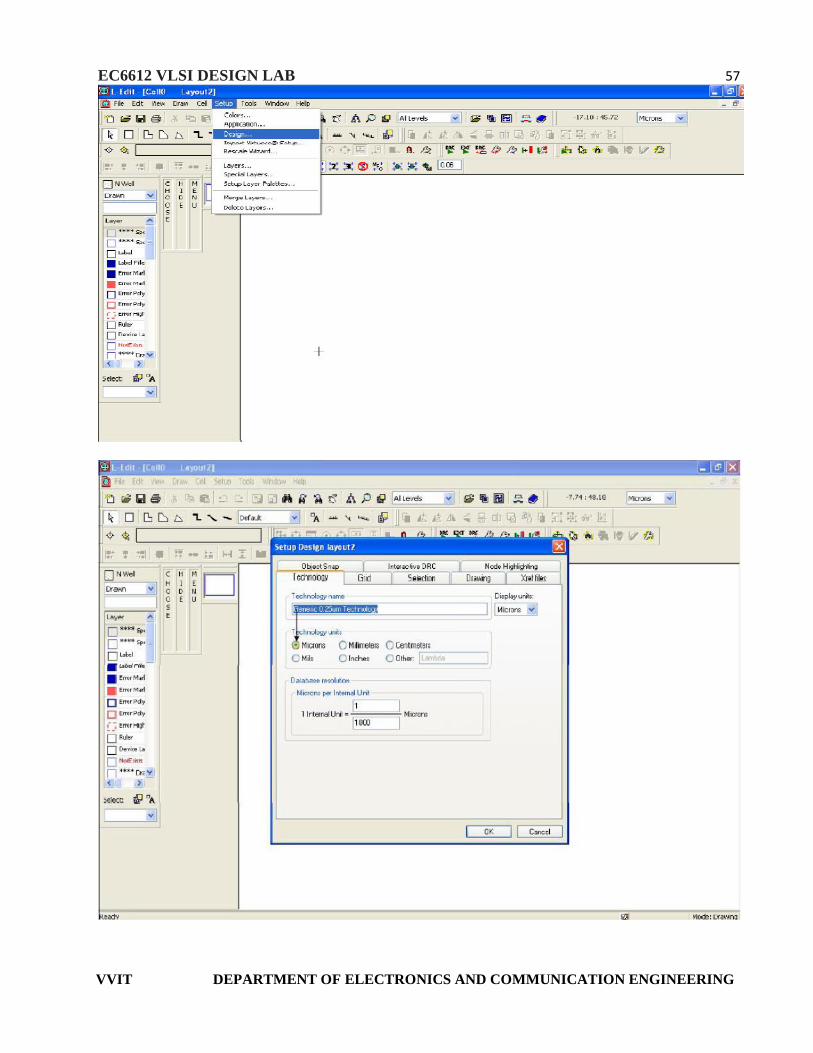
ii) Layout (L-edit):StartProgramstanner EDAtanner tool v13.0L-edit
EC6612 VLSI DESIGN LAB 54
VVIT DEPARTMENT OF ELECTRONICS AND COMMUNICATION ENGINEERING
EC6612 VLSI DESIGN LAB 55
VVIT DEPARTMENT OF ELECTRONICS AND COMMUNICATION ENGINEERING

EC6612 VLSI DESIGN LAB 56
VVIT DEPARTMENT OF ELECTRONICS AND COMMUNICATION ENGINEERING
EC6612 VLSI DESIGN LAB 57
VVIT DEPARTMENT OF ELECTRONICS AND COMMUNICATION ENGINEERING
EC6612 VLSI DESIGN LAB 58
VVIT DEPARTMENT OF ELECTRONICS AND COMMUNICATION ENGINEERING
EC6612 VLSI DESIGN LAB 59
VVIT DEPARTMENT OF ELECTRONICS AND COMMUNICATION ENGINEERING
EC6612 VLSI DESIGN LAB 60
VVIT DEPARTMENT OF ELECTRONICS AND COMMUNICATION ENGINEERING
EC6612 VLSI DESIGN LAB 61
VVIT DEPARTMENT OF ELECTRONICS AND COMMUNICATION ENGINEERING
EC6612 VLSI DESIGN LAB 62
VVIT DEPARTMENT OF ELECTRONICS AND COMMUNICATION ENGINEERING
EC6612 VLSI DESIGN LAB 63
VVIT DEPARTMENT OF ELECTRONICS AND COMMUNICATION ENGINEERING
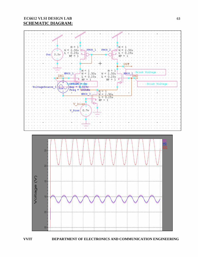
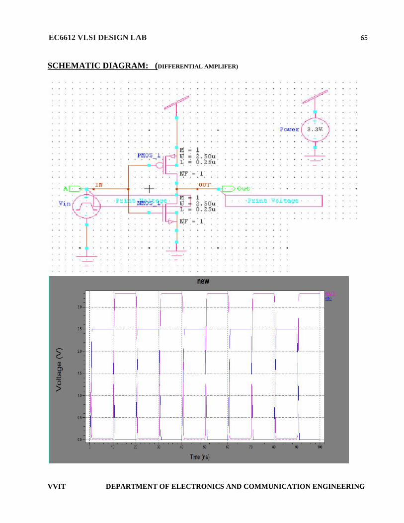
SCHEMATIC DIAGRAM:

EC6612 VLSI DESIGN LAB 64
VVIT DEPARTMENT OF ELECTRONICS AND COMMUNICATION ENGINEERING
AIM:
To calculate the gain, bandwidth and CMRR of a differential amplifier through schematicentry.
FACILITIES REQUIRED:
1. S-Edit using Tanner Tool.
PROCEDURE
1. Draw the schematic of differential amplifier using S-edit and generate the
Symbol.
2. Draw the schematic of differential amplifier circuit using the generated Symbol.
3. Perform AC Analysis of the differential amplifier.
4. Obtain the frequency response from W-edit.
5. Obtain the spice code using T-edit.
RESULT
Thus the differential amplifier bandwidth and CMRR are calculated was verified throughschematic entry.
EXP.NO: 11
DIFFERENTIAL AMPLIFERDATE:
EC6612 VLSI DESIGN LAB 65
VVIT DEPARTMENT OF ELECTRONICS AND COMMUNICATION ENGINEERING
SCHEMATIC DIAGRAM: (DIFFERENTIAL AMPLIFER)

EC6612 VLSI DESIGN LAB 66
VVIT DEPARTMENT OF ELECTRONICS AND COMMUNICATION ENGINEERING
AIM:
To perform the functional verification of the CMOS Inverter through schematic entry.
FACILITIES REQUIRED:
1. S-Edit using Tanner Tool.
PROCEDURE:
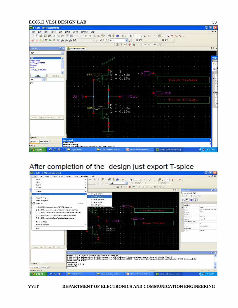
1. Draw the schematic of CMOS Inverter using S-edit
2. Perform Transient Analysis of the CMOS Inverter
3. Obtain the output wave form from W-edit
4. Obtain the spice code using T-edit
THEORY:
Inverter consists of nMOS and pMOS transistor in series connected between VDD and GND.
The gate of the two transistors are shorted and connected to the input. When the input to the inverter
A =0, nMOS transistor is OFF and pMOS transistor is ON. The output is pull-up to VDD.When the
input A=1, nMOS transistor is ON and pMOS transistor is OFF. The Output is Pull-down to GND.
RESULT
Thus the functional verification of the CMOS Inverter was verified through schematic entry.
EXP.NO: 12CMOS INVERTOR
DATE:
EC6612 VLSI DESIGN LAB 67
VVIT DEPARTMENT OF ELECTRONICS AND COMMUNICATION ENGINEERING
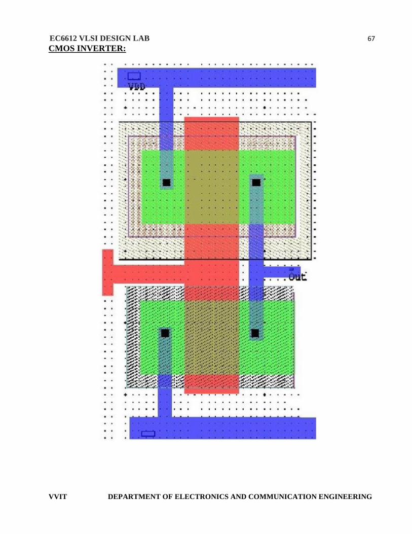
CMOS INVERTER:
EC6612 VLSI DESIGN LAB 68
VVIT DEPARTMENT OF ELECTRONICS AND COMMUNICATION ENGINEERING
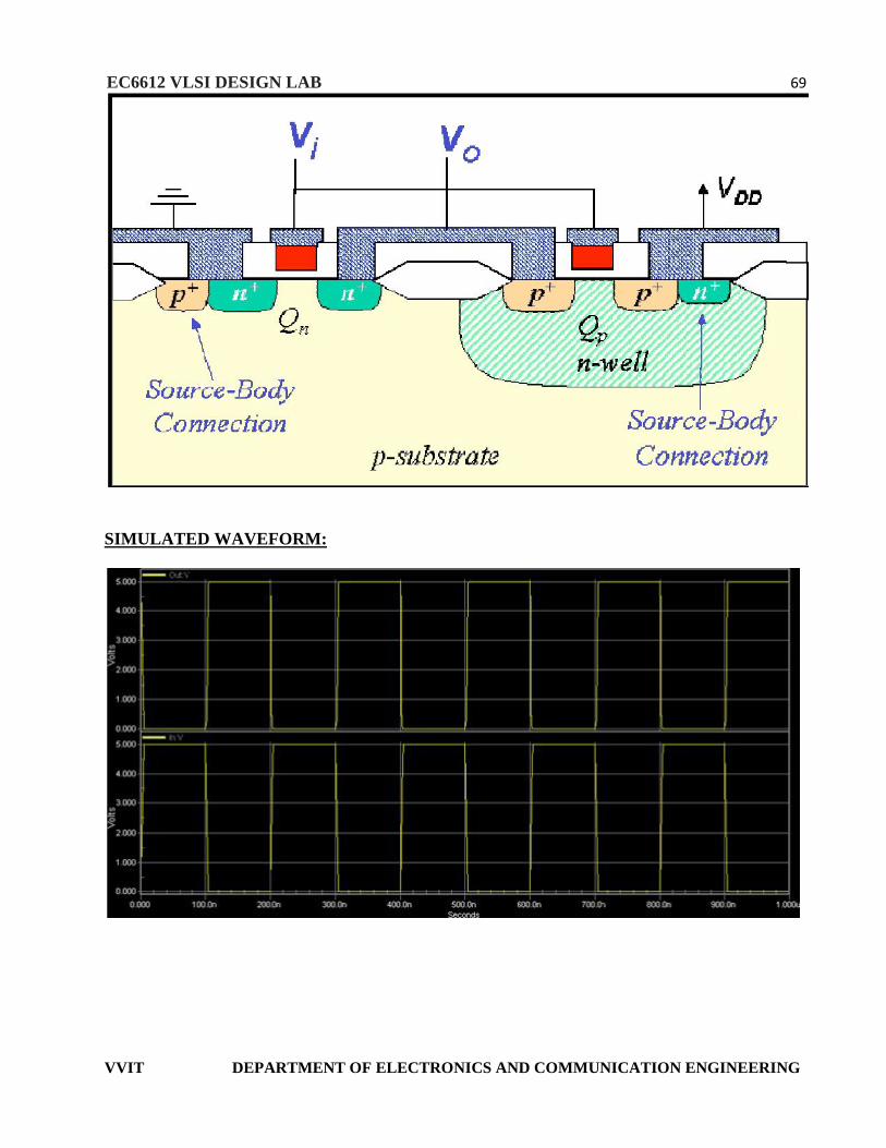
AIM:
To draw the layout of CMOS Inverter using L-Edit and extract the SPICE code.
FACILITIES REQUIRED :
1. L-Edit using Tanner Tool.
PROCEDURE:
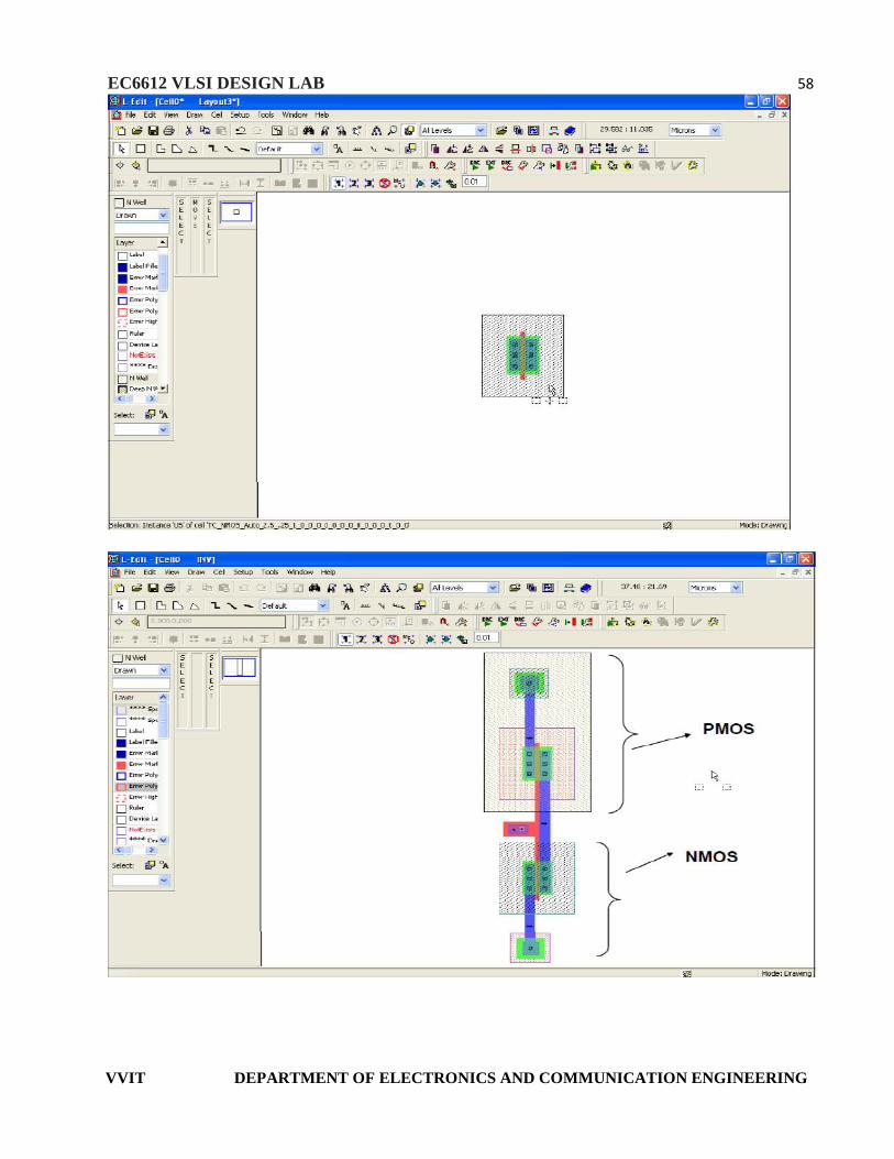
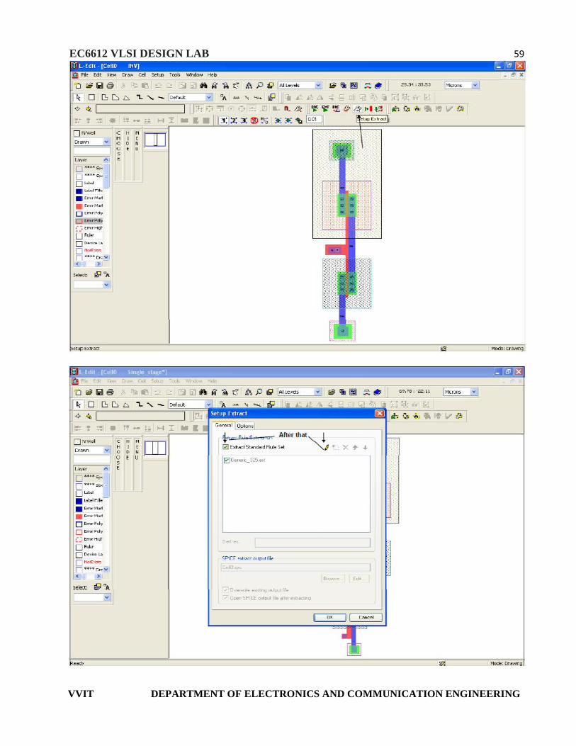
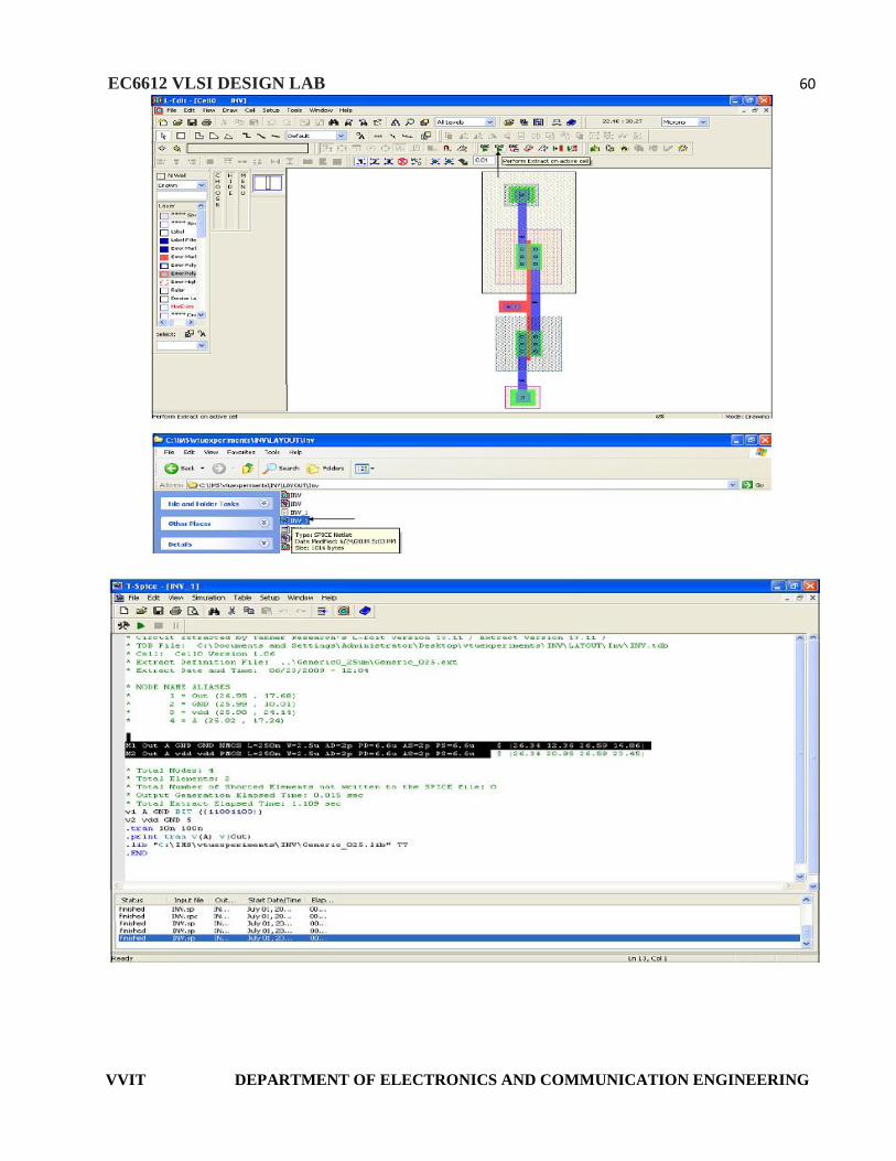
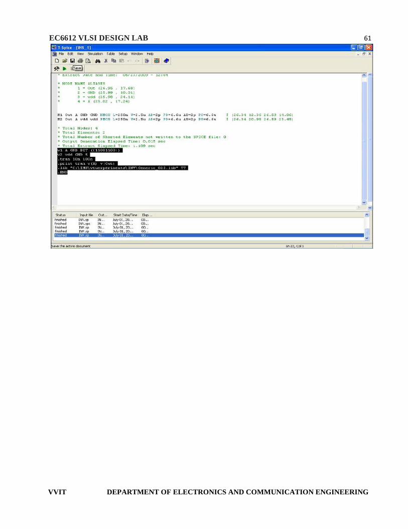
1. Draw the CMOS Inverter layout by obeying the Lamda Rules using L-edit.
2. i. Poly - 2λii.Activecontact -2λ
iii.ActiveContact – Metal -1λiv.ActiveContact – Active region -2λv.ActiveRegion – Pselect -3λ
vi.Pselect – nWell -3λ
3. Check DRC to verify whether any region violate the Lamda rule
4. Setup the extraction and extract the spice code using T-spice.
EXP.NO: 13LAYOUT CMOS INVERTOR
DATE:
EC6612 VLSI DESIGN LAB 69
VVIT DEPARTMENT OF ELECTRONICS AND COMMUNICATION ENGINEERING
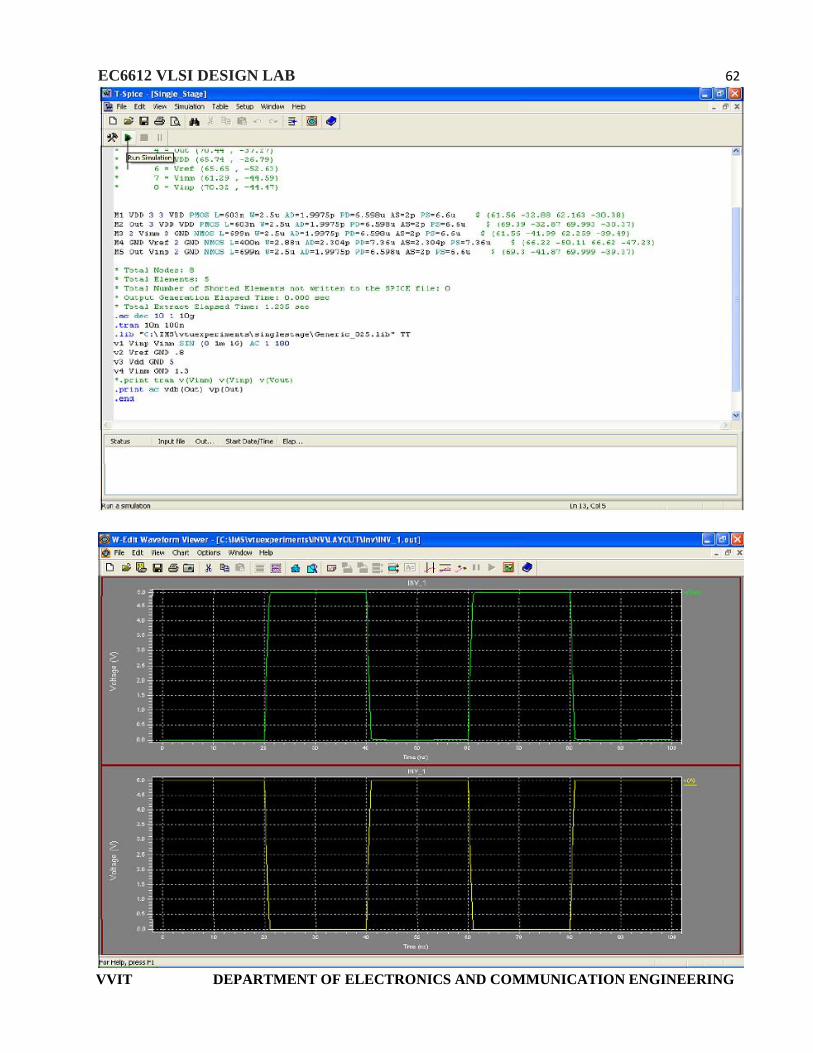
SIMULATED WAVEFORM:

EC6612 VLSI DESIGN LAB 70
VVIT DEPARTMENT OF ELECTRONICS AND COMMUNICATION ENGINEERING
RESULT:
Thus the layout of CMOS Inverter was verified through L-edit.
EC6612 VLSI DESIGN LAB 71
VVIT DEPARTMENT OF ELECTRONICS AND COMMUNICATION ENGINEERING
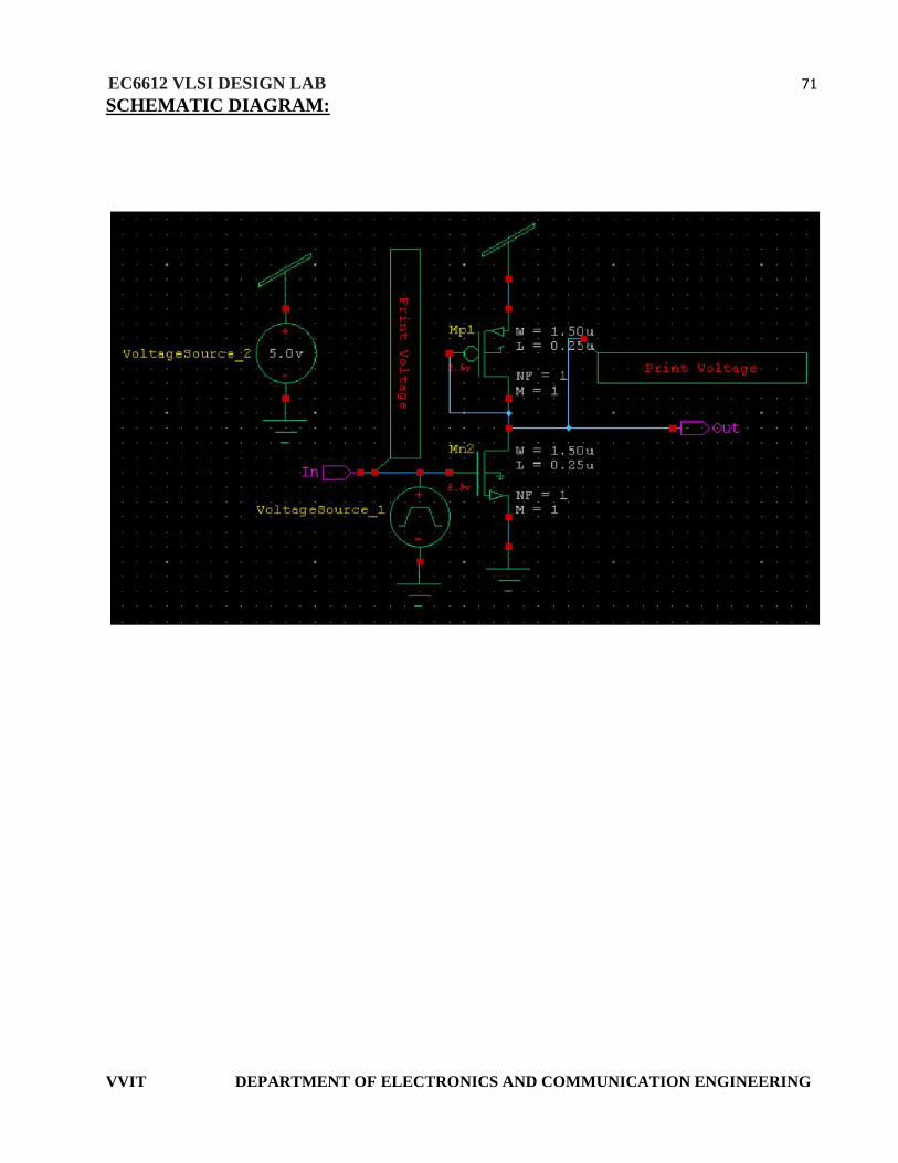
SCHEMATIC DIAGRAM:

EC6612 VLSI DESIGN LAB 72
VVIT DEPARTMENT OF ELECTRONICS AND COMMUNICATION ENGINEERING
AIM:
To generate the automatic Layout from the schematic using the Tanner tool and verify
the layout using simulation.
FACILITIES REQUIRED
1. S-Edit and L-Edit using Tanner Tool
PROCEDURE
1. Draw the schematic using S -Edit and verify the output in W-Edit.
2. Extract the schematic and store it in another location
3. Open the L-Edit, open the design in Ring VCO
4. Create the new cell
5. Open the schematic file(.sdl) using the SDL Navigator
6. Do the necessary connections as per the design.
7. Name the ports and check the design for the DRC Rules
8. Locate the Destination file in the setup Extract window and extract the layout.
9. Include the Library and the print voltage statements in the net list which is
obtained.
10. Verify the layout design using W-Edit.
EXP.NO: 14AUTOMATIC LAYOUT GENERATION
DATE:
EC6612 VLSI DESIGN LAB 73
VVIT DEPARTMENT OF ELECTRONICS AND COMMUNICATION ENGINEERING
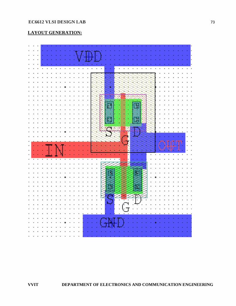
LAYOUT GENERATION:
EC6612 VLSI DESIGN LAB 74
VVIT DEPARTMENT OF ELECTRONICS AND COMMUNICATION ENGINEERING
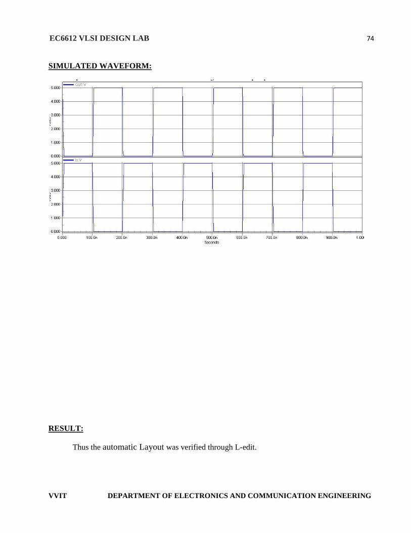
SIMULATED WAVEFORM:
RESULT:
Thus the automatic Layout was verified through L-edit.