IC DESIGN, Presented by MURALI.A. AGENDA OVERVIEW OF ELECTRONIC DESIGN VLSI DESIGN FLOW – FRONT...
38
IC DESIGN Presented by MURALI.A
-
Upload
rudolph-george -
Category
Documents
-
view
231 -
download
1
Transcript of IC DESIGN, Presented by MURALI.A. AGENDA OVERVIEW OF ELECTRONIC DESIGN VLSI DESIGN FLOW – FRONT...
IC DESIGN,
,
Presented by MURALI.A
AGENDA
• OVERVIEW OF ELECTRONIC DESIGN• VLSI DESIGN FLOW
– FRONT END DESIGN– BACK END DESIGN
• FPGA-FLOW• FPGA vs ASIC
MURALI.A, FACULTY DEPT OF ECE, LIET HYDERABAD
Common Products• Communication
• Mobiles / Telephones / RF / Satellite
• Video Audio • TV / Audio players / Video players
• Computers • PC / Laptop / PDAs / Memory
• Networking • Switches / Routers / Wi-Fi
• Print • Printers / Fax / Scanners
• Cameras • Video camera / Still cameras
• Video Gaming • Xbox / PlayStation
MURALI.A, FACULTY DEPT OF ECE, LIET HYDERABAD
• Consumer
• Automobile» Sensors / Control
• Defense» Military / Air Force / Navel
• Space & Avionics» Satellites / Airlines/ GPS
• Industrial » Automation
Industries
MURALI.A, FACULTY DEPT OF ECE, LIET HYDERABAD

Product Development
Chip Design
Hardware Integration
Low Level Software
Application software
Generic ICs like Microprocessors & RAMsApplication Specific ICs (ASICs)
Programmable Chips (FPGA/EPLD)
Board DesignPower supply
Integration
Operating SystemsDevice Drivers, Memory Managers
Multi Threading
Applications/Solutions/User-Interface
MURALI.A, FACULTY DEPT OF ECE, LIET HYDERABAD
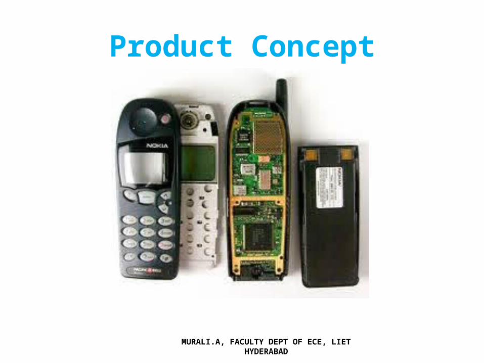
Product Concept
MURALI.A, FACULTY DEPT OF ECE, LIET HYDERABAD
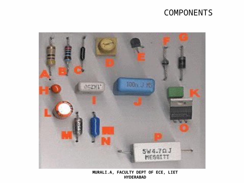
COMPONENTS
MURALI.A, FACULTY DEPT OF ECE, LIET HYDERABAD
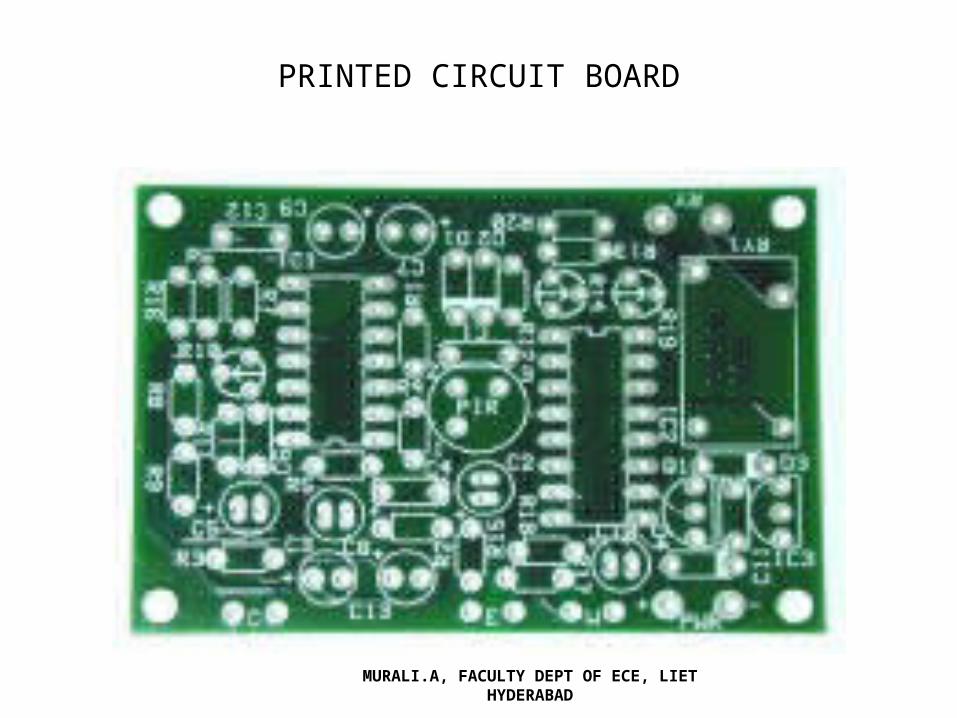
PRINTED CIRCUIT BOARD
MURALI.A, FACULTY DEPT OF ECE, LIET HYDERABAD

Hardware
MURALI.A, FACULTY DEPT OF ECE, LIET HYDERABAD
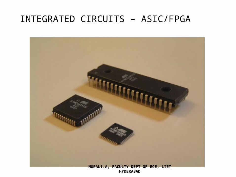
INTEGRATED CIRCUITS – ASIC/FPGA
MURALI.A, FACULTY DEPT OF ECE, LIET HYDERABAD

Fab
PCB ASIC
Hardware Development
Electronics
Front End
VerificationDesign
Back EndMakeDesign Layout
MURALI.A, FACULTY DEPT OF ECE, LIET HYDERABAD
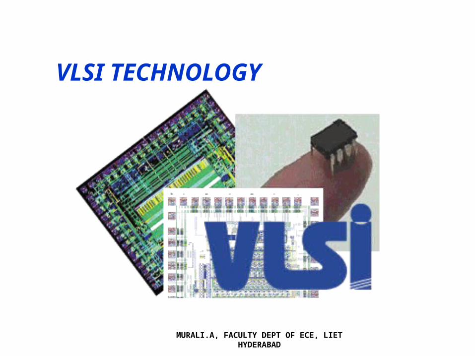
VLSI TECHNOLOGY
MURALI.A, FACULTY DEPT OF ECE, LIET HYDERABAD
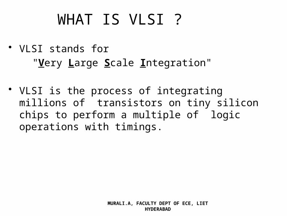
WHAT IS VLSI ?
• VLSI stands for "Very Large Scale Integration"
• VLSI is the process of integrating millions of transistors on tiny silicon chips to perform a multiple of logic operations with timings.
MURALI.A, FACULTY DEPT OF ECE, LIET HYDERABAD
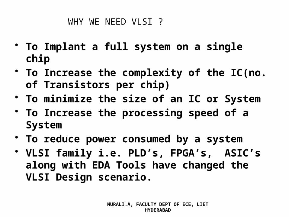
WHY WE NEED VLSI ?
• To Implant a full system on a single chip• To Increase the complexity of the IC(no. of Transistors per
chip)• To minimize the size of an IC or System• To Increase the processing speed of a System• To reduce power consumed by a system• VLSI family i.e. PLD’s, FPGA’s, ASIC’s along with EDA Tools
have changed the VLSI Design scenario.
MURALI.A, FACULTY DEPT OF ECE, LIET HYDERABAD
Scope of VLSI Engineers
Design engineer. Product engineer. Test engineer. Application engineer. Process engineer. Packaging engineer. CAD engineer.
MURALI.A, FACULTY DEPT OF ECE, LIET HYDERABAD
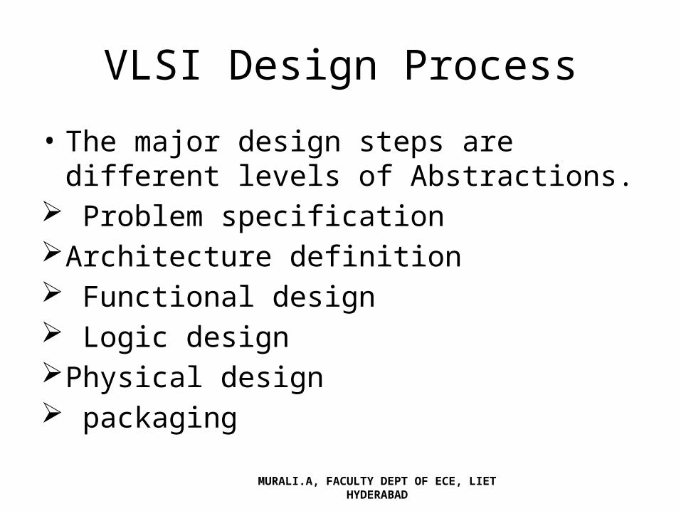
VLSI Design Process
• The major design steps are different levels of Abstractions.
Problem specificationArchitecture definition Functional design Logic designPhysical design packaging
MURALI.A, FACULTY DEPT OF ECE, LIET HYDERABAD
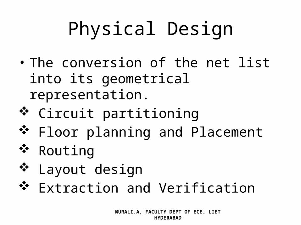
Physical Design
• The conversion of the net list into its geometrical representation.
Circuit partitioning Floor planning and Placement Routing Layout design Extraction and Verification
MURALI.A, FACULTY DEPT OF ECE, LIET HYDERABAD

What jobs does an VLSI Engineers do?
Design engineer. Product engineer. Test engineer. Application engineer. Process engineer. Packaging engineer. CAD engineer.
MURALI.A, FACULTY DEPT OF ECE, LIET HYDERABAD
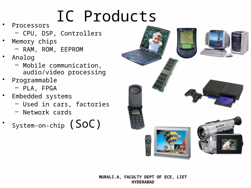
IC Products• Processors
– CPU, DSP, Controllers• Memory chips
– RAM, ROM, EEPROM• Analog
– Mobile communication,audio/video processing
• Programmable– PLA, FPGA
• Embedded systems– Used in cars, factories– Network cards
• System-on-chip (SoC)
MURALI.A, FACULTY DEPT OF ECE, LIET HYDERABAD
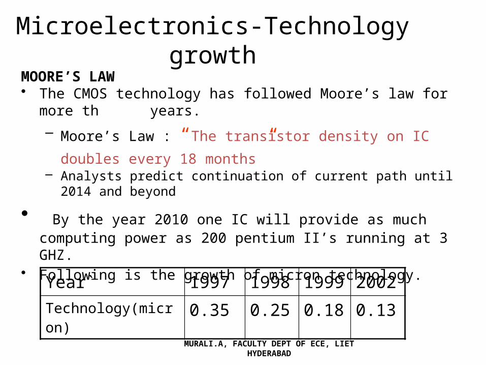
Microelectronics-Technology growthMOORE’S LAW• The CMOS technology has followed Moore’s law for more than 20 years.
– Moore’s Law : “The transistor density on IC doubles every 18
months”– Analysts predict continuation of current path until 2014 and beyond
• By the year 2010 one IC will provide as much computing power as 200 pentium II’s running at 3 GHZ.
• Following is the growth of micron technology.
Year` 1997 1998 1999 2002
Technology(micron) 0.35 0.25 0.18 0.13
MURALI.A, FACULTY DEPT OF ECE, LIET HYDERABAD
MURALI.A, FACULTY DEPT OF ECE, LIET HYDERABAD
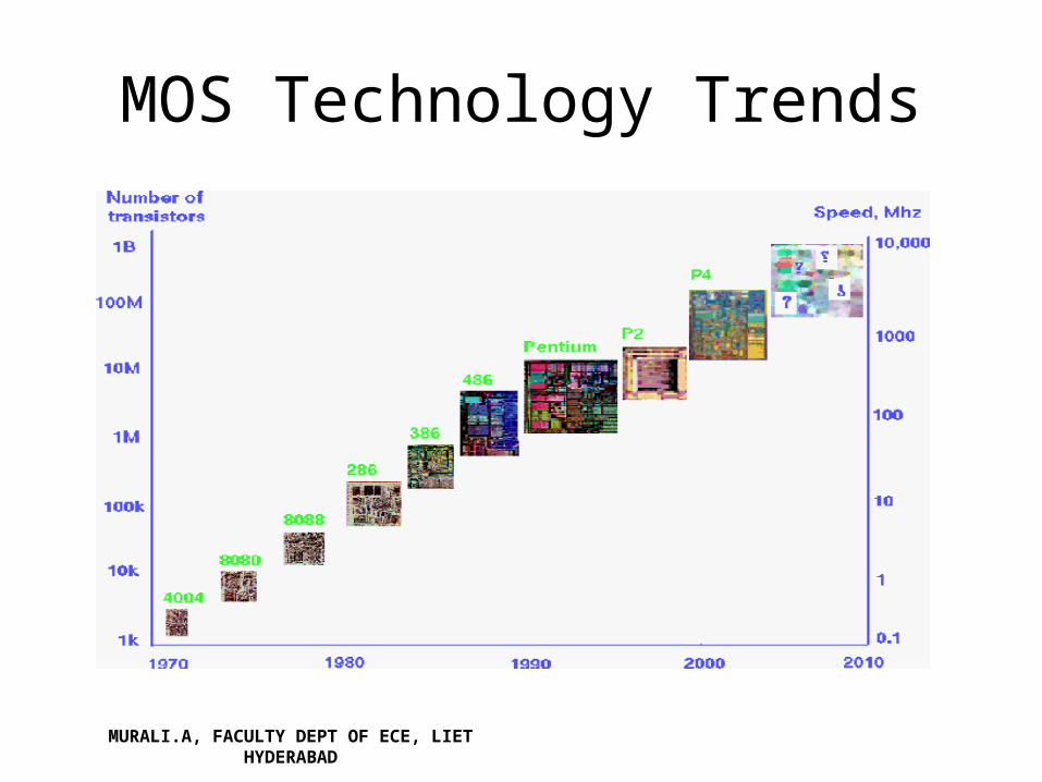
MOS Technology Trends

Integrated Circuits
SSI / MSIA few thousand transistors 1960s
LSIProcessors, 1Kb Memory 1970s
VLSIMillions of transistors
Growth of EDA/ComputingVHDL/Verilog
1980s
ULSIBillions of transistorsMulti Core processors
64-bit processorsSystem-On-Chip DRAMs / Flash
90nm / 60nm / 28nm
21st Century
Process ImprovementsCost/Speed/Low-Power
180nm / 130nm1990s
Programmable ChipsFPGA/EPLD/CPLD
SOPCsMulti million gate
High Speed
FPGAsApplication Specific Designs
High Performance Computing
New ApplicationsMobile / Consumer / Industrial
EntertainmentVideo / Gaming / Graphics
Smart Phones

INTEL-PROCESSORS– An Evolution..
MURALI.A, FACULTY DEPT OF ECE, LIET HYDERABAD
VLSI DESIGN FLOW
MURALI.A, FACULTY DEPT OF ECE, LIET HYDERABAD

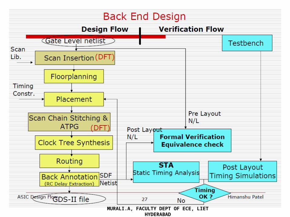
Specifications
Design Verification
Verilog/VHDL Simulation Models
Synthesis Functional Simulation
Pre Route STA
Clock Tree Synthesis
Placement
Routing
Netlist - SDF
Libs / Const
Post Route STA
Libs / Const
Gate Level Simulations
ModelsimVCS
NCSim
VerilogVHDLC/Perl
SysVerilogSpecman
Formal Verification
MURALI.A, FACULTY DEPT OF ECE, LIET HYDERABAD
text
texttext
MURALI.A, FACULTY DEPT OF ECE, LIET HYDERABAD
MURALI.A, FACULTY DEPT OF ECE, LIET HYDERABAD
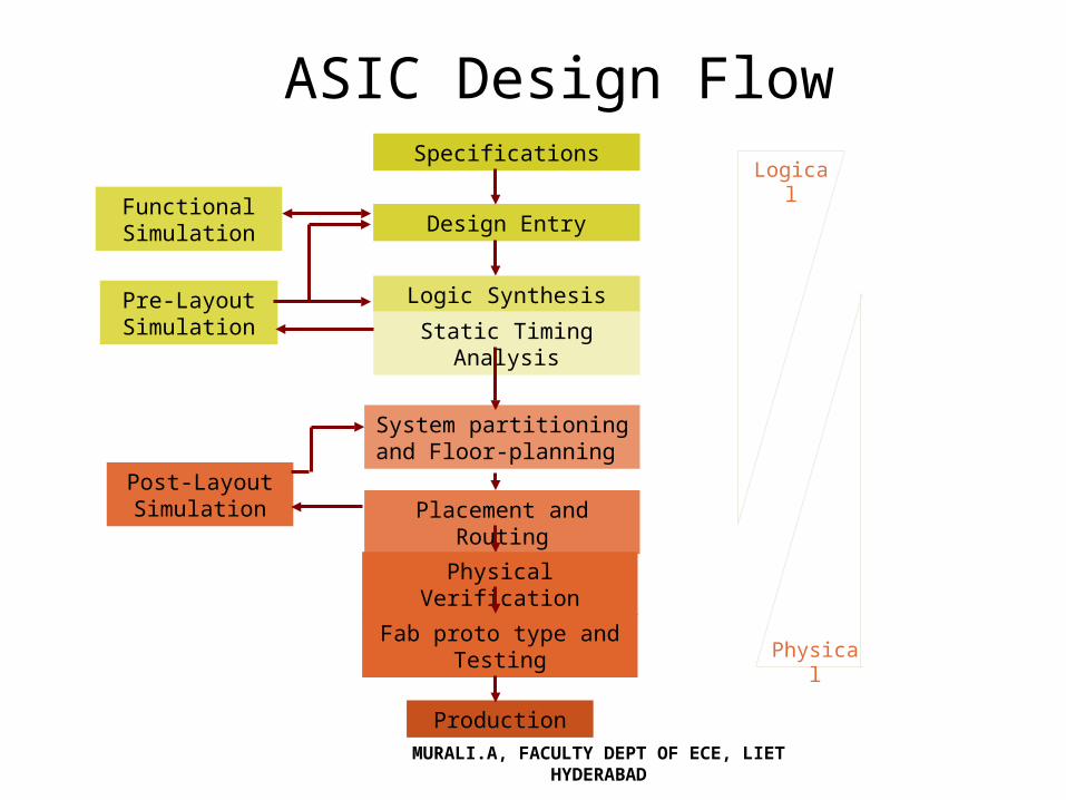
ASIC Design FlowSpecifications
Functional Simulation
Logic Synthesis
Design Entry
Static Timing Analysis
System partitioning and Floor-planning
Placement and RoutingPost-Layout Simulation
Fab proto type and Testing
Production
Pre-Layout Simulation
Logical
Physical
Physical Verification

MURALI.A, FACULTY DEPT OF ECE, LIET HYDERABAD
MURALI.A, FACULTY DEPT OF ECE, LIET HYDERABAD

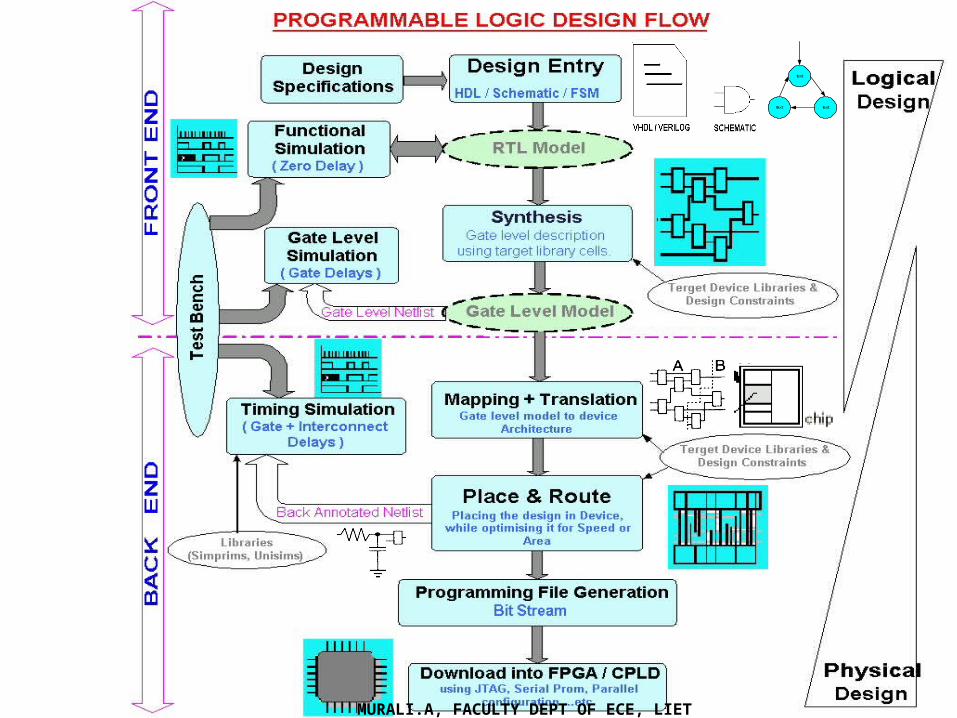
FPGA Design Flow
Schematics HDL
Design entry
synthesis
mapping
Place & route
Configuration
simulation
MURALI.A, FACULTY DEPT OF ECE, LIET HYDERABAD
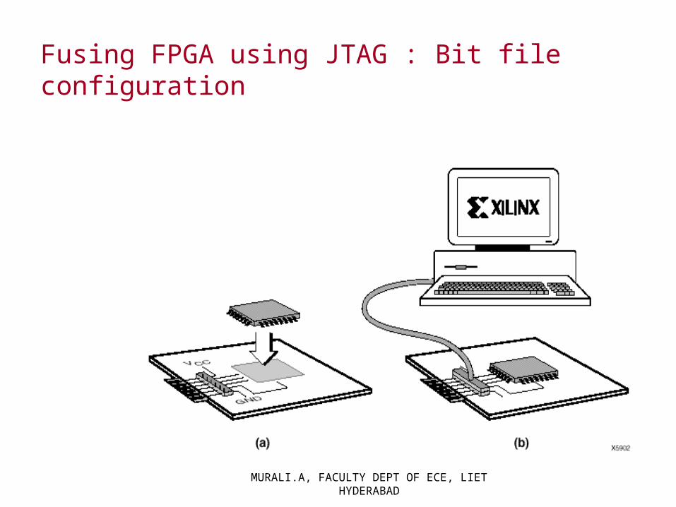
Fusing FPGA using JTAG : Bit file configuration
MURALI.A, FACULTY DEPT OF ECE, LIET HYDERABAD
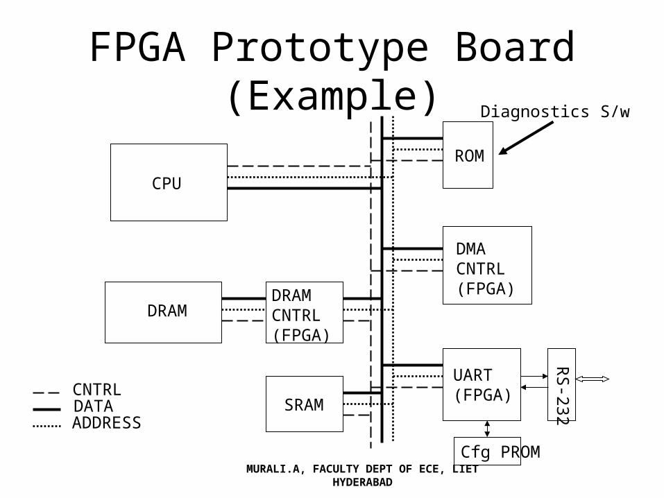
FPGA Prototype Board (Example)
CPU
DRAMDRAMCNTRL(FPGA)
SRAM
ROM
DMACNTRL(FPGA)
UART(FPGA)
RS-232CNTRLDATAADDRESS
Cfg PROM
Diagnostics S/w
MURALI.A, FACULTY DEPT OF ECE, LIET HYDERABAD

FPGA’s on PCB’s
MURALI.A, FACULTY DEPT OF ECE, LIET HYDERABAD

Suppliers of Programmable Logic Devices
Xilinx Altera Cypress Lattice Philips Vantis Cirrus Logic Quick Logic Actel Atmel Lucent
MURALI.A, FACULTY DEPT OF ECE, LIET HYDERABAD
Different kinds of programmable logic devices available today
• Major types :
i. Simple Programmable Logic Devices (SPLDs) ii. Complex Programmable Logic Devices (CPLDs) iii. Field Programmable Gate Arrays (FPGAs)
MURALI.A, FACULTY DEPT OF ECE, LIET HYDERABAD
SPLDs & CPLDs• SPLDs are also known as:
– PAL (Programmable Array Logic, Vantis) – GAL (Generic Array Logic, Lattice) – PLA (Programmable Logic Array) – PLD (Programmable Logic Device)
• SPLDs are the smallest and consequently the least-expensive form of programmable logic.It Contains 4 to 22 macrocells and can typically replace a few 7400-series TTL devices
• Array of SPLDs can say as CPLDs
MURALI.A, FACULTY DEPT OF ECE, LIET HYDERABAD
MURALI.A, FACULTY DEPT OF ECE, LIET HYDERABAD
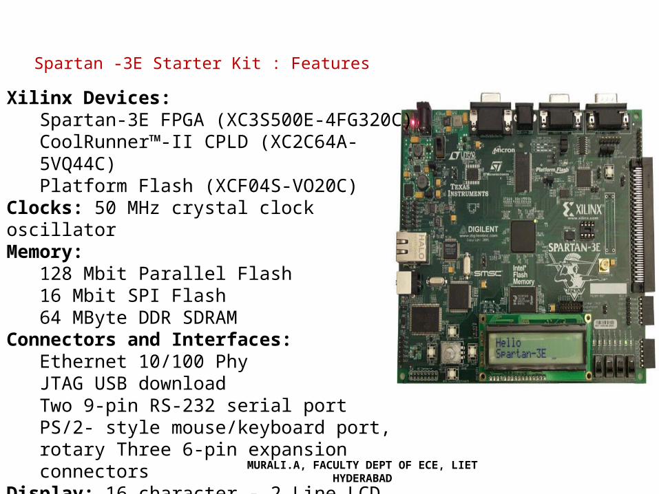
Spartan -3E Starter Kit : Features
Xilinx Devices: Spartan-3E FPGA (XC3S500E-4FG320C)CoolRunner™-II CPLD (XC2C64A-5VQ44C)Platform Flash (XCF04S-VO20C)
Clocks: 50 MHz crystal clock oscillatorMemory:
128 Mbit Parallel Flash16 Mbit SPI Flash64 MByte DDR SDRAM
Connectors and Interfaces: Ethernet 10/100 PhyJTAG USB downloadTwo 9-pin RS-232 serial portPS/2- style mouse/keyboard port, rotary Three 6-pin expansion connectors
Display: 16 character - 2 Line LCD
Thank - U
MURALI.A, FACULTY DEPT OF ECE, LIET HYDERABAD