ECE 448 – FPGA and ASIC Design with VHDL Lecture 12 PicoBlaze Overview.
Upload
nguyenquynhCategory
view
273download
2
George Mason University ECE 448 – FPGA and ASIC Design with VHDL
FPGA Devices & FPGA Design Flow
ECE 448 Lecture 5

2
Required reading
• Spartan-6 FPGA Configurable Logic Block: User Guide
§ CLB Overview § Slice Description

3 ECE 448 – FPGA and ASIC Design with VHDL
Block R
AM
s
Block R
AM
s
Configurable Logic Blocks
I/O Blocks
What is an FPGA?
Block RAMs

4
Modern FPGA RAM blocks
Multipliers
Logic blocks
Graphics based on The Design Warrior’s Guide to FPGAs Devices, Tools, and Flows. ISBN 0750676043
Copyright © 2004 Mentor Graphics Corp. (www.mentor.com)
Multipliers/DSP units
RAM blocks
Logic resources
(#Logic resources, #Multipliers/DSP units, #RAM_blocks)

5 ECE 448 – FPGA and ASIC Design with VHDL
Major FPGA Vendors SRAM-based FPGAs • Xilinx, Inc. • Altera Corp. • Lattice Semiconductor • Atmel • Achronix • Tabula Flash & antifuse FPGAs • Microsemi SoC Products Group (formerly Actel Corp.) • Quick Logic Corp.
~ 51% of the market
~ 34% of the market ~ 85%

6 ECE 448 – FPGA and ASIC Design with VHDL
Xilinx u Primary products: FPGAs and the associated CAD
software
u Main headquarters in San Jose, CA u Fabless* Semiconductor and Software Company
u UMC (Taiwan) {*Xilinx acquired an equity stake in UMC in 1996} u Seiko Epson (Japan) u TSMC (Taiwan) u Samsung (Korea)
Programmable Logic Devices ISE Alliance and Foundation
Series Design Software

Technology Low-‐cost High-‐performance
220 nm Virtex 180 nm Spartan-‐II,
Spartan-‐IIE 120/150 nm Virtex-‐II,
Virtex-‐II Pro 90 nm Spartan-‐3 Virtex-‐4 65 nm Virtex-‐5 45 nm Spartan-‐6 40 nm Virtex-‐6 28 nm Ar>x-‐7 Virtex-‐7
Xilinx FPGA Families

8
FPGA Family

9 ECE 448 – FPGA and ASIC Design with VHDL
Spartan-6 FPGA Family
George Mason University ECE 448 – FPGA and ASIC Design with VHDL
CLB Structure
11 ECE 448 – FPGA and ASIC Design with VHDL
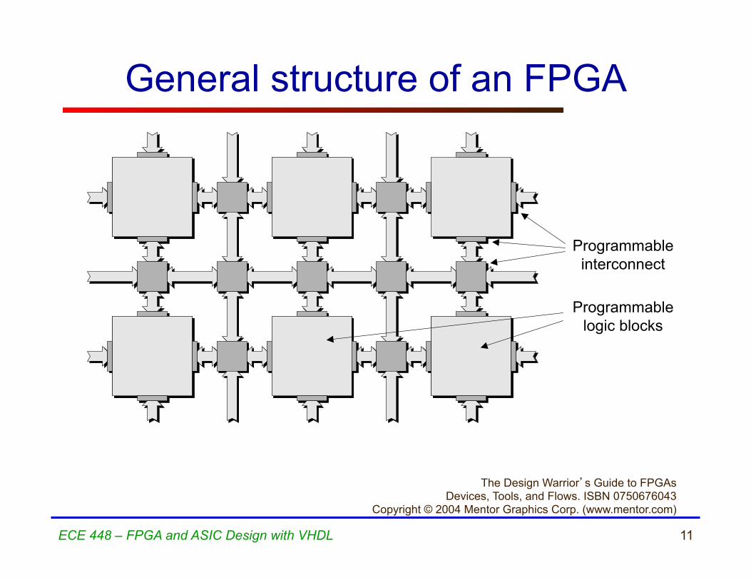
Programmableinterconnect
Programmablelogic blocks
The Design Warrior’s Guide to FPGAs Devices, Tools, and Flows. ISBN 0750676043
Copyright © 2004 Mentor Graphics Corp. (www.mentor.com)
General structure of an FPGA

12 ECE 448 – FPGA and ASIC Design with VHDL
Xilinx Spartan-6 CLB

13 ECE 448 – FPGA and ASIC Design with VHDL
Row & Column Relationship Between CLBs & Slices

14 ECE 448 – FPGA and ASIC Design with VHDL
SLICEX

15 ECE 448 – FPGA and ASIC Design with VHDL
4-input LUT (Look-Up Table) (used in earlier families of FPGAs)
• Look-Up tables are primary elements for logic implementation
• Each LUT can implement any function of 4 inputs
x1 x2 x3 x4
y
x1 x2
y
LUT
x1x2x3x4
y
0x1
0x2 x3 x4
0 00 0 0 10 0 1 00 0 1 10 1 0 00 1 0 10 1 1 00 1 1 11 0 0 01 0 0 11 0 1 01 0 1 11 1 0 01 1 0 11 1 1 01 1 1 1
y0100010101001100
0x1
0x2 x3 x4
0 00 0 0 10 0 1 00 0 1 10 1 0 00 1 0 10 1 1 00 1 1 11 0 0 01 0 0 11 0 1 01 0 1 11 1 0 01 1 0 11 1 1 01 1 1 1
y1111111111110000
x1 x2 x3 x4
y
x1 x2 x3 x4
y
x1 x2
y
x1 x2
y
LUT
x1x2x3x4
y
0x1
0x2 x3 x4
0 00 0 0 10 0 1 00 0 1 10 1 0 00 1 0 10 1 1 00 1 1 11 0 0 01 0 0 11 0 1 01 0 1 11 1 0 01 1 0 11 1 1 01 1 1 1
y0100010101001100
0x1
0x2 x3 x4
0 00 0 0 10 0 1 00 0 1 10 1 0 00 1 0 10 1 1 00 1 1 11 0 0 01 0 0 11 0 1 01 0 1 11 1 0 01 1 0 11 1 1 01 1 1 1
y0100010101001100
0x1
0x2 x3 x4
0 00 0 0 10 0 1 00 0 1 10 1 0 00 1 0 10 1 1 00 1 1 11 0 0 01 0 0 11 0 1 01 0 1 11 1 0 01 1 0 11 1 1 01 1 1 1
y1111111111110000
0x1
0x2 x3 x4
0 00 0 0 10 0 1 00 0 1 10 1 0 00 1 0 10 1 1 00 1 1 11 0 0 01 0 0 11 0 1 01 0 1 11 1 0 01 1 0 11 1 1 01 1 1 1
y1111111111110000

16 ECE 448 – FPGA and ASIC Design with VHDL
6-Input LUT of Spartan-6
17

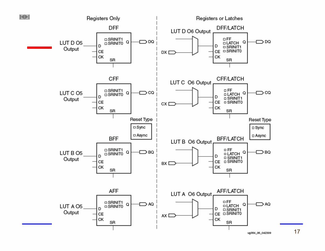
18 ECE 448 – FPGA and ASIC Design with VHDL
Reset and Set Configurations
• No set or reset • Synchronous set • Synchronous reset • Asynchronous set (preset) • Asynchronous reset (clear)

19 ECE 448 – FPGA and ASIC Design with VHDL
Three Different Types of Slices
50% 25% 25%

20
SLICEL

21
u Each CLB contains separate logic and routing for the fast generation of sum & carry signals • Increases efficiency and
performance of adders, subtractors, accumulators, comparators, and counters
u Carry logic is independent of normal logic and routing resources
Fast Carry Logic
LSB
MSB
Carry
Log
ic Ro
utin
g
22
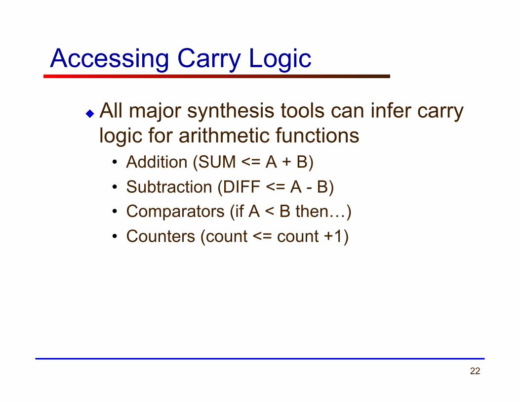
Accessing Carry Logic
u All major synthesis tools can infer carry logic for arithmetic functions
• Addition (SUM <= A + B) • Subtraction (DIFF <= A - B) • Comparators (if A < B then…) • Counters (count <= count +1)

23 ECE 448 – FPGA and ASIC Design with VHDL
SLICEM

24
16-bit SR
16 x 1 RAM
4-input LUT
The Design Warrior’s Guide to FPGAs Devices, Tools, and Flows. ISBN 0750676043
Copyright © 2004 Mentor Graphics Corp. (www.mentor.com)
Xilinx Multipurpose LUT (MLUT)
64 x 1 ROM (logic)
64 x 1 RAM
32-bit SR

25
Single-port 64 x 1-bit RAM
26
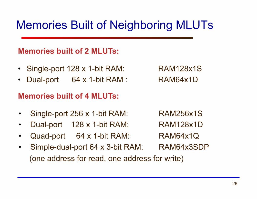
Memories Built of Neighboring MLUTs
• Single-port 128 x 1-bit RAM: RAM128x1S • Dual-port 64 x 1-bit RAM : RAM64x1D
Memories built of 2 MLUTs:
Memories built of 4 MLUTs:
• Single-port 256 x 1-bit RAM: RAM256x1S • Dual-port 128 x 1-bit RAM: RAM128x1D • Quad-port 64 x 1-bit RAM: RAM64x1Q • Simple-dual-port 64 x 3-bit RAM: RAM64x3SDP (one address for read, one address for write)

27
Dual-port 64 x 1 RAM
ECE 448 – FPGA and ASIC Design with VHDL
• Dual-port 64 x 1-bit RAM : 64x1D • Single-port 128 x 1-bit RAM: 128x1S

28
Total Size of Distributed RAM

29 ECE 448 – FPGA and ASIC Design with VHDL
MLUT as a 32-bit Shift Register (SRL32)

George Mason University ECE 448 – FPGA and ASIC Design with VHDL
Input/Output Blocks (IOBs)
31 ECE 448 – FPGA and ASIC Design with VHDL
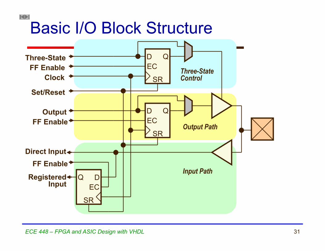
Basic I/O Block Structure
D EC
Q
SR
D EC
Q
SR
D EC
Q
SR
Three-State Control
Output Path
Input Path
Three-State
Output
Clock
Set/Reset
Direct Input
Registered Input
FF Enable
FF Enable
FF Enable

32 ECE 448 – FPGA and ASIC Design with VHDL
IOB Functionality
• IOB provides interface between the package pins and CLBs
• Each IOB can work as uni- or bi-directional I/O
• Outputs can be forced into High Impedance • Inputs and outputs can be registered
• advised for high-performance I/O • Inputs can be delayed

George Mason University ECE 448 – FPGA and ASIC Design with VHDL
Spartan-6 Family Attributes
34 ECE 448 – FPGA and ASIC Design with VHDL
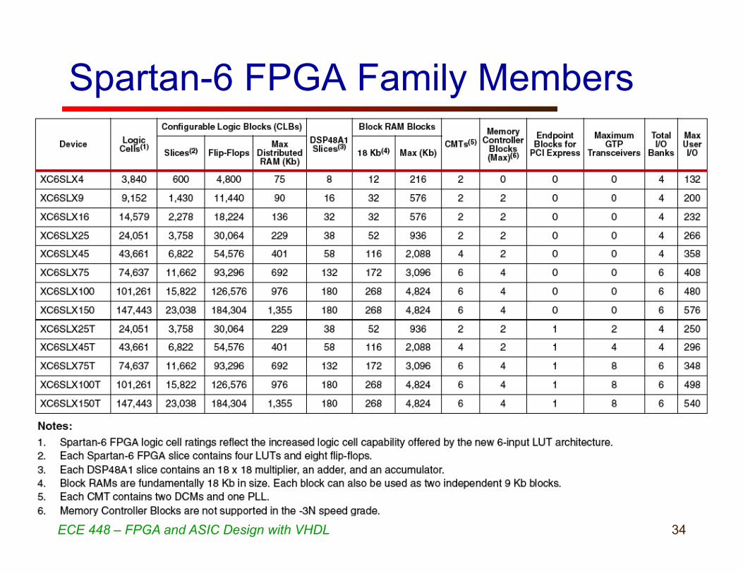
Spartan-6 FPGA Family Members

35 ECE 448 – FPGA and ASIC Design with VHDL
FPGA device present on the Digilent Nexys 3 board
XC6SLX16-CSG324C
Spartan 6 family
Size 324 pins
Package type (Ball Chip-Scale)
Commercial temperature range
0° C – 85° C
Logic Optimized

George Mason University
FPGA Design Flow

FPGA Design process (1) Design and implement a simple unit permitting to speed up encryption with RC5-similar cipher with fixed key set on 8031 microcontroller. Unlike in the experiment 5, this time your unit has to be able to perform an encryption algorithm by itself, executing 32 rounds…..
Library IEEE; use ieee.std_logic_1164.all; use ieee.std_logic_unsigned.all; entity RC5_core is port( clock, reset, encr_decr: in std_logic; data_input: in std_logic_vector(31 downto 0); data_output: out std_logic_vector(31 downto 0); out_full: in std_logic; key_input: in std_logic_vector(31 downto 0); key_read: out std_logic; ); end AES_core;
Specification / Pseudocode
VHDL description (Your Source Files) Functional simulation
Post-synthesis simulation Synthesis
On-paper hardware design (Block diagram & ASM chart)

FPGA Design process (2)
Implementation
Configuration
Timing simulation
On chip testing

39
Tools used in FPGA Design Flow
Xilinx XST
Design
Synthesis
Implementation
Xilinx ISE
VHDL code
Netlist
Bitstream
Synplify Premier
Functionally verified
VHDL code

George Mason University
Synthesis
41
Synthesis Tools
… and others
Synplify Premier Xilinx XST

42
architecture MLU_DATAFLOW of MLU is
signal A1:STD_LOGIC; signal B1:STD_LOGIC; signal Y1:STD_LOGIC; signal MUX_0, MUX_1, MUX_2, MUX_3: STD_LOGIC; begin
A1<=A when (NEG_A='0') else not A; B1<=B when (NEG_B='0') else not B; Y<=Y1 when (NEG_Y='0') else not Y1; MUX_0<=A1 and B1; MUX_1<=A1 or B1; MUX_2<=A1 xor B1; MUX_3<=A1 xnor B1; with (L1 & L0) select Y1<=MUX_0 when "00", MUX_1 when "01", MUX_2 when "10", MUX_3 when others;
end MLU_DATAFLOW;
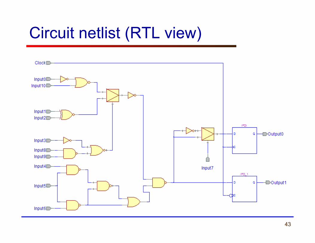
VHDL description Circuit netlist
Logic Synthesis
43
Circuit netlist (RTL view)
44
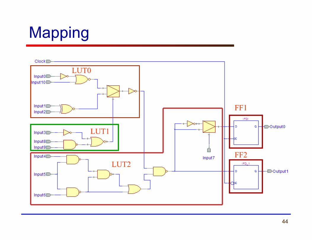
Mapping
LUT2
LUT1
FF1
FF2
LUT0

George Mason University
Implementation

46
Implementation
• After synthesis the entire implementation process is performed by FPGA vendor tools
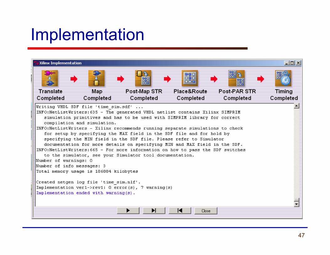
47
Implementation

48
Translation
Translation
UCF
NGD Native Generic Database file
Constraint Editor or Text Editor
User Constraint File
Circuit Netlist
Timing Constraints
Synthesis

49
Mapping
LUT2
LUT1
FF1
FF2
LUT0

50
Placing CLB SLICES
FPGA
51
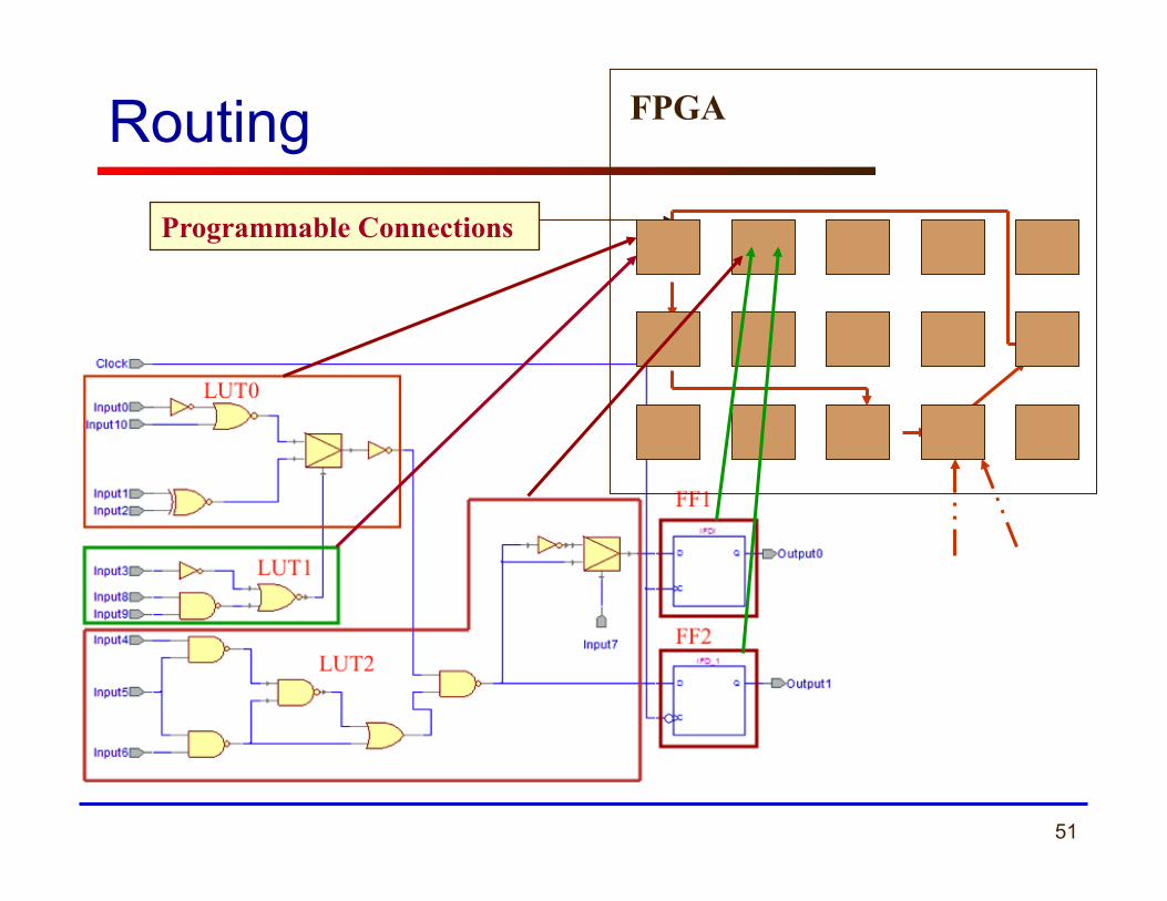
Routing Programmable Connections
FPGA
52
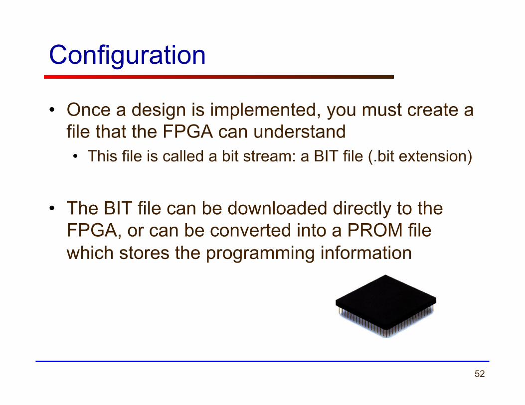
Configuration
• Once a design is implemented, you must create a file that the FPGA can understand • This file is called a bit stream: a BIT file (.bit extension)
• The BIT file can be downloaded directly to the FPGA, or can be converted into a PROM file which stores the programming information

Two main stages of the FPGA Design Flow
Synthesis
Technology independent
Technology dependent
Implementation
RTL Synthesis Map Place & Route Configure
- Code analysis - Derivation of main logic constructions - Technology independent optimization - Creation of “RTL View”
- Mapping of extracted logic structures to device primitives - Technology dependent optimization - Application of “synthesis constraints” - Netlist generation - Creation of “Technology View”
- Placement of generated netlist onto the device - Choosing best interconnect structure for the placed design - Application of “physical constraints”
- Bitstream generation - Burning device

54
Synthesis Report Example – Resource Utilization (1)
Device utilization summary: --------------------------- Selected Device : 6slx4tqg144-3 Slice Logic Utilization: Number of Slice Registers: 53 out of 4800 1% Number of Slice LUTs: 163 out of 2400 6% Number used as Logic: 163 out of 2400 6% Slice Logic Distribution: Number of LUT Flip Flop pairs used: 198 Number with an unused Flip Flop: 145 out of 198 73% Number with an unused LUT: 35 out of 198 17% Number of fully used LUT-FF pairs: 18 out of 198 9% Number of unique control sets: 7
55
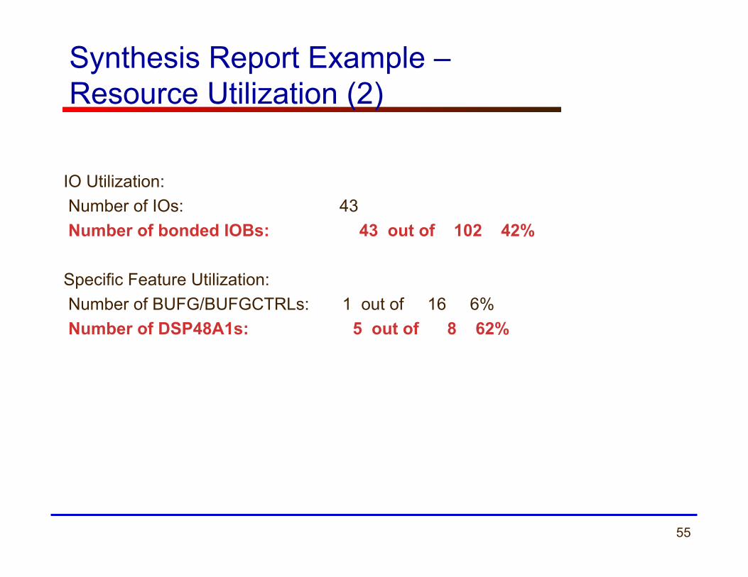
Synthesis Report Example – Resource Utilization (2)
IO Utilization: Number of IOs: 43 Number of bonded IOBs: 43 out of 102 42% Specific Feature Utilization: Number of BUFG/BUFGCTRLs: 1 out of 16 6% Number of DSP48A1s: 5 out of 8 62%

56
Synthesis Report Example – Timing
Timing Summary: --------------- Speed Grade: -3 Minimum period: 6.031ns (Maximum Frequency: 165.817MHz)
57
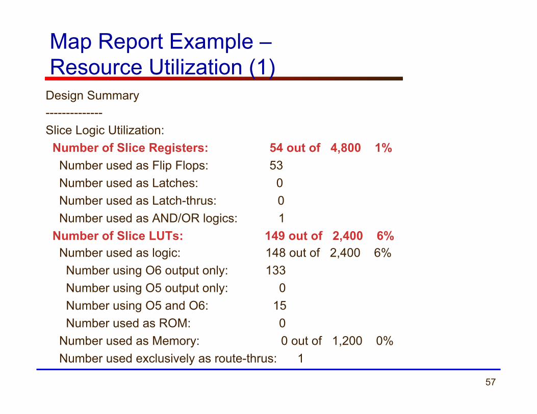
Map Report Example – Resource Utilization (1)
Design Summary -------------- Slice Logic Utilization: Number of Slice Registers: 54 out of 4,800 1% Number used as Flip Flops: 53 Number used as Latches: 0 Number used as Latch-thrus: 0 Number used as AND/OR logics: 1 Number of Slice LUTs: 149 out of 2,400 6% Number used as logic: 148 out of 2,400 6% Number using O6 output only: 133 Number using O5 output only: 0 Number using O5 and O6: 15 Number used as ROM: 0 Number used as Memory: 0 out of 1,200 0% Number used exclusively as route-thrus: 1

58
Map Report Example – Resource Utilization (2)
Slice Logic Distribution: Number of occupied Slices: 58 out of 600 9% Number of MUXCYs used: 32 out of 1,200 2% Number of LUT Flip Flop pairs used: 162 Number with an unused Flip Flop: 109 out of 162 67% Number with an unused LUT: 13 out of 162 8% Number of fully used LUT-FF pairs: 40 out of 162 24% Number of unique control sets: 7 Number of slice register sites lost to control set restrictions: 35 out of 4,800 1% IO Utilization: Number of bonded IOBs: 43 out of 102 42%

59
Map Report Example – Resource Utilization (3)
Specific Feature Utilization: Number of RAMB16BWERs: 0 out of 12 0% Number of RAMB8BWERs: 0 out of 24 0% ……. Number of DSP48A1s: 5 out of 8 62% …….

60
Post-PAR Static Timing Report
Clock to Setup on destination clock clk_i
---------------+---------+---------+---------+---------+
| Src:Rise| Src:Fall| Src:Rise| Src:Fall|
Source Clock |Dest:Rise|Dest:Rise|Dest:Fall|Dest:Fall|
---------------+---------+---------+---------+---------+
clk_i | 7.530| | | |
---------------+---------+---------+---------+---------+

61
PAR Report
----------------------------------------------------------------------------------------------------------
Constraint | Check | Worst Case | Best Case | Timing | Timing | | Slack | Achievable | Errors | Score ----------------------------------------------------------------------------------------------------------
Autotimespec constraint for clock net clk | SETUP | N/A| 7.530ns| N/A| 0 _i_BUFGP | HOLD | 0.457ns| | 0| 0
----------------------------------------------------------------------------------------------------------
62
Timing Report (1)
Timing constraint: Default period analysis for net "clk_i_BUFGP" 3354 paths analyzed, 309 endpoints analyzed, 0 failing endpoints 0 timing errors detected. (0 setup errors, 0 hold errors) Minimum period is 7.530ns. -------------------------------------------------------------------------------- Delay (setup path): 7.530ns (data path - clock path skew + uncertainty) Source: a_register/q_o_4 (FF) Destination: x_reg_inst/q_o_3 (FF) Data Path Delay: 7.453ns (Levels of Logic = 2) Clock Path Skew: -0.042ns (0.513 - 0.555) Source Clock: clk_i_BUFGP rising Destination Clock: clk_i_BUFGP rising Clock Uncertainty: 0.035ns

63
Timing Report (2) Maximum Data Path at Slow Process Corner: a_register/q_o_4 to x_reg_inst/q_o_3 Location Delay type Delay(ns) Physical Resource
Logical Resource(s)
------------------------------------------------- -------------------
SLICE_X4Y36.AQ Tcko 0.447 a_register/q_o<4>
a_register/q_o_4
DSP48_X0Y3.B4 net (fanout=21) 1.194 a_register/q_o<4>
DSP48_X0Y3.M3 Tdspdo_B_M 3.364 Mmult_mult_unsigned
Mmult_mult_unsigned
SLICE_X8Y39.C4 net (fanout=1) 2.050 mult_unsigned<3>
SLICE_X8Y39.CLK Tas 0.398 x_reg_inst/q_o<3>
Mmux_x_57
Mmux_x_4_f7_2
Mmux_x_2_f8_2
x_reg_inst/q_o_3
------------------------------------------------- --------------------
Total 7.453ns (4.209ns logic, 3.244ns route)
(56.5% logic, 43.5% route)

64
Timing Report (3)
-------------------------------------------------------------------------------- Delay (setup path): 7.484ns (data path - clock path skew + uncertainty) Source: a_register/q_o_7_1 (FF) Destination: x_reg_inst/q_o_3 (FF) Data Path Delay: 7.391ns (Levels of Logic = 2) Clock Path Skew: -0.058ns (0.513 - 0.571) Source Clock: clk_i_BUFGP rising Destination Clock: clk_i_BUFGP rising Clock Uncertainty: 0.035ns Clock Uncertainty: 0.035ns ((TSJ^2 + TIJ^2)^1/2 + DJ) / 2 + PE Total System Jitter (TSJ): 0.070ns Total Input Jitter (TIJ): 0.000ns Discrete Jitter (DJ): 0.000ns Phase Error (PE): 0.000ns
65
Timing Report (4) Maximum Data Path at Slow Process Corner: a_register/q_o_7_1 to x_reg_inst/q_o_3
Location Delay type Delay(ns) Physical Resource
Logical Resource(s)
------------------------------------------------- -------------------
SLICE_X2Y33.AQ Tcko 0.447 a_register/q_o_7_2
a_register/q_o_7_1
DSP48_X0Y3.B7 net (fanout=13) 1.132 a_register/q_o_7_1
DSP48_X0Y3.M3 Tdspdo_B_M 3.364 Mmult_mult_unsigned
Mmult_mult_unsigned
SLICE_X8Y39.C4 net (fanout=1) 2.050 mult_unsigned<3>
SLICE_X8Y39.CLK Tas 0.398 x_reg_inst/q_o<3>
Mmux_x_57
Mmux_x_4_f7_2
Mmux_x_2_f8_2
x_reg_inst/q_o_3
------------------------------------------------- --------------------
Total 7.391ns (4.209ns logic,
3.182ns route)
(56.9% logic, 43.1% route)