HybridPACK™ Drive - Infineon Technologies
52
Application Note Please read the Important Notice and Warnings at the end of this document <Revision 1.4c> www.infineon.com <2020-03-17> AN-HPD-ASSEMBLY HybridPACK™ Drive Assembly Instructions for the HybridPACK™ Drive About this document This application note describes the recommended process for mounting the HybridPACK™ Drive power module. The document is applicable to HybridPACK™ Drive power module products, listed in the section 1.1. Scope and purpose The HybridPACK™ Drive module has new assembly guiding elements which simplify positioning and alignment during the mounting process. In order to ensure a robust design meeting the high quality demands of the automotive industry, it is also important to use the right mounting order and to use appropriate printed circuit boards (PCB) material, screw types, sealing rings, etc.. The application note gives further hints and alternative screw types for high volume production. Intended audience Engineers and operators involved in the assembly of the HybridPACK™ Drive power module into power electronics systems. Table of Contents 1 General Information....................................................................................................... 3 1.1 HybridPACK™ Drive product list in scope of this application note........................................................ 4 2 Recommended Mounting Order ....................................................................................... 5 3 PressFit Assembly .......................................................................................................... 6 3.1 Requirements for the PCB....................................................................................................................... 6 3.2 General hints for the PCB Footprint ....................................................................................................... 9 3.3 Press-In Tools ........................................................................................................................................ 10 3.4 Press-In Process .................................................................................................................................... 13 3.4.1 PCB alignment before the press-in process .................................................................................... 13 3.4.1 Press-in process description............................................................................................................ 13 3.4.1 Typical press-in example with dF stop criteria ............................................................................... 15 3.4.2 Alternative: Press-In Process with distance keeper ........................................................................ 16 4 Soldering Modules (alternative to PressFIT) .................................................................... 17 4.1 Requirements for the PCB for soldering ............................................................................................... 17 4.2 Solder Tools ........................................................................................................................................... 18 4.3 Solder Process ....................................................................................................................................... 18 4.4 Typical solder process example............................................................................................................ 19 5 PCB Design hint for high thermal cycle system robustness ................................................ 21 5.1 PCB stiffness/spring force characterization ......................................................................................... 21 5.2 PCB slots for spring force reduction ..................................................................................................... 22 5.2.1 Typical PCB Footprint with slots ..................................................................................................... 24 5.3 PCB design for module external mounting .......................................................................................... 24 6 Power Module Cooling System ....................................................................................... 26 6.1 Reference Cooler Design ....................................................................................................................... 26 6.2 Recommendation for the sealing ring .................................................................................................. 29 6.3 Cooling fluid .......................................................................................................................................... 31 7 Screw types and processes ............................................................................................ 32
Transcript of HybridPACK™ Drive - Infineon Technologies

Application Note Please read the Important Notice and Warnings at the end of this document <Revision 1.4c>
www.infineon.com <2020-03-17>
AN-HPD-ASSEMBLY
HybridPACK™ Drive Assembly Instructions for the HybridPACK™ Drive
About this document
This application note describes the recommended process for mounting the HybridPACK™ Drive power module.
The document is applicable to HybridPACK™ Drive power module products, listed in the section 1.1.
Scope and purpose
The HybridPACK™ Drive module has new assembly guiding elements which simplify positioning and alignment
during the mounting process. In order to ensure a robust design meeting the high quality demands of the
automotive industry, it is also important to use the right mounting order and to use appropriate printed circuit
boards (PCB) material, screw types, sealing rings, etc.. The application note gives further hints and alternative
screw types for high volume production.
Intended audience
Engineers and operators involved in the assembly of the HybridPACK™ Drive power module into power
electronics systems.
Table of Contents
1 General Information....................................................................................................... 3 1.1 HybridPACK™ Drive product list in scope of this application note ........................................................ 4
2 Recommended Mounting Order ....................................................................................... 5
3 PressFit Assembly .......................................................................................................... 6
3.1 Requirements for the PCB ....................................................................................................................... 6 3.2 General hints for the PCB Footprint ....................................................................................................... 9 3.3 Press-In Tools ........................................................................................................................................ 10
3.4 Press-In Process .................................................................................................................................... 13
3.4.1 PCB alignment before the press-in process .................................................................................... 13 3.4.1 Press-in process description ............................................................................................................ 13 3.4.1 Typical press-in example with dF stop criteria ............................................................................... 15
3.4.2 Alternative: Press-In Process with distance keeper ........................................................................ 16
4 Soldering Modules (alternative to PressFIT) .................................................................... 17
4.1 Requirements for the PCB for soldering ............................................................................................... 17 4.2 Solder Tools ........................................................................................................................................... 18 4.3 Solder Process ....................................................................................................................................... 18
4.4 Typical solder process example ............................................................................................................ 19
5 PCB Design hint for high thermal cycle system robustness ................................................ 21
5.1 PCB stiffness/spring force characterization ......................................................................................... 21 5.2 PCB slots for spring force reduction ..................................................................................................... 22
5.2.1 Typical PCB Footprint with slots ..................................................................................................... 24 5.3 PCB design for module external mounting .......................................................................................... 24
6 Power Module Cooling System ....................................................................................... 26
6.1 Reference Cooler Design ....................................................................................................................... 26 6.2 Recommendation for the sealing ring .................................................................................................. 29
6.3 Cooling fluid .......................................................................................................................................... 31
7 Screw types and processes ............................................................................................ 32

Application Note 2 <Revision 1.4c>
<2020-03-17>
HybridPACK™ Drive Assembly Instructions for the HybridPACK™ Drive
General Information
7.1 Baseplate Mounting Screws .................................................................................................................. 32 7.1.1 Alternative: self-tapping screws for baseplate mounting .............................................................. 33
7.2 Fixation/clamping of the module during the baseplate screw process .............................................. 35 7.3 PCB mounting screws on the module housing .................................................................................... 36
7.4 Screw Orders (Baseplate and PCB) ....................................................................................................... 37
8 Connecting to the Power Terminals ................................................................................ 38
8.1 Mounting Options .................................................................................................................................. 38 8.1.1 Additional Information for Welding Processes ............................................................................... 39
8.2 Forces on Power Tabs ........................................................................................................................... 40
9 System Assembly Clearance & Creepage Distances ........................................................... 41
10 Phase Current Sensor Integration ................................................................................... 42
11 Traceability, Data Matrix and Part Markings .................................................................... 43
12 Technical Drawing ........................................................................................................ 44
12.1 Basic Explanation Coordinate System ................................................................................................. 44 12.2 Pin Position and Pin Gauge ................................................................................................................... 45
13 Storage and Transport .................................................................................................. 47
14 Power Module Appearance............................................................................................. 48
14.1 Pin Rotation ........................................................................................................................................... 48 14.2 Module Lid to PCB Distance .................................................................................................................. 48
14.3 Power Tab Tin Plating ........................................................................................................................... 49 14.4 Baseplate Surface .................................................................................................................................. 49
15 References and Revision History .................................................................................... 50
Application Note 3 <Revision 1.4c>
<2020-03-17>
HybridPACK™ Drive Assembly Instructions for the HybridPACK™ Drive
General Information
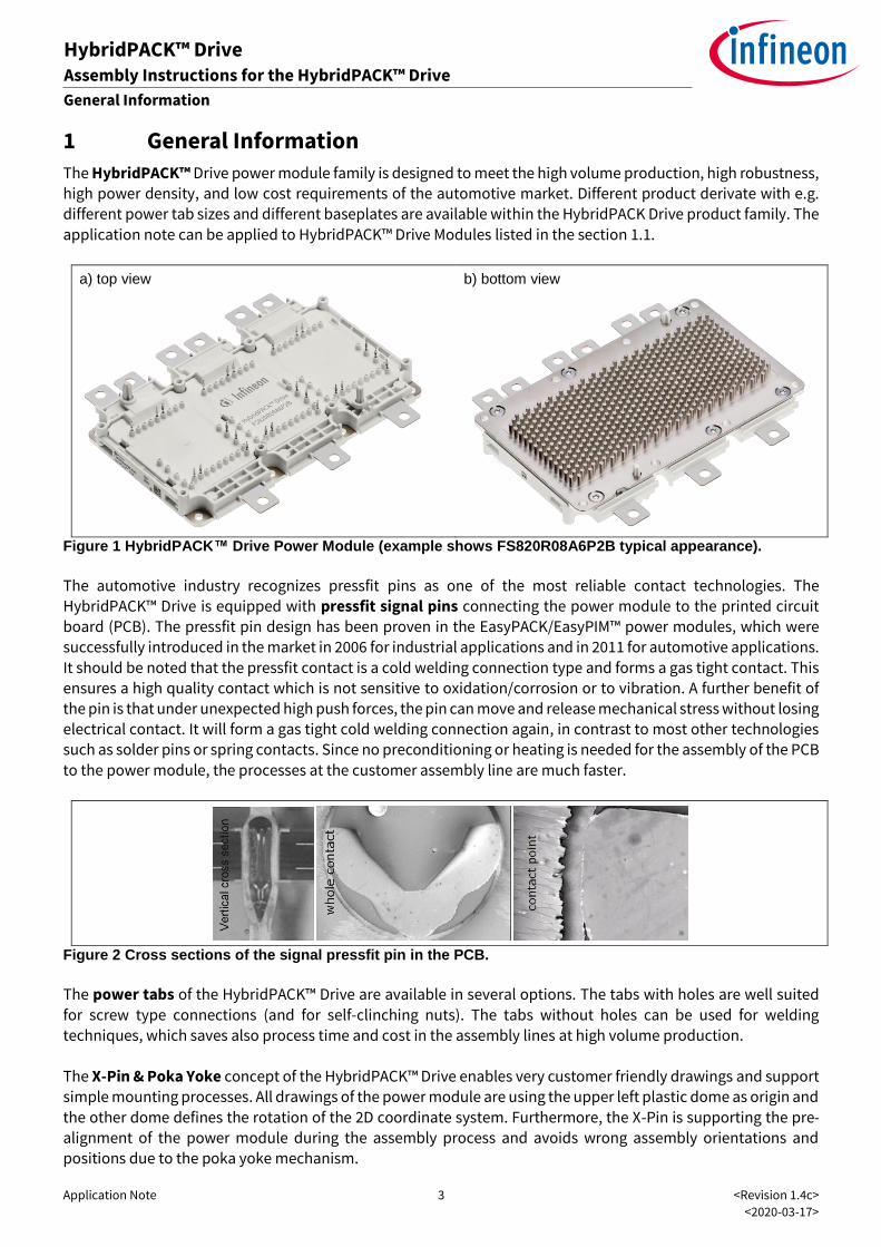
1 General Information
The HybridPACK™ Drive power module family is designed to meet the high volume production, high robustness, high power density, and low cost requirements of the automotive market. Different product derivate with e.g. different power tab sizes and different baseplates are available within the HybridPACK Drive product family. The
application note can be applied to HybridPACK™ Drive Modules listed in the section 1.1.
a) top view
b) bottom view
Figure 1 HybridPACK™ Drive Power Module (example shows FS820R08A6P2B typical appearance).
The automotive industry recognizes pressfit pins as one of the most reliable contact technologies. The
HybridPACK™ Drive is equipped with pressfit signal pins connecting the power module to the printed circuit board (PCB). The pressfit pin design has been proven in the EasyPACK/EasyPIM™ power modules, which were
successfully introduced in the market in 2006 for industrial applications and in 2011 for automotive applications.
It should be noted that the pressfit contact is a cold welding connection type and forms a gas tight contact. This
ensures a high quality contact which is not sensitive to oxidation/corrosion or to vibration. A further benefit of the pin is that under unexpected high push forces, the pin can move and release mechanical stress without losing electrical contact. It will form a gas tight cold welding connection again, in contrast to most other technologies
such as solder pins or spring contacts. Since no preconditioning or heating is needed for the assembly of the PCB
to the power module, the processes at the customer assembly line are much faster.
Figure 2 Cross sections of the signal pressfit pin in the PCB.
The power tabs of the HybridPACK™ Drive are available in several options. The tabs with holes are well suited
for screw type connections (and for self-clinching nuts). The tabs without holes can be used for welding techniques, which saves also process time and cost in the assembly lines at high volume production.
The X-Pin & Poka Yoke concept of the HybridPACK™ Drive enables very customer friendly drawings and support simple mounting processes. All drawings of the power module are using the upper left plastic dome as origin and
the other dome defines the rotation of the 2D coordinate system. Furthermore, the X-Pin is supporting the pre-alignment of the power module during the assembly process and avoids wrong assembly orientations and positions due to the poka yoke mechanism.

Application Note 4 <Revision 1.4c>
<2020-03-17>
HybridPACK™ Drive Assembly Instructions for the HybridPACK™ Drive
General Information
Figure 3 X-Pin & Poka Yoke in the HybridPACK™ Drive power module enables simple mounting processes.
1.1 HybridPACK™ Drive product list in scope of this application note
The scope of the application note is for the following products:
Type Designation SP order number Status
FS660R08A6P2FB SP001632426 in production
FS660R08A6P2FLB SP001850450 in production
FS770R08A6P2B SP001706976 in production
FS770R08A6P2LB SP001987412 in production
FS820R08A6P2B SP001499708 in production
FS820R08A6P2LB SP001611366 in production
FS820R08A6P2 SP001499702 in production Product not listed? Please ask your Infineon sales representative.

Application Note 5 <Revision 1.4c>
<2020-03-17>
HybridPACK™ Drive Assembly Instructions for the HybridPACK™ Drive
Recommended Mounting Order
2 Recommended Mounting Order
All datasheet drawings specify the power module at the state of delivery. Deformations on the product can occur when the power module is mounted to a cooling system (i.e. depending on cooler flatness and screw torque). As the pin position tolerance is important for PCB assembly, it is recommended to press the PCB on the power
module first, and assemble the power module into the cooling system next. In order to avoid putting unnecessary mechanical stress on the PCB, it should be fixed by screws on the power module subsequent to mounting the power module to the cooling system.
As a summary, the following mounting order can be recommended:
1. Align PCB to the power module (the X-Pins will support this process).
2. Press-in PCB (recommended is controlled way-force press-in process).
3. Prepare cooling system with the sealing ring.
4. Attach power module with PCB to the prepared cooling system.
5. Fix module baseplate on the cooler by screws.
6. Fix the PCB on the power module by screws.
7. Connect the module power tabs to busbar, capacitor, etc.
When self-clinching nuts are chosen for the connecting type of the module power tabs it is recommended to press-in these nuts in the assembly line before the PCB mounting step 1 starts.

Application Note 6 <Revision 1.4c>
<2020-03-17>
HybridPACK™ Drive Assembly Instructions for the HybridPACK™ Drive
PressFit Assembly
3 PressFit Assembly
3.1 Requirements for the PCB
The pressfit technology used in the HybridPACK™ Drive is designed based on IEC 60352-5 for standard FR4 printed
circuit boards with immersion tin plating. The PCB material must be compliant with IEC 60249-2-4 or IEC 60249-2-5 for double-sided printed circuit boards and IEC 60249-2-11 or IEC 60249-2-12 for multilayer printed circuit
boards. The requirements for the PCB are in Table 1. In case the requirements are not met, there is risk of a not gas tight signal pin connection or of pin and/or PCB via damage. The recommendations for the PCB for the X-pin holes
are in Table 2.
Please note that the pressfit hole specifications are only valid for assembled PCBs. In case of unassembled PCBs,
e.g. for testing purposes, it is recommended to perform a standard reflow solder process before starting the power module assembly process.
Table 1 Requirements to the PCB.
No Description Unit min. typ. max. Remarks and known common mistakes
1 Drill tool diameter mm 1.12 1.15 Wrong drill tool applied. Specify clearly the
pressfit hole positions and required drill
tool size to the PCB manufacturer.
2 Copper thickness in hole um 25 50 In case the via metallization is lower than
specification, the risk is a damaged/cracked
via.
3 End hole diameter mm 1.02 1.10 End hole diameters lower than spec may
lead to increased press-in forces (typically
>115 N per pin) and may damage the pins.
Larger holes than spec may lead to low
press-in forces (typically <40 N per pin) and
can cause not gas tight connections.
4 Copper thickness of conductors um 35 70
105
400 No results available for thinner or thicker
copper layers.
5 Hole to hole pattern tolerance um ±100 In typical PCB manufacturing hole to hole
pattern is lower than ±80um.
6 Recommended PCB thickness mm 1.6 Target value with +/-10% thickness
tolerance
7 Recommended max PCB spring
force in characterization (see
chapter 5)
N/mm 450 For high thermal cycle system robustness it
is recommended to limit PCB stiffness (i.e.
spring force). See chapter 5 for more
information.
8 Metallization of circuit board Immersion Tin
(Sn chemically)
Immersion tin has typ 1-5um metallization
in the hole. Other metallization type should
be avoided can lead to strong deviation in
press-in forces. E.g. HAL leadless show high
variations in press-in forces and risk is a not
gas tight pin connection, which can fail over
application lifetime. PCB with ENIG plating
can lead to increased press forces due to
hard surface and this PCB type was not
tested at Infineon module qualification
tests.
9 Metallization of pin Ni/Sn (galvanic) The Sn plated pin with nickel under layer
avoids potential whisker growth out of the
upper galvanic tin layer.

Application Note 7 <Revision 1.4c>
<2020-03-17>
HybridPACK™ Drive Assembly Instructions for the HybridPACK™ Drive
PressFit Assembly
Table 2 Recommendations for the printed circuit board X-pin holes
No Description unit min. typ. max. Remark
1 End hole diameter X-Pin1
mm 5.82 5.90 The hole should be drilled with 6.0mm drill
tool and not milled in order to avoid
additional unnecessary hole position
tolerances.
2 End hole diameter
Y-Pin1
mm 4.82 4.90 The hole should be drilled with 5.0mm drill
tool and not milled in order to avoid
additional unnecessary hole position
tolerances. 3 Hole to hole pattern tolerance um ±100 Plated holes are preferred in order to
achieve a minimum “X-pin hole” to “pressfit
hole” pattern tolerance.
Please take note that the PCB pressfit holes should not be specified just by the finished end hole diameter. The risk is that wrong processes are applied by the PCB manufacturer. Please give your PCB manufacturer the information that all holes for the signal pins must be manufactured according to Table 1. As PCB design tools
typically do not differentiate between “normal” and “pressfit holes” it is a well-known workaround to use a
“unique hole size e.g. 1.06mm” in the PCB design for all pressfit holes. Then the pressfit holes are separate in the NC drill files and thus the PCB manufacturer knows exactly the positions where to apply the spec according to
Table 1. An example for such a workaround is shown in Figure 4. Experience has shown that it is best practice to place additionally a text on the drill drawing layer, where it is
clearly specified that the 1.06mm holes are the pressfit holes according to the specification of Table 1. This text is also visible in the gerber files which are the typical exchange format between the PCB designer and the manufacturer. Figure 19 show an example of such a recommended footprint.
NCDrill File Report
---------------------------------------------------------------------------
Layer Pair : Top Layer to Bottom Layer
Tool Hole Size Hole Type Hole Count Plated Tool Travel
---------------------------------------------------------------------------
T1 1.1mm (39.37mil) Round 24 543.04 mm (21.38 Inch)
T2 1.06mm (42.13mil) Round 24 428.69 mm (16.88 Inch) SEE PRESSFIT SPEC!
T3 3.6mm (141.732mil) Round 8 459.55 mm (18.09 Inch)
T4 4mm (157.48mil) Round 4 635.11 mm (25.00 Inch)
T5 4.9mm (192.913mil) Round 1 0.00 mm (0.00 Inch)
T6 5.9mm (232.283mil) Round 1 0.00 mm (0.00 Inch)
T7 10mm (393.701mil) Round 8 NPTH 447.98 mm (17.64 Inch)
---------------------------------------------------------------------------
Figure 4 Example NC Drill File (tool header only) of a PCB design where all pressfit holes are specified with 1.06mm and a note to the manufacturer is added. The PCB manufacturer can now easily distinguish between a normal and a pressfit hole (see tool T2).
1 Experience has shown that PCB hole diameter should be significantly larger than the module frame element for a seamless assembly
process. The given relative large hole diameters in the PCB is the best compromise between Module and PCB alignment and the
necessary play during this assembly step. The specified relative large hole sizes avoid an unnecessary rotation of the PCB with
respect to the signal pin coordinate system.

Application Note 8 <Revision 1.4c>
<2020-03-17>
HybridPACK™ Drive Assembly Instructions for the HybridPACK™ Drive
PressFit Assembly
A structure of a PCB according to the spec in Table 1 is illustrated in Figure 5. The hole in the PCB is drilled with a drill tool size of 1.15 mm. It is normal that PCB material shrinks after drilling. Therefore, this shown hole size with
1.15mm should not be understood as a check gauge after drilling rather than an illustration for understanding the PCB stack.
Later in the process, the holes will be plated. It is important to have minimum 25um copper in the hole otherwise the press forces may damage/crack the via. According to experience, larger annular rings are typically more
robust to mechanical forces and thus large annular rings (e.g. 0.5 mm) should be used wherever possible in the design.
The metallization/plating in the holes has to be manufactured in an immersion tin (i.e. chemical tin) process. This process is known to generate very uniform layer thicknesses (typically about 1um) and ensures the correct press-in forces as well as an appropriate contact surface for achieving gas tight pressfit connections.
Figure 5 Structure of a PCB according to the specification in Table 1.
1.15 mm*
1.15 mm*
min. 25 µm Cu; max. 50 µm Cu
immersion tin typ. 1 µm (max 15 um)
min 1.02 mm
max 1.10 mm
Drill hole
Copper in hole
End hole diameter
min 1.02 mm
max 1.10 mm
*measurement after process can show lower values due to PCB shrinking. Value indicates drill tool size.

Application Note 9 <Revision 1.4c>
<2020-03-17>
HybridPACK™ Drive Assembly Instructions for the HybridPACK™ Drive
PressFit Assembly
3.2 General hints for the PCB Footprint
PCB footprint typically depend on PCB manufacturing processes and customer specific design rules. The
following table can be understood as a best practice and starting point for system design. Table 3 Hint for PCB footpint holes. PCB bottom layer is defined on side of the power module.
No Type PCB Implementation Hint
1 X-Pin holes Hole at 0/0 Position*
End hole Diameter: 5.90 mm (see Table 2) Top Layer Copper Diameter: >= 6.40 mm
Mid Layer Copper Diameter: >= 6.40 mm Bottom Layer Copper Diameter: >= 8.00mm
Hole at 87/82 Position* End hole Diameter: 4.90 mm (see Table 2) Top Layer Copper Diameter: >= 5.40 mm Mid Layer Copper Diameter: >= 5.40 mm
Bottom Layer Copper Diameter: >= 8.00mm
2 Signal pressfit pin holes See Table 1
3 Components Keepout around pressfit Pins
Uncritical packages like SO, TSSOP, QFP or not safety relevant SMD resistors: >=3mm radius from the hole center
Others:
>=4mm radius from the hole center
4 PCB fixing screw holes End hole Diameter: 3.60 mm
Top Layer Copper Diameter: >= 7.00 mm Mid Layer Copper Diameter: >= 6.50 mm
Bottom Layer Copper Diameter: >= 6.60 mm *: The x-pin holes can be designed both as plated or un-plated holes. Plated holes with annular rings as noted in the table are the preferred
solution. All plated holes are drilled at the PCB manufacturers within the same process and leads to best hole to hole pattern tolerances
as a consequence.

Application Note 10 <Revision 1.4c>
<2020-03-17>
HybridPACK™ Drive Assembly Instructions for the HybridPACK™ Drive
PressFit Assembly
3.3 Press-In Tools
This chapter describes a sample press-in tool, which can be adapted to project specific details like PCB assembly
locations, maximum height of other PCB parts, etc. to avoid mechanical collisions during the press-in process. The press-in tool is made of two parts (see Figure 6).
Figure 6 Press-tool example.
The bottom tool supports the power module baseplate and has to avoid damage of the pin-fin cooling area. The material and/or plating of the bottom part of the tool has to be selected in order to avoid scratches and damage
of the baseplate sealing area. The holes for the X-pins avoid, by the poka yoke concept, a wrong orientation of the power module in the press-tool.
The top tool supports the PCB around the pressfit pins with cylindrical shapes and support the PCB during the during the press-in process. This part of the tool should be made of material, which can withstand the press-in
forces. The top tool also has cylindrical shapes around the X-pins in order to avoid a press-in process with an incorrectly oriented tool or power module.
Please note that the top tool height (height of the cylinders) must be adjusted according to the maximum PCB assembly height. Collision of PCB top side assembly must be avoided.
A mechanical drawing of the sample press-in tools is given in Figure 7 and Figure 8, and a 3D step model can be
obtained from Infineon Technologies on request.

Application Note 11 <Revision 1.4c>
<2020-03-17>
HybridPACK™ Drive Assembly Instructions for the HybridPACK™ Drive
PressFit Assembly
Edges: ISO 13715; Tolerance: ISO 2768 – mK; Surface: EN ISO 1302; Material: 1.4301 (V2A) Figure 7 Technical drawing of the sample press-in tool (Top Tool).
The standoffs for the 8 domes are designed in the press tool higher than the area for the 24 pins. This staged tool avoid or significantly reduces pull forces on the signal pins in the final assembly. The recommended staged tool lead to a mechanical robust assembly at minimized module stress.
(zoom)

Application Note 12 <Revision 1.4c>
<2020-03-17>
HybridPACK™ Drive Assembly Instructions for the HybridPACK™ Drive
PressFit Assembly
Edges: ISO 13715; Tolerance: ISO 2768 – mK; Surface: EN ISO 1302; Material: ABS plastic
Figure 8 Technical drawing of the sample press-in tool (Bottom Tool).
The bottom tool can protect the underside of the IGBT module (especially the PinFin and sealing area) against
damage/scratching during the press-in process.
The press-tool can be used in a simple toggle lever press for engineering purpose or in a controlled machine for
serial production.

Application Note 13 <Revision 1.4c>
<2020-03-17>
HybridPACK™ Drive Assembly Instructions for the HybridPACK™ Drive
PressFit Assembly
3.4 Press-In Process
3.4.1 PCB alignment before the press-in process
The PCB can be assembled to the power module only in a correct orientation due to the poka-yoke mechanism
of the X-pins. The PCB has to be positioned with a manual or automated handling tool to the X-pins without tilt. It is recommended to design a handling tool, which enables a significant play of the PCB in x-y direction. During the positioning of the PCB to the module the soft and round shaped X-pins will guide the PCB to the right position before the PCB will touch the pins. The signal pins itself will do kind of a “fine-alignment” while moving the PCB
further down to the module. A low force in the range up to 10..20N in z-axis is allowed on the PCB to support the
final alignment process. In final position (before the press-in process) the signal pins will appear clearly at the PCB topside for 1.6mm thick PCBs. The system is ready for the press-in process when all pins are correctly inserted. They also appear on the topside
of PCB. This status can be checked e.g. manually, by automatic optical inspection (AOI) or PCB height level (see Figure 9 for typical appearance after correct PCB alignment process).
A)
B)
Figure 9 PCB at beginning of alignment process (A). After correct alignment, the pins are inserted in the PCB and are clearly visible at the PCB top side (B). The system is now ready for the press-in process.
3.4.1 Press-in process description
The press-in process is recommended with a controlled force-distance method for serial production. For testing under laboratory conditions, a manual toggle-press also typically gives good results.

Application Note 14 <Revision 1.4c>
<2020-03-17>
HybridPACK™ Drive Assembly Instructions for the HybridPACK™ Drive
PressFit Assembly
Figure 10 Typical way-force press-in diagram from a HybridPACK™ Drive module FS820R08A6P2B with 24 signal pins.
The Figure 10 show an example of a HybridPACK Drive press-in process. The press-in process starts when the force increases. At this point the z-axis is set to 0 mm in this diagram. In case an initial high peak is detected it may indicate a failure in the process like PCB hole plugged with solder, not properly inserted PCB before the process starts, machine collision with other external parts, etc.
The force curve will increase smoothly while pressing down the PCB (see diagram 0 to 1.6mm). This force curve
will have same appearance for different press-in speeds. Lower press-in speeds as noted in Table 4 are not allowed as the press-in forces can increase and damage the pin. Higher press-in speeds are uncritical for the module. The maximum speed is noted with respect to press-in equipment limitation. A higher speed was not tested and can therefore not recommended.
Considering the 1st derivative of the force-distance diagram (see dForce diagram) a significant slope change can
be detected at the end of the process (in the example at about z=1.6mm). At this point the PCB is fully pressed on the module housing and the effective part of the press-in process is done. At this point the force should be minimum 40N per pin (i.e. 960N for HybridPACK Drive with 24 pins) in the example the effective pin force was
1.4kN. Ideally the press-in process should be stopped as soon as this point is detected (i.e. dF stop critera). With the dForce curve it is also possible to record the effective press-length, which should be more than 0.9mm
to ensure that pins have sufficient overlap with the PCB vias. In the example the effective press-in depth was about 1.6mm.
After the slope changing point, the PCB is already in contact with the module housing. Further pressing down increases the force on the housing. It is always beneficial to detect the slope changing point and to stop the press-in process as soon as this point is detected. The reason is that the additional force is unnecessary for the pin

Application Note 15 <Revision 1.4c>
<2020-03-17>
HybridPACK™ Drive Assembly Instructions for the HybridPACK™ Drive
PressFit Assembly
contact, which is already fully pressed-in and additional force only create unnecessary stress on the module housing.
A general spec on how to detect the slope changing point is hardly possible because it is also machine, speed, PCB, etc dependent. In the shown example the point is nearly in the area where dForce/way raises above 4kN per
mm which is much higher dForce/way compared to the effective press-in area before (about up to 1.5kN per mm).
Please note it is important that the press-in equipment is designed for the expected high forces. During the press-in process the bottom and top press tool must be parallel to each other and should be mechanically fixed without
tilt. Table 4 Overview press-in process
No Description unit min. typ. max. Remarks
1 Press-in speed mm/s 0.4 2..4 8 During the press-in process it is not
allowed to come under the minimum
speed (no multistep press-in process).
The maximum press-in speed is
typically limited due to non ideal press
machine. See explanation “stop
criteria”
2 Max allowed press force on module
kN dF stop criteria
dF stop criteria
3.5
the press-in process should be stopped
when the slope change point is
detected (effective press-in done, see
Figure 10). The force recording speed,
machine stop behavior has to be also
taken into account for proper setting
the “stop criteria”. See also section
3.4.1.
3 Recommended effective press-in length
mm 0.9 The pin might be also gas tight at lower
effective press-in length in case
sufficient force was applied.
Explanation on “stop criteria” and maximum recommended press-in speed:
Please ensure that press machine has fast enough force recording and can stop the tool travel fast enough (i.e. consideration of machine delay). A real press machine has limited bandwidth on force recording. After stop command the machine may take
time until tool travel is really stopped. Both lead to a so called machine delay.
At end of the press-in process, where PCB come in contact to the mounting domes a load of about 1000N per 0.1mm (10kN/mm) tool travel can be expected.
3.4.1 Typical press-in example with dF stop criteria
Figure 11 shows an example of different assembly tests with the recommended dF stop criteria. Different PCB
designs from different PCB suppliers were applied in this experiment. Despite same machine parameters were
applied it can be clearly seen that the press-in process is stopped as soon as the slope changing point is detected were the effective press-in process is done. For group A higher press-in way and higher press-in force was necessary compared to group C, but with dF stop criteria the tool travel is stopped always close to the
individual ideal point. At end of the process it can be checked if all parameters were OK, e.g. if minimum press-in force was reached and maximum allowed force not exceeded as well as if the minimum recommended
effective press-in length was reached.

Application Note 16 <Revision 1.4c>
<2020-03-17>
HybridPACK™ Drive Assembly Instructions for the HybridPACK™ Drive
PressFit Assembly
Figure 11 Typical press-in example with the recommended dF stop criteria. FS820R08A6P2B modules were assembled with Harting CPM prestige press machine [2]. Different PCB layouts from different PCB suppliers (PCB group A to C) were tested.
3.4.2 Alternative: Press-In Process with distance keeper
Especially for system design where PCB is larger than the power module it can be a major advantage to use a modified press-in tool with a distance keeper and to fix later the PCB directly at the inverter not the module
housing (see section 5.3 for more details).
Adjusting for such a press-in approach following items have to be considered.
Press-tool distance keeper (1) should be designed at the positions of the 8x module baseplate holes.
Press-tool distance keeper (1) should have a minimum 8mm diameter.
Maximum force press-in force of 3.5kN should not be exceeded.
Press-tool distance keeper height: Gap between PCB and module housing domes should be at least
100um after the press-in process.
Figure 12 Sample press tool with distance keeper.

Application Note 17 <Revision 1.4c>
<2020-03-17>
HybridPACK™ Drive Assembly Instructions for the HybridPACK™ Drive
Soldering Modules (alternative to PressFIT)
4 Soldering Modules (alternative to PressFIT)
The HybridPACK Drive signal pin was originally designed for press-in process. Experience has shown that the tin plated pin with nickel underlayer is also suited for selective solder process. This chapter gives a guideline how to solder the HybridPACK Drive modules properly. Press-in and soldering should not be performed subsequently.
The described soldering is only an alternative mounting option to pressfit and should not be seen as a replacement for it. Furthermore, a solder process does not lead to higher robustness and requires much longer process times in the assembly line.
4.1 Requirements for the PCB for soldering
For soldering the signal pins it is required to specify the PCB slightly different. The list of requirements can be
seen in Table 5. The general hints for the PCB footprint can be fully transferred from section 3.2 also in the case
of soldering the modules. Table 5 Requirements to the PCB for soldering process.
No Description Unit min. typ. max. Remarks
1 End hole diameter mm 1.5 1.55 1.6 Other hole sizes might be possible but were
not tested.
2 Copper thickness in hole um 25 50
3 Copper thickness of conductors um 35 70
105
400
4 Hole to hole pattern tolerance um ±100 In typical PCB manufacturing hole to hole
pattern is lower than ±80um.
5 Recommended PCB thickness mm 1.6 Target value with +/-10% thickness
tolerance
6 Recommended max PCB spring
force in characterization (see
chapter 5)
N/mm 450 For high thermal cycle system robustness it
is recommended to limit PCB stiffness (i.e.
spring force). See chapter 5 for more
information.
7 Metallization of circuit board Immersion Tin (Sn chemically)
OR HAL leadless
ENIG might be also possible but was not
tested.
8 Metallization of pin Ni/Sn (galvanic) The Sn plated pin with nickel under layer
avoids potential whisker growth out of the
upper galvanic tin layer.
Application Note 18 <Revision 1.4c>
<2020-03-17>
HybridPACK™ Drive Assembly Instructions for the HybridPACK™ Drive
Soldering Modules (alternative to PressFIT)
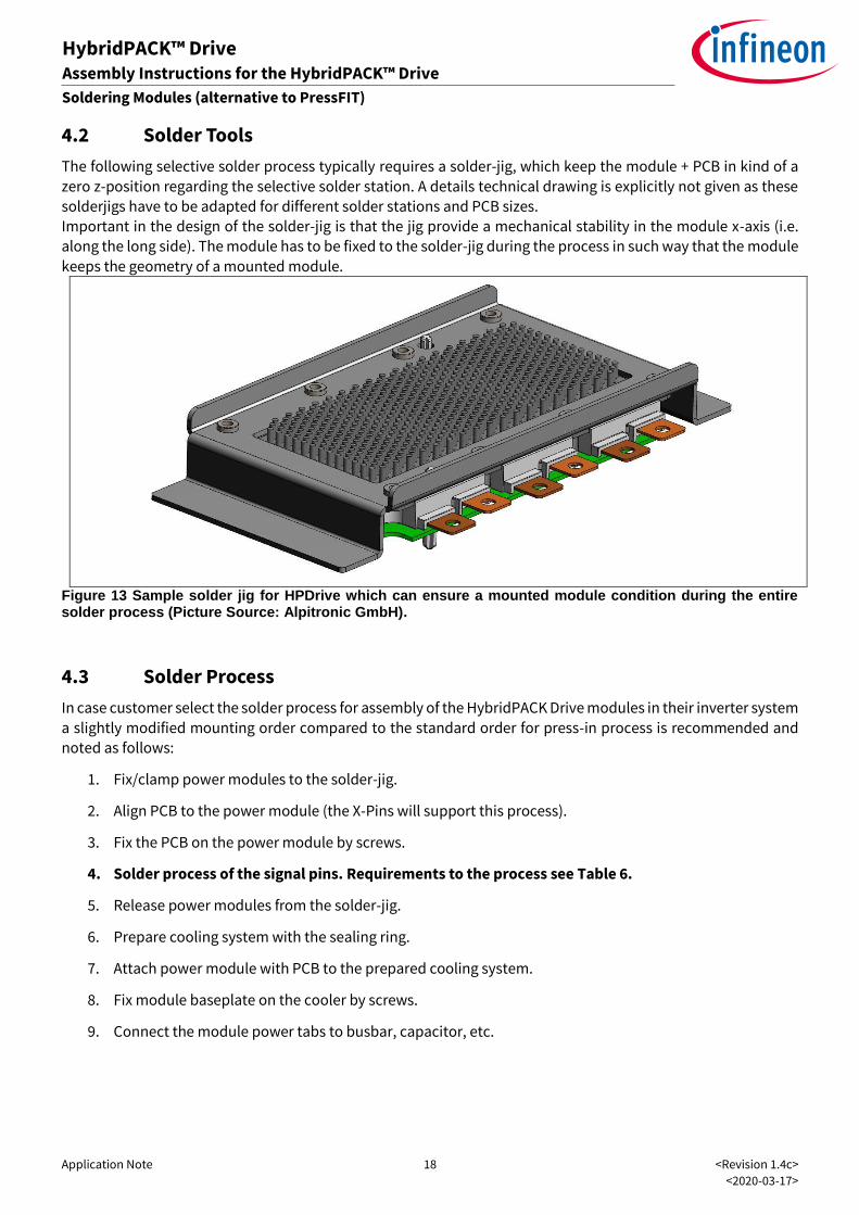
4.2 Solder Tools
The following selective solder process typically requires a solder-jig, which keep the module + PCB in kind of a
zero z-position regarding the selective solder station. A details technical drawing is explicitly not given as these solderjigs have to be adapted for different solder stations and PCB sizes.
Important in the design of the solder-jig is that the jig provide a mechanical stability in the module x-axis (i.e. along the long side). The module has to be fixed to the solder-jig during the process in such way that the module
keeps the geometry of a mounted module.
Figure 13 Sample solder jig for HPDrive which can ensure a mounted module condition during the entire solder process (Picture Source: Alpitronic GmbH).
4.3 Solder Process
In case customer select the solder process for assembly of the HybridPACK Drive modules in their inverter system
a slightly modified mounting order compared to the standard order for press-in process is recommended and noted as follows:
1. Fix/clamp power modules to the solder-jig.
2. Align PCB to the power module (the X-Pins will support this process).
3. Fix the PCB on the power module by screws.
4. Solder process of the signal pins. Requirements to the process see Table 6.
5. Release power modules from the solder-jig.
6. Prepare cooling system with the sealing ring.
7. Attach power module with PCB to the prepared cooling system.
8. Fix module baseplate on the cooler by screws.
9. Connect the module power tabs to busbar, capacitor, etc.

Application Note 19 <Revision 1.4c>
<2020-03-17>
HybridPACK™ Drive Assembly Instructions for the HybridPACK™ Drive
Soldering Modules (alternative to PressFIT)
Table 6 Requirements for selective solder process.
No Description Unit min. typ. max. Remarks
1 Solder peak temperature of pins
(Tp) Solder time at Tp
°C
s
260..280
10..5
2 Maximum local module housing
temperature
°C 223 Hot spot at the module lid close to the pin
up to maximum local module housing
temperature allowed. The entire volume
should not exceed 150°C. See also
temperature spec at the module domes
3 Module dome temperature
during solder TL
°C 100 150 TL: The time where the solder at the pins is
above its liquidous temperature.
This ensure that the PCB is fixed at position
where module domes are in expanded
condition.
4 Module mounted - yes Module should to be clamped/fixed to an
appropriate solder-jig that its keeps the
geometry like in a mounted condition.
4.4 Typical solder process example
In this section an example of a solder process as described in the previous sections is shown. Customer can adjust this process within the specifications when needed. The following description is for illustration and provide a better understanding of the process. It should be seen only as a hint for setting up the final customized solder process.
Figure 14 show an example of a solder test. Modules were mounted on solder-jigs. The modules were equipped with thermoelements at the plastic domes and one thermoelement at the baseplate. With this testmodule the solder-process was tuned in a study. The results of the selected process after this study is shown in the diagram. The modules on the solder-jig were pre-heated at defined temperature and time. After this pre-heating phase the module domes are within the intended temperature range of 100 to 150°C and the modules go directly to the solder-process where the pins are soldered to the PCB (see marked area with the dotted lines). The solder process itself is done at the time where solderpaste fall below its liquidous temperature. The stack has to be cooled down and can than the further processed.

Application Note 20 <Revision 1.4c>
<2020-03-17>
HybridPACK™ Drive Assembly Instructions for the HybridPACK™ Drive
Soldering Modules (alternative to PressFIT)
Figure 14 Example of solder process setup. Power modules are mounted on solder-jig. Modules were equipped with 4 thermoelements at the module domes to check if plastic domes are within the given specification during the solder process.
The sample test was performed together with a partner [5]. A standard oven was used for pre-heating. The solder process itself was performed on SEHO Selectline C with solderpaste ELSOLD SN100 MA-S Alloy and flux ELFLUX 1025 NC. A photo of final soldered pins is in Figure 15. The list of used equipment for this solder test should not be understood as spec or binding-recommendation for customer solder process. The optical appearance show a good and homogeneous solder fillet on all sides of the pins.
Figure 15 Picture after soldering HybridPACK Drive (Picture Source Alpitronic GmbH).

Application Note 21 <Revision 1.4c>
<2020-03-17>
HybridPACK™ Drive Assembly Instructions for the HybridPACK™ Drive
PCB Design hint for high thermal cycle system robustness
5 PCB Design hint for high thermal cycle system robustness
Especially in applications where high module ambient temperatures and/or high thermal cycle stress is expected it is recommended to take care in system design for minimized pin pull forces. Following parameters can be optimized in the system design:
PressTool in combination with PCB Layout (see sample tool of Figure 7 and Table 2 item 4)
PressStop criteria (use dF stop criteria of Table 4)
PCB stiffness/spring force (more detail within the sections of this chapter)
PCB mounting positions (e.g. see section 5.3) After implementation of final design and assembly it is necessary to perform a system qualification, where system robustness is tested according to the specific application needs (see also e.g. system qualification
tests in LV124).
5.1 PCB stiffness/spring force characterization
Displacement of the PCB in final mounted condition in the z-axis lead to pin pull and push forces. The PCB is fixed at the mounting positions and such relative displacements in z-axis at the pin positions with respect to the mounting positions can be seen as spring forces. Before starting final system qualification tests, it is
recommended to characterize the spring forces of an individual PCB design mounted on the power module. This
characterization can be performed in the lab with the following procedure:
Characterization procedure PCB spring force: 1. Use a mechanical power module sample w/o pins. 2. Mount module on cooler/housing.
3. Fix the PCB same as in the final system
typical by 8 Ejot screws on the on the module domes. In case of design with external PCB mounting positions, use the corresponding fixing points.
4. Measure at the module pin positions with a stamp the distance/force curve of the mounted PCB. (Typical stamp diameter 4mm R3.0 with a travel distance of about 0.5mm at 0.4mm/s tool travel).
5. With the recorded distance/force curves it is possible to calculate the pin position individual PCB spring
forces in N/mm (i.e. the 1st derivative of the distance/force curve).
The approach is only considered for design characterization within system optimization. Due to the high forces
on the PCB and potential damage of the part, it is strongly recommended to scrap this tested part after the
mechanical test.
No Description Unit min. typ. max. Remarks and known common mistakes
7 Recommended max PCB spring
force in characterization (see chapter 5)
N/m
m
450 For high thermal cycle system
robustness it is recommended to limit PCB stiffness (i.e. spring force). See
chapter 5 for more information.

Application Note 22 <Revision 1.4c>
<2020-03-17>
HybridPACK™ Drive Assembly Instructions for the HybridPACK™ Drive
PCB Design hint for high thermal cycle system robustness
Figure 16. Example of a typical PCB spring force characterization on a module sample without pins. A stamp can record at the pin positions the individual PCB spring forces.
Figure 17. Example of characterized PCB way/force curves at pin position C1, C3, C5 and the corresponding spring force values. Information how to reduce spring forces can be found in section 5.2.
5.2 PCB slots for spring force reduction
A simple but effective measure to reduce PCB spring forces are slots in the PCB between pin position and the corresponding mounting points. An example of different slot designs in comparison with a non-slotted PCB can
be seen in Figure 18. Larger slots lead to lower spring forces and can decouple mechanical stress from the pins. On the other hand the PCB fixation point is typically needed to ensure also a high robustness against vibration stress.

Application Note 23 <Revision 1.4c>
<2020-03-17>
HybridPACK™ Drive Assembly Instructions for the HybridPACK™ Drive
PCB Design hint for high thermal cycle system robustness
Figure 18. PCB spring force study with different PCB slot design (no slot, slot A and slot Y) at two pin positions (C1, C3). Larger slots lead to higher mechanical decoupling and lower pin stress in case of displacement in z-axis.
Section 5.3 show a typical PCB footprint, which should be suitable for most system combinations and can be
seen as a starting point for the system designer.
Application Note 24 <Revision 1.4c>
<2020-03-17>
HybridPACK™ Drive Assembly Instructions for the HybridPACK™ Drive
PCB Design hint for high thermal cycle system robustness
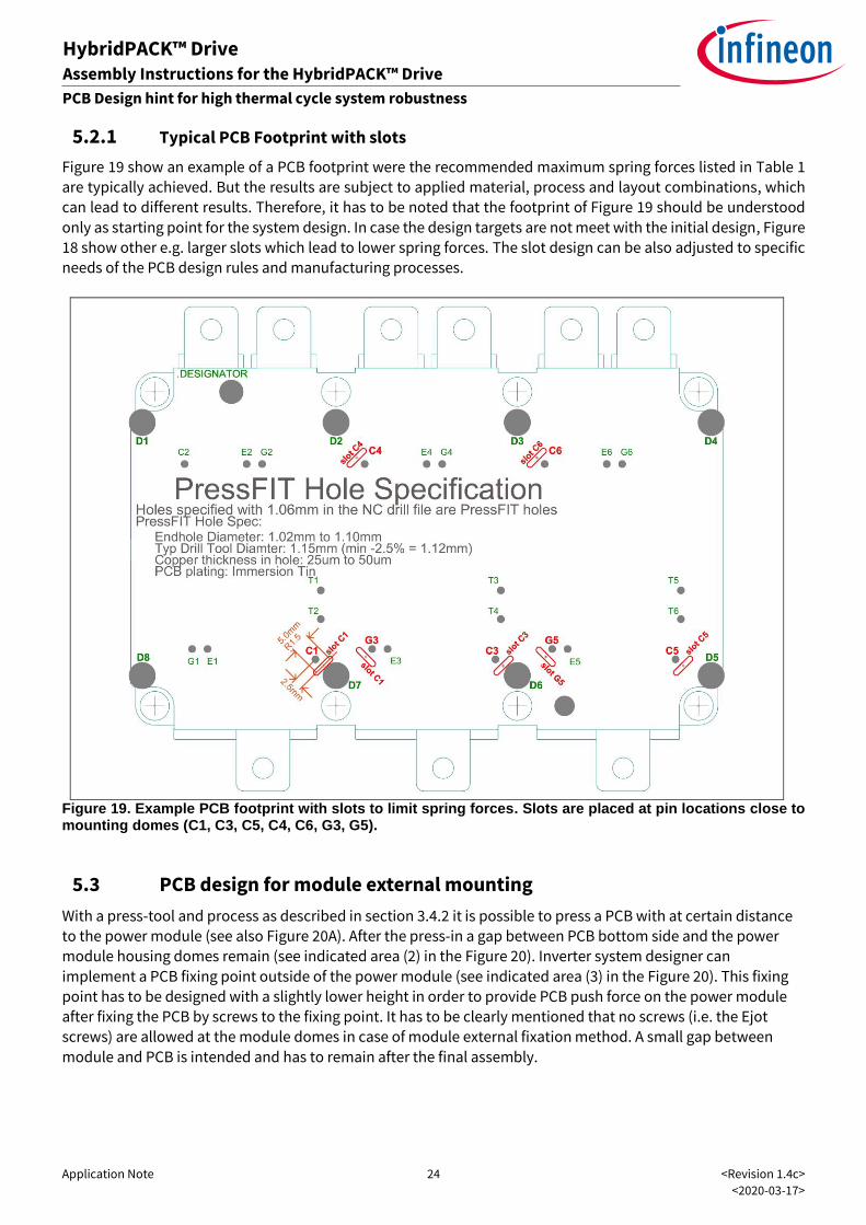
5.2.1 Typical PCB Footprint with slots
Figure 19 show an example of a PCB footprint were the recommended maximum spring forces listed in Table 1 are typically achieved. But the results are subject to applied material, process and layout combinations, which can lead to different results. Therefore, it has to be noted that the footprint of Figure 19 should be understood
only as starting point for the system design. In case the design targets are not meet with the initial design, Figure 18 show other e.g. larger slots which lead to lower spring forces. The slot design can be also adjusted to specific
needs of the PCB design rules and manufacturing processes.
Figure 19. Example PCB footprint with slots to limit spring forces. Slots are placed at pin locations close to mounting domes (C1, C3, C5, C4, C6, G3, G5).
5.3 PCB design for module external mounting
With a press-tool and process as described in section 3.4.2 it is possible to press a PCB with at certain distance
to the power module (see also Figure 20A). After the press-in a gap between PCB bottom side and the power module housing domes remain (see indicated area (2) in the Figure 20). Inverter system designer can
implement a PCB fixing point outside of the power module (see indicated area (3) in the Figure 20). This fixing point has to be designed with a slightly lower height in order to provide PCB push force on the power module after fixing the PCB by screws to the fixing point. It has to be clearly mentioned that no screws (i.e. the Ejot
screws) are allowed at the module domes in case of module external fixation method. A small gap between
module and PCB is intended and has to remain after the final assembly.

Application Note 25 <Revision 1.4c>
<2020-03-17>
HybridPACK™ Drive Assembly Instructions for the HybridPACK™ Drive
PCB Design hint for high thermal cycle system robustness
Figure 20 Example of distance press-in combined with module external mounted PCB. Distance keeper (1) ensure a certain distance of PCB to module dome (2). PCB can be fixed externally of the module (3).
Due to the larger distance of PCB fixing point to the pins it is a typical system behavior that spring forces of the
PCB are reduced in such way that design recommendation of Table 1 is fulfilled without slots in the PCB close to the signal pins.

Application Note 26 <Revision 1.4c>
<2020-03-17>
HybridPACK™ Drive Assembly Instructions for the HybridPACK™ Drive
Power Module Cooling System
6 Power Module Cooling System
The power losses occurring in the module must be dissipated in order to not exceed the maximum permissible operating temperature specified in the datasheet. Therefore, the design of cooling system/heat sink is of great importance.
HybridPACK™ Drive has a pin-fin array on the base plate, which makes liquid cooling very effective in sense of the thermal performance. The base plate is made of copper (Cu) material with nickel (Ni) plating. The pin fin structure is suitable for cooling fluids like water/ethylene glycol mixture.
PLEASE NOTE: During the mounting process, damage to the nickel plating or mechanical deformation of the pin fin structure as well as contamination, scratches or other damage in the sealing region (see Figure 24) must be strictly avoided.
6.1 Reference Cooler Design
The cooler design has a great impact on the overall cooling performance, which means the combination of
thermal resistance/impedance, pressure drop, and cooling flow rate. Thus, for all of these thermal related product specifications a reference cooling system is needed, where the given specification values are valid.
The reference cooler design for HybridPACK™ Drive with PinFin baseplate is shown in Figure 21.
The reference cooler design for HybridPACK™ Drive “Wave” with its Ribbon Bond Cooling Structure (e.g.
FS770R08A6P2B) is shown in Figure 22.
The HybridPACK™ Drive with Flat baseplate is not shown. These modules can be mounted to one of the reference coolers for the PinFin or the Ribbon Bond cooling structure in order to have a simple performance scaling option. Furthermore, the Flat baseplate can be mounted also on closed cooler
systems where heat transfer is conducted via thermal grease. For closed cooler systems a thermal grease
thickness of typical 70um has to be applied.

Application Note 27 <Revision 1.4c>
<2020-03-17>
HybridPACK™ Drive Assembly Instructions for the HybridPACK™ Drive
Power Module Cooling System
DIN ISO 13715; ISO 2768-mK; DIN EN ISO1302; AlMgSi0.5
Figure 21 Reference cooler design for HybridPACK™ Drive with PinFin Cooling Structure (e.g. FS820R08A6P2B).

Application Note 28 <Revision 1.4c>
<2020-03-17>
HybridPACK™ Drive Assembly Instructions for the HybridPACK™ Drive
Power Module Cooling System
DIN ISO 13715; ISO 2768-mK; DIN EN ISO1302; AlMgSi0.5
Figure 22 Reference cooler design for HybridPACK™ Drive “Wave” with its Ribbon Bond Cooling Structure (e.g. FS770R08A6P2B). Optional: In the marked areas “Ribbonbond free area” small barriers can be designed in the cooler to generate additional turbulence. Please note that pressure drop will be significantly increased for minor Rth reduction. The reference FS770 cooler (see also datasheet values) does not consider optional barriers and is designed with simply flat cooler bottom as shown in the picture.
Figure 23 Difference in the cooler design for PinFin and Ribbon Bond cooling structure as on overview.
The cooler can be designed differently if other tradeoffs of thermal resistance/impedance, pressure drop and
flow rates must be achieved. Therefore, the reference cooler should be regarded as a design example, where the values from the corresponding product specification can be achieved.
The following requirements must be considered when either the reference design or other designs are used.
Roughness of the cooler: ≤ RZ25 (DIN EN ISO 1302) in area of the sealing.
Cooler Flatness at the module area: ≤ 50 µm

Application Note 29 <Revision 1.4c>
<2020-03-17>
HybridPACK™ Drive Assembly Instructions for the HybridPACK™ Drive
Power Module Cooling System
Exceeding the requirements above may lead to damage of the power module.
The cooler material should be AlMgSi0.5 or other alternative which is compatible to copper baseplate with nickel plating and which can withstand the mechanical stress required from a specific customer application.
The holes for the x-pins are designed in the reference cooler with a high margin (i.e. 8 mm depth holes). When
necessary for the system design it is possible to reduce these holes to 6.0mm depth.
6.2 Recommendation for the sealing ring
The power module baseplate is designed with a flat region of 6.5 mm surrounding the entire pin fin area (see
Figure 24). Considering a 4 mm thick groove for the sealing ring and a positioning tolerance of the sealing area
and the alignment to the cooling system of better than ±1mm, is it convenient to achieve a proper sealing.
Figure 24 The sealing region with 6.5mm surrounding the pin fin area.
For initial evaluation and power module qualification tests where an assembly was required, a sample sealing
ring from Freudenberg Sealing Technologies part number 192944/192945 was used. This sealing ring was of
EDPM 70 material and had a specification shown in Figure 25. For easier assembly and even higher robustness margin, a double sealing ring can be applied (see Figure 25).

Application Note 30 <Revision 1.4c>
<2020-03-17>
HybridPACK™ Drive Assembly Instructions for the HybridPACK™ Drive
Power Module Cooling System
A)
standard sealing ring
double sealing ring
B)
Figure 25 Drawing of a EPDM 70 sample o-ring (A) and corresponding groove size in the cooler (B).
The company Shanghai Transtech Sealing Technology designed a derivate of this initial design with the article number: YA-15070-E7061. This sample design was also applied in monitoring qualification and release of new products in the HybridPACK Drive modules, where mounting on cooler system was required for the test.
This design has “assembly knobs” supporting an easier assembly process. These knobs can fix the sealing ring
after it is attached to the cooler grove and will avoid the risk of displacements during the module assembly process.
A)
B)
Figure 26 Drawing of sample sealing ring designed by Transtech with knobs supporting the assembly process (A). Corresponding groove size in the cooler (B).
The sealing ring is held in a groove, which must be designed in the cooling system. It should be noted that the sample sealing rings shown above lead to positive results in power module
qualification tests. Nevertheless, it is necessary to perform system qualification test (e.g. according to LV124) if final system design and assembly meets the project specific application needs.
PLEASE NOTE: Infineon does not recommend the usage of a silicon gasket or other sealing methods. The usage of sealing methods different then sealing ring can cause damage on HybridPACK™ Drive module.

Application Note 31 <Revision 1.4c>
<2020-03-17>
HybridPACK™ Drive Assembly Instructions for the HybridPACK™ Drive
Power Module Cooling System
6.3 Cooling fluid
A general recommendation for a specific cooling fluid cannot be provided, as the power module is only one single
part in the entire cooling system. Following items have to be considered at the system supplier to find appropriate coolant fluid:
Coolant fluid with its corrosion protection has to be compatible with the aluminium of the cooler material and the nickel overplated Cu module baseplate.
Also other parts in the coolant system has to be compatible to the fluid type (e.g. Zn screws and chrome parts are typically not allowed in the cooling system).
The fluid mixture has to provide enough anti-freeze for the application conditions. Freezing events of the fluid has to be strictly avoided. Freezing fluid will lead to plastic deformation of the power module
baseplate and may lead to fluid leakage and/or isolation failure consequently.
For power module tests at Infineon where cooling is required (e.g. thermal characterization, power cycling tests) typically BASF Glysantin™ G30™ with an organic-acid-technologie (OAT) silicate-free corrosion protection is applied. A known effect in combination with HybridPACK Drive “Wave” FS770R08A6P2xx is a chemical
reaction of the corrosion protection of the Glysantin™ G30™ with the aluminum coolant structure (see Figure
27). This is a known effect of this coolant type and had in the tests no influence on thermal performance or pressure drop.
Figure 27 Example of HybridPACK Drive Wave FS770R08A6P2xx after long time tests with G30™ fluid. The aluminum cooling structure may appear black after the test. The reaction of the organic corrosion protection is a known effect and has no negative influence on the thermal performance or aging of the module.

Application Note 32 <Revision 1.4c>
<2020-03-17>
HybridPACK™ Drive Assembly Instructions for the HybridPACK™ Drive
Screw types and processes
7 Screw types and processes
7.1 Baseplate Mounting Screws
The power module baseplate is designed to be fixed on the cooling system by means of M4 screws.
A standard screw M4x10 ISO 4762 (DIN 912 A2) with washer M4 ISO 7090 (DIN 125 A2) may be possible, depending on mechanical application constraints (e.g. vibration, max pressure test,…). Considering production complexity
and highest mechanical robustness, we recommend the following screw type to fix the baseplate to the AlMgSi0.5 cooler: Table 7 Recommended baseplate fixing screw M4x10 ISO 7380-2 A2 (TX)
No Description min. typ. max. Remarks
1 Mounting torque 1.8 Nm 2.0 Nm 2.2 Nm
2 Max mounting speed 400rpm
3 Effective length of screw in cooler 6mm AlMgSi0.5 cooler material. Typical M4x10 screws are used.
Figure 28 Picture of recommended screw type M4x10 ISO 7380-2 A2 (typical appearance). The correct type has -2 suffix to the ISO norm and is a screw with flattened round head (German: Linsen-Flanschkopfschraube). The recommended screw type is also available with a TX20 screw head: ISO 7380-2-A2-TX.
Table 8 List of suitable baseplate fixing screw types for HybridPACK™ Drive
Type Description Remarks
M4x10 ISO 4762 screw M4 ISO 7090 washer
Standard M4 screw and washer Due to production complexity/cost only for lab
testing recommended.
M4x10 ISO 7380-2 A2 M4 screw with integrated washer
M4x10 ISO 7380-2 A2 TX M4 screw with integrated washer
and TX20 screw head.
Recommended for low to
high volume production
EJOT ALtracs Plus WN5152 AP 40x12/10 Self-tapping screw (see section 7.1.1 for requirements)
Recommended for high volume production.

Application Note 33 <Revision 1.4c>
<2020-03-17>
HybridPACK™ Drive Assembly Instructions for the HybridPACK™ Drive
Screw types and processes
7.1.1 Alternative: self-tapping screws for baseplate mounting
Self-tapping screws are well known for use in plastic materials but are also available and established since several years for metal materials. The main advantages are the elimination of drilling and thread cutting as well as the corresponding cleaning processes. This can lead to significant cost reduction and process time reduction
for cooler manufacturing at high production volumes. Furthermore, such self-tapping screws are known to be extremely rugged during vibration stress
The following rules and recommendations are given for the screw type:
EJOT ALtracs Plus WN5152 AP 40x12/10
The baseplate fixing points in the cooler has to be adjusted as shown in the drawing of Figure 29. The self-tapping screw should not be used in standard M4 threads.
Figure 29 Picture of the self-tapping EJOT ALtracs Plus WN5152 AP 40x12/10. A typical torque and mounting force diagram as well as drawing of the required fixing holes in the cooler. The holes can be also drilled with a standard drill tool (3.7mm 0°).
Table 9 Alternative baseplate fixing screw EJOT ALtracs Plus WN5152 AP 40x12/10:
No Description min. typ. max. Remarks
1 Mounting torque Meff 1.6 Nm 1.8 Nm 2.0 Nm Approx. Mw=2 Nm torque is required for the self-tapping. This
torque is not effective for the mounting force Ft. Self-tapping force strongly depends on cooler
material.
2 Recommended mounting speed 400rpm 600rpm Lower than 200rpm is not recommended
3 Module Clamping/Fixation during
mounting
2 kN Self-tapping screws require single
step mounting and appropriate module clamping. See section 7.2
Further important notes to avoid burrs and flakes in the final system:
The fixing holes in the cooler must be blind holes no clearance holes.
Only one time mounting is feasible.

Application Note 34 <Revision 1.4c>
<2020-03-17>
HybridPACK™ Drive Assembly Instructions for the HybridPACK™ Drive
Screw types and processes
The geometry of the EJOT screw is designed such that the burrs and flakes are only generated at the bottom of the screw thread.
The screw self-tapping moment depends on the cooler (housing) material. Infineon recommends to perform
mounting experiments with final cooler material. In these experiments the screw torque should be recorded. The cooler material specific self-tapping torque can be observed from the recorded data as shown in the example
with the reference cooler made of AlMgSi0.5 material.
Figure 30 Recorded screw torque in CNC machined cooler from AlMgSi0.5 material. The self tapping torque was at several experiments was in average 2.0Nm. For this part a total screw torque of 3.8Nm would lead to an effective screw torque of the required Meff = 1.8Nm.

Application Note 35 <Revision 1.4c>
<2020-03-17>
HybridPACK™ Drive Assembly Instructions for the HybridPACK™ Drive
Screw types and processes
7.2 Fixation/clamping of the module during the baseplate screw process
It is required to fix properly the power module to the cooler during the screwing process in order to avoid tilting
of the module with a possible damage (i.e. plastic deformation of the baseplate).
Following methods are preferred for module fixation. Screw orders are listed in section 7.4:
1. Multi-Step Screw Mounting: Place screw number 1 & 2 and fix with lowest torque (this avoids only module tilting and will not to provide a high clamping force). Fix screw 3 to 8 with low torque (e.g. 0.4-0.6 Nm). Fix screws with final torque as specified.
2. Module Clamping: After the power module (with PCB) is placed onto the cooling system the module
should be clamped in z axis of the module with a total force of Fc = 2 kN to ensure that the sealing
ring is fully compressed during the screwing process. The clamping can be performed in the area where the PCB mounting domes are located (see Figure 31) or alternative 8x 2.3mm diameter stamps can be used to apply the force in the corresponding module housing screw holes. It is important that
the PCB is not further pushed down during the clamping. Please note that the described 1st fixing method with multi step screw mounting is not suitable for self-tapping screws. For self-tapping screws it is mandatory to use proper clamping which enables a single step screw
mounting.
Figure 31. Indicated area where module can be normally clamped/hold down to the cooling system during the baseplate screw process.

Application Note 36 <Revision 1.4c>
<2020-03-17>
HybridPACK™ Drive Assembly Instructions for the HybridPACK™ Drive
Screw types and processes
7.3 PCB mounting screws on the module housing
Please take note that fixing the PCB to the module with screws is recommended after the module is attached to
the cooling system. The module dome was designed for the following screw type:
EJOT Delta PT WN5451 30 x 10 (for 1.6mm PCB thickness)
The initial 1.5mm (approximately) of the mounting stand-off, which can be seen in the drawing, serve as guidance
and cannot take any force. The thread in the plastics will form itself by driving in the EJOT screws. It is important to have an appropriate minimum turn-in speed, which causes a self-heating of the screw in order to have a proper thread forming in the plastic housing without splitting and cracking. An electronically speed controlled screwdriver is the preferred aid for this purpose. Furthermore, a straight insertion of the screw into the stand-off must be observed during assembly.
a)
b)
Meff
FtMw
M
t
c)
Figure 32: Picture of EJOT Delta PT typical appearance (a), basic mounting torque diagram (b), cross-section drawing of PCB screw in module dome (c).
Table 10 PCB fixing screws EJOT Delta PT WN5451 30x10:
No Description Unit min. typ. max. Remarks
1 Mounting torque Meff
Meff + Mw (for 1.6mm PCB)
Nm 0.45 0.50
1.0
0.55 Mw ≈ 0.45..0.5 Nm torque is required for
the self-tapping of a 10mm screw length
and 1.6mm PCB thickness. This torque is
not effective for the mounting force Ft and
may change for different screw length and
PCB thickness.
2 Recommended mounting speed rpm 400 600 Lower than 200rpm is not recommended.
3 Screw length in the module dome (te)
mm 6 9 Typical screw length 10mm for 1.6mm
thick PCBs.

Application Note 37 <Revision 1.4c>
<2020-03-17>
HybridPACK™ Drive Assembly Instructions for the HybridPACK™ Drive
Screw types and processes
7.4 Screw Orders (Baseplate and PCB)
The screw order as shown in Figure 33 is very important in order to avoid damage on the part. Please see section
7.1 and 7.3 for specification of screw type and torque as well as required processes like module fixation/clamping during the baseplate screw process.
Baseplate fixing after module assembly into cooler PCB fixing after base plate screwing
baseplate screw order Position PCB screw order Position
1 B2 1 D2
2 B6 2 D6
3 B3 3 D3
4 B7 4 D7
5 B4 5 D4
6 B8 6 D8
7 B1 7 D1
8 B5 8 D5
Figure 33 Screw order for baseplate and PCB screws.

Application Note 38 <Revision 1.4c>
<2020-03-17>
HybridPACK™ Drive Assembly Instructions for the HybridPACK™ Drive
Connecting to the Power Terminals
8 Connecting to the Power Terminals
8.1 Mounting Options
The copper power tabs are tin-plated and are thus well suited for screw type connections including clinch
processes as well as welding processes. Several mounting options are suitable and some examples are illustrated in Figure 34 where the HybridPACK™
Drive is connected to a DC-link capacitor. It is possible to have the mounting order: screw – power tab – busbar – nut (Figure 34 Opt. 1), nut – power tab – busbar – screw (Figure 34 Opt. 2),
In the examples the busbar is always a single part/sheet, but also two or three busbar sheets are possible to be
mounted in the stack and thus it is also possible to have instead of the screw head/nut only busbars as a direct
interface to the power tabs: e.g. screw – busbar - power tab – busbar – nut.
Further beneficial mounting options are given by the use of self clinching nuts. Standard M4 self clinching nuts
can be used in mounting holes designed for M5 screws. Thus, a M4 self clinching nut can be pressed into the power tab hole and busbars can be connected with a M4 screw (preferred the same screw type as used for
mounting the baseplate to the cooling system). In case the mounting order is reversed it is possible to use a M5 self clinching nut in a busbar and to use a M5 screw on the power tab side as counterpart (i.e. mounting option 4
in Figure 34 and Table 11).
Opt. 1)
Opt. 2)
Opt. 3)
Opt. 4) Screw – power tab – busbar – sc nut
Figure 34 Examples of power tab connection options.
Table 11 Power tab mounting options and recommended screw torque
Mounting
Option
Screw/Nut type Mounting torque Remarks
min. typ. max.
1,2 M5 ISO 4762 screw (M5 ISO 7090 washer)
M5 ISO4032 nut
3.6 Nm 4.0 Nm 4.4 Nm low volume
production & lab
testing
1,2 M5 ISO 7380-2-A2-(TX) screw M5 ISO6923 nut
3.6 Nm 4.0 Nm 4.4 Nm low volume production & lab
testing
3 M4 ISO 7380-2-A2-(TX) M4 self-clinching nut
e.g. “TR-S-M4-1” PEM “S-M4-0ZI”
1.8 Nm 2.0 Nm 2.2 Nm Low to high volume production & lab
testing

Application Note 39 <Revision 1.4c>
<2020-03-17>
HybridPACK™ Drive Assembly Instructions for the HybridPACK™ Drive
Connecting to the Power Terminals
4 M5 or M4 ISO 7380-2-A2-(TX) screw M5 or M4 self-clinching nut in busbar/capacitor
(depending on busbar/capacitor design)
3.6 Nm 4.0 Nm 4.4 Nm Low to high volume production & lab testing
5 welding - - - high volume production
The screw types in table give only a rough overview. Different types may be possible with same mounting torque in case the base of head or the spot face are comparable to the given types and the busbar material is suitable for such mounting.
8.1.1 Additional Information for Welding Processes
The HybridPACK™ Drive power modules without an ‘B’ in the ending of the type designation (e.g.
FS820R08A6P2B) indicates a module frame, which has no mounting hole in the power tab. Examples of these module types can be seen in Figure 35 . These plain power tabs of these products can be connected by means of welding processes. The welding process with its specific parameters have to be evaluated by the customer. A general recommendation to the process type or parameters is not possible as it is also depending on the
companion material of the busbar and the available welding equipment at the customer. Studies of institutes give a comprehensive guide for the pre-selection of applicable welding process types and can be found e.g. at [1]
table 3.3 or [3].
Material property of the power tabs for selecting the welding process:
Copper Type: oxygen free copper type Plating: galvanic tin
Please note that the power module frame has to be limited to 150°C during the welding process.
A laser welding machine supplier, which has already successfully performed pre-tests on the HybridPACK Drive power tabs can be found under [4].
Module for welding. Short tabs. FS820R08A6P2
(no B at the end of type designation)
Mixed version (LM). DC side screws and AC side long tab for welding FS820R08A6P2LM.
Figure 35 HybridPACK Drive Modules suitable for welding.

Application Note 40 <Revision 1.4c>
<2020-03-17>
HybridPACK™ Drive Assembly Instructions for the HybridPACK™ Drive
Connecting to the Power Terminals
8.2 Forces on Power Tabs
The system mounting should be designed in a way that minimal force is applied on the power tabs of the power
module. The tested and allowed forces on the power tabs are given in Figure 36. The specified force shown on one single tab is allowed simultaneous at all power tabs.
Figure 36 Allowed forces on the power tabs.

Application Note 41 <Revision 1.4c>
<2020-03-17>
HybridPACK™ Drive Assembly Instructions for the HybridPACK™ Drive
System Assembly Clearance & Creepage Distances
9 System Assembly Clearance & Creepage Distances
The datasheet of the HybridPACK™ Drive specifies clearance & creepage distances of the product itself. It is obvious that external parts can modify these distances in the system and thus it is mandatory to check clearance and creepage distances of the entire final system assembly.
Figure 37 shows an example where the power terminals are connected with screws by means of a standard hexagonal nut.
Figure 37 HybridPACK™ Drive with a hex nut (ISO 4032) for the power tab connection. The clearance shown in the drawing is uncritical as it is higher than the minimum product clearance itself of 4.5mm.
Even considering a fixing tolerance of ±0.25mm the clearance distance shown above is higher than the minimum
clearance in the module product itself, which is 4.5mm according to the product datasheet.
Please note: The distance to the cooler, housing, (all external parts), must also be checked. For example, the distance from the hex nut to the cooler. This can be done only on system level. Appropriate keep out or covering
with isolating parts (plastic) can typically increase critical distances in the system design.

Application Note 42 <Revision 1.4c>
<2020-03-17>
HybridPACK™ Drive Assembly Instructions for the HybridPACK™ Drive
Phase Current Sensor Integration
10 Phase Current Sensor Integration
Figure 40 show mechanical features of the HybridPACK Drive which can be used for design of phase current sensor solutions. The features are shown exemplarily with the FS820R08A6P2LB product derivate (PinFin Baseplate, Frame with Long AC Tabs) but are same for HybridPACK Drive with other baseplate or frame options.
The shown elements can be applied also for other products in the HybridPACK Drive family.
Figure 38 Mechanical features of the HybridPACK™ Drive for design of phase current sensor solutions.
Sensors often uses the module baseplate screws for mounting, especially in the indicated areas with (X). It is
recommended to design the contact face (X) of the current sensor with a similar size as the recommended
baseplate screw head. Typically a 9mm contact face is chosen, which can withstand the allowed maximum
mounting torque of the baseplate screws.

Application Note 43 <Revision 1.4c>
<2020-03-17>
HybridPACK™ Drive Assembly Instructions for the HybridPACK™ Drive
Traceability, Data Matrix and Part Markings
11 Traceability, Data Matrix and Part Markings
Traceability of materials, equipment and processes is a must for key automotive components. Therefore, the HybridPACK™ Drive is produced at Infineon in a seamless traceability environment. Nevertheless, traceability must not be aborted after the modules are shipped to the customer and assembled into the inverters. In order
to reap the full benefit of a traceability chain, the unique module number (module ID) should be linked to the inverter ID at customer side. Figure 39 shows the module labels and where to find the DMX-code necessary for tracing the module-ID.
Figure 39 Picture of module labels (typical appearance). For a seamless traceability the DMX code which is the module ID (or alternative the type designation + date code + serial number) should be recorded and linked to the inverter ID.
The DMX code is readable with all professional data matrix code scanners compatible to the IEC24720 and
IEC16022 standard.
Engineers in the lab can also use free DMX code reader apps on their smartphones.
Android: QR Extreme, QR Droid, and many others supporting data matrix codes. iOS: i-nigma QR, and many others supporting data matrix codes

Application Note 44 <Revision 1.4c>
<2020-03-17>
HybridPACK™ Drive Assembly Instructions for the HybridPACK™ Drive
Technical Drawing
12 Technical Drawing
12.1 Basic Explanation Coordinate System
Figure 40 Technical drawing with global and local coordinate systems as utilized by the HybridPACK Drive.
The drawing of the HybridPACK Drive utilizes a global coordinate system, which is defined by the X-Pins and is
mainly used for pre-alignment. The position of all elements like signal pins, mounting domes, etc. are given in this global system and makes it simple for designing companion parts like the PCB, busbar and housing. Furthermore, important interfaces like mounting domes, signal pins are also defined in local coordinate systems,
where position tolerances can be defined more precise. With such a drawing, the companion parts will be typically designed with respect to the relative tolerances from
the corresponding local systems and the positioning of the companion part to the power module can be best
designed/checked in the common global coordinate systems.
Figure 43 show the basics of technical drawings with global and local coordinate systems. A coordinate system is here defined by three elements. The 1st element defines a surface (see Figure 43a). The position where the line of the 2nd element vertical crosses the surface of the 1st element defines the origin (see Figure 43b). A further line from the 3rd element to the origin defines the rotation of the final 3D Cartesian coordinate system (see Figure 43c).
An additional local coordinate system can be defined when one or more elements are shifted. In the example of Figure 43d, the 2nd element (B) is replaced by element (E). The result is a local coordinate system, which is linear transformed to the global system. These local systems enables a comprehensive way to define relative tolerances of e.g. pin positions, mounting domes, etc. .

Application Note 45 <Revision 1.4c>
<2020-03-17>
HybridPACK™ Drive Assembly Instructions for the HybridPACK™ Drive
Technical Drawing
12.2 Pin Position and Pin Gauge
For power modules which have in product specification a note as shown in Figure 41A, a pin gauge test is
implemented in the production line at Infineon. The specification of this pin gauge is shown in Figure 41B for pinning as implemented in FS660R08A6P2xx. For other signal pin pattern like for the SIC MOSFET modules the
positions of the signal holes are placed but hole size spec will remain same. At power module production the parts are tested if pin gauge can be applied to the module. A low force in module z-direction on the gauge are
allowed (typical up to 10..20N, which is uncritical for the module and its pins). When the pin gauge can be smoothly attached to the module the test is rated as PASS and can be seen as a test if customer can later smoothly assembly their PCBs on the power module.
The basic description of the test and pin gauge specification is placed only for information how these modules are tested at Infineon production. It is not needed at customer side to test power modules at incoming inspection
again.

Application Note 46 <Revision 1.4c>
<2020-03-17>
HybridPACK™ Drive Assembly Instructions for the HybridPACK™ Drive
Technical Drawing
A)
B)
Figure 41 Extract of datasheet regarding pin positions (A). Specification of Infineon pin gauge for power module production test (B). Hole pattern can be adjusted for other signal pinning with same hole size spec (e.g. SIC MOSFET Module)

Application Note 47 <Revision 1.4c>
<2020-03-17>
HybridPACK™ Drive Assembly Instructions for the HybridPACK™ Drive
Storage and Transport
13 Storage and Transport
During transport and storage of the modules, extreme forces through shock or vibration have to be avoided as well as extreme environmental influences.
Storage of the modules at the limits of the temperature specified in the datasheet is possible, but not recommended. The recommended storage conditions according to IEC60721-3-1, class 1K2 should be assured for the
recommended storage time of max. 2 years.
Max. air temperature: Tmaxair=+40°C
Min. air temperature: Tminair=+5°C
Max. relative humidity: 85%
Min. relative humidity: 5%
Condensation: not permissible
Precipitation: not permissible
Icing: not permissible
Pre-drying of the power module prior to the press-in process (as is recommended for molded discrete
components, such as microcontrollers, TO-cases etc.) is not required for the HybridPACK™ Drive power modules.

Application Note 48 <Revision 1.4c>
<2020-03-17>
HybridPACK™ Drive Assembly Instructions for the HybridPACK™ Drive
Power Module Appearance
14 Power Module Appearance
This chapter explains frequent questions about the typical power module appearance.
14.1 Pin Rotation
The position tolerance is an important value and ensures that a PCB designed according to the recommendations fits to the power module. The positions of the pins are clearly specified in the product datasheet.
The pin rotation is not fixed as the interface (PCB via) is totally symmetric. A pin rotation is clearly visible due to the asymmetric pin geometry (i.e. three contact pressfit pin). An example is shown in Figure 42, where the rotation is indicated. Typically about 45° pin rotations can be seen. Nevertheless, different angles may occur in
the final product and it is no reason for an objection and has no influence on the final contact quality.
Figure 42 Pins are not symmetrical (three contact pressfit pins) and thus a rotation angle is visible. Different angles may occur in final product but are uncritical for the contact quality and is no reason for an objection.
14.2 Module Lid to PCB Distance
The power module lid is also guided with the module x-pins. In the area of the x-pins the module lid is in contact
to the PCB even before it is pressed down. After final assembly this ensures that the lid has contact to the PCB
and thus avoids noise during typical application vibration profiles. The force of the lid to the PCB is low and uncritical for the PCB.
Figure 43 The module lid has contact to the PCB before it is pressed onto the power module. This ensures a contact after the PCB is assembled and avoids noise during vibration profiles.

Application Note 49 <Revision 1.4c>
<2020-03-17>
HybridPACK™ Drive Assembly Instructions for the HybridPACK™ Drive
Power Module Appearance
14.3 Power Tab Tin Plating
The power tabs are made of copper with a tin plating. The plating has the role to avoid visual discoloration and
oxidation of the copper between power module production and the mounting processes. After assembly, the tin plating has no function and the contact resistance is the same as an un-plated pure copper power tab. In order
to provide the maximum possible compatibility to various connecting techniques like screw type connections, clinching and welding, it is mandatory to make the plating as soft as possible. Due to the desired compatibility
and the required softness, visible scratches (see Figure 43a) and/or not completely over-plated edges due to the stamping process (see Figure 43b) are of logical consequence and is no reason for an objection as it does not influence the product performance or quality.
a)
b)
Figure 44 Typical appearance of the copper power tabs, which have a very soft tin plating and provides maximum compatibility to different mounting processes.
14.4 Baseplate Surface
A typical appearance of the baseplate surface is a so called “marbling” or “white spots” structure. This structure can be observed after the galvanic nickel and its cleaning process of the baseplates. The roughness of the
baseplate, the chemical structure as well as the thickness of the Ni layer is not different to baseplates where this structure is not visible by naked eye. Such an appearance as shown in the Figure 45 is a normal appearance and
is no reason for an objection as it does not influence the product performance or quality.
a)
b)
Figure 45 Typical appearance of power module baseplate surface with a “marbling” or “white spots” structure.

Application Note 50 <Revision 1.4c>
<2020-03-17>
HybridPACK™ Drive Assembly Instructions for the HybridPACK™ Drive
References and Revision History
15 References and Revision History
The referenced application notes can be found at http://www.infineon.com
[1] Copper Development Association, “Welding copper and copper alloys“, http://www.copper.org/publications/pub_list/pdf/a1050.pdf
[2] Harting Technology Group, http://www.harting.com
[3] Deutsches Kupferinstitute, “Schweißen von Kupfer und Kupferlegierungen” http://copperalliance.de/docs/librariesprovider3/i012-mit-info-deutsches-kupferinstitut-pdf
[4] Trumpf Laser- und Systemtechnik GmbH, https://www.trumpf.com
[5] Alpitronic GmbH, http://www.alpitronic.it
Revision History
Date Version Changed By Change Description
2015-02 0.9
Tomas Reiter (IFAG ATV HP EDT AE) Christoph Koch (IFAG ATV HP PD)
Initial DRAFT Version.
2015-11 0.91 T. Reiter, C.
Koch
Revised:
- Updated template and typer corrections.
- PCB reflow note added 3.1.
- Revised hole spec for pressfit holes (for early prototype modules with date code before 1549 it is recommended to use slightly larger holes typ
1.1mm) 3.1. - PCB mounting screws chapter revised 3.5.
- Cooler mounting holes added 4.2. - M4 baseplate mounting screws ISO norms added 4.3. - Power module appearance chapter added 9.
2016-04 1.0 T. Reiter, C. Koch
Revised:
- Baseplate fixing screw type with TX20 head added 4.3. - Revised part markings chapter 7. - Fig 5 description corrected.
- Updated pictures.
- Updated chapter 5 (power tab connecting).
- Removed NDA.
2016-11 1.1 T. Reiter, C.
Koch
Revised: - PCB X-Pin holes: added remark for plated, unplated holes.
- PCB fixing screw updated torque. - Technical drawing of sealing area added. - Remark for cooler X-pin hole depth added. - Added module fixation during baseplate screw process.
- Added chapter technical drawing explanation
2017-10 1.2 T. Reiter, C.
Koch
Revision: - Appnote valid for HPDrive Module family FSxxxRxxA6P2xx & FSxxxRxxA6T4xx.
- Added cooler design for FS770R08A6P2 - PCB maximum hole size for x-pins removed (optional feature).

Application Note 51 <Revision 1.4c>
<2020-03-17>
HybridPACK™ Drive Assembly Instructions for the HybridPACK™ Drive
References and Revision History
Revision History
Date Version Changed By Change Description
-PressFIT tool with wider tolerance, which provide worst case an uncritical push force on the signal pins. - Added information for self tapping baseplate fixing screws. - Added information for reading DMX code.
- Added chapter: Hints for Phase Current Sensor Integration - Minor revised wording.
2018-10 1.3 T. Reiter, C. Koch
Revisions: - Enlarged guiding holes in PCB for seamless assembly
- Optimized press tool (new drawing). - Maximum allowed press-in force. Explanation about press-in speed
- Recommended optimized press-in stop criteria - Reference cooler for FS770R08A6P2xx adjusted to fit for final parts.
2019-05 1.4 T. Reiter
Revisions:
- revised document chapter structure incl. minor revisions in wording and updated pictures in entire document. - added new chapter for soldering modules.
- added new chapter PCB design hints for high thermal cycle robustness - added new section cooling fluid, within chapter power module cooling
system. - added new section pin position and pin gauge in chapter technical
drawing
2019-09 1.4b T. Reiter
Revisions: Technical content not changed from revision 1.4.
List of power modules incl order number in scope of this appnote added
(see section 1.1).
Broken document cross-references corrected
2020-03 1.4c T. Reiter
Revisions: Technical content regarding assembly not changed from revision 1.4.
Added section and pictures for typical appearance of module baseplate. Gauge drawing corrected to match calibration specification of gauge.
Corrected typers.
.

Trademarks of Infineon Technologies AG AURIX™, C166™, CanPAK™, CIPOS™, CoolGaN™, CoolMOS™, CoolSET™, CoolSiC™, CORECONTROL™, CROSSAVE™, DAVE™, DI-POL™, DrBlade™, EasyPIM™, EconoBRIDGE™, EconoDUAL™, EconoPACK™, EconoPIM™, EiceDRIVER™, eupec™, FCOS™, HITFET™, HybridPACK™, Infineon™, ISOFACE™, IsoPACK™, i-Wafer™, MIPAQ™, ModSTACK™, my-d™, NovalithIC™, OmniTune™, OPTIGA™, OptiMOS™, ORIGA™, POWERCODE™, PRIMARION™, PrimePACK™, PrimeSTACK™, PROFET™, PRO-SIL™, RASIC™, REAL3™, ReverSave™, SatRIC™, SIEGET™, SIPMOS™, SmartLEWIS™, SOLID FLASH™, SPOC™, TEMPFET™, thinQ!™, TRENCHSTOP™, TriCore™. Trademarks updated August 2015
Other Trademarks All referenced product or service names and trademarks are the property of their respective owners. ifx1owners.
Edition <2020-03-17>
Published by
Infineon Technologies AG
81726 Munich, Germany
© 2020 Infineon Technologies AG.
All Rights Reserved.
Do you have a question about this
document?
Email: [email protected]
Document reference
AN-HPD-ASSEMBLY
IMPORTANT NOTICE The information contained in this application note is given as a hint for the implementation of the product only and shall in no event be regarded as a description or warranty of a certain functionality, condition or quality of the product. Before implementation of the product, the recipient of this application note must verify any function and other technical information given herein in the real application. Infineon Technologies hereby disclaims any and all warranties and liabilities of any kind (including without limitation warranties of non-infringement of intellectual property rights of any third party) with respect to any and all information given in this application note. The data contained in this document is exclusively intended for technically trained staff. It is the responsibility of customer’s technical departments to evaluate the suitability of the product for the intended application and the completeness of the product information given in this document with respect to such application.
For further information on the product, technology, delivery terms and conditions and prices please contact your nearest Infineon Technologies office (www.infineon.com).
WARNINGS Due to technical requirements products may contain dangerous substances. For information on the types in question please contact your nearest Infineon Technologies office. Except as otherwise explicitly approved by Infineon Technologies in a written document signed by authorized representatives of Infineon Technologies, Infineon Technologies’ products may not be used in any applications where a failure of the product or any consequences of the use thereof can reasonably be expected to result in personal injury.