Humidity control inside electronic enclosures: Developing ... · Marianne Burggraf for her help in...
118
Humidity control inside electronic enclosures: Developing design principles based on empirical understanding Salil Joshy PhD Thesis DTU Mechanical Engineering Department of Mechanical Engineering
Transcript of Humidity control inside electronic enclosures: Developing ... · Marianne Burggraf for her help in...

Humidity control inside electronic enclosures: Developing design principles based on empirical understanding Salil Joshy
PhD Thesis
DTU Mechanical EngineeringDepartment of Mechanical Engineering


Humidity controlinside electronic enclosures:
Developing design principlesbased on empirical understanding
PhD Thesisby
Salil Joshy
October 2018
Supervisors :Professor Rajan Ambat
Senior Researcher Morten Stendahl Jellesen
Section of Materials and surface engineering
Department of Mechanical Engineering
Technical university of Denmark (DTU)
Kgs. Lyngby 2800
Preface
This thesis is submitted in candidacy for a PhD degree from the Technical Univer-sity of Denmark. The work titled ”Humidity control inside electronic enclosures :Developing design principles based on empirical understanding” has been carriedout at the department of Mechanical Engineering, section of materials and surfaceengineering, under the supervision of Professor Rajan Ambat and Senior researcherMorten Stendahl Jellesen. The PhD project was supported by Innovation FundDenmark through the IN-SPE project (Innovation consortium for sustained perfor-mance of electronics). The duration of the PhD programme was January 2015 toOctober 2018.
ii

Acknowledgements
I would like to acknowledge my supervisors Rajan Ambat and Morten StendahlJellesen for their guidance, continuous support, and invaluable advice throughoutthe study. I appreciate their dedication to the project, the time spent for fruitfuldiscussions and the freedom given to me to explore different approaches.
IN-SPE member companies Danfoss A/S, Grundfos A/S, Vestas Wind SystemsA/S, and Eltek are acknowledged for the funding and overall support of the PhDprogram. Special thanks to Annemette Riis, Jens Peter Krog, John B. Jacobsen,Kirsten Stentoft-Hansen, Dorthe Johansen, Niels Martin Henriksen, Øystein Larsen,Willy Høydal for all the fruitful discussions and advice in connection with the PhDstudies.
I am thankful to my colleagues from the research group, the section of Materialsand Surface Engineering and the section of Manufacturing engineering. Thanks toMarianne Burggraf for her help in the lab and Lars Pedersen for help with the ex-perimental setups. Special thanks to Vadimas Verdingovas, Helene Conseil, KamilaPiotrowska, Zygimantas Staliulionis, Parizad Shojaee and Sankhya Mohanty fortheir help and contributions to the project.
I would also like to thank my family and friends for their support and encour-agement during the study.
iii

Abstract
This PhD work was supported by Innovation fund Denmark and was part of IN-SPE(Innovation consortium for sustained performance of electronics) project. The aimof this PhD work was to understand the humidity build-up inside electronic enclo-sures and study suitable humidity control methods to improve climatic reliability ofelectronics. In this regard, the main focus of the work was the effect of enclosuredesign and packaging related parameters on humidity build up and humidity control.
The use of electronic control units and devices in wide variety of applications andalso in different climatic regions has led to more and more humidity related failuresin electronics. Currently, the enclosure design for electronics are based on experi-ence gained over the years at major electronic manufacturers, rather than based onscientific knowledge. This work aims to contribute to the scientific understandingof humidity build up and humidity control techniques at enclosure level.
Chapter 1 introduces the background to humidity related reliability issues inelectronics. Also explained are the objectives of the current work and structure ofthis thesis. Chapter 2 reviews literature on water layer formation on printed circuitboard assemblies (PCBA), humidity related failures and mechanisms of humiditytransport into electronic enclosures. Chapter 3 reviews the methods currently usedto prevent humidity related failures and suitable humidity control techniques inelectronics. Chapter 4 summarises the materials and experimental methods used inthis work. Results of the PhD work were appended with this thesis as individualresearch papers in chapters 5, 7, 9 and as non-manuscript form in chapters 6 and 8.
Paper-1 studied forced condensation as a humidity control method in electronicapplications. The effect of enclosure related parameters like opening sizes, enclosurevolumes, cooler surface area and cooling temperature on relative humidity (RH) werestudied. Paper-2 studied the effect of enclosure related parameters like opening size,inter-PCB spacing, heat capacity and power dissipation on humidity accumulation,condensation and degradation of surface insulation resistance (SIR) in an electronicenclosure with parallel arrangement of PCBs. The work in chapter 6 was doneto answer fundamental questions on humidity transfer from warm to cold. Theparameters studied were warm temperature, cold temperature and connecting holesize. Chapter 8 studied humidity and temperature inside an electronic enclosurewith retained water.
The investigations have demonstrated humidity transfer from warm to cold andhave shown that preferential condensation based humidity control techniques weresuitable for electronic applications. By suitable sizing of various enclosure openingsand cooling temperature the RH inside the electronic enclosure can be reducedto prevent humidity related failures. Electronic enclosure related parameters likeopening size, PCB spacing and heat capacity were found to affect humidity relatedreliability of electronics.
iv

Paper-3 studied a methodology to predict humidity and contamination relatedfailures in common electronic circuits using experimental data of SIR. The method-ology was also used to identify more reliable circuit topologies.
v

Resume
Dette ph.d. arbejde blev støttet af Innovationsfonden og indgik i IN-SPE (Innova-tionskonsortium for palidelig elektronik). Formalet med dette ph.d. arbejde var atforsta opbygningen af fugt inde i kabinetter til elektronik og undersøge metoder tilstyring af fugt og derved opna øget palidelighed af elektronik. Fokus har været paeffekten af kabinetdesign og parametre relevante for fugt opbygning og fugt styring.
Brugen af elektronik i mange forskellige applikationer og ogsa under forskelligeklimatiske pavirkninger har ført til flere fugt relaterede fejl. Typisk er kabinet designtil elektronik baseret pa erfaringer hos elektronik producenter. Dette arbejde sigtermod at bidrage til den fundamentale forstaelse af fugt opbygning og luftfugtighed-skontrolteknikker.
Kapitel 1 introducerer baggrunden for fugtrelateret palidelighed af elektronik,samt malene med det nuværende arbejde og struktur af denne afhandling. Kapitel2 gennemgar litteratur om dannelse af vandlag pa printkort, fugtighedsrelaterede fejlog mekanismer for fugttransport i kabinetter til elektronik. Kapitel 3 gennemgar demetoder, der i øjeblikket bruges til at forhindre fugt relaterede fejl og passende fugtstyringsteknikker i elektronik. Kapitel 4 opsummerer de eksperimentelle metoder,der anvendes i dette arbejde.
Resultaterne af ph.d.-arbejdet er vedlagt denne opgave som individuelle forskn-ingspublikationer i kapitel 5, 7, 8 og desuden i kapitel 6 og 8.
Artikel 1 omhandler kondensation som en fugt kontrolmetode i elektronik. Ef-fekten af indkapslingsrelaterede parametre som abningsstørrelser, indkapslingsvol-umener, køligere overfladeareal og køletemperatur pa relativ fugtighed blev un-dersøgt. Artikel 2 undersøger effekten af indkapslingsrelaterede parametre somabningsstørrelse, printkort afstand, varmekapacitet og effekttab pa fugt akkumuler-ing, kondensering og effekten pa overfladeisoleringsmodstand i et elektronisk kabinetmed parallelt arrangerede printkort. Kapitel 6 beskriver fundamentale spørgsmal omfugt overførsel fra varme til kolde omrader. Effekten af temperatur og hul størrelseer undersøgt. Kapitel 8 undersøgte fugt og temperatur i et kabinet med vand pavæskeform.
Undersøgelserne demonstrerede mulig fugt overførsel fra varme til kolde omraderog derved at fugt styring kan bruges til elektronik applikationer. Ved passende di-mensionering af forskellige indkapslingsabninger og afkølingstemperatur kan fugten iindkapslingen reduceres og være med til at forhindre fugtighedsrelaterede fejl. Kabi-net relaterede parametre som abningsstørrelse, printkort afstand og varmekapacitetviste sig at pavirke den fugtrelaterede palidelighed af elektronik.
Artikel 3 undersøgte en metode til at forudse fugt- og forureningsrelaterede fejli elektroniske kredsløb ved brug af eksperimentelle data. Metoden blev ogsa brugttil at identificere mere palidelige kredsløb.
vi

List of abbreviations
ABS Acronitrile butadiene styreneAH Absolute humidityBET Brunauer-Emmett-TellerBGA Ball grid arrayCFD Computational fluid dynamicsCOP Coefficient of performanceDRH Deliquescence relative humidityECM Electrochemical migrationECU Electronic control unitEMI Electromagnetic interferenceHASL Hot air solder levellingHVAC Heating, ventilation, and air conditioningIGBT Insulated-gate bipolar transistorIP Ingress protectionIPC Association Connecting Electronics IndustriesMOSFET Metal-oxide-semiconductor field-effect transistorNFF No fault foundPC PolycarbonatePCB Printed circuit boardPCBA Printed circuit board assemblyQFN Quad flat no-leadRC Resistor-capacitorRH Relative humidityRTD Resistance temperature detectorSIR Surface insulation resistanceSST Solid state transformerTEC Thermoelectric coolerWOA Weak organic acid
vii

List of publications
The following articles constitute a part of the thesis
1. S. Joshy, R. Ambat, “Humidity control in electronic enclosures by forcedcondensation”, draft to be submitted
2. S. Joshy, R. Ambat, “Humidity accumulation and condensation in electronicenclosures”, submitted to Microelectronics Reliability.
3. S. Joshy, V. Verdingovas, M. S. Jellesen, R. Ambat, “Circuit analysis topredict humidity related failures in electronics - Methodology and recommen-dations”, Microelectronics Reliability, Vol. 93, pp. 81-88, Feb. 2019
The following articles have been published during the course of the PhD, but donot constitute a part of thesis.
Journal articles
1. V. Verdingovas, S. Joshy, M. S. Jellesen, R. Ambat, ”Analysis of surface in-sulation resistance related failures in electronics by circuit simulation,” CircuitWorld, Vol. 43, Issue 2, pp. 45–55, 2017.
Conference proceedings / oral presentations
1. S. Joshy, V. Verdingovas, M. Jellesen, R. Ambat, ”Simulation of electroniccircuit sensitivity towards humidity using electrochemical data on water layer”,17th Electronics Packaging Technology Conference (EPTC), pp. 1-5, 2015.
2. Z. Staliulionis, S. Joshy, M. Jabbari, S. Mohanty, R. Ambat and J. H. Hat-tel, “Analysis of moisture transport between connected enclosures under aforced thermal gradient,” 18th Electronics Packaging Technology Conference(EPTC), pp. 320–324, 2016.
3. S. Joshy, M. S. Jellesen, R. Ambat, ”Effect of interior geometry on localclimate inside an electronic device enclosure”, 16th IEEE Intersociety Confer-ence on Thermal and Thermomechanical Phenomena in Electronic Systems(ITherm), pp. 779-783, 2017.
4. S. Joshy, M. S. Jellesen, R. Ambat, “Reliability of electronics to humidity-related failures”, Book of Abstracts Sustain 2017, Technical University of Den-mark, 2017.
viii

5. S. Joshy, M. S. Jellesen, R. Ambat, “Effect of internal heating and packagingparameters on humidity profile and corrosion reliability inside an electronicenclosure”, 17th Nordic corrosion congress, 2018
ix

Contents
1 Introduction 11.1 Background . . . . . . . . . . . . . . . . . . . . . . . . . . . . . . . . 1
1.1.1 Humidity and contamination related failures . . . . . . . . . . 11.1.2 Humidity accumulation inside electronic enclosures . . . . . . 21.1.3 Humidity control techniques . . . . . . . . . . . . . . . . . . . 3
1.2 Objectives of the work . . . . . . . . . . . . . . . . . . . . . . . . . . 31.3 Structure of the thesis . . . . . . . . . . . . . . . . . . . . . . . . . . 4
2 Humidity accumulation and failures in Electronics 72.1 Climatic reliability of electronics . . . . . . . . . . . . . . . . . . . . . 72.2 Water layer formation on PCBA . . . . . . . . . . . . . . . . . . . . . 82.3 Contamination . . . . . . . . . . . . . . . . . . . . . . . . . . . . . . 8
2.3.1 Solder flux residues . . . . . . . . . . . . . . . . . . . . . . . . 92.3.2 Contamination from user environment . . . . . . . . . . . . . 10
2.4 Important humidity related failures . . . . . . . . . . . . . . . . . . . 102.4.1 Leakage currents/SIR degradation . . . . . . . . . . . . . . . . 102.4.2 Electrochemical migration . . . . . . . . . . . . . . . . . . . . 11
2.5 Humidity accumulation in electronic enclosures . . . . . . . . . . . . 112.5.1 Enclosures for electronics . . . . . . . . . . . . . . . . . . . . . 112.5.2 Quantification of humidity . . . . . . . . . . . . . . . . . . . . 122.5.3 Humidity transport into electronic enclosures . . . . . . . . . 14
3 Methods to prevent humidity failures in electronics 223.1 Conformal coatings . . . . . . . . . . . . . . . . . . . . . . . . . . . . 22
3.1.1 Conformal coating failures . . . . . . . . . . . . . . . . . . . . 233.2 Potting . . . . . . . . . . . . . . . . . . . . . . . . . . . . . . . . . . . 233.3 Desiccants . . . . . . . . . . . . . . . . . . . . . . . . . . . . . . . . . 233.4 Heating . . . . . . . . . . . . . . . . . . . . . . . . . . . . . . . . . . 24
3.4.1 Heat production for humidity control . . . . . . . . . . . . . . 243.5 Condensation . . . . . . . . . . . . . . . . . . . . . . . . . . . . . . . 25
3.5.1 Thermoelectric coolers . . . . . . . . . . . . . . . . . . . . . . 263.6 Humidity control . . . . . . . . . . . . . . . . . . . . . . . . . . . . . 26
4 Materials and methods 314.1 Materials in electronics . . . . . . . . . . . . . . . . . . . . . . . . . . 31
4.1.1 Hygroscopic contamination-Sodium chloride . . . . . . . . . . 314.1.2 SIR PCBs . . . . . . . . . . . . . . . . . . . . . . . . . . . . . 314.1.3 Electronic enclosures . . . . . . . . . . . . . . . . . . . . . . . 32
4.2 Climatic testing . . . . . . . . . . . . . . . . . . . . . . . . . . . . . . 32
x

CONTENTS
4.3 Software packages used . . . . . . . . . . . . . . . . . . . . . . . . . . 324.4 Impedance measurements . . . . . . . . . . . . . . . . . . . . . . . . 33
5 Humidity control in electronic enclosures by forced condensation 345.1 Introduction . . . . . . . . . . . . . . . . . . . . . . . . . . . . . . . . 355.2 Materials and methods . . . . . . . . . . . . . . . . . . . . . . . . . . 365.3 Results . . . . . . . . . . . . . . . . . . . . . . . . . . . . . . . . . . . 37
5.3.1 Effect of cooling temperature . . . . . . . . . . . . . . . . . . 395.3.2 Effect of cold chamber opening . . . . . . . . . . . . . . . . . 415.3.3 Effect of connecting hole . . . . . . . . . . . . . . . . . . . . . 425.3.4 Effect of Warm chamber opening . . . . . . . . . . . . . . . . 445.3.5 Effect of opening sizes on transient times . . . . . . . . . . . . 445.3.6 Effects of cooler surface area and cold chamber volume . . . . 455.3.7 Discussion . . . . . . . . . . . . . . . . . . . . . . . . . . . . . 465.3.8 Conclusion . . . . . . . . . . . . . . . . . . . . . . . . . . . . . 48
5.4 Acknowledgement . . . . . . . . . . . . . . . . . . . . . . . . . . . . . 49
6 Humidity transfer from warm to cold 526.1 Materials and methods . . . . . . . . . . . . . . . . . . . . . . . . . . 526.2 Results . . . . . . . . . . . . . . . . . . . . . . . . . . . . . . . . . . . 54
6.2.1 Humidity profiles in the chambers . . . . . . . . . . . . . . . 546.2.2 Effect of chamber temperatures . . . . . . . . . . . . . . . . . 556.2.3 Effect of connecting hole size . . . . . . . . . . . . . . . . . . . 56
6.3 Conclusion . . . . . . . . . . . . . . . . . . . . . . . . . . . . . . . . . 57
7 Humidity accumulation and condensation in electronic enclosures 587.1 Introduction . . . . . . . . . . . . . . . . . . . . . . . . . . . . . . . . 597.2 Materials and methods . . . . . . . . . . . . . . . . . . . . . . . . . . 607.3 Results . . . . . . . . . . . . . . . . . . . . . . . . . . . . . . . . . . . 63
7.3.1 Effect of Power dissipation . . . . . . . . . . . . . . . . . . . . 657.3.2 Effect of separation . . . . . . . . . . . . . . . . . . . . . . . . 677.3.3 Effect of heat capacity . . . . . . . . . . . . . . . . . . . . . . 687.3.4 Opening size . . . . . . . . . . . . . . . . . . . . . . . . . . . . 71
7.4 Discussion . . . . . . . . . . . . . . . . . . . . . . . . . . . . . . . . . 727.5 Conclusion . . . . . . . . . . . . . . . . . . . . . . . . . . . . . . . . . 747.6 Acknowledgement . . . . . . . . . . . . . . . . . . . . . . . . . . . . . 75
8 Humidity profile inside electronic enclosures with retained water 798.1 Materials and methods . . . . . . . . . . . . . . . . . . . . . . . . . . 798.2 Results . . . . . . . . . . . . . . . . . . . . . . . . . . . . . . . . . . . 80
8.2.1 Effect of PCB separation . . . . . . . . . . . . . . . . . . . . . 808.2.2 Effect of hole size . . . . . . . . . . . . . . . . . . . . . . . . . 81
8.3 Conclusion . . . . . . . . . . . . . . . . . . . . . . . . . . . . . . . . . 81
9 Circuit analysis to predict humidity related failures in electronics- Methodology and recommendations 829.1 Introduction . . . . . . . . . . . . . . . . . . . . . . . . . . . . . . . . 839.2 Extraction of SIR data for circuit analysis from humidity experiments 849.3 Comparison of leak-current level from SIR and component testing . . 86
xi

CONTENTS
9.4 Analysis of humidity robustness of circuits using electrochemical data 879.4.1 Humidity robustness of differential amplifier circuit . . . . . . 889.4.2 Humidity robustness of Non-inverting comparator circuit . . . 899.4.3 Effect of contamination type on humidity robustness . . . . . 90
9.5 Improvements to circuit reliability due to humidity . . . . . . . . . . 929.5.1 Instrumentation amplifier vs differential amplifier . . . . . . . 929.5.2 Inverting comparator vs Non-inverting comparator circuit . . . 939.5.3 Higher humidity robustness by splitting high resistances . . . 93
9.6 Summary . . . . . . . . . . . . . . . . . . . . . . . . . . . . . . . . . 959.7 Acknowledgement . . . . . . . . . . . . . . . . . . . . . . . . . . . . . 95
10 Overall discussion 99
11 Overall conclusion 101
xii

Chapter 1
Introduction
1.1 Background
Electronic devices are used in different climatic conditions around the world. Someexamples are offshore wind turbines, solar microinverters, automobile electronic con-trol units (ECU), wearable electronics like smart watches, household appliances etc.Offshore wind turbines are exposed to high humidity and salt containing aerosols.Electronics used in photovoltaic applications are exposed to varying intensity of radi-ation from the sun, humidity etc. Automobiles use a wide variety of ECUs for enginecontrol, power steering, anti-lock braking, electronic braking distribution, stabilitycontrol to name a few. Some of these ECUs are in the controlled climate of thepassenger compartment, but, others are exposed to uncontrolled ambient climate.Wearable devices like smart watches and health monitoring gadgets are exposed tocorrosive sweat from the human body.
The 2008 Paris climate agreement envisages limiting the rise in average globalatmospheric temperature to less than 2oC. This has resulted in a drive towardsrenewable energy production like solar, wind, tidal etc in favour of coal and otherfossil fuel based energy power plants. The generated unregulated power from theserenewable sources needs to be processed and fed to the existing power grids. Theemissions from automobiles are also being reduced globally through legislation. Thishas led the automobile industry from internal combustion engine based propulsion tohybrid-electric and fully electric power trains. All these entail more wide spread useof electronics in power production, power transmission, and transportation segmentsin the future. An example of this is the solid-state transformer (SST) conceptfor power transmission. An SST can provide voltage regulation, reactive powercompensation, dc-sourced renewable integration and communication capabilities inaddition to the traditional step-up/step-down functionality of a transformer[1].
1.1.1 Humidity and contamination related failures
Figure 1.1 shows the different sources for failures in electronics[2]. Humidity andcontamination related failures make up 25% of failures in electronics[2][3]. Highhumidity can cause formation of water layer on printed circuit board assembly(PCBA) due to deliquescence or condensation. Presence of the water layer leadsto failures like high leakage currents and short-circuits due to electro chemical mi-gration (ECM)[4][5][6][7]. Failures and faults in electronics due to humidity can be
1

CHAPTER 1. INTRODUCTION
temporary or permanent. The temporary nature of faults can be due to the waterlayer evaporating away or a short-circuiting dendrite being vaporised due to thehigh current flowing through it. These transient failures lead to occurrence of nofault found (NFF) failure in electronic equipment[8]. The permanent failures are theresult of corrosion processes under way. Presence of hygroscopic contamination onPCBA increases the risk of humidity related failures by reducing the critical relativehumidity (RH) at which water layer is formed. The main sources of contaminationon PCBA are PCB manufacturing, component assembly process and atmosphericparticulates.
Figure 1.1: Source of failures in electronics (Wang et al., 2013 [2])
1.1.2 Humidity accumulation inside electronic enclosures
Electronics is usually placed in an enclosure to protect from ambient climate, atmo-spheric particulate contamination, for better heat transfer to the ambient, shield-ing from electromagnetic interference (EMI) etc. Electronic enclosures can preventingress of liquid water or entry of particulate matter to a certain extent by useof diffusion plugs[9]. But, diffusion plugs allow free movement of humidity betweenambient and enclosure. An electronic enclosure with openings can delay, but, cannotfully prevent ingress of humidity from the ambient by mass transport mechanismslike diffusion and convection[10][11][12]. Prevention of humidity ingress from theambient is possible only with hermetically sealed enclosures, which are not practi-cal since, openings are required on an enclosure for connection of external wiringharness, pressure equalisation with ambient and as drain holes for condensed wa-ter accumulated inside the enclosure. Humidity can also accumulate by diffusionthrough the walls of a polymer enclosure. High humidity can result from the releaseof absorbed and adsorbed humidity from the walls of an enclosure. So, a passiveelectronic enclosure cannot always protect the electronics from high humidity con-ditions. This necessitates use of humidity control techniques in electronic enclosuresto prevent humidity related failures.
2

CHAPTER 1. INTRODUCTION
1.1.3 Humidity control techniques
The most widely used method to protect electronics from high humidity is to coatthe surface of PCBA with a conformal coating. A conformal coating prevents waterlayer formation on PCBA surface by acting as a barrier between humid air andPCBA. But, the effectiveness of conformal coating as a method to prevent humidityrelated failures decreases in the presence of ionic residue from no-clean solder fluxesused in component assembly process. Also, conformal coatings show failures likeblistering, delamination, bubbles, pinholes and cracking under cycling temperaturesand pressures.
Another technique to prevent high humidity inside electronic enclosures is bythe use of desiccants. Desiccants have been used for humidity control in heating,ventilation, and air conditioning (HVAC) applications[13][14]. When the desiccantbecomes saturated with adsorbed moisture, it either needs to be replaced or re-generated. Replacement is feasible only in repairable electronic systems where as,regeneration requires built-in mechanically actuated devices to expose the desiccantto ambient air. This severely limits the use of desiccants for humidity control inelectronic devices to just storage and shipping.
1.2 Objectives of the work
The main focus of this work is to experimentally study humidity control inside elec-tronic enclosures by forced condensation. Another focus of the work is to study theeffect of power dissipation and different geometric parameters of an electronic en-closure on humidity accumulation under cyclic ambient temperature. Feasibility ofinternal heating for humidity control was also investigated. The electronic enclosurewas modelled after a real electronic control unit with parallel PCB arrangement.This work also suggests a methodology to model performance of electronic circuitsunder different conditions of humidity and contamination. The simulation method-ology would help predict humidity related failures in electronics by using leakagecurrent data from standard SIR patterns. The following are the major investiga-tions done in this work:
• Effect of geometrical parameters like controlled opening sizes, enclosure vol-umes and cold surface temperature on steady state and transient characteris-tics of preferential condensation based humidity control.
• Effect of enclosure geometric parameters like inter-PCB spacing, heat capac-ity, controlled opening sizes on humidity accumulation under cycling ambienttemperature conditions and feasibility of utilising internal heating for humiditycontrol.
• Investigation of a simulation methodology to predict humidity related failuresunder different conditions of humidity and contamination.
3

CHAPTER 1. INTRODUCTION
1.3 Structure of the thesis
Figure 1.2 shows the overall structure of the thesis. Chapters 1, 2, 3 and 4 in-troduce the background, literature on the topics and materials and experimentalmethods. Chapter 5 is a study of humidity control by forced condensation. Chap-ter 6 studies the transfer of humidity from warm to cold using glass enclosures toanswer fundamental questions on using condensation for humidity control. Chapter7 investigates humidity accumulation in electronic enclosures due to cycling ambi-ent temperature and internal heating. Chapter 8 studies humidity and temperatureprofiles in an electronic enclosure with retained water inside. Chapter 9 introducesa simulation methodology to predict humidity failures in electronic circuits. Theoverall discussion and conclusions are presented in chapters 10 and 11.
Figure 1.2: Structure of the PhD thesis showing literature reviewed and differentinvestigations
4

Bibliography
[1] K. Mainali, A. Tripathi, S. Madhusoodhanan, A. Kadavelugu, D. Patel, S.Hazra, K. Hatua, S. Bhattacharya, ”A Transformerless Intelligent Power Sub-station: A three-phase SST enabled by a 15-kV SiC IGBT”, IEEE Power Elec-tronics Magazine, vol. 2, Issue 3, pp. 31-43, 2015.
[2] H. Wang, M. Liserre, F. Blaabjerg, ”Toward reliable power electronics: chal-lenges design tools and opportunities”, IEEE Ind. Electron. Mag., vol. 7, no. 2,pp. 17-26, 2013.
[3] C. Sintamarean, F. Blaabjerg, H. Wang, Y. Yang, ”Real field mission profileoriented design of a SiC-based PV-inverter application”, IEEE Transactions onIndustry Applications, Vol. 50, Issue 6, pp. 4082-4089, 2014
[4] D. Minzari, M. S. Jellesen, P. Moller and R. Ambat, ” On the electrochemicalmigration of tin in electronics,” Corrosion science, Vol. 53, Issue 10, pp. 3366–3379, 2011.
[5] D. Minzari, M.S. Jellesen, P.R. Møller et al., ”Electrochemical migration onelectronic chip resistors in chloride environments”, IEEE Trans. Device Mater.Reliab., vol. 9, no. 3, pp. 392-402, 2009.
[6] V. Verdingovas, M.S. Jellesen, R. Ambat, ”Influence of sodium chloride andweak organic acids (flux residues) on electrochemical migration of tin on surfacemount chip components”, Corrosion Engineering science and technology, vol.48, Issue 6, pp. 426-435, 2013.
[7] V. Verdingovas, M. S. Jellesen and R. Ambat, ”Solder Flux Residues andHumidity-Related Failures in Electronics: Relative Effects of Weak OrganicAcids Used in No-Clean Flux Systems,” Journal of Electronic Materials, Vol.44, Issue 4, pp. 1116–1127, 2015.
[8] J. Jones, J. Hayes, ”Investigation of the occurrence of no-faults-found in elec-tronics”, IEEE Transactions on Reliability, vol. 50, no. 3, pp. 289-292, 2001.
[9] M. Tencer, J-S. Moss, ”Humidity Management of Outdoor Electronic Equip-ment: Methods Pitfalls and Recommendations”, IEEE Trans. Components andPackaging Tech., vol. 25, no. 1, pp. 66-72, 2002.
[10] M. Tencer, ”Moisture Ingress into Non hermetic Enclosures and Packages.AQuasi-Steady State Model for Diffusion and Attenuation of Ambient HumidityVariations”, Electronic components and technology conference, pp. 196–209,1994.
5

BIBLIOGRAPHY
[11] H. Conseil-Gudla, Z. Staliulionis, M. S. Jellesen, M. Jabbari, J. H. Hattel,R. Ambat, ” Humidity build-up in electronic enclosures exposed to constantconditions,” IEEE transactions on components packaging and manufacturingtechnology, vol.7, Issue 3, pp. 412–423, 2017.
[12] H. Conseil, V. C. Gudla, M. S. Jellesen, R. Ambat, Humidity build-up in atypical electronic enclosure exposed to cycling conditions and effect on corrosionreliability, IEEE Transactions on Components, Packaging and ManufacturingTechnology, vol. 6, Issue 9, pp. 1379–1388, 2016.
[13] M. M. Rafique, P. Gandhidasan, H. M. S. Bahaidarah, ” Liquid desiccant ma-terials and dehumidifiers – A review,” Renewable and Sustainable Energy Re-views, Vol. 56, pp. 179–195, 2016.
[14] M. Sultan, I. I. El-Sharkawy, T. Miyazaki, B. B. Saha, S. Koyama, ” Anoverview of solid desiccant dehumidification and air conditioning systems,” Re-newable and Sustainable Energy Reviews, Vol. 46, pp. 16–29, 2015.
6

Chapter 2
Humidity accumulation andfailures in Electronics
2.1 Climatic reliability of electronics
Use of electronic products in uncontrolled application environments has led to fail-ures due to temperature and humidity. Failure or malfunction of an electronicequipment can lead to loss of property, loss of life, customer dissatisfaction and lossof brand value for the manufacturer. Wang et. al. [1] has shown that humidityand contamination related failures account for 25% of failures in power electronicsystems. Humidity and contamination related failures are the result of local elec-trochemical corrosion on PCBA surface. Electrochemical corrosion can occur onPCBA due to presence of a) metals/alloys b) potential bias and c) humid environ-ment. PCBA surface also has hygroscopic and ionic residues from the manufacturingand component assembly process. Hygroscopic nature of the contamination causesa thicker water layer to form on PCBA even at lower RH values. The ionic natureof the residues increases the conductivity of the water layer formed. This leads toincreased leakage currents and electrochemical migration (ECM)[2]. In this regard,cleanliness of PCBA and accumulation of high humidity in electronic enclosures be-come important aspects concerning reliability of electronic equipment during its lifetime. Figure 2.1 illustrates the factors causing electrochemical corrosion in electronicapplications.
Figure 2.1: Factors causing corrosion in electronics under humid conditions
7

CHAPTER 2. HUMIDITY ACCUMULATION AND FAILURES IN ELECTRONICS
This chapter reviews the literature on humidity related failures in electronicsand various factors that contribute to it. These include enhancement of water layerthickness due to the presence of contamination and different ways in which highhumidity accumulates in an electronic enclosure. Also discussed are the fundamen-tal mass transport mechanisms, which contribute to humidity accumulation anddifferent matrices for quantifying humidity.
2.2 Water layer formation on PCBA
A surface exposed to humid air develops a thin microscopic layer of water. Thenumber of monolayers of water present on a surface in the presence of humid air canbe calculated according to Brunauer-Emmett-Teller (BET) theory[3] by:
N =cx
(1 − x)(1 + (c− 1)x)(2.1)
where,
c = eE0−E
RT
and,
x =P
P0
is the relative humidity (RH).As observed from equation 2.1 the thickness of the water layer is dependent on
the RH of the ambient air, with the water layer thickness increasing with highervalues of RH. For α− aluminium surfaces the number of monolayers is one at 35%RH and five at 70% RH[4]. The conductivity of water layer increase with largernumber of monolayers[4]. The number of monolayers required for ionic conductivityleading to failure varies from three to ten in literature[5]. Water can condenseon surface of a PCBA when the temperature of the surface decreases below dewpoint temperature of the ambient air. Dew point temperature has been describedin section 2.5.2. A thicker water layer can also form on surface of PCBA due topresence of hygroscopic and ionic contamination. At lower RH values the surfaceinsulation resistance of PCBA remain high. When the RH exceeds deliquescence RH(DRH) of the contamination on the PCBA surface, a thin film of saturated solutiondevelops on the contamination particle[6]. Thus, a thicker water layer can form evenat lower RH values due to presence of hygroscopic contamination. The presence of aconductive water layer on PCBA surface decreases the surface insulation resistanceleading to unacceptable leakage currents.
2.3 Contamination
The main sources of contamination on PCBA are from PCB manufacturing, com-ponent assembly process and application environment[6]. The PCB manufacturingrelated contamination present on PCBA are curing agents, flame retardants, etch-ing chemicals etc. Human handling of the PCBA during production can result inchlorides, organic acids, oils etc being present on the PCBA[2]. Contaminationfrom application environment consist of dust, aerosols and other particulate matter
8

CHAPTER 2. HUMIDITY ACCUMULATION AND FAILURES IN ELECTRONICS
containing ionic and hygroscopic materials. Figure 2.2 shows the different sourcesof contamination on PCBA[6]. The most common cause of leakage currents andSIR reduction related faults in electronics is caused by solder flux residues fromcomponent assembly process on PCBA[6].
Figure 2.2: Source of contamination in electronics(Verdingovas, 2015 [6])
2.3.1 Solder flux residues
No-clean solder fluxes are widely used for soldering electronic components to PCB.It is assumed that no-clean solder fluxes decompose during the soldering process andleave behind minimal benign residues on the PCBA. But, it has been found thatsoldering with no-clean fluxes leave behind considerable amounts of residues[7][8].The main failure causing constituent of no-clean fluxes is the activator component ofthe flux which is commonly a weak organic acid (WOA). Many of these WOAs arehygroscopic and ionic in nature leading to water layer formation due to deliquescenceand subsequent reduction in SIR. Table 2.1 gives a list of commonly used WOAs insolder fluxes and their properties.
In reflow soldering process for surface mount components, the solder flux pasteis applied to the contact pads, components are temporarily attached and the en-tire assembly is introduced into a reflow oven. During this process the flux aroundcomponent pads will spread away and gets trapped under components like ball gridarrays (BGA), quad flat no-lead (QFN) and other surface-mount components. Theflux residues remain even after the reflow soldering process, which could lead tofailures over time[9]. For through hole components, flux is sprayed on the bottomside of the PCB where the solder-wave makes contact. The low surface tension ofthe liquid flux causes it to flow and get trapped in the space between bottom side
9

CHAPTER 2. HUMIDITY ACCUMULATION AND FAILURES IN ELECTRONICS
Table 2.1: Properties of WOAs in no-clean solder fluxes
WOA. DRH(%) Solubility(g/1Kg water)Adipic >98 1515oC
Succinic >98 83.525oC
Glutaric 83-89 140025oC
DL-Malic 75-84 144026oC
Palmitic - 0.00720oC
of PCB and pallet[8][9]. The area between pallet and bottom side of PCB expe-rience less temperature during preheating and wave soldering causing incompletedecomposition of the flux leading to presence of residues on PCBA[9].
2.3.2 Contamination from user environment
Contamination from user environment causing corrosion in electronics can be classi-fied as corrosive gases and particulate contamination. Corrosive gases like SOx, H2Setc can react with the metallisation on the PCB causing corrosion[10][11]. Minzariet. al. [10] has shown the formation of silver dendrites on silicone encapsulatedhybrid circuits in the presence of sulphurous gases. It is observed that permeationof sulphur gases and humidity through the silicone coating resulted in uniform cor-rosion, formation of Ag2S and migration of silver[10].
Particulate contamination found in atmosphere contain nitrate, sulphate, chlo-ride, ammonium etc[12]. They are hygroscopic and when deposited on PCBA, aidin water layer formation causing failures. Dust and aerosols get drawn into elec-tronic enclosures through openings in the enclosure and due to forced air convectioncooling. Tencer[13] describes the different mechanisms of deposition of aerosols inelectronics which include brownian diffusion, gravitational settling, thermophoresis,electrophoresis etc. When the RH inside the electronic enclosure increases beyondthe deliquescence RH of the particulate contamination deposited on PCBA, a con-ductive water layer is formed. Another important factor required for SIR degrada-tion on PCBA due to atmospheric particulates is connectivity, which is the bridgingfrom particle to particle[13].
2.4 Important humidity related failures
2.4.1 Leakage currents/SIR degradation
Leakage currents are unintended currents flowing between two nodes of an elec-tronic circuit on a PCBA. As related to humidity related failures, leakage currentsoccur because of a conducting water layer formation between two nodes as explainedin section 2.2. The flow of leakage currents can affect the normal functionality ofan electronic circuit leading to equipment malfunction or failure. A reduction ofSIR is the result of flow of leakage currents. Kinner[14] shows the different path-ways a leakage current could take on a PCBA in presence of water layer and ioniccontamination. Zou and Hunt[15] has studied methods to characterise conduction
10
CHAPTER 2. HUMIDITY ACCUMULATION AND FAILURES IN ELECTRONICS
mechanisms on a PCBA using a.c impedance. Under low RH conditions, the bulk ofthe SIR measured is due to the high resistivity of the substrate. But, under humidconditions and presence of ionic contamination a conducting water layer forms onthe surface of the substrate. The conducting water layer can form a parallel path ofhigher conductivity compared to the substrate. This leads to considerable leakagecurrents between two nodes of a circuit through the water layer compared to thesubstrate. The current is carried by ions in the water layer.
Leakage currents/SIR reduction on PCBA under humid conditions and presenceof contamination can be found in literature[16][17][18][19][20]. From literature, it canbe seen that solder flux residues are the most frequent cause for leakage currents/SIRdegradation. Use of surface insulation resistance (SIR) patterns is an electricalmethod to quantify contamination and predict the propensity for leakage currentson a PCBA [14][15]. A method to prevent considerable leakage current on PCBAis to have a cleaning step in the production process after component assembly toremove the no-clean solder flux residues.
2.4.2 Electrochemical migration
Electrochemical migration (ECM) occurs when the metal ions from the anode part ofthe micro-electrochemical cells formed on PCBA deposit themselves on the cathodeby transport through the conductive water layer in presence of a electric potentialdifference. The deposition of the positive metal ions causes a dendrite to growfrom cathode to anode, eventually causing a short circuit between the anode andcathode. The dendrite might disappear due to the heat generated by the shortcircuit current. ECM can happen in the presence of a thick water layer formeddue to deliquescence and condensation or in the presence of monolayers of watermolecules in humid conditions[21]. The ECM that happens commonly in electronicsapplications is due to formation of a thick water layer in condensing conditionsand presence of hygroscopic contamination. Minzari has studied ECM of tin inelectronic applications[22][23]. The solder fluxes used in electronic component playsan important role in ECM on PCBA[24][16][17].
2.5 Humidity accumulation in electronic enclo-
sures
2.5.1 Enclosures for electronics
The function of an electronic enclosure is to:
• Protect the electronics from aggressive ambient climate
• provide a suitable path for excess heat dissipated in the electronics to beremoved to the ambient
• shield the electronics from external electromagnetic interference (EMI)
• shield the EMI generated by the electronics, and
• aesthetic reasons.
11

CHAPTER 2. HUMIDITY ACCUMULATION AND FAILURES IN ELECTRONICS
Electronic enclosures come in all shapes and sizes. Enclosures are normallymade of aluminium or a polymeric material. Common polymer materials used tomake enclosures are Polycarbonate (PC), acronitrile butadiene styrene (ABS) etc.Aluminium enclosures are preferred in applications with higher heat dissipation dueto the high thermal conductivity of aluminium and also its lower cost compared tocopper. Enclosures could also be made of combination of metal and polymer withmetal parts serving to dissipate heat more efficiently to the ambient.
Figure 2.3 shows a typical parallel arrangement of aluminium plates simulatingPCBs inside an enclosure. In power electronic applications, higher power carryingcircuits could be located on a separate PCB called a ’power PCB’. The logic circuitscan be located on another PCB called a ’control or logic PCB’. This is done tominimise conducted emissions caused by high frequency switching power circuitsfrom interfering with the operation of the logic circuits.
Figure 2.3: Typical internal view of enclosures used in electronics
Figure 2.3 also shows openings in enclosures used in electronics. Openings inelectronic enclosures could be intentional or unintended openings. Openings in elec-tronics could be:
• To aid in forced convective transfer of heat from the electronics to ambient
• A path for retained liquid water to flow out of the enclosure
• Space between wires in an unsealed signal connector
• Cracks in the enclosure body
2.5.2 Quantification of humidity
Humidity is water vapour present in air. The amount of water vapour present inair can be expressed using various quantities like mass fraction, absolute humidity,
12

CHAPTER 2. HUMIDITY ACCUMULATION AND FAILURES IN ELECTRONICS
relative humidity, dew point temperature etc. The amount of water vapour presentin a volume of air ’V’ can be expressed using the ideal gas law :
Pv.V = m ·Rv · T (2.2)
where Pv is the partial pressure of water vapour in air, ’m’ is the mass of watervapour, Rv is the gas constant for water vapour and ’T’ is the absolute temperature.The following sections explain each of the methods of quantification.
Absolute humidity
Absolute humidity (AH) is the total mass of water vapour present in a unit volumeof air. AH is the value m/V in equation 2.2. The common units of AH are g/m3
and kg/m3. The amount of water vapour a volume of air can hold varies withthe temperature of the air. When a volume of humid air at a particular AH andtemperature is cooled, the excess water vapour starts to condense out in the formof liquid water. Absolute humidity can be calculated according to the approximateformula:
AH =2.16 × (RH/100) × 288.68 × (1.098 + T/100)8.02
273 + T(2.3)
where ’T’ is the temperature in degree Celsius and RH is the relative humidity aspercent. Figure 2.4 shows the maximum amount of AH air can hold at differenttemperatures.
0 1 0 2 0 3 0 4 0 5 0 6 0 7 0 8 0 9 00
1 0 0
2 0 0
3 0 0
4 0 0
5 0 0
6 0 0
Satur
ated A
H (g/m
3)
T e m p e r a t u r e ( C )
Figure 2.4: Variation of saturated AH with temperature
13

CHAPTER 2. HUMIDITY ACCUMULATION AND FAILURES IN ELECTRONICS
Relative humidity
Relative humidity(RH) is the fraction of partial pressure of water vapour of a volumeof air to its saturated vapour pressure at a given temperature. 100% RH signifiesthe air is saturated with water vapour. RH is expressed in percent as:
RH(%) =Pv
Pvsat
· 100 (2.4)
Dew point
Dew-point temperature is the temperature air should be cooled to raise its RH to100%. Dew-point temperature can be approximated using the Magnus formula[25]as :
Tdew =a · [ln(RH/100) + b·T
a+T]
b− [ln(RH/100) + b·Ta+T
](2.5)
where ’a’ is 243.12, ’b’ is 17.62, ’RH’ is the relative humidity in percent and ’T’ isthe temperature in celsius. The importance of dew-point temperature is that airwith a particular RH would condense on a surface having a temperature less thanor equal to the dew-point temperature of the air.
2.5.3 Humidity transport into electronic enclosures
Humidity can enter an electronic enclosure through intended or unintended openingsin the enclosure. Humidity accumulation occurs when the ambient AH is higherthan the AH inside the enclosure. The main transport modes for humidity betweenambient and the enclosure are:
• Diffusion - isothermal and non-isothermal
• Convection - forced and natural
Figure 2.5 depicts the different modes of humidity transfer between ambient andelectronic enclosures[26].
Figure 2.5: Moisture transport in an electronic enclosure (Jacobsen et al., 2014 [26])
14

CHAPTER 2. HUMIDITY ACCUMULATION AND FAILURES IN ELECTRONICS
Humidity can diffuse through intended or unintended openings and also throughpolymer walls of an enclosure. Forced and natural convection are used in electronicsfor cooling purposes, giving rise to exchange of humid air between the enclosureand ambient. Natural convection between the electronic enclosure and ambient alsooccurs due to ambient temperature and pressure changes.
At any time, an electronic enclosure could be exchanging humidity with sur-roundings under all combinations of humidity transport modes. Conseil et. al. de-tails humidity accumulation in electronic enclosures under conditions of diffusion[27]and convection[28] with the ambient. The following subsections introduce diffusionand convective modes of transport.
Diffusion
Diffusion is the process by which matter is transported from one part of a systemto another as a result of random molecular motions[29]. The net movement of aspecies is from a region of higher concentration to regions of lower concentration.The driving force behind diffusion is the gradient in concentration. For isotropicmaterials the rate of transfer of diffusing substance through unit area of a section isproportional to the concentration gradient measured normal to the section[29]. Fora one-dimension system this becomes:
F = −DδCδx
(2.6)
where, ’D’ is the diffusion constant of the material. Equation 2.12 is called the Fick’sfirst law of diffusion after Adolf Fick. Fick’s second law of diffusion relates the timedifferential of concentration at a location in space to differential of concentrationwith respect to position. For a one-dimensional system this becomes[29] :
δC
δt= D
δ2C
δx2(2.7)
Tencer[30] has shown that for an enclosure as in figure 2.6 with opening dimen-sions much larger than the enclosure wall thickness, isothermal diffusion of humiditycan be modelled mathematically like the charging of an electrical capacitor througha resistance.
Figure 2.6: Schematic of an electronic enclosure with an opening
15

CHAPTER 2. HUMIDITY ACCUMULATION AND FAILURES IN ELECTRONICS
The time constant for charging is given by:
τ =V L
AD(2.8)
where ’V’ is the volume of the enclosure, ’L’ is the thickness of the enclosure wall,’A’ is the area of the opening and ’D’ is the diffusion coefficient for water vapour inair, 0.24cm2/s. If volume ’V’ is considered as hygric capacitance then the equivalentresistance becomes :
R =L
AD(2.9)
Humidity can also diffuse into an electronic enclosure with no openings throughpolymer walls of the enclosure. This involves combined sorption of water moleculesby the polymer and diffusion. The dissolution of water vapour in a solvent can bedescribed by Henry’s law. Henry’s law states that the concentration of a dissolvedgas is proportional to the partial pressure of the gas in contact with the solution.
C = kp (2.10)
where, ’C’ is the concentration of the gas, ’k’ is the solubility coefficient and ’p’is the partial pressure of the gas. The diffusion coefficient can be combined with thesolubility coefficient to give permeability.
P = kD (2.11)
When including effect of solubility, Ficks first law becomes:
F = −P δpδx
(2.12)
where ’P’ is the permeability and ’p’ is the partial pressure of water vapour.
Convection
Convection is the transport of mass, heat or momentum along with the bulk mo-tion of a fluid. An example is transport of water vapour due to flow of humid air.Convection can be classified broadly as natural or forced. Natural convection occursdue to interaction of gravity with a fluid having a density gradient. The densitygradient could be because of a temperature gradient or a concentration gradient.Natural convection of air in electronic enclosures occur because of temperature gra-dient caused due to heat dissipation by electronic components. Forced convectionoccurs in electronic enclosures because of the operation of fans used for cooling.Convection results in exchange of humid air between the electronic enclosure andthe ambient. This could result in humidity accumulation inside the enclosure if theambient absolute humidity is higher than the humidity inside the enclosure.
Convective heat transfer is described by Newton’s law of cooling. For a verticalflat plate of area ’A’ and surface temperature Ts the heat transferred from the plateto the fluid around it is given by:
Q = hA(Ts − T∞) (2.13)
16
CHAPTER 2. HUMIDITY ACCUMULATION AND FAILURES IN ELECTRONICS
where T∞ is the temperature of the bulk fluid and ’h’ is the convective heat transfercoefficient. The non-dimensional convective heat transfer coefficient called Nusseltnumber is given by the formula:
Nu =hL
K(2.14)
where ’L’ is the length of the flat plate and ’K’ is the conductivity of the fluid aroundthe plate. The significance of the Nusselt number is that it is the factor by whichheat or mass transfer gets amplified compared to when the only transport mode isconduction or diffusion for heat or mass, respectively. Due to the similarities in thedifferential equations used for transport of heat and mass, equations 2.13 and 2.14can be used to describe mass transport also.
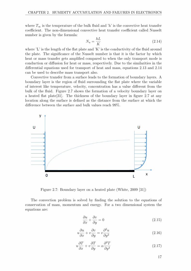
Convective transfer from a surface leads to the formation of boundary layers. Aboundary layer is the region of fluid surrounding the flat plate where the variableof interest like temperature, velocity, concentration has a value different from thebulk of the fluid. Figure 2.7 shows the formation of a velocity boundary layer ona heated flat plate[31]. The thickness of the boundary layer in figure 2.7 at anylocation along the surface is defined as the distance from the surface at which thedifference between the surface and bulk values reach 99%.
Figure 2.7: Boundary layer on a heated plate (White, 2009 [31])
The convection problem is solved by finding the solution to the equations ofconservation of mass, momentum and energy. For a two dimensional system theequations are:
∂u
∂x+∂v
∂y= 0 (2.15)
u∂u
∂x+ v
∂v
∂y= v
∂2u
∂y2(2.16)
u∂T
∂x+ v
∂T
∂y= α
∂2T
∂y2(2.17)
17

CHAPTER 2. HUMIDITY ACCUMULATION AND FAILURES IN ELECTRONICS
The equations 2.15, 2.16 and 2.17 are non-linear partial differential equationstherefore, solution to the above equations in a practical application need the use ofa computer.
18

Bibliography
[1] H. Wang, M. Liserre, F. Blaabjerg, ”Toward reliable power electronics: chal-lenges design tools and opportunities”, IEEE Ind. Electron. Mag., vol. 7, no. 2,pp. 17-26, 2013.
[2] R. Ambat, ”Perspectives on climatic reliability of electronic devices and com-ponents”, Imaps 2008, Rhode Island, USA, Nov. 2008.
[3] A. W. Adamson, A. P. Gast, Physical chemistry of surfaces, John wiley andsons Inc., 1997.
[4] B.-D. Yan, S.L. Meilink, G.W. Warren et al., ”Water adsorption and surfaceconductivity measurements on alpha-alumina substrates”, IEEE Trans. Com-pon. Hybrids Manuf. Technol., vol. 10, no. 2, pp. 247-251, 1987.
[5] M. Tencer, J-S. Moss, ”Humidity Management of Outdoor Electronic Equip-ment: Methods Pitfalls and Recommendations”, IEEE Trans. Components andPackaging Tech., vol. 25, no. 1, pp. 66-72, 2002.
[6] V. Verdingovas, ” Climatic reliability of electronics - Early prediction and con-trol of contamination and humidity effects”, PhD thesis, Technical universityof Denmark, Kgs. Lyngby, March 2015.
[7] M. S. Jellesen, D. Minzari, U. Rathinavelu, P. Moller and R. Ambat, ”Corrosionfailure due to flux residues in an electronic add-on device”, Engineering failureanalysis, vol. 17, Issue 6, pp. 1263-1272, 2010.
[8] H. Conseil-Gudla, M. S. Jellesen, R. Ambat, ” Contamination profile on typicalprinted circuit board assemblies vs soldering process,” Soldering and surfacemount technology, Vol. 26, Issue 4, pp. 194-202, 2014.
[9] P. Isaacs, T. Munson, ”What Makes No-Clean Flux Residue Benign”, SMTAPan Pacific Conference 2016 Proceedings.
[10] D. Minzari, M. S. Jellesen, P. Moller and R. Ambat, ”Morphological study ofsilver corrosion in highly aggressive sulfur environments,” Engineering failureanalysis, vol. 18, Issue 8, pp. 2126 – 2136, 2011.
[11] C. Hillman, J. Arnold, S. Binfield, and J. Seppi, “Silver and Sulfur: Case Stud-ies, Physics, and Possible Solutions,” SMTA International Conference, 2007.
[12] J. D. Sinclair, L. A. Psota-Kelty, C. J. Weschler and H. C. Shields, ” Depositionof Airborne Sulfate, Nitrate, and Chloride Salts as It Relates to Corrosion ofElectronics,” Journal of electrochemical society, Vol. 137, Issue 4, pp. 1200–1206, 1990.
19

BIBLIOGRAPHY
[13] M. Tencer, ”Deposition of aerosol (”hygroscopic dust”) on electronics – Mecha-nism and risk,” Microelectronics reliability, vol. 48, Issue 8, pp. 584–593, 2008.
[14] P. Kinner, ”The principle of surface insulation resistance (SIR) testing and itsrole in establishing the electrochemical reliability of a printed circuit board,”Proceedings of 2004 International Conference on the Business of ElectronicProduct Reliability and Liability, 2014.
[15] L. C. Zou; C. Hunt, ”Characterization of the Conduction Mechanisms in Ad-sorbed Electrolyte Layers on Electronic Boards Using AC Impedance,” Journalof the Electrochemical Society, Vol. 156, Issue 1, pp. C8–C15, 2009.
[16] V. Verdingovas, M. S. Jellesen and R. Ambat, ”Relative effect of solder fluxchemistry on the humidity related failures in electronics,” Soldering and SurfaceMount Technology, Vol. 27, Issue 4, pp. 146–156, 2015.
[17] V. Verdingovas, M. S. Jellesen and R. Ambat, ”Solder Flux Residues andHumidity-Related Failures in Electronics: Relative Effects of Weak OrganicAcids Used in No-Clean Flux Systems,” Journal of Electronic Materials, Vol.44, Issue 4, pp. 1116–1127, 2015.
[18] V. Verdingovas, M.S. Jellesen, R. Ambat, ”Influence of sodium chloride andweak organic acids (flux residues) on electrochemical migration of tin on surfacemount chip components”, Corrosion Engineering science and technology, vol.48, Issue 6, pp. 426-435, 2013.
[19] V. Verdingovas, M. S. Jellesen, and R. Ambat, ”Impact of NaCl Contaminationand Climatic Conditions on the Reliability of Printed Circuit Board Assem-blies”, IEEE Trans. Device Mater. Reliab., vol. 14, no. 1, pp. 42-51, 2014.
[20] J. E. Sohn, U. Ray, ”Weak organic acids and surface insulation resistance ”,Circuit world, vol. 21, Issue 4, pp. 22-26, 1995.
[21] S. J. Krumbein, ”Tutorial: Electrolytic models for metallic electromigrationfailure mechanisms”, IEEE Trans. Rel., vol. 44, no. 4, pp. 539-549, Dec. 1995.
[22] D. Minzari, ” Investigation of electronic corrosion mechanisms”, PhD thesis,Technical university of Denmark, Kgs. Lyngby, June 2010.
[23] D. Minzari, M. S. Jellesen, P. Moller and R. Ambat, ” On the electrochemicalmigration of tin in electronics,” Corrosion science, Vol. 53, Issue 10, pp. 3366–3379, 2011.
[24] D. Q. Yu, W. Jillek, E. Schmitt, ” Electrochemical migration of lead free solderjoints,” Corrosion science, Vol. 17, Issue 3, pp. 229–241, 2006.
[25] Sensirion, Application Note Dew-point calculation, pp.1-3, Available :http://irtfweb.ifa.hawaii.edu/˜tcs3/tcs3/Misc/Dewpoint Calculation HumiditySensor E.pdf [Accessed : 03-April-2019]
[26] J. B. Jacobsen, J. P. Krog, A. H. Holm, L. Rimestad, ”Climate-ProtectivePackaging: Using Basic Physics to Solve Climatic Challenges for Electronics inDemanding Applications”, IEEE Ind. Electron. Mag., vol. 8, no. 3, pp. 51-59,2014.
20

BIBLIOGRAPHY
[27] H. Conseil-Gudla, Z. Staliulionis, M. S. Jellesen, M. Jabbari, J. H. Hattel,R. Ambat, ” Humidity build-up in electronic enclosures exposed to constantconditions,” IEEE transactions on components packaging and manufacturingtechnology, vol.7, Issue 3, pp. 412–423, 2017.
[28] H. Conseil, V. C. Gudla, M. S. Jellesen, R. Ambat, Humidity build-up in atypical electronic enclosure exposed to cycling conditions and effect on corrosionreliability, IEEE Transactions on Components, Packaging and ManufacturingTechnology, vol. 6, Issue 9, pp. 1379–1388, 2016.
[29] J. Crank, ”The mathematics of diffusion”, Oxford university press, 1975.
[30] M. Tencer, Moisture Ingress into Non hermetic Enclosures and Packages.AQuasi-Steady State Model for Diffusion and Attenuation of Ambient Humid-ity Variations, Electronic components and technology conference, pp. 196–209,1994.
[31] F. M. White, ”Fluid Mechanics”, McGraw-Hill, 2009.
21

Chapter 3
Methods to prevent humidityfailures in electronics
This chapter reviews the methods to prevent SIR degradation and humidity relatedfailures. Broadly, one method to prevent humidity related failure is to increasethe intrinsic humidity robustness of the PCBA by proper design and cleanliness.Another method is to avoid contact with humidity or reduce the humidity levelin contact with the PCBA surface. Second method include reducing the humidityinside the electronic enclosure or by preventing the humidity from forming a waterlayer on PCBA surface by application of a barrier. The most widely used methodis by applying conformal coatings or by the use of potting material. Coatings andpotting provide protection by preventing humidity from forming a conductive waterlayer. Heating, desiccants, and forced condensation are humidity control techniques,which provide protection by reducing the humidity inside the electronic enclosure.Heating reduces RH inside the enclosure, where as desiccants and condensationreduces the absolute content of water vapour in the air inside the electronic enclosure.
3.1 Conformal coatings
Conformal coatings are thin layers of synthetic resins or plastics that are applied toPCBs and conform to the contours of the assembly[1]. Conformal coatings are usedin all types of electronics - automotive, industrial, military, aerospace and medicalwhere protection is required from engine fluids, chemicals, dust, abrasion, pressuri-sation/depressurisation, fluid/moisture resistance etc. According to the AssociationConnecting Electronics Industries (IPC), the functions of a conformal coating as re-gards to humidity are: to inhibit current leakage and short circuit due to humidityand contamination from service environment and inhibit corrosion[2]. Additionalfunctionalities include protection from physical abuse, such as handling, abrasion,temperature extremes, and radiation[3]. The common materials used for conformalcoatings are acrylics, epoxies and silicones. Conformal coating type is selected for anapplication based on its moisture absorption and permeation properties. The basicrequirement for a conformal coating acting as a barrier to moisture penetration isexcellent adhesion to the surface where it is applied. Lack of adhesion causes voidswhere moisture can permeate from the ambient causing water layer formation on thesurface in the voids. The adhesion to the surface depends on many factors like ma-terial properties of the coating, application process, wettability of the coating on the
22

CHAPTER 3. METHODS TO PREVENT HUMIDITY FAILURES INELECTRONICS
surface, presence of impurities on the surface etc. PCBA manufacturing process andcomponent assembly leaves behind hygroscopic and ionic contamination, which ifnot removed before application of a conformal coating can lead to improper adhesionwith PCBA. So, the use of conformal coatings requires a cleaning step in the pro-duction of PCBA. Other requirements for a conformal coating include low moisturevapour transmission rate, low out-gassing, low stress etc[3]. The desirable electricalproperties of a coating include high insulation resistance, high dielectric breakdownvoltage, low dielectric constant and dissipation factor. A standard used for testingthe performance, quality and consistency of a conformal coating is IPC-CC-830B[2].
3.1.1 Conformal coating failures
Good performance of a conformal coating requires the PCBA to be clean beforeapplying the coating. Presence of contamination under the coating leads to blis-tering, delamination, leakage currents and corrosion. Blistering can occur due toa mismatch in the surface energies of the coating and surface. Blistering can alsohappen if the coating allows humidity to permeate in to the interface between thesurface and the coating. Bubbles and pin holes occur in coatings due to prematuredrying, quick application of the coating and entrapment of air. Uneven thickness ofthe coating is another problem occurring due to capillary effects, gravity etc. Toothin coating leads to inadequate protection where as too thick a coating leads toproblems like bubbles, cracking and delamination. One of the main disadvantages ofusing conformal coating is that an extra cleaning step is required in the PCBA man-ufacturing process. Also, conformal coatings cannot be expected to work reliablyin ECUs subjected to high cycling temperatures and pressures due to delaminationand cracking of the coating.
3.2 Potting
In contrast to conformal coatings which were thin coatings of polymer applied tothe surface of a PCBA, potting involves filling the enclosed volume of PCBA with aspecial curable liquid compound. The liquid compound is allowed to solidify insidethe electronic enclosure, preventing exposure of the PCBA to moisture and corro-sive compounds. Common potting materials used are epoxy, polyurethane, siliconeetc[4]. Potting helps prevent failures due to humidity, contamination, corrosive gasesand also reduces effects of vibration on electronic components.
3.3 Desiccants
Desiccants are hygroscopic materials which can absorb water vapour from air thus,buffering the humidity levels inside an electronic enclosure. Use of desiccants is amethod of absolute humidity control, where the concentration of water vapour inthe air is controlled[5]. Solid and liquid desiccants are commonly used in HVAC aspart of dehumidifying the process air[6][7].
When a desiccant gets saturated, humidity absorption capability decreases. Asaturated desiccant has to be either replaced or regenerated. Regeneration is com-monly accomplished by heating the desiccant. Heating causes the desiccant to loose
23

CHAPTER 3. METHODS TO PREVENT HUMIDITY FAILURES INELECTRONICS
the adsorbed moisture to the ambient air due to higher vapour pressure generatedinside. When used for humidity control in electronics, desiccants need to be exposedto ambient air during regeneration by using mechanisms like a rotating desiccantbed. Other wise, the released humidity would condense on the PCBA. The pres-ence of moving components in desiccant based humidity control makes their useless attractive in most electronics applications. Desiccant based humidity controltechniques are suitable for electronics equipment, which undergo periodic repairor maintenance, where the saturated desiccant can be replaced. A good desiccantshould have large humidity storage capability and low regeneration temperature. Itshould also be non-volatile, non-corrosive and stable[6]. In electronics, desiccantsare widely used during storage and shipping. Common desiccants used in electronicsare silica gel, activated alumina, zeolite etc.
3.4 Heating
The principle of heating as a method of humidity control is to keep the electronicswarm enough so that the RH near the critical surfaces are below a certain safe limitsay, 60%. AHsat depends strongly on temperature and can be given by[5]
AHsat = const · exp(−EkT
) (3.1)
where ’E’ is the energy of evaporation, ’k’ is the Boltzmann constant, ’T’ isabsolute temperature and AH is expressed as concentration. As the temperature ofa parcel of humid air is increased, value of AHsat increases according to equation 3.1.Since RH is the ratio of AH to AHsat, RH decreases with increasing temperature.Therefore, humidity related failures in electronics can be prevented by maintainingthe RH inside an electronic enclosure below a safe limit by heating. Maximum valueof RH to prevent formation of a water layer (on a clean surface) thick enough forionic conductivity is 60%[5][8]. If the RH near PCBA surfaces can be maintainedbelow 60% by heating, humidity related failures can be prevented. The value of ∆Trequired to keep the RH below 60% is shown to be between 8 − 10oC[5]. However,the required humidity level can be higher depending on the cleanliness of the PCBAbased on the flux chemistry used for the soldering process and the residue level onthe board.
3.4.1 Heat production for humidity control
Heat to raise the temperature of PCBA surfaces can be generated by convective andradiative methods. In convective methods[9][10] the heat produced by a heatingelement is transported to the intended surface of PCBA by convection of warm air.In radiative heating, the heated element produces electromagnetic radiation whichwhen absorbed by a surface causes heating of the surface. Radiative heating eventhough used widely for heating of building interiors[11][12], it is still not practical tobe used for electronic applications due to the large size of the radiation producingelements.
Heat is also produced in an electronic unit by power dissipation from the elec-tronic components. The principal power dissipating components in electronics arepower resistors, inductors, transformers and semiconductors like diodes, metal oxide
24

CHAPTER 3. METHODS TO PREVENT HUMIDITY FAILURES INELECTRONICS
semiconductor field effect transistor (MOSFETS) and insulated gate bipolar tran-sistor (IGBT). In resistors, power dissipation occurs because of joule heating due tocurrent flow. In inductors and transformers heat is produced due to copper losses(joule heating) in the coils and core losses in the magnetic core due to fluctuations inthe magnetic field. Semiconductor devices like diodes, MOSFETs and IGBTs dissi-pate heat due to ohmic losses (joule heating) and also due to switching losses whenthe switches change states from ON to OFF and vice versa. The heat dissipated bythe electronic components could be preserved inside the electronic enclosure by suit-able insulation and used to keep the critical surfaces of the PCBA warm to preventhumidity related failures, depending on the application.
3.5 Condensation
Humidity in a volume of air can be reduced by condensing the water vapour in theair by forced condensation. Condensation occurs when a volume of humid air iscooled below its dew point temperature. The formula for dew point temperature isgiven by equation[13]:
Tdew =a · [ln(RH/100) + b·T
a+T]
b− [ln(RH/100) + b·Ta+T
](3.2)
where ’a’ is 243.12, ’b’ is 17.62, ’RH’ is the relative humidity in percent and ’T’ isthe temperature in celsius. The process of condensation is an exothermic processwith release of heat energy to the surface where condensation occurs. For water, theenthalpy of condensation is 40.66kJ/mol at normal pressure and 373oC.
There are two main types of condensation - film and dropwise condensation[14][15].In film condensation, the condensate wets the surface and forms a liquid film on thesurface that slides down under the influence of gravity. The thickness of the liquidfilm increases in the flow direction as more vapour condenses on the film. In drop-wise condensation, the condensed vapour forms droplets on the surface instead of acontinuous film, and the surface is covered by countless droplets of varying diameters[14]. Drop condensation is the most common type of condensation found in nature.Figure 3.1 shows the two main types of condensation.
Figure 3.1: Types of condensation on a surface ( Stephan, 1992 [15])
In film condensation, the heat released has to be transported from the surface ofthe liquid film through the liquid to the cold surface. The film of already condensedliquid acts as a resistance to heat transfer. In drop condensation, the condensed
25

CHAPTER 3. METHODS TO PREVENT HUMIDITY FAILURES INELECTRONICS
drops slide down under the influence of gravity, creating new locations for con-densation to happen. Hence, the heat transfer rates are much higher with dropcondensation than film condensation. Therefore, drop condensation is preferred tofilm condensation when higher condensing rates are required. Film condensationcan be described theoretically by Nusselt film condensation theory[15].
3.5.1 Thermoelectric coolers
Thermoelectric coolers(TECs) are well suited for forced condensation based dehu-midification in electronic enclosures. TECs work on the principle of peltier ef-fect. When a voltage difference is applied to a thermoelectric device a temper-ature difference is produced. Peltier effect has been applied for cooling[16][17],dehumidification[18][19], atmospheric water generation[20][21] etc.
A basic thermoelectric cooler (TEC) consists of a thermocouple, which consists ofa n-type and p-type semiconductor. A typical TEC consists of many thermocouplesconnected electrically in series and thermally in parallel to each other. The thermo-couples are sandwiched between thermally conducting plates. Figure 3.2 shows theconstruction of a TEC[22].
Figure 3.2: TEC construction (Wikipedia [22])
When d.c current is passed through the TEC, one side of the device is cooled andthe other side gets heated due to peltier effect. The amount of cooling achieved bythe cold side is proportional to the current passing through the TEC. The advantageof using TEC for cooling are lack of moving parts, reliability, small size, low noise,electrical control of cooling etc.
3.6 Humidity control
Control of humidity has been used widely in HVAC[23][24] and in special applicationslike museums, historic buildings and artefacts[25][26]. HVAC applications controlhumidity to improve the comfort of the occupants in houses, offices etc. Humiditycontrol in HVAC applications is commonly done by passing the process air over acooling coil to dehumidify the air. Cooling coils are operated normally by vapourcompression refrigeration systems. Hybrid systems which incorporate desiccants
26

CHAPTER 3. METHODS TO PREVENT HUMIDITY FAILURES INELECTRONICS
have shown to give better humidity control[27]. Use of desiccants in humidity controlalso need moving mechanisms like rotating desiccant beds for regeneration of thedesiccants[28][29]. All the above applications use considerable amount of energyfor their operation and also feature moving components which makes them lessattractive for electronic applications.
Kim et al. [30] has compared different humidity control techniques like heat-ing, fan, forced condensation and desiccants for a light emitting diode application.Forced condensation based humidity control was found to be the most suitable.Narayanaswamy[31] has studied the need for humidity control in subsea electrical en-closures and suggests heating and use of desiccants. The above mentioned literaturedoes not take into account factors like enclosure and packaging related parametersto optimise the humidity control process by heating or forced condensation.
TEC based forced condensation humidity control is used in HVAC[18][19], waterproduction[20][21] etc. In the above mentioned applications, the design is done todraw in as much air as possible into the enclosure using fans to increase the rateof dehumidification where as, forced condensation humidity control in electronicsshould work at comparatively low ingress rates through openings in the enclosure[5].Although many applications of condensation based dehumidification use a TEC,some special electronic applications like pumps for circulating cold water inherentlyprovide a cold and condensing surface which can be used for dehumidification bysuitably interfacing with the electronic enclosure[32][33].
27

Bibliography
[1] S. Zhan, M. H. Azarian, and M. G. Pecht,”Surface Insulation Resistance ofConformally Coated Printed Circuit Boards Processed With No-Clean Flux”,IEEE transactions on electronics packaging manufacturing, vol. 9, no. 3, pp.217–223, 2006.
[2] IPC-HDBK-830,”Guidelines for design, selection and application of conformalcoatings”, 2002.
[3] J. J. Licari, Coating Materials for Electronic Applications, 1st ed. Norwich,NY: Noyes Publications, 2003, pp. 2.
[4] electrolube.com, ’Resins for potting and encapsulation in the electronicsand electrical industries’, Available: https://www.electrolube.com/technical-articles/resins-for-potting-and-encapsulation/ [Accessed: 25-July-2018]
[5] M. Tencer, J-S. Moss, ”Humidity Management of Outdoor Electronic Equip-ment: Methods Pitfalls and Recommendations”, IEEE Trans. Components andPackaging Tech., vol. 25, no. 1, pp. 66-72, 2002.
[6] M. M. Rafique, P. Gandhidasan, H. M. S. Bahaidarah, ”Liquid desiccant mate-rials and dehumidifiers – A review”, Renewable and sustainable energy reviews,vol. 56, pp. 179-195, 2016.
[7] M. Sultan, I. I. El-Sharkawy, T. Miyazaki, B. B. Saha, S. Koyama, ” Anoverview of solid desiccant dehumidification and air conditioning systems,” Re-newable and Sustainable Energy Reviews, Vol. 46, pp. 16–29, 2015.
[8] M. Tencer, ”Moisture Ingress into Non hermetic Enclosures and Packages.AQuasi-Steady State Model for Diffusion and Attenuation of Ambient HumidityVariations”, Electronic components and technology conference, pp. 196–209,1994.
[9] I. Belov, J. Ryden, J. Lindeblom, Y. Zhang, T. Hansson, F. Bergner, and P.Leisner, ”Application of CFD Modelling for Energy Efficient Humidity Manage-ment of an Electronics Enclosure in Storage under Severe Climatic Conditions,”EuroSimE, p. 1-8, 21-23 April 2008.
[10] I. Belov, M. Lindgren, J. Ryden, Z. Alavizadeh, P. Leisner, ”CFD assisted de-sign evaluation and experimental verification of a logic controlled local PCBheater for humidity management in electronics enclosure,” 11th InternationalThermal, Mechanical and Multi-Physics Simulation, and Experiments in Mi-croelectronics and Microsystems (EuroSimE), 2010.
28

BIBLIOGRAPHY
[11] D. Anastaselos, I. Theodoridou, A. M. Papadopoulos, M. Hegger, ”Integratedevaluation of radiative heating systems for residential buildings”, Energy, vol.6, no. 7, pp. 4207-4215, July 2011.
[12] B. W. Olesen, ”Comparative Experimental Study of Performance of Radi-ant Floor-Heating Systems and a Wall Panel Heating System Under DynamicConditions”, Transactions-American society of heating refrigerating and air-conditioning engineers, vol. 100, no. 1, pp. 1011-1023, 1994.
[13] Sensirion, Application Note Dew-point calculation, pp.1-3, Available :http://irtfweb.ifa.hawaii.edu/˜tcs3/tcs3/Misc/Dewpoint Calculation HumiditySensor E.pdf [Accessed : 03-April-2019]
[14] Y. A. Cengel, A. J. Ghajar, ”Heat and Mass Transfer: Fundamentals andApplications”, McGraw-Hill, 2015.
[15] K. Stephan, ”Heat Transfer in condensation and boiling”, Springer-VerlagBerlin Heidelberg, 1992.
[16] B.J Huang, C.J. Chin, C.L. Duang, ”A design method of thermoelectric cooler”,International Journal of Refrigeration-revue Internationale Du Froid, vol. 23,no. 3, pp. 208-218, 2000.
[17] K. Chen, S.B. Gwilliam, ”An analysis of the heat transfer rate and efficiency ofTE (thermoelectric) cooling systems”, International Journal of energy research,vol. 20, no. 5, pp. 399-417, 1996.
[18] J.G. Vian, D. Astrain, M. Dominguez, ”Numerical modelling and a design of athermoelectric dehumidifier”, Applied thermal engineering, vol. 22, no. 4, pp.407-422, 2002.
[19] Y. Yao, Y. Sun, D. Sun, C. Sang, M. Sun, L. Shen, H. Chen, ”Optimizationdesign and experimental study of thermoelectric dehumidifier”, Applied thermalengineering, vol. 123, pp. 820-829, 2017.
[20] B. Gido, E. Friedler, D.M. Broday, ”Assessment of atmospheric moisture har-vesting by direct cooling”, Applied thermal engineering, vol. 182, pp. 156-162,2016.
[21] D. Milani, A. Abbas, A. Vassallo, M. Chiesa, D.A. Bakri, ”Evaluation of usingthermoelectric coolers in a dehumidification system to generate freshwater fromambient air”, Chemical engineering sciences, vol. 66, no. 12, pp. 2491-2501,2011.
[22] wikipedia.org, ’Thermoelectric cooling’, By michbich - own creation, CC BY3.0, Available: https://commons.wikimedia.org/w/index.php?curid=9076557[Accessed: 8-August-2018]
[23] V. Vakiloroaya, B. Samali, A. Fakhar, ”A review of different strategies forHVAC energy saving”, Energy conversion and management, Vol. 77, pp. 738-754, 2014
29

BIBLIOGRAPHY
[24] L. Z. Zhang, ”Energy performance of independent air dehumidification systemswith energy recovery measures”, Energy, Vol. 31, pp. 8-9, 2006
[25] C. Sease, ”The Development of the Humidity Control Module at Field Mu-seum”, Journal of the American institute for conservation, Vol. 30, Issue 2, pp.187-196, 1991.
[26] X. J. Zhang, C. V. Yu, S. Li, Y. M. Zheng, F. Xiao, ”A museum storeroomair-conditioning system employing the temperature and humidity independentcontrol device in the cooling coil”, Applied thermal engineering, Vol. 31, Issue17-18, pp. 3653-3657, 2011.
[27] P. Mazzei, F. Minichiello, D. Palma, ”HVAC dehumidification systems for ther-mal comfort: a critical review”, Applied thermal engineering, Vol. 25, issue 5-6,pp. 677-707, 2005
[28] G. Angrisani, A. Capozzoli, F. Minichiello, ”Desiccant wheel regenerated bythermal energy from a microcogenerator: Experimental assessment of the per-formances”, Applied energy, Vol. 88, issue 4, pp. 1354-1365, 2011
[29] P. Stabat, D. Marchio, ”Heat-and-mass transfers modelled for rotary desiccantdehumidifiers”, Applied energy, Vol. 85, issue 2-3, pp. 128-142, 2008
[30] C. S. Kim, J. G. Lee, J. H. Cho, D. Y. Kim, T. B. Seo, ”Experimental studyof humidity control methods in a light-emitting diode (LED) lighting device”,Journal of mechanical science and technology, Vol. 29, issue 6, pp. 2501-2508,2015
[31] V. Narayanaswamy, ”A review of thermal and humidity management needsand feasible solutions for next generation subsea electric systems”, Underwatertechnology, Vol. 32, issue 2, pp. 129-143, 2014
[32] grundfos.com, ’UPM3 OEM circulator pump for HVAC systems’, Available:https://www.grundfos.com/products/find-product/upm3.html#brochures.[Accessed: 19-July-2018]
[33] wilo.com, ’Wilo-Stratos PICO’, Available:http://productfinder.wilo.com/com/en/c00000016000391ce00020023/product.html#tab=3. [Accessed: 19-July-2018]
30

Chapter 4
Materials and methods
4.1 Materials in electronics
This sections describes the materials, test boards, enclosures and experimental meth-ods used for investigations presented in the appended papers. More detailed discus-sion on specific materials and methods for each investigation can be found in theappended papers.
4.1.1 Hygroscopic contamination-Sodium chloride
Sodium chloride at 15.6µg/cm2 was used as contamination in the investigation ofimpedance change during humidity accumulation in chapter. As per IPC J-STD-001D standard, the maximum allowable surface contamination level is 1.56µg/cm2
sodium chloride equivalent for soldered electrical and electronic assemblies. A tentimes higher contamination level was used for better sensitivity of the measurements.
4.1.2 SIR PCBs
The SIR PCBs used to study degradation of impedance due to humidity accumula-tion in chapter 7 is shown in figure 4.1. The FR-4 board was made in accordancewith IPC-4101/21. The thickness of the PCB was 1.6mm. The SIR pattern had ahot-air solder levelled (HASL) finish (Sn/Ag/Cu) solder alloy. The dimensions ofthe SIR pattern were 25mm x 13mm with a pitch distance of 0.3mm. The combpattern had 21 pairs of electrodes with an overlap of 10.8mm each.
31

CHAPTER 4. MATERIALS AND METHODS
Figure 4.1: SIR PCB used to study impedance degradation with humidity
4.1.3 Electronic enclosures
The enclosures used for the experiments in chapter 5 were made of polycarbonate.Each of the enclosures had dimensions of 170mm x 140mm x 95mm and thicknessof 3.3mm. The ingress protection (IP) rating of the enclosures was IP 66/67. Theexperimental set-up was made by joining two similar enclosures back to back.
The enclosures used for experiments described in chapter 7 were made of alu-minium. The external dimensions of the enclosure was 263mm x 162mm x 91mm.Thickness of the walls of the enclosure was 4mm. The enclosures had an ingressprotection rating of IP 66/67/68.
4.2 Climatic testing
The experimental works described in chapters 5 and 7 were conducted in controlledclimate inside an ESPEC SH-641 environment chamber. The operational range fortemperature and humidity were −40oCto150oC and 30% to 95% RH, respectively.The accuracy for temperature and humidity control were ±0.5oC and ±3.0% RH,respectively.
Temperature and humidity sensors were placed at different locations inside theenvironment chamber and enclosures. The temperature sensors used were PT1000type resistance temperature detectors (RTD) with an accuracy of ±0.6oC. Thehumidity sensors used were HIH 4021 from Honeywell with an accuracy of 3.5% RH.The sensed temperature and humidity were logged using Keithley Model 2700 dataacquisition system. The sampling rate of the data varied for different experimentsbut, the maximum sampling interval used was 2 min.
4.3 Software packages used
The circuit simulations in chapter 9 were done using Cadence Orcad Capture version16.6. The CFD simulations in chapter 5 were done using COMSOL Multiphysicsversion 5.3.
32

CHAPTER 4. MATERIALS AND METHODS
4.4 Impedance measurements
Impedance measurements of the contaminated SIR PCBs in chapters 7 and 8 weredone using a Biologic VSP series instrument. The impedance measurements weremade at a fixed frequency of 20KHz. The instrument had a 20V compliance voltagewith adjustable range (upper limits -20V and +20V). The current resolution of theinstrument was 760pA.
33

Chapter 5
Humidity control in electronicenclosures by forced condensation
Abstract
The purpose of this work is to study humidity control by forced condensation inelectronic enclosures. Humidity control using thermoelectric dehumidifiers has at-tracted lot of attention. There is no literature on application of condensation baseddehumidifiers for electronics applications. In this paper, a two-chamber design withwarm and cold chambers was used as a model system to investigate the condensa-tion effects. Both chambers were connected by an opening and a cooling elementwas placed in the cold chamber. The two chambers also had openings to the ambi-ent. The two-chamber setup helped to control outflow and ingress for each chamberseparately by changing the size of respective openings. The experimental setup alsosimulated a situation where the warm chamber was assumed to house electronicsand cold chamber contained a condensing surface. The size of chamber-to-chamber,chamber-to-ambient openings and cooling temperature are varied to study their ef-fects on RH inside both chambers. A computational fluid dynamics (CFD) modelof the experimental set-up was made and used to study the effect of cooler sur-face area and volume of the chambers on natural convection between the enclosuresand between enclosures and ambient. The RH inside the two chambers was foundto depend on the combination of openings used between the chambers and theirrespective openings to the ambient.
Keywords: Humidity, Electronic enclosure, Reliability, Condensation, Dehu-midification.
To be submitted as: S. Joshy, R. Ambat, “Humidity control in electronic enclosures
by forced condensation”.
34

CHAPTER 5. HUMIDITY CONTROL IN ELECTRONIC ENCLOSURES BYFORCED CONDENSATION
5.1 Introduction
The application of electronics in high humidity environments has made more fre-quent failures due to humidity. Electronics are used in high humidity environmentslike offshore wind turbines, wearable devices etc and uncontrolled environments likeautomobiles. Trend towards miniaturisation and development of high efficiency,low-power dissipating electronics has added to the complexity of the problem ofhumidity related failures in electronics. Advent of low RDS(on) and low switchingcharge MOSFETs based on SiC and GaN would reduce the overall heat dissipatedin power electronics, thus favouring lower temperatures and high humidity insidepower converters which use these technologies.
The main failure modes in electronics due to humidity are high leakage cur-rents and electrochemical migration(ECM)[1]. High humidity can result in elec-tronic enclosures due to diffusion, release of absorbed humidity from the walls ofthe enclosure[2] and under cycling conditions of ambient temperature and powerdissipation[3]. High humidity can condense to form liquid water on the printed cir-cuit board assembly (PCBA) when the temperature of the surface equals dew pointtemperature. Presence of ionic contamination from PCBA manufacturing processand atmospheric dust causes the water layer formed to be conductive leading toleakage currents and ECM. The residues on PCBA due to manufacturing processand atmospheric dust[4] could also be hygroscopic, leading to water layer forma-tion at RH significantly below the saturated level. No-clean fluxes commonly usedfor electronic component assembly contain weak-organic acids (WOA) as activatorswhich are hygroscopic and ionic[5].
The most commonly used technique to prevent humidity-related failures in elec-tronics is by application of a conformal coating. According to the Association Con-necting Electronics Industries (IPC), the functions of a conformal coating as regardsto humidity are: to inhibit current leakage and short circuit due to humidity andcontamination from service environment and inhibit corrosion[6]. There are vari-ous types of conformal coatings available in the market like acrylic, epoxy, silicone,polyurethane, paralyne etc. Literature shows that use of conformal coatings improvereliability if the level of contamination on PCB before coating is minimised [7]. Con-formal coatings prevent humidity-related failures by delaying the diffusive transportof water molecules to the PCB surface[7] and also by preventing the formation of aconductive water layer[8]. No-clean solder fluxes leave behind ionic contaminationwhich degrade the performance of conformal coatings [7][9]. Therefore, a cleaningstep is necessary in the PCBA manufacturing process to limit the degradation ofconformal coating performance.
Another way to prevent humidity-related problems in electronics is to keep therelative humidity (RH) inside the enclosure below a safe limit such as 60%. Indus-trial technologies for dehumidification can be broadly classified as desiccant basedand cooling based. In the former type, the excess humidity is removed by absorp-tion and adsorption into specific materials called desiccants. Desiccants could be inliquid [10] or solid [11] state as applied for heating, ventilation, and air-conditioningapplication. Desiccant based dehumidification systems need rotary devices to exposethe desiccants to process and regeneration air-streams alternatively. If desiccantsare used for humidity control in ECUs, it would require the use of rotating com-ponents which would lower the overall reliability of the electronic system, when
35

CHAPTER 5. HUMIDITY CONTROL IN ELECTRONIC ENCLOSURES BYFORCED CONDENSATION
the main intent was reliability improvement. Cooling can be achieved either byvapour-compression cycle or by thermoelectric coolers(TEC). TECs are particularlyadvantageous for electronic applications due to their direct use of electric power forcooling, small size, quite operation, lack of moving parts and low power consump-tion. TECs are employed for cooling of electronics, but there is a lack of literature onthe use of TEC based dehumidifiers for electronic applications. In certain specialisedapplications like motors with integrated drive electronics for pumping cold water,condensing surfaces are inherently present which can be utilised for dehumidificationof the electronics by connecting the electronic enclosure with the suitable surfacethrough openings. The two-chamber setup presented in this work also simulatesan application like a pump used to circulate cold water where motor electronics ishoused in a separate chamber compared to the impeller which pumps the water.
This study used a two chamber experimental setup to study condensation basedhumidity control in electronic enclosures. The chambers were connected to eachother and to ambient by openings. The two-chamber setup with openings helpedto achieve different transient mass transport rates for water vapour into and out ofeach chamber controlled by the size of the respective opening, thus enabling to studythe effect of opening sizes on humidity profiles inside an electronic enclosure. Thetwo-chamber setup also helped to isolate the net flows into and out of each chamberto specific openings. The cold chamber was assumed to house the condensing surfaceand warm chamber, the electronics. The size of the openings on the chambers wasvaried to study their effect on RH inside both chambers. Effect of cooling elementtemperature on RH inside both the chambers was studied. A CFD model of the twochamber setup was made and a parametric study of cooler surface area and chambervolumes were performed. The RH inside the chambers was observed to depend onthe combination of opening sizes used.
5.2 Materials and methods
The two-chamber setup consists of two polycarbonate enclosures of dimensions170mm X 140mm X 95mm connected back to back. Each of the enclosures areIP 66/67 rated. Openings were made on the common wall of the enclosures andalso to the ambient. Figure 5.1 and 5.2 shows a block diagram and picture of thetwo-chamber experimental setup.
The experimental setup was placed inside an ESPEC SH-641 environment cham-ber. The chamber RH and temperature were 97% and 25oC respectively. The coldchamber had a metal surface of circular cross section through which cold water wascirculated. This cold surface was the condensing and dehumidifying element. Coldwater at 10oC was circulated using a thermostat. A pair of temperature and RHsensors were placed in air at the centre of each chamber. The temperature sen-sors used were of PT1000 type resistive temperature sensors. The RH sensor usedwas HIH-4021 made by Honeywell. The data from the sensors were logged using aKeithley 2700 data acquisition system.
The experimental setup was allowed to equilibrate in RH and temperature tothe environment chamber climate. The experiment starts when the RH inside thechambers reach 90% and water at 10oC was circulated through the metal plate insidethe cold chamber. The RH inside the cold and warm chambers reduced until steadystate conditions are achieved. The experiment was done for different values of the
36

CHAPTER 5. HUMIDITY CONTROL IN ELECTRONIC ENCLOSURES BYFORCED CONDENSATION
Figure 5.1: Block diagram of the experimental set-up
Figure 5.2: Experimental set-up placed inside the climatic chamber with requiredsensor connections
openings and cooling temperature. The opening sizes used were 1mm, 2mm, 3mm,4mm, 5mm and 6mm. The cooling temperatures studied were such that the ambientdew-point temperature was always greater than the cold surface temperatures. Thisensured that condensation occurred on the cold plate. Table 5.1 gives the values ofcooling temperatures studied. COMSOL Multiphysics version 5.3 was used to makethe CFD model.
5.3 Results
Cooling of the cold plate results in natural convection inside the cold and warmchambers. Figure 5.3 shows a CFD simulation of velocity field and the directionsof flow of air through the openings of the chambers during steady state using a 2-D
37

CHAPTER 5. HUMIDITY CONTROL IN ELECTRONIC ENCLOSURES BYFORCED CONDENSATION
Table 5.1: Cooling temperatures studied
No. Cold water temperature(oC)1 2.52 53 7.54 105 12.56 15
model. The velocity profile is for a slice that passes through the centre of all thethree openings. It was observed that the net flow in the experimental set-up enteredthrough the warm chamber opening, then through the connecting hole to the coldchamber and exited through the cold chamber opening. Steady state concentrationsare achieved in the chambers when the net mass transfer of water vapour into andout of each of the chambers is zero.
Figure 5.3: Steady state air velocity inside the chambers in m/s
Figures 5.4 shows the typical RH, AH and temperature variations inside thechambers when cold water at 10oC was circulated inside the cooling plate. The pro-files in figure 5.4 are for a hole combination of 6mm each for warm chamber opening,connecting hole and cold chamber openings respectively. Due to the condensing con-ditions on the cold plate the AH and RH inside the cold chamber decreased belowthe ambient level to 14.5g/m3 and 66% respectively. The warm chamber also ex-perienced a delayed decrease in humidity to AH and RH values of 15.4g/m3 and65% respectively. The temperature inside the cold chamber measured by the sensordecreased by 2oC due to the effect of cold water circulation, but, the temperature
38

CHAPTER 5. HUMIDITY CONTROL IN ELECTRONIC ENCLOSURES BYFORCED CONDENSATION
inside the warm chamber remained the same as the ambient at 25oC. The tem-perature measured on the cooling plate was 15oC. The humidity profiles showed atransient time during which the humidity in both chambers decreased. A flat area inthe humidity profiles was observed when mass balance was achieved in both cham-bers. After this point, the humidity increased over time when the condensing platesurface area was saturated with water droplets. The humidity values presented inthe following sections correspond to the flat area of the humidity profiles.
0 . 0 0 . 2 0 . 4 0 . 6 0 . 8 1 . 04 0
5 0
6 0
7 0
8 0
9 0
1 0 0
1 1 0
1 2 0
RH (%
)
T I M E ( h r s )
W a r m c h a m b e r C o l d c h a m b e r
(a) RH profile
0 . 0 0 . 1 0 . 2 0 . 3 0 . 4 0 . 5 0 . 6 0 . 7 0 . 8 0 . 9 1 . 01 01 11 21 31 41 51 61 71 81 92 02 12 22 3
AH (g
/m3 )
T I M E ( h r s )
W a r m c h a m b e r C o l d c h a m b e r
(b) AH profile
0 . 0 0 . 2 0 . 4 0 . 6 0 . 8 1 . 01 21 41 61 82 02 22 42 62 83 0
Temp
eratur
e (C)
T I M E ( h r s )
W a r m c h a m b e r C o l d c h a m b e r C o o l i n g p l a t e
(c) Temperature profile
Figure 5.4: RH and AH inside the cold and warm chambers
It was also observed from figure 5.3 that there were two distinct flows observedin both chambers - humidity controlling flow which reduced the RH in each chamberand ingress of humidity whose effect was to increase the RH. In the warm cham-ber the humidity controlling flow was from the warm to cold chamber through theconnecting hole while the ingress was from the ambient through the warm cham-ber opening. In the cold chamber, the humidity controlling flow was from the bulkof the cold chamber volume to the cold plate. The humidity ingress into the coldchamber was both from ambient through the cold chamber opening and also fromwarm chamber through the connecting hole.
The following sections analyse the humidity profiles inside both chambers dueto the effects of warm chamber opening, connecting hole, cold chamber opening,cooling temperature, cooler area and the chamber volumes.
5.3.1 Effect of cooling temperature
The effect of cooling temperature on humidity profiles in warm and cold chambersis studied for a hole combination of warm chamber opening, connecting hole andcold chamber opening with a size of 6mm. Figure 5.5 shows the steady-state tem-peratures measured on the cold plate for the different values of circulated cold watertemperatures. The cold plate temperatures were higher than the circulated watertemperature due to heat loss to the air by convection.
39

CHAPTER 5. HUMIDITY CONTROL IN ELECTRONIC ENCLOSURES BYFORCED CONDENSATION
0 . 0 2 . 5 5 . 0 7 . 5 1 0 . 0 1 2 . 5 1 5 . 0 1 7 . 5 2 0 . 05 . 0
7 . 5
1 0 . 0
1 2 . 5
1 5 . 0
1 7 . 5
2 0 . 0
2 2 . 5
2 5 . 0
Cold
surfa
ce te
mpera
ture (
C)
C i r c u l a t e d w a t e r t e m p e r a t u r e ( C )
Figure 5.5: Measured cold surface temperature for different temperatures of circu-lated water
Figure 5.6 shows the results of CFD simulation for airflow from warm to coldchamber with different cold surface temperatures. The cold surface temperaturesused as input to the CFD simulation were the experimentally determined valuesshown in figure 5.5. When the temperature on the cold surface decreases, the naturalconvection flow from warm to cold chamber increased as shown in figure 5.6.
8 9 1 0 1 1 1 2 1 3 1 4 1 5 1 6 1 7 1 8 1 9 2 00
1 0 02 0 03 0 04 0 05 0 06 0 07 0 08 0 09 0 0
1 0 0 0
Volum
etric f
low (m
m3 /s)
C i r c u l a t e d w a t e r t e m p e r a t u r e ( C )
Figure 5.6: CFD simulation results of steady state volumetric flow of air from warmto cold chamber for different cold surface temperatures
Figure 5.7 shows the RH and AH inside the warm and cold chambers for differenttemperatures of circulated cold water.
40

CHAPTER 5. HUMIDITY CONTROL IN ELECTRONIC ENCLOSURES BYFORCED CONDENSATION
0 . 0 2 . 5 5 . 0 7 . 5 1 0 . 0 1 2 . 5 1 5 . 0 1 7 . 5 2 0 . 05 0
5 5
6 0
6 5
7 0
7 5
8 0
8 5
9 0 W a r m c h a m b e r C o l d c h a m b e r
RH (%
)
C i r c u l a t e d c o l d w a t e r t e m p e r a t u r e ( C )
(a) RH profile
0 . 0 2 . 5 5 . 0 7 . 5 1 0 . 0 1 2 . 5 1 5 . 0 1 7 . 5 2 0 . 01 11 21 31 41 51 61 71 81 92 02 1
W a r m c h a m b e r C o l d c h a m b e r
AH (g
/m3 )
C i r c u l a t e d c o l d w a t e r t e m p e r a t u r e ( C )
(b) AH profile
Figure 5.7: RH and AH inside the cold and warm chambers for different tempera-tures of circulated cold water
For a cold plate temperature of 9.4oC the RH in the cold and warm chamberswere 62.2% and 60% respectively. The RH in the cold chamber was higher than inthe warm chamber for this temperature. But, the AH in the warm chamber washigher than the cold chamber signifying transport of humidity from warm to coldchamber. The RH in the cold and warm chamber increased to 79.5% and 75.7%with increase in cold surface temperature from 9.4oC to 18.3oC. The RH in thecold and warm chambers showed a jump of 10% and 11.4% respectively for changein cold plate temperature of 15oC to 16.8oC. For other temperatures the change inRH in both chambers were much less.
5.3.2 Effect of cold chamber opening
The effect of cold chamber opening on humidity profile inside the chambers is stud-ied by varying the cold chamber opening diameter from 1mm to 6mm in intervalsof 1mm. The warm chamber opening and the connecting hole are fixed at 6mmdiameter. Figure 5.8 shows the experimentally measured RH and AH values.
It was observed from figure 5.8a that the RH in the cold chamber was 51.4%for 1mm diameter opening and it increased to 67.1% for 6mm diameter opening.Similar increase was found for cold chamber AH. The volumetric flow of air throughthe connecting hole for different cold chamber opening sizes is shown in figure 5.9.It was observed that humid airflow rates into cold chamber from the warm chamberincreased with higher cold chamber opening sizes. The increase in cold chamberhumidity with increasing opening size was due to the higher ingress of humidityfrom the warm chamber to cold chamber due to higher flow rates.
It was observed from figure 5.9 that the volumetric flow rate of air from the warmto cold chamber increases with larger diameter of the cold chamber opening. Sincethe warm chamber AH is higher than cold chamber AH, this flow from the warmchamber into the cold chamber contributes to increasing the AH in cold chamber.This also explained why the RH and AH in the warm chamber decreased withincreasing cold chamber opening diameters. For 1mm diameter opening on thecold chamber the volumetric flow from warm to cold chamber was almost negligibleat 1.38 mm3/s. This resulted in steady state RH in the warm chamber at 85%.
41

CHAPTER 5. HUMIDITY CONTROL IN ELECTRONIC ENCLOSURES BYFORCED CONDENSATION
0 1 2 3 4 5 6 75 0
5 5
6 0
6 5
7 0
7 5
8 0
8 5
9 0 W a r m c h a m b e r C o l d c h a m b e r
RH (%
)
C o l d c h a m b e r o p e n i n g ( m m )
(a) RH profile
0 1 2 3 4 5 6 7
1 2
1 4
1 6
1 8
2 0 W a r m c h a m b e r C o l d c h a m b e r
AH (g
/m3 )
C o l d c h a m b e r o p e n i n g ( m m )
(b) AH profile
Figure 5.8: RH and AH inside the cold and warm chambers for different cold chamberopenings
0 1 2 3 4 5 6 7
0
2 0 0
4 0 0
6 0 0
8 0 0
Volum
etric f
low ra
te (m
m3 /s)
C o l d c h a m b e r o p e n i n g ( m m )
Figure 5.9: Steady state volumetric flow of air from warm to cold chamber fordifferent sizes of cold chamber opening
With increase in the cold chamber opening diameter and higher volumetric flowthrough the connecting hole, the humidity in the warm chamber reduced due tomore humidity removal from warm to cold chamber. The steady state RH in thewarm chamber was found to be 61.5% for 6mm diameter cold chamber opening. Itwas also observed that the cold and warm chamber humidities did not vary for coldchamber opening sizes greater than 4mm.
5.3.3 Effect of connecting hole
The effect of connecting hole on humidity profile inside the chambers is studied byvarying the connecting hole diameter from 1mm to 6mm in intervals of 1mm. Thewarm chamber opening and the cold chamber opening are fixed at 6mm diameter.
42

CHAPTER 5. HUMIDITY CONTROL IN ELECTRONIC ENCLOSURES BYFORCED CONDENSATION
Figure 5.10 shows the experimentally measured RH and AH values.
0 1 2 3 4 5 6 75 0
5 5
6 0
6 5
7 0
7 5
8 0
8 5
9 0 W a r m c h a m b e r C o l d c h a m b e r
RH (%
)
C o n n e c t i n g h o l e ( m m )
(a) RH profile
0 1 2 3 4 5 6 7
1 2
1 4
1 6
1 8
2 0 W a r m c h a m b e r C o l d c h a m b e r
AH (g
/m3 )
C o n n e c t i n g h o l e ( m m )
(b) AH profile
Figure 5.10: RH and AH inside the cold and warm chambers for different sizes ofconnecting hole
Figure 5.11 shows the volumetric flow rate of air through the connecting hole atsteady state. It was observed that the flow rate shows an increase from 0.65mm3/sto 606mm3/s for a change in connecting hole diameter from 1mm to 6mm.
0 1 2 3 4 5 6 7
0
2 0 0
4 0 0
6 0 0
8 0 0
Volum
etric f
low ra
te (m
m3 /s)
C o n n e c t i n g h o l e ( m m )
Figure 5.11: Steady state volumetric flow of air from warm to cold chamber fordifferent sizes of connecting hole
It was observed from figure 5.10a that humidity inside the warm chamber didnot reduce much from the ambient RH for connecting hole size of 1mm, even thoughthe cold chamber RH is low at 52.6%. With increase in connecting hole size, thesteady state humidity in the warm chamber increased from 55.6% to 65% for holesize variation from 2mm to 6mm. The increase in connecting hole size from 1mmto 6mm also caused an increase in cold chamber RH from 52.6% to 66% as shownby figure 5.11.
43

CHAPTER 5. HUMIDITY CONTROL IN ELECTRONIC ENCLOSURES BYFORCED CONDENSATION
5.3.4 Effect of Warm chamber opening
To study the effect of warm chamber opening on the humidity profiles inside thechambers, the cold chamber opening and connecting hole sizes are kept fixed at 6mm.The warm chamber opening diameter is varied from 1mm to 6mm with intervals of1mm. Figure 5.12 shows the RH and AH profiles in the warm and cold chambersfor different diameterss of the warm chamber opening. It was observed that the RHand AH levels in both chambers increased with increasing size of the warm chamberopening.
0 1 2 3 4 5 6 75 05 25 45 65 86 06 26 46 66 87 0
W a r m c h a m b e r C o l d c h a m b e r
RH (%
)
W a r m c h a m b e r o p e n i n g ( m m )
(a) RH profile
0 1 2 3 4 5 6 71 1 . 01 1 . 51 2 . 01 2 . 51 3 . 01 3 . 51 4 . 01 4 . 51 5 . 01 5 . 51 6 . 01 6 . 51 7 . 0 W a r m c h a m b e r
C o l d c h a m b e r
AH (g
/m3 )
W a r m c h a m b e r o p e n i n g ( m m )
(b) AH profile
Figure 5.12: RH and AH inside the cold and warm chambers for different sizes ofwarm chamber opening
The warm chamber RH showed an increase from 55.6% to 66% where as the coldchamber RH increased from 53.5% to 66% for change in warm chamber opening from1mm to 6mm. It was also observed that humidity control still occurred in the warmchamber for warm chamber opening size of 1mm in contrast to the results withcold chamber opening and connecting hole of 1mm. The corresponding increasein volumetric flow rate from warm to cold chamber for change in warm chamberopening size from 1mm to 6mm was 1.23mm3/s to 606mm3/s as shown in figure5.13. In spite of this increase in volumetric flow from warm to cold chamber, thehumidity inside the warm chamber increased with higher warm chamber openingsize.
5.3.5 Effect of opening sizes on transient times
Transient time is defined as the time from the start of applying cooling to the instantwhen the RH inside the warm chamber approaches within 3.5% of the final steadystate value. Figures 5.14a, 5.14b and 5.14c show the transient times for humiditycontrol in the warm chamber for different sizes of cold chamber opening, connectinghole and warm chamber opening. It was observed that transient times reducedwith increasing opening sizes due to higher volumetric flow rates as shown beforein figures 5.9, 5.11 and 5.13. The lower values of transient times for cold chamberopening and connecting hole for 1mm opening size was due to absence of humiditycontrol for this opening size. Where as, for warm chamber opening size of 1mmshowed a transient time of 10hrs.
44

CHAPTER 5. HUMIDITY CONTROL IN ELECTRONIC ENCLOSURES BYFORCED CONDENSATION
0 1 2 3 4 5 6 7
0
2 0 0
4 0 0
6 0 0
8 0 0
Volum
etric f
low ra
te (m
m3 /s)
W a r m c h a m b e r o p e n i n g ( m m )
Figure 5.13: Steady state volumetric flow of air from warm to cold chamber fordifferent sizes of warm chamber opening
0 1 2 3 4 5 6 70 . 0
0 . 5
1 . 0
1 . 5
2 . 0
Trans
ient ti
me (h
rs)
C o l d c h a m b e r o p e n i n g ( m m )
(a) Transient time for coldchamber opening sizes
0 1 2 3 4 5 6 70 . 0
0 . 5
1 . 0
1 . 5
2 . 0
2 . 5
Trans
ient ti
me (h
rs)
C o n n e c t i n g h o l e ( m m )
(b) Transient time forconnecting hole sizes
0 1 2 3 4 5 6 7
0 . 0
2 . 5
5 . 0
7 . 5
1 0 . 0
1 2 . 5
Trans
ient ti
me (h
rs )
w a r m c h a m b e r o p e n i n g ( m m )
(c) Transient time forwarm chamber openingsizes
Figure 5.14: Transient time for RH inside warm chamber for different opening sizes
5.3.6 Effects of cooler surface area and cold chamber volume
A parametric study of steady state airflow velocity from the warm to cold chamberwas done to find the effect of cooling surface area and cold chamaber volume oncondensation humidity control. The cooling surface radius was varied from 10mmto 50mm. The cold chamber volume was varied by using different lengths of the coldchamber keeping other dimensions fixed. Figure 5.15a shows the effect of coolingsurface radius and figure 5.15b shows the effect of cold chamber volume on theairflow velocity from warm to cold chamber.
Figure 5.15a showed that airflow rate into the cold chamber increased with highercooler surface area. Also figure 5.15b showed that volumetric flow rate into the coldchamber increased for a smaller size. The results also suggest that a higher airflowvelocity into the cold chamber can be achieved not just by increasing the openingsizes but also by a higher condensing surface area and also by a smaller cold chambervolume. It would also be preferable to use a smaller opening size at the expense of
45

CHAPTER 5. HUMIDITY CONTROL IN ELECTRONIC ENCLOSURES BYFORCED CONDENSATION
1 0 2 0 3 0 4 0 5 0 6 0 7 0 8 0 9 0 1 0 0 1 1 0 1 2 01 0 0
2 0 0
3 0 0
4 0 0
5 0 0
6 0 0
7 0 0
8 0 0
9 0 0
Volum
etric f
low ra
te (m
m3 /s)
D i a m e t e r ( m m )
(a) Effect of cooling surfacearea
0 1 0 0 0 2 0 0 0 3 0 0 0 4 0 0 05 0 0
6 0 0
7 0 0
8 0 0
9 0 0
Volum
etric f
low ra
te (m
m3 /s)
C o l d c h a m b e r v o l u m e ( c m 3 )
(b) Effect of cold chambervolume
Figure 5.15: Simulation of variation in volumetric flow rate from warm to coldchamber due to cooling surface area and cold chamber volume
higher condensing surface area to minimise the ingress of humid ambient air intoboth the chambers.
5.3.7 Discussion
The RH values in the warm and cold chambers decreased with lower cold platetemperatures due to lower values of saturated humidity at colder temperatures.Lower cold plate temperatures causes more humidity to condense on the cold platethus lowering the AH and RH inside the cold chamber as shown in figure 5.7. Alower cold plate temperature also increased the air flow rate from the warm to coldchamber as shown in figure 5.6. This lead to a lower steady state RH and AH inwarm chamber for lower cold plate temperature.
It was observed that the effect of opening sizes was to control the airflow ratesand thus affect the steady state humidity and transient times. The dominant effect ofcold chamber opening was to control the warm chamber to cold chamber flow. Withincrease in the cold chamber opening diameter and consequently higher volumetricflow through the connecting hole as shown in figure 5.9, the humidity in the warmchamber reduced due to higher humidity removal from warm to cold chamber. But,the cold chamber RH increased due to higher ingress into the cold chamber from thewarm chamber. For 1mm opening size for cold chamber opening, humidity controlin warm chamber was totally absent due to the low humidity control flow into thecold chamber compared to the high ingress from ambient through the 6mm warmchamber opening.
Similar to the case of 1mm cold chamber opening, 1mm connecting hole causedminimal decrease in warm chamber RH compared to ambient. This was becausethe humidity controlling flow through the connecting hole into the cold chamber isvery low with 1mm connecting hole as shown in figure 11. The ingress from theambient through the 6mm warm chamber hole was high compared to the humidityflow rate from warm to cold chamber through the 1mm hole. The high ingress flowrates compared to the humidity controlling flow results in high humidity in the warmchamber for 1mm connecting hole. The steady state RH in warm chamber decreasedfor larger sizes of the connecting hole because of the higher humidity control flowinto the cold chamber. As the connecting hole size increases, the higher humidity
46
CHAPTER 5. HUMIDITY CONTROL IN ELECTRONIC ENCLOSURES BYFORCED CONDENSATION
control flow also caused a corresponding increase in the ingress rates into the warmchamber. This increased the steady state humidity in the warm chamber as shownin figure 5.10a. The increase in connecting hole size from 1mm to 6mm also causedan increase in cold chamber RH due to the higher humid air ingress into the coldchamber from the warm chamber as shown by figure 5.10a.
The primary effect of warm chamber opening was to control the ingress of humid-ity from ambient to warm chamber as observed from figure 5.12a. The steady statevalues of RH in warm chamber increased with larger warm chamber openings due tohigher ingress from ambient. The cold chamber humidity showed a correspondingincrease due to the higher transport of humidity from warm to cold chamber withhigher hole sizes as signified by the volumetric flow rates shown in figure 5.13. Incontrast to the cold chamber opening and connecting hole, 1mm warm chamberopening still allowed the humidity in warm chamber to reduce but at a lower rateas shown in figure 5.14c.
To achieve low steady state RH in the warm chamber the preferable sizes for theopenings would be small size for both warm chamber opening and connecting holeand larger sizes for cold chamber opening as observed from figures 5.12a, 5.10a and5.8a respectively. The size of the openings would also be determined by considera-tions for energy spent in keeping the cold plate at a specific temperature. As morewater condenses on the cold plate due to ingress from the ambient, more energywould have to be spent in keeping the plate cool and hence, humidity control. Thisbecomes critical for battery operated electronics using peltier elements for humid-ity control[12] where conserving the battery for the primary functionality would becritical than auxiliary considerations like humidity control.
Transient times for RH reduction in warm chamber was in the order of hoursto few minutes for different sizes of the three openings investigated. From figures5.14a, 5.14b and 5.14c it was seen that the transient times decreased with increasingopening sizes for cold chamber opening, connecting hole and warm chamber open-ing respectively. This agrees with the simulation results of volumetric flow rateswith different diameters of the three openings where, the flow rates increased withincreasing hole sizes. The higher flow rates with larger opening sizes caused thetransient times to be lower. It was also shown by simulation that cold plate surfacearea and cold chamber volume influenced the steady state RH and transient timesby affecting the volumetric flow rates of air from warm to cold chamber. The effectof these parameters on humidity inside the chambers itself could not be studiedbecause of the complexity of the geometry of the experimental setup to be used fora time-dependent moisture transport simulation.
For an electronic enclosure with a single chamber, the internal humidity profilesdue to condensation humidity control would be similar to that shown for cold cham-ber in figure 5.4a. The transient time for humidity control was in the order of fewminutes as shown in the plot of cold chamber RH in figure 5.4a. The steady stateRH values with a single chamber would depend on the size of the opening and therate at which condensed water gets removed out of the enclosure. Higher size ofthe opening would cause higher RH due to ingress from the ambient similar to thatshown for cold chamber RH in figure 5.8a. Non removal of condensed water wouldcause gradual increase of RH inside the enclosure. Simplest method to remove con-densed water is to let the condensed drops slide off the cooling plate by gravity andout of the enclosure.
47

CHAPTER 5. HUMIDITY CONTROL IN ELECTRONIC ENCLOSURES BYFORCED CONDENSATION
In many applications, electronics is integrated into the application itself for eg., amotor for pumping cold water in HVAC[13][14]. The motor control electronics is keptin a separate compartment as compared to the motor itself to protect from condens-ing conditions and liquid water. In such cases, a controlled opening could be madebetween the motor compartment and the electronics enclosure to permit humiditycontrol to occur inside the electronic enclosure, thus protecting the electronics. Thehumidity profiles inside the motor compartment and electronic enclosure would besimilar to that of the cold chamber and warm chamber discussed in this work.
The humidity control presented for the two-chamber setup can also be donein a switched manner by application of current pulses to the TEC[15][16]. Thiswould help save energy spent in humidity control and also improve the coefficientof performance(COP) of the TEC.
There is a lack of literataure related to forced condensation based dehumidifica-tion in electronic applications. Tencer and Moss[17] discusses humidity control byheating, desiccants, coating and potting. Kim et. al[18] and Belov et. al.[19] inves-tigated heating as a method for humidity control in electronics. Condensation basedhumidity control investigated in this work was able to dehumidify the air inside thewarm chamber to less than RH of 70% for most of the sizes of the three openings.RH of 70% falls under safe humidity levels to prevent formation of monolayers of wa-ter leading to failures in electronics[17]. The humidity control method investigatedin this work is also reliable than the desiccant based methods[10][11] due to lack ofmoving parts and low energy consumption. Condensation based methods are alsobetter when compared to conformal coatings because a cleaning step can be avoidedin the electronic manufacturing process. Also, condensation based humidity controldoes not face issues like conformal coatings which are also susceptible to crackingdue to effect of ambient temperature and pressure[20].
5.3.8 Conclusion
The main conclusions from this work can be summarised below :
1. Condensation based humidity control was able to reduce the RH inside bothchambers of the two chamber experimental setup to humidity levels less con-ducive for humidity related failures in electronics.
2. Effect of cooling plate temperature was to determine the saturated humidityin the chambers. Lower temperature on the cooling plate resulted in lowersteady state RH in both cold and warm chambers.
3. Effect of warm chamber opening and connecting hole was to increase the volu-metric flow thus resulting in lower transient times. Also, larger warm chamberopening and connecting size resulted in higher steady state RH in warm cham-ber due to higher ingress from the ambient.
4. Size of cold chamber opening had a dominant effect on the volumetric flow ratefrom warm to cold chamber. Larger cold chamber openings resulted in lowersteady state RH and lower transient times in warm chamber due to largerhumidity control flow into the cold chamber.
48

CHAPTER 5. HUMIDITY CONTROL IN ELECTRONIC ENCLOSURES BYFORCED CONDENSATION
5. Larger condensing surface area and smaller cold chamber volumes caused ahigher flow rate of humid air from warm to cold chamber. For constant valuesof diameter for the three openings, larger condensing surface area and smallercold chamber volumes would result in lower steady state RH and transienttimes in the warm chamber.
By suitable sizing of the opening sizes, cold chamber volume, cooling plate tem-perature and surface area desired RH and transient times can be achieved for hu-midity control in electronic enclosures using the two-chamber approach investigated.
5.4 Acknowledgement
This research was conducted as part of the IN SPE project funded by InnovationFund Denmark and CELCORR(www.celcorr.com). The authors would like to ac-knowledge the funding and help received from the consortium partners.
49

Bibliography
[1] D. Minzari, M. S. Jellesen, P. Moller and R. Ambat, ” On the electrochemicalmigration of tin in electronics,” Corrosion science, Vol. 53, Issue 10, pp. 3366–3379, 2011.
[2] H. Conseil-Gudla, Z. Staliulionis, M. S. Jellesen, M. Jabbari, J. H. Hattel,R. Ambat, ” Humidity build-up in electronic enclosures exposed to constantconditions,” IEEE transactions on components packaging and manufacturingtechnology, vol.7, Issue 3, pp. 412–423, 2017.
[3] H. Conseil, V. C. Gudla, M. S. Jellesen, R. Ambat, Humidity build-up in atypical electronic enclosure exposed to cycling conditions and effect on corrosionreliability, IEEE Transactions on Components, Packaging and ManufacturingTechnology, vol. 6, Issue 9, pp. 1379–1388, 2016.
[4] M. Tencer, ”Deposition of aerosol (”hygroscopic dust”) on electronics – Mecha-nism and risk,” Microelectronics reliability, vol. 48, Issue 8, pp. 584–593, 2008.
[5] V. Verdingovas, M. S. Jellesen, R. Ambat, ”Solder Flux Residues and Humidity-Related Failures in Electronics: Relative Effects of Weak Organic Acids used inNo-Clean Flux Systems,” Journal of electronic materials, vol. 44, Issue 4, pp.1116–1127, 2015.
[6] IPC-HDBK-830,”Guidelines for design, selection and application of conformalcoatings”, 2002.
[7] S. Zhan, M. H. Azarian, M. Pecht, ”Surface Insulation Resistance of Confor-mally Coated Printed Circuit Boards Processed with No-Clean Flux”, IEEETransactions on Electronics Packaging Manufacturing, vol. 29, no. 3, pp. 217–223, 2006.
[8] K. Otsuka, Y. Takeo, H. Ishida, ”The mechanisms that provide corrosion pro-tection for silicone gel encapsulated chips,” IEEE Transactions on ComponentsHybrids and Manufacturing Technology , Vol. 10, Issue 4, pp.666–671, 1987.
[9] H. Conseil, M. S. Jellesen and R. Ambat, ” Contamination profile on typicalprinted circuit board assemblies vs soldering process,” Soldering and SurfaceMount Technology, Vol. 26, Issue 4, pp. 194–202 2014.
[10] M. M. Rafique, P. Gandhidasan, H. M. S. Bahaidarah, ” Liquid desiccant ma-terials and dehumidifiers – A review,” Renewable and Sustainable Energy Re-views, Vol. 56, pp. 179–195, 2016.
50

BIBLIOGRAPHY
[11] M. Sultan, I. I. El-Sharkawy, T. Miyazaki, B. B. Saha, S. Koyama, ” Anoverview of solid desiccant dehumidification and air conditioning systems,” Re-newable and Sustainable Energy Reviews, Vol. 46, pp. 16–29, 2015.
[12] J. G. Vian, D. Astrain, M. Dominguez, Numerical modelling and a design ofa thermoelectric dehumidifier, Applied Thermal Engineering, vol. 22, Issue 4,pp. 407–422, 2002.
[13] grundfos.com, ’UPM3 OEM circulator pump for HVAC systems’, Available:https://www.grundfos.com/products/find-product/upm3.html#brochures.[Accessed: 19-July-2018]
[14] wilo.com, ’Wilo-Stratos PICO’, Available:http://productfinder.wilo.com/com/en/c00000016000391ce00020023/product.html#tab=3. [Accessed: 19-July-2018]
[15] M. Ma, J. Yu, J. Chen, An investigation on thermoelectric coolers operatedwith continuous current pulses , Energy conversion and management, vol. 98,pp. 275–281, 2015.
[16] G. J. Snyder, J. P. Fleurial, T. Caillat, Supercooling of Peltier cooler using acurrent pulse , Journal of applied physics, vol. 92, Issue 3, pp. 1564–1569, 2002.
[17] M. Tencer, J-S. Moss, ”Humidity Management of Outdoor Electronic Equip-ment: Methods Pitfalls and Recommendations”, IEEE Trans. Components andPackaging Tech., vol. 25, no. 1, pp. 66-72, 2002.
[18] C. S. Kim, J. G. Lee, J. H. Cho, D. Y. Kim, T. B. Seo, ”Experimental studyof humidity control methods in a light-emitting diode (LED) lighting device”,Journal of Mechanical Science and Technology, vol. 29, no. 6, pp. 2501–2508,June 2015.
[19] I. Belov, M. Lindgren, J. Ryden, Z. Alavizadeh, P. Leisner, ”CFD assisted de-sign evaluation and experimental verification of a logic controlled local PCBheater for humidity management in electronics enclosure”, 11th InternationalThermal, Mechanical and Multi-Physics Simulation, and Experiments in Mi-croelectronics and Microsystems (EuroSimE), April 2010.
[20] C. Emersic, R, Lowndes, I. Cotton, S. Rowland, R. Freer, ”The effects of pres-sure and temperature on partial discharge degradation of silicone conformalcoatings”, IEEE Trans. Dielectr. Electr. Insul, vol. 24, no. 5, pp. 2986-2994,November 2017.
51

Chapter 6
Humidity transfer from warm tocold
Aim of this work is to study effect of humidity transfer from warm to cold onhumidity profiles inside an enclosure. The parameters intended to be studied arewarm temperature, cold temperature and connecting hole size. Two connecteddouble-walled glass chambers were used as enclosures for the study. The studyshowed that the humidity profiles inside the warm chamber depended on the warmtemperature, cold temperature the temperature differential and the connecting holesize.
6.1 Materials and methods
The experimental setup consists of two double-walled glass chambers connected toeach other. The two chambers are cylindrical in shape with a length of 50mm and100mm in diameter. The two chambers are dissimilar at the connecting side withthe warm chamber side being able to be inserted into the cold chamber, making asealed ground glass joint. Figure 6.1 shows the two glass chambers.
Figure 6.1: Glass enclosures used as warm and cold chambers for the experiment
The warm chamber and cold chambers are circulated with warm and cold wa-ter respectively to keep them at uniform temperatures using water thermostats. Atemperature and humidity sensor is situated at the centre of both chambers. The
52

CHAPTER 6. HUMIDITY TRANSFER FROM WARM TO COLD
temperature sensor is of type PT1000 and humidity sensor is HIH-4021 from Hon-eywell. Figure 6.2 shows a block diagram of the experimental setup.
Figure 6.2: Block diagram of the experimental setup with glass echambers
Warm and cold water was circulated in the warm and cold chambers respectively.When the temperatures in both chambers stabilise, 100µL of water at the sametemperature of the warm chamber is introduced into the warm chamber throughan opening. The resulting humidity profiles in the warm and cold chambers arerecorded using a Keithley 2700 data acquisition system. The cold chamber hadcondensed water inside during the entire duration of the experiment. Figure 6.3shows the experimental setup.
(a) (b)
Figure 6.3: Experimental setup with glass chambers
The experiments were conducted for warm chamber circulated water tempera-tures of 30oC, 35oC and 40oC. The cold chamber circulated water temperatureswere varied between 5oC, 10oC and 15oC. The default size of the connecting holebetween the chambers in the experimental setup is 16mm diameter. This was variedby attaching thin plates of desired opening size between the chambers. The platewas made of polyurethane foam of thickness 1.6mm and covered with aluminiumfoil. Figure 6.4 shows a picture of the plates with hole sizes of 3mm, 6mm and 9mm.
53

CHAPTER 6. HUMIDITY TRANSFER FROM WARM TO COLD
Figure 6.4: Plates of different opening sizes used to control connecting hole size
6.2 Results
6.2.1 Humidity profiles in the chambers
Figures 6.5a and 6.5b show the RH and AH profiles in the warm and cold chambersfor warm chamber circulated water temperature of 30oC and cold chamber circulatedwater temperature of 10oC. When water is introduced, RH in the warm chamberincreases due to evaporation. The RH remains at 100% until all the water has beenvapourised. Time zero denotes the instant when the RH inside the warm chamberstarts falling from 100% RH. It was observed from figure 6.5a that the initial andfinal steady state RH in the warm chamber after the introduction of water are thesame at 31.6%. This showed that all the water that was introduced into the warmchamber was completely transferred into the cold chamber. This experiment showedthe feasibility of using humidity transfer from warm to cold to control humidity inan enclosure. The RH measured by the cold chamber RH sensor during the entireduration was of the experiment was 79.4% and not 100%, since it was in the middleof the cold chamber away from the condensing walls.
- 5 - 4 - 3 - 2 - 1 0 1 2 3 4 5 6 7 8 9 1 0 1 1 1 2 1 3 1 4 1 50
1 02 03 04 05 06 07 08 09 0
1 0 01 1 01 2 0
RH (%
)
T I M E ( h r s )
W a r m c h a m b e r C o l d c h a m b e r
(a) RH profile in the chambers
- 5 - 4 - 3 - 2 - 1 0 1 2 3 4 5 6 7 8 9 1 0 1 1 1 2 1 3 1 4 1 50
5
1 0
1 5
2 0
2 5
3 0
3 5
4 0
AH (g
/m3)
T I M E ( h r s )
W a r m c h a m b e r C o l d c h a m b e r
(b) AH profile in the chambers
Figure 6.5: Humidity profiles in the warm and cold chambers during the experiment
54

CHAPTER 6. HUMIDITY TRANSFER FROM WARM TO COLD
6.2.2 Effect of chamber temperatures
Figure 6.6 show the effect of cold chamber temperature on the humidity and tran-sient times inside warm chamber for cold chamber circulated water temperatures of5oC, 10oC and 15oC. The warm chamber was circulated with water at 30oC. Thesteady state RH in the warm chamber was 25.43% for 5oC where as, it was 45.23%for 15oC. When the cold chamber temperature decreases, saturated AH of air in thecondensing cold chamber also decreases. This causes higher transport of humidityfrom warm to cold chamber and hence, lower steady state RH in warm chamber.Transient time increased from 4.54 hrs to 9.48 hrs for a change in cold chambercirculated water temperature from 5oC to 15oC. The transient time was also ob-served to increase for higher cold chamber temperatures due to lower convectiveflow between the chambers. So, by choosing suitable cold chamber temperature, therequired steady state RH in the waarm chamber and transient time can be achieved.
2 . 5 5 . 0 7 . 5 1 0 . 0 1 2 . 5 1 5 . 0 1 7 . 52 0
2 5
3 0
3 5
4 0
4 5
5 0
R H
RH (%
)
C o l d c h a m b e r c i r c u l a t e d w a t e r t e m p e r a t u r e ( C )01234567891 0 T r a n s i e n t t i m e
Trans
ient ti
me (h
rs)
Figure 6.6: Effect of cold chamber temperature on steady state RH and transienttimes inside warm chamber
55

CHAPTER 6. HUMIDITY TRANSFER FROM WARM TO COLD
Figure 6.7 show the effect of warm chamber temperature on the humidity andtransient times inside warm chamber for warm chamber circulated water tempera-tures of 30oC, 35oC and 40oC. The steady state RH in warm chamber was 32.46%and 21% for 30oC and 40oC of warm chamber circulated water temperature. Thisdecrease in RH was due to the increase temperature inside the warm chamber asthe steady state AH was the same in both cases. The transient time also showeda decrease from 8.1 hrs to 6.7 hrs for circulated warm water temperature increasefrom 30oC and 40oC due to higher flow between the chambers with larger differen-tial temperatures. The increase in the warm chamber temperature from 30oC and40oC was able to achieve an RH change of only 11% compared to almost 20% forvariation in cold chamber temperature. Also the change in transient time was alsolower compared to that shown in figure 6.6.
2 7 . 5 3 0 . 0 3 2 . 5 3 5 . 0 3 7 . 5 4 0 . 0 4 2 . 52 0 . 0
2 2 . 5
2 5 . 0
2 7 . 5
3 0 . 0
3 2 . 5
3 5 . 0
R H
RH (%
)
W a r m c h a m b e r c i r c u l a t e d w a t e r t e m p e r a t u r e ( C )01234567891 0 T r a n s i e n t t i m e
Trans
ient ti
me (h
rs)
Figure 6.7: Effect of warm chamber temperature on steady state RH and transienttimes inside warm chamber
6.2.3 Effect of connecting hole size
Figure 6.8 shows the effect of connecting hole size on the transient time in warmchamber. The two transport mechanisms of humidity from warm to cold chamber arenatural convection and diffusion. It was observed that the transient time decreasesfrom 31.1hrs to 5.7hrs with corresponding increase in connecting hole diameter from6mm to 16mm. This was because of the increase in natural convection flow betweenthe chambers with higher hole size. For smaller values of the connecting hole,diffusion becomes the more dominant transport phenomena compared to convection.The convective flow rate also reduces with smaller hole sizes resulting in longertransient times.
56

CHAPTER 6. HUMIDITY TRANSFER FROM WARM TO COLD
0 2 4 6 8 1 0 1 2 1 4 1 6 1 8 2 00
5
1 0
1 5
2 0
2 5
3 0
3 5
4 0
Trans
ient ti
me(hr
s)
C o n n e c t i n g h o l e ( m m )
Figure 6.8: Effect of connecting hole size on transient time
6.3 Conclusion
• Liquid water introduced into the warm chamber was completely transported tothe cold chamber as deduced from the same values of initial and final steadystate RH in warm chamber. This showed the feasibility of using humiditytransfer from warm to cold for humidity control.
• Lower temperature in the cold chamber caused lower steady state RH in warmchamber due to lower values of AH at lower temperatures in the cold chamber.Higher temperature in warm chamber also caused lower steady state RH inwarm chamber. Lower warm and cold chamber temperatures also caused lowertransient times due to increased flow between the chambers.
• Larger connecting holes led to lower transient times due to higher flow betweenthe two chambers.
57

Chapter 7
Humidity accumulation andcondensation in electronicenclosures
Abstract
The aim of this work is to study the climatic profiles of humidity and temperatureinside an electronic enclosure with an internal parallel printed circuit board assembly(PCBA) structure subjected to cycling ambient temperature. An aluminium enclo-sure with controlled opening was used for the study. The enclosure had an internalstructure of three parallel aluminium plates to replicate an electronic control unit(ECU) with parallel arrangement of PCBs. Heating was applied to one of the platesto simulate power dissipation by electronic components. The experiments wereconducted for different conditions of power dissipation, inter-plate separation, heatcapacity of plate and controlled-opening size on the enclosure. Humidity and tem-perature profiles inside the enclosure were studied using relative humidity (RH) andtemperature sensors respectively, placed on the three plates. Condensation on theplates were analysed by calculating the dew-point temperatures on the plates. Effectof enclosure humidity build-up on PCBA was studied by monitoring impedance ofsurface insulation resistance (SIR) patterns placed on the three plates. Results of thestudy are used to draw implications for electronic devices due to above mentionedparameters.
Keywords: Humidity, Temperature, Electronic enclosure, Condensation, Reli-ability.
Submitted as: S. Joshy, R. Ambat, “Humidity accumulation and condensation in
electronic enclosures”, in Microelectronics Reliability, 2018.
58

CHAPTER 7. HUMIDITY ACCUMULATION AND CONDENSATION INELECTRONIC ENCLOSURES
7.1 Introduction
Application of electronics in harsh climatic conditions has made failures caused byhigh humidity more common. The main humidity related failures in electronicsinclude unacceptable levels of leakage currents, electrochemical migration (ECM),conductive anodic filament (CAF), and short circuits due to condensation of water[1][2][3][4]. Humid environment result in the formation of a microscopic thin layer ofwater on the surface of PCBAs and components [5]. Presence of hygroscopic ionicresidues left over from PCBA manufacturing process[6] and hygroscopic dust fromatmosphere[7] enhance the thickness of this water layer by deliquescence. When theRH increases beyond the deliquescence RH (DRH) of these hygroscopic residues, athicker and conductive water layer is formed causing significant leakage currents,SIR reduction and ECM[8]. The values of DRH for weak organic acids (WOA)used in no-clean solder fluxes used for PCBA manufacturing can be found in theliterature[9].
Under constant conditions of temperature, humidity accumulates inside elec-tronic enclosures by diffusion through the openings and walls of the enclosure[10].High humidity can also result from the release of water vapour absorbed in thewalls of the enclosure[10]. Conseil et al.[16] has shown that cycling conditions ofambient temperature can lead to humidity accumulation in the enclosure and con-densation on the PCBA. Humidity accumulation and condensation was also ob-served to occur due to cycling power dissipation in the device[16]. Heat capacityand enclosure opening size accelerate the humidity accumulation and condensationprocess[16]. There is literature related to analysis of temperature and heat trans-fer for electronics[11][12][13][14] but, very few on combined humidity, temperatureand its effect on reliability of electronics[10][15]. This work aims to study powerdissipation and packaging related parameters like inter-plate separation, heat ca-pacity, opening size on humidity profiles and reliability in an electronic enclosurewith parallel PCBAs under cycling conditions of ambient temperature and powerdissipation.
A parallel arrangement of PCBAs is commonly adopted in ECUs for reasons ofmodularity in design, reducing conducted electromagnetic interference (EMI) etc.The separation between the parallel PCBAs is determined by the overall size of theECU and the board-to-board connectors used between the PCBAs. Power dissipa-tion leading to temperature rise of devices in ECUs is mainly caused by metal-oxidesemiconductor field-effect transistors (MOSFETs), insulated-gate bipolar transistors(IGBTs), inductors, transformers, power resistors and electrolytic capacitors. Powerdissipation lead to temperature rise and convection between the air inside the enclo-sure and the ambient. High heat-capacity components like inductors, transformers,electrolytic capacitors etc and heat-sinks inside an ECU can lead to delay in localtemperature rise (when the system is off and under a natural temperature variation)causing optimal surfaces for condensation and high humidity[16]. Openings on elec-tronic enclosures can be controlled openings like drain holes for condensed water,holes for forced air cooling etc. or unintended openings like space between adjacentcables on an unsealed signal connector, cuts on cable insulation etc.
Conseil et. al.[16] has studied humidity accumulation in electronic enclosuresand reliability using an aluminium enclosure. The current work builds up on thatby studying a parallel plate structure simulating parallel PCBAs. The experiments
59

CHAPTER 7. HUMIDITY ACCUMULATION AND CONDENSATION INELECTRONIC ENCLOSURES
in this work used an aluminium enclosure with an internal arrangement of three par-allel aluminium plates. One of the plates replicated a power-PCB with significantpower dissipating components where as, the other two plates simulated control/logicPCBs with relatively no power dissipation. The enclosure was placed in an envi-ronmental chamber and the experiments were conducted for different conditions ofpower dissipation, inter-plate separation, heat capacity of plate and opening-sizein the enclosure. Climate profile inside the enclosure as represented by measuredRH, temperature and condensing times on the plates was observed to vary with theafore-mentioned parameters. Effect of enclosure humidity build-up on reliability ofPCBA was investigated by placing a contaminated SIR pattern on the plate andmeasuring the impedance changes.
7.2 Materials and methods
An aluminium enclosure of dimensions 263mm x 162mm x 91mm was used for theexperiments. Thickness of the wall of the enclosure was 4mm. The IP protectionrating of the enclosures were IP 66/67/68. A circular opening was made on one wallof the enclosure to simulate controlled openings. The enclosure had three aluminiumplates of dimensions 180mm x 90mm x 1.5mm placed inside at a separation of 20mmequidistant to each other and the walls of the enclosure. The experimental setupincluding the location of controlled openings and internal structure is shown in figure7.1.
Figure 7.1: Schematic representation of the experimental setup with enclosure andparallel PCBA structure.
A temperature and RH sensor each were placed at the mid-points of surface ofthe three plates. Temperature sensors measured the temperature at the mid-pointof the surface of the plates. The temperature sensor used was of PT1000 type withdimensions 1mm x 3mm with a thermal response time of 0.1s. The RH sensor wasHIH-4021 manufactured by Honeywell. The data from the sensors were logged usinga Keithley 2700 data acquisition system.
The back-plate in figure 7.1 was centrally pasted with an etched foil siliconeheater of dimensions 150mm x 90mm to simulate a PCBA with power dissipatingcomponents. The heater was pasted on the side of the back plate facing the wall. AnEAPS 16000 programmable power supply was used to power the heater. An ESPEC
60

CHAPTER 7. HUMIDITY ACCUMULATION AND CONDENSATION INELECTRONIC ENCLOSURES
SH-641 climatic chamber was used to simulate the ambient climatic profiles. Theinitial conditions before start of the experiment was 40oC and 35% RH. For theduration of the experiment, the ambient RH is maintained constant at 99%. Theambient temperature is cycled with 40oC for 1 hr and 15oC for 1.5 hrs time. Theheater is turned on when the ambient temperature is 40oC and off when the ambienttemperature is 15oC. This simulates an ECU turning on during the day time, similarto a microinverter used for photovoltaic applications. Figure 7.2 shows the ambientclimate profile measured inside the climatic chamber and the heater turn-on timings.
0 4 8 1 2 1 6 2 0 2 4 2 8 3 2 3 6 4 00
1 02 03 04 05 06 07 08 09 0
1 0 0
T e m p e r a t u r e R H
RH(%
), Tem
perat
ure (C
)
T i m e ( h r s )01 02 03 04 05 06 07 08 09 01 0 0
O N / O F F
ON/O
FF
Figure 7.2: Climate profile measured by RH and temperature sensors inside theclimatic chamber with internal heating ON/OFF timings.
Susceptibility to humidity related failures at different plates inside the enclosurewas simulated by placing a contaminated SIR pattern. The SIR PCBs were placednear the centre of each of the three plates. The SIR PCBAs were made according toIPC 4101/21. The size of the SIR pattern was 25mm x 13mm and the pitch distancewas 0.3mm. The thickness of the SIR PCB was 1.6mm. The SIR pattern consists of21 pairs of intermeshing metal PCB tracks. Further details of the SIR pattern canbe found in the literature [9]. The SIR PCBAs were contaminated with 15.6µg/cm2
of sodium chloride (NaCl). When exposed to humid conditions a thin layer of waterform on the surface of SIR PCBA. The thickness of the water layer depends on thelocal RH around the PCBA. Beyond deliquescence RH (DRH) of NaCl the waterlayer thickness increases rapidly, decreasing the value of impedance measured. Theimpedance of the contaminated SIR patterns were monitored at a fixed frequencyof 20kHz using a Biologic VSP series potentiostat.
The effect of power dissipation was studied by varying the heat dissipated bythe silicone heater on the back plate. The separation between the back plate andmiddle plate is adjusted to study the effect of inter PCB separation. The frontand back plates were at fixed positions of 20mm to enclosure wall when the middleplate was moved to study effect of separation. Effect of heat capacity on humidityprofiles was studied by using aluminium plates of different thicknesses for the middleplate. A 1.5 mm plate corresponded to a heat capacity of 59.7J/K where as for 3mm
61

CHAPTER 7. HUMIDITY ACCUMULATION AND CONDENSATION INELECTRONIC ENCLOSURES
and 5mm plates the heat capacity was 117.9J/K and 199J/K respectively. Lastly,enclosures with different hole diameters were used to study the effect of openingsize on humidity accumulation. The different values of the parameters used in thisinvestigation and their combination in each experiment are shown in table 7.1.
Table 7.1: Parameter values used in the experiment
Exp.no. Experiment Power dissipation(W) Separation(mm) Heat capacity(J/K) Opening diameter(mm)
1 Power disipation 0 20 59.7 22 Power disipation 2.5 20 59.7 23 Power disipation 14.5 20 59.7 24 Separation 14.5 5 59.7 25 Separation 14.5 20 59.7 26 Separation 14.5 35 59.7 27 Heat capacity 14.5 5 59.7 28 Heat capacity 14.5 5 117.9 29 Heat capacity 14.5 5 199 2
10 Opening size 14.5 20 59.7 2mm dia tube 50mm long11 Opening size 14.5 20 59.7 10
62

CHAPTER 7. HUMIDITY ACCUMULATION AND CONDENSATION INELECTRONIC ENCLOSURES
7.3 Results
Figure 7.3a shows the RH measured by the RH sensors on each of the three plateswhen the power dissipation is 14.5W, separation between the plates is 20mm, thick-ness of all three plates is 1.5mm and the enclosure opening diameter is 2mm. The RHvalues decrease during internal heating time and increase during the low-temperaturephase when the internal heating is also off. Figure 7.3a shows that except the backplate the other two RH sensors experience 100% RH after initial few cycles duringthe low-temperature phase. Figure 7.3b shows the temperature on the plates andthe enclosure during one cycle. Temperature increases on the plates and enclosuredue to internal heating and ambient temperature rise from 15oC to 40oC. Tempera-ture on the plates decrease when heating is off and the ambient cools from 40oC to15oC.
0 4 8 1 2 1 6 2 0 2 4 2 8 3 2 3 6 4 00
1 02 03 04 05 06 07 08 09 0
1 0 01 1 0
RH (%
)
T i m e ( h r s )
B a c k p l a t e M i d d l e p l a t e F r o n t p l a t e
01 02 03 04 05 06 07 08 09 01 0 0 O N / O F F
ON/O
FF
(a) RH profile for the threeplates
1 0 . 0 1 0 . 5 1 1 . 0 1 1 . 5 1 2 . 0 1 2 . 50
1 02 03 04 05 06 07 08 09 0
1 0 0
Temp
eratur
e (C)
T i m e ( h r s )
E n c l o s u r e F r o n t p l a t e B a c k p l a t e M i d d l e p l a t e O N / O F F
01 02 03 04 05 06 07 08 09 01 0 0
ON/O
FF
(b) Temperatures profile on theplates
Figure 7.3: Measured RH and temperature profiles on the plates with respect tointernal heating timings.
Internal heating in the enclosure sets up natural convection between the volumeinside the enclosure and the relatively cooler (40oC) chamber conditions. Since theinitial AH inside the enclosure of 17.85 g/cm3 is lower than the ambient AH of51 g/cm3 when the ambient temperature is 40oC, humidity accumulation occurs.When the power dissipation is turned-off and the ambient temperature decreases to15oC, the ambient AH of 12.8 g/cm3 is lower compared to the enclosure AH and masstransfer of water vapour from enclosure volume to ambient occurs. However, residualhumidity is trapped in the enclosure in the form of condensed and adsorbed waterby the end of the low-temperature cycle. This process of humidity accumulation bynatural convection and humidity trapping results in a cycle-by-cycle accumulationof AH inside the enclosure as shown in figure 7.4 for the front plate.
Absolute humidity was calculated according to the formula :
AH =2.16 × (RH/100) × 288.68 × (1.098 + T/100)8.02
273 + T
where ’T’ is the temperature in degree celsius and RH is the relative humidityas percent.
Figure 7.5 shows the variation in impedance of SIR patterns on the three plates.It was observed that the impedance on the middle and front plates decreased duringthe low-temperature phase when internal heating was off. These impedances were
63

CHAPTER 7. HUMIDITY ACCUMULATION AND CONDENSATION INELECTRONIC ENCLOSURES
0 5 1 0 1 5 2 0 2 5 3 0 3 5 4 005
1 01 52 02 53 03 54 04 55 05 56 06 57 0
AH (g
/m3 )
T i m e ( h r s )
A H e n c l o s u r e A H a m b i e n t
01 02 03 04 05 06 07 08 09 01 0 0 O N / O F F
ON/O
FF
Figure 7.4: Plot of cycle-by-cycle humidity accumulation inside the enclosure withrespect to chamber AH and internal heating
also observed to decrease over the duration of the experiment. The impedance onthe back plate remained steady during the entire duration of the experiment.
0 4 8 1 2 1 6 2 0 2 4 2 8 3 2 3 6 4 01 0 0
1 0 0 0
1 0 0 0 0
1 0 0 0 0 0
1 0 0 0 0 0 0
Impe
danc
e (Oh
m)
T i m e ( h r s )
B a c k p l a t e M i d d l e p l a t e F r o n t p l a t e
01 02 03 04 05 06 07 08 09 01 0 0
ON/O
FF
Figure 7.5: Impedance variation of SIR patterns on the three plates over the durationof the experiment
Humidity accumulation was analysed for the back plate by plots of peak valueof RH reached in the final cycle with respect to the parameter analysed. For middleand front plates the time taken for onset of condensation was plotted w.r.t theparameter analysed. Condensation was detected when the measured temperature ofthe plate was equal to the calculated dew-point temperature of the plate. Dew-point
64

CHAPTER 7. HUMIDITY ACCUMULATION AND CONDENSATION INELECTRONIC ENCLOSURES
temperature was calculated using the Magnus formula[17] as :
Tdew =a · ln(RH/100) + b·T
a+T]
b− [ln(RH/100) + b·Ta+T
]
where ’a’ is 243.12, ’b’ is 17.62, ’RH’ is the relative humidity in percent and’T’ is the temperature in celsius. Condensation was observed on middle and frontplates when ambient temperature rises and internal heating was turned on for theback plate. This was observed in figure 7.3a as abrupt spikes in RH of middle andfront plates during internal heating turn on time. This was also observed as spikesin impedance for middle and front plates in figure 7.5 during heating turn-on time.This condition existed for a short time until the power dissipation on the back platestarted heating up the other two plates by convective heat transfer. Condensationwas observed to occur first on the middle plate than the front plate. Condensationalso occurred on the middle plate longer than the front plate.
From figure 7.3b, the temperatures on the plates were observed to attain nearsteady state in each cycle during the heating phase. These temperature valuesmeasured on the plates towards the end of the heating phase was plotted for eachparameter.
In the following sections, effect of the parameters on reliability is investigated atthe different plates inside the enclosure by a plot of impedance minima in each cycleover the duration of the experiment. Higher values of RH in the vicinity of SIRpatterns caused deliquescence and later condensation resulting in a thicker layer ofwater on the SIR pattern which was observed as low impedance in the impedancemeasurements. The following subsections show the effect of the parameters onhumidity profiles and reliability in electronic enclosures.
7.3.1 Effect of Power dissipation
Figure 7.6a shows the peak values of RH attained in the final temperature cycle ofthe experiment on the back plate. The RH on the middle and front plates increasedwith progressive temperature cycles and saturated at 100%. The lower values of RHon the back plate was due to the presence of power dissipation. With no internalheating, the peak value of RH on the back plate in the final cycle was 100%. Thisdecreased to 97.77% and 91.84% when the power dissipations were 2.5W and 14.5Wrespectively.
The steady state temperatures on each plate and the outside surface of theenclosure for different power dissipations are shown in figure 7.6b. The temperatureon the back plate increased from 40.2oC at no power disipation to 50.4oC at 2.5Wand 80.4oC at 14.5W. The temperatures on the middle and front plates were almostsimilar, varying from 40.2oC for no power to 42oC for 2.5W and 49oC for 14.5W.But this increase in temperatures on the middle and front plates could not preventcondensation from occurring.
Figure 7.7 shows the time to onset of condensation for the different values ofpower dissipation on middle and front plates. Condensation did not occur on theback plate for power dissipation of 2.5W and 14.5W, occurring only with no internalheating. For the middle plate the time to condensation increased with higher valuesof power dissipation. For the middle plate, the time to condensation was 7.6 hrsfor both 0W and 2.5W and 17.6 hrs for 14.5W. For the front plate which was most
65

CHAPTER 7. HUMIDITY ACCUMULATION AND CONDENSATION INELECTRONIC ENCLOSURES
0 5 1 0 1 5
9 2
9 4
9 6
9 8
1 0 0 1 0 0
9 7 . 7 7
9 1 . 8 4
RH (%
)
P o w e r ( W )
(a) RH variation with powerdissipation on back plate
0 5 1 0 1 53 54 04 55 05 56 06 57 07 58 08 59 09 5
1 0 0
Temp
eratur
e (C)
P o w e r ( W )
B a c k p l a t e M i d d l e p l a t e F r o n t p l a t e E n c l o s u r e
(b) Steady state temperatureson the plates
Figure 7.6: Effect of power dissipation on RH and temperatures on the plates
furthest from the source of power dissipation, the time to condensation was 15.1 hrsfor 0W, 12.6 hrs for 2.5W and 22.6 hrs with 14.5W. The slight decrease in time tocondensation for front plate from 0W to 2.5W in figure 7.7 could be due to the errorintroduced into the data due to the finite accuracy limits of RH and temperaturesenors. It was also observed that condensation occurs first on the middle plate andthen on the front plate which was further away from power dissipating back plate.
0 5 1 0 1 50
5
1 0
1 5
2 0
2 5
3 0
3 5
4 0
Time t
o con
dens
ation
(hrs)
P o w e r ( W )
M i d d l e p l a t e F r o n t p l a t e
Figure 7.7: Plot of time to condensation on middle and front plates
66

CHAPTER 7. HUMIDITY ACCUMULATION AND CONDENSATION INELECTRONIC ENCLOSURES
Figure 7.8a shows the variation in impedance on the back plate for the differentvalues of power dissipation. Impedance on back plate decreases for both no powerdissipation and 2.5W. The impedance decreased to 182Ω and 2500Ω during the finalcycle for 0W and 2.5W respectively. The impedance remained constant at 188kΩfor 14.5W. The decrease in impedance on the middle and front plates was seen tobe similar, both decreasing to 182Ω, 196Ω and 800Ω for power dissipations of 0W,2.5W and 14.5W respectively. It was also observed that the final impedance valueson the back plate was higher than the middle and front plates for 2.5W due to thepresence of internal heating.
0 2 4 6 8 1 0 1 2 1 4 1 6 1 81 0
1 0 0
1 0 0 0
1 0 0 0 0
1 0 0 0 0 0
1 0 0 0 0 0 0
Z (Oh
m)
C y c l e
0 W 2 . 5 W 1 4 . 5 W
(a) Plot of impedance ofSIR pattern on backplate
0 2 4 6 8 1 0 1 2 1 4 1 6 1 81 0
1 0 0
1 0 0 0
1 0 0 0 0
1 0 0 0 0 0
1 0 0 0 0 0 0
Z (Oh
m)
C y c l e
0 W 2 . 5 W 1 4 . 5 W
(b) Plot of impedance ofSIR pattern on middleplate
0 2 4 6 8 1 0 1 2 1 4 1 6 1 81 0
1 0 0
1 0 0 0
1 0 0 0 0
1 0 0 0 0 0
1 0 0 0 0 0 0
Z (Oh
m)
C y c l e
0 W 2 . 5 W 1 4 . 5 W
(c) Plot of impedance ofSIR pattern on frontplate
Figure 7.8: Effect of power dissipation on impedance minima in each cycle of theexperiment
7.3.2 Effect of separation
Figure 7.9a shows the peak value of RH in the final cycle on the back plate fordifferent separations between the heated back plate and the middle plate. The finalpeak values of RH on middle and front plates were 100%. The variation in RH onthe back plate was 5% for a change in separation with the middle plate from 5mmto 35mm.
0 5 1 0 1 5 2 0 2 5 3 0 3 5 4 08 08 28 48 68 89 09 29 49 69 8
1 0 0
8 9 . 1 1
9 1 . 8 4
9 4 . 4 8
RH (%
)
S e p a r a t i o n ( m m )
(a) RH variation withseparation on back plate
0 5 1 0 1 5 2 0 2 5 3 0 3 5 4 03 54 04 55 05 56 06 57 07 58 08 59 09 5
1 0 0
Temp
eratur
e (C)
S e p a r a t i o n ( m m )
B a c k p l a t e M i d d l e p l a t e F r o n t p l a t e
(b) Steady state temperatureson the plates
Figure 7.9: Effect of separation on RH and temperatures on the plates
It was seen from figure 7.9b that temperatures on back and middle plates de-creased as the separation between them increased. The peak temperature on the
67

CHAPTER 7. HUMIDITY ACCUMULATION AND CONDENSATION INELECTRONIC ENCLOSURES
back plate decreased from 87oC to 72oC when the separation with the middle plateincreased from 5mm to 35mm. The middle plate showed decrease in temperaturefrom 63.8oC to 47.7oC when the separation with back plate increased from 5mm to35mm.
Condensation occurred on the front and middle plates, but not on the back platedue to 14.5W of power dissipation. Condensation was observed to happen on thefront and middle plates for all three values of separation. Figure 7.10a shows thetime to condensation on the middle plate. The time to condensation decreased onthe middle plate as it was moved further away from the heated back plate. Thetime decreased from ∼ 25hrs for a separation of 5mm to ∼ 18hrs with 20mm.Condensation happened sooner at ∼ 8hrs with 35mm separation.
0 5 1 0 1 5 2 0 2 5 3 0 3 5 4 00
5
1 0
1 5
2 0
2 5
3 0
3 5
4 0
Time t
o con
dens
ation
(hrs)
S e p a r a t i o n ( m m )
(a) Plot of time to condensationon middle plate
0 2 4 6 8 1 0 1 2 1 4 1 6 1 81 0 0
1 0 0 0
1 0 0 0 0
1 0 0 0 0 0
1 0 0 0 0 0 0
Impe
danc
e (Oh
m)
C y c l e
5 m m 2 0 m m 3 5 m m
(b) Plot of impedance of SIRpattern on middle plate
Figure 7.10: Effect of separation on time to condensation and impedance minima ineach cycle on middle plate
Figure 7.10b shows the variation in impedance on the movable middle platefor different values of separation from the heated back plate. The graph showsthat impedance on the middle plates degrades for separations of 20mm and 35mmcompared to minimal variation for 5mm from back plate. Even for separation of5mm the impedance showed a slow decrease over consecutive cycles from 152kΩ to108kΩ. The impedance on the middle plate showed impedance values similar forboth 20mm and 35mm. The value of impedance in the final cycle of the experimentfor both separations was 900Ω. No effect was found on the impedance of the frontplate due to variation in distance between the back and middle plates.
7.3.3 Effect of heat capacity
To study the effects of heat capacity, the middle plate is kept closer to the heatedback plate at a separation of 5mm to enhance its effect on residual heat absorption.Aluminium plates of different thicknesses were used to simulate different heat ca-pacities for the middle plate in the experiment as shown in table 7.1. For differentheat capacities of the middle plate the rate of rise and fall of temperatures on theplates change as shown in the work by Conseil et. al.[16]. Figure 7.11a shows thetemperature profile on the middle plate for different values of heat capacity over acycle. It was observed that the higher heat capacity took longer time to heat upand longer time to cool down. Figures 7.11b and 7.11c show the time constants
68
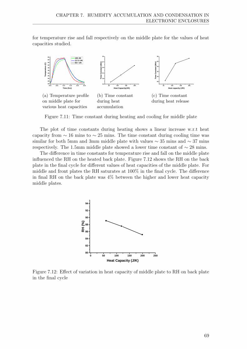
CHAPTER 7. HUMIDITY ACCUMULATION AND CONDENSATION INELECTRONIC ENCLOSURES
for temperature rise and fall respectively on the middle plate for the values of heatcapacities studied.
1 0 . 0 1 0 . 5 1 1 . 0 1 1 . 5 1 2 . 0 1 2 . 51 52 02 53 03 54 04 55 05 56 06 5
Temp
eratur
e (C)
T i m e ( h r s )
1 9 9 J / K 1 1 7 . 9 J / K 5 9 . 7 J / K
(a) Temperature profileon middle plate forvarious heat capacities
5 0 1 0 0 1 5 0 2 0 01 5
1 8
2 1
2 4
2 7
3 0
Time C
onsta
nt (M
in)
H e a t C a p a c i t y ( J / K )
(b) Time constantduring heataccumulation
5 0 1 0 0 1 5 0 2 0 0
2 8
3 0
3 2
3 4
3 6
3 8
Time C
onsta
nt (M
in)
H e a t c a p a c i t y ( J / K )
(c) Time constantduring heat release
Figure 7.11: Time constant during heating and cooling for middle plate
The plot of time constants during heating shows a linear increase w.r.t heatcapacity from ∼ 16 mins to ∼ 25 mins. The time constant during cooling time wassimilar for both 5mm and 3mm middle plate with values ∼ 35 mins and ∼ 37 minsrespectively. The 1.5mm middle plate showed a lower time constant of ∼ 28 mins.
The difference in time constants for temperature rise and fall on the middle plateinfluenced the RH on the heated back plate. Figure 7.12 shows the RH on the backplate in the final cycle for different values of heat capacities of the middle plate. Formiddle and front plates the RH saturates at 100% in the final cycle. The differencein final RH on the back plate was 4% between the higher and lower heat capacitymiddle plates.
0 5 0 1 0 0 1 5 0 2 0 0 2 5 08 0
8 2
8 4
8 6
8 8
9 0
9 2
9 4
RH (%
)
H e a t C a p a c i t y ( J / K )
Figure 7.12: Effect of variation in heat capacity of middle plate to RH on back platein the final cycle
69
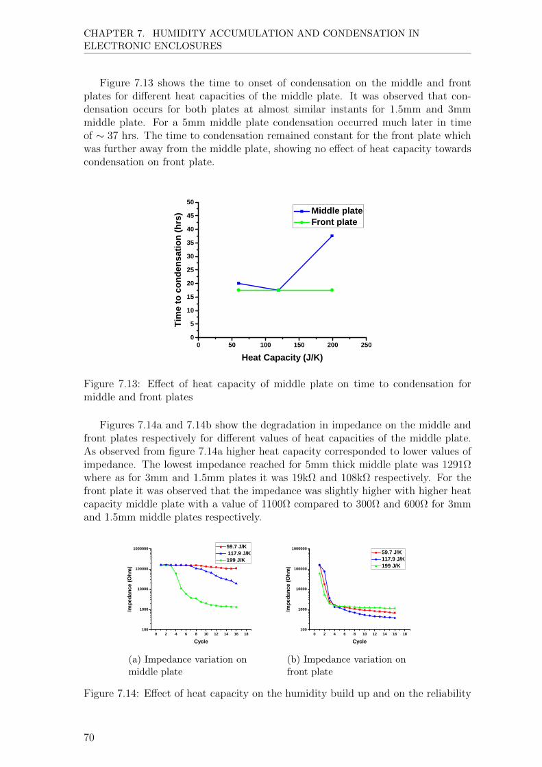
CHAPTER 7. HUMIDITY ACCUMULATION AND CONDENSATION INELECTRONIC ENCLOSURES
Figure 7.13 shows the time to onset of condensation on the middle and frontplates for different heat capacities of the middle plate. It was observed that con-densation occurs for both plates at almost similar instants for 1.5mm and 3mmmiddle plate. For a 5mm middle plate condensation occurred much later in timeof ∼ 37 hrs. The time to condensation remained constant for the front plate whichwas further away from the middle plate, showing no effect of heat capacity towardscondensation on front plate.
0 5 0 1 0 0 1 5 0 2 0 0 2 5 005
1 01 52 02 53 03 54 04 55 0
Time t
o con
dens
ation
(hrs)
H e a t C a p a c i t y ( J / K )
M i d d l e p l a t e F r o n t p l a t e
Figure 7.13: Effect of heat capacity of middle plate on time to condensation formiddle and front plates
Figures 7.14a and 7.14b show the degradation in impedance on the middle andfront plates respectively for different values of heat capacities of the middle plate.As observed from figure 7.14a higher heat capacity corresponded to lower values ofimpedance. The lowest impedance reached for 5mm thick middle plate was 1291Ωwhere as for 3mm and 1.5mm plates it was 19kΩ and 108kΩ respectively. For thefront plate it was observed that the impedance was slightly higher with higher heatcapacity middle plate with a value of 1100Ω compared to 300Ω and 600Ω for 3mmand 1.5mm middle plates respectively.
0 2 4 6 8 1 0 1 2 1 4 1 6 1 81 0 0
1 0 0 0
1 0 0 0 0
1 0 0 0 0 0
1 0 0 0 0 0 0
Impe
danc
e (Oh
m)
C y c l e
5 9 . 7 J / K 1 1 7 . 9 J / K 1 9 9 J / K
(a) Impedance variation onmiddle plate
0 2 4 6 8 1 0 1 2 1 4 1 6 1 81 0 0
1 0 0 0
1 0 0 0 0
1 0 0 0 0 0
1 0 0 0 0 0 0
Impe
danc
e (Oh
m)
C y c l e
5 9 . 7 J / K 1 1 7 . 9 J / K 1 9 9 J / K
(b) Impedance variation onfront plate
Figure 7.14: Effect of heat capacity on the humidity build up and on the reliability
70

CHAPTER 7. HUMIDITY ACCUMULATION AND CONDENSATION INELECTRONIC ENCLOSURES
7.3.4 Opening size
For experiments with enclosures of 10mm opening and 2mm diameter tube of 50mmlength, RH on the back plate and the temperatures on the plates were not influencedby the size of the opening. The peak temperature on the back plate was 83.6oC andpeak RH in the last cycle was 93% on the back plate.
Figure 7.15 shows the time to onset of condensation on the condensing middleand front plates. It can be observed that condensation occurred earlier with a biggeropening size. For the middle plate condensation occurred at 30hrs with 50mm tubeand 12.6hrs with 10mm diameter hole.
0 2 4 6 8 1 0 1 20
5
1 0
1 5
2 0
2 5
3 0
3 5
4 0
Time t
o con
dens
ation
(hrs)
H o l e ( m m )
M i d d l e p l a t e F r o n t p l a t e
T u b e
Figure 7.15: Effect of opening size on time to condensation on middle and frontplates
Figures 7.16a and 7.16b show the impedance variation on middle and front platesfor different opening sizes studied. For the middle plate in figure 7.16a the impedancecorresponding to 50mm long tube was higher than that for 10mm diameter opening.The impedance curve for 50mm long tube settled at 3kΩ where as for the enclosurewith 10mm diameter opening, the impedance settled at 1125Ω. For the case of frontplate the trend is similar with the tube shaped opening showing higher impedancethan the other two opening sizes.
71

CHAPTER 7. HUMIDITY ACCUMULATION AND CONDENSATION INELECTRONIC ENCLOSURES
- 2 0 2 4 6 8 1 0 1 2 1 4 1 6 1 81 0 0
1 0 0 0
1 0 0 0 0
1 0 0 0 0 0
1 0 0 0 0 0 0
Impe
danc
e (Oh
m)
C y c l e
1 0 m m d i a h o l e 5 0 m m l o n g t u b e
(a) Impedance variation onmiddle plate
0 2 4 6 8 1 0 1 2 1 4 1 6 1 81 0 0
1 0 0 0
1 0 0 0 0
1 0 0 0 0 0
1 0 0 0 0 0 0
Impe
danc
e (Oh
m)
C y c l e
1 0 m m d i a h o l e 5 0 m m l o n g t u b e
(b) Impedance variation onfront plate
Figure 7.16: Effect of opening size on impedance minima in each cycle for the middleplate
7.4 Discussion
Humidity accumulation was observed to occur inside the electronic enclosure due tocycling ambient temperature and internal heating. Internal heating was found tobe the dominant factor affecting RH and impedance degradation on the back plate.Larger values of separation, higher heat capacity and enclosure opening size werefound to cause higher impedance degradation and hence, higher susceptibility tohumidity related failures on the middle plate.
Figures 7.3a and 7.3b showed typical humidity and temperature profiles in theenclosure. As shown in figure 7.4 humidity accumulation was observed inside the en-closure due to natural convection between the enclosure and ambient. Condensationwas observed to occur on the middle and front plates during internal heating turn-ontimes as shown in figure 7.3a. Typical ECUs use polymers as part of electronic com-ponents and also as enclosure material [10] which can act as humidity buffers. Thehumidity absorbed is released back into the air inside the enclosure when heatingstarts, which would condense on the cooler control/logic PCB of the ECU. This pro-cess of condensation is shown to occur using hygrothermal modelling by Bayerer et.al., assuming only diffusion mode of mass transport [18]. Another source of humidityreleased during heating is water vapour adsorbed on walls of enclosure and PCBA.Condensation occurred for longer durations on the middle plate than the cooler frontplates. This was because during heating turn-on time absorbed/adsorbed humidityis released more from the vicinity of the heated back plate and condenses first on themiddle plate as it is nearest cooler surface encountered. Impedance was observed todecrease on the condensing middle and front plates due to humidity accumulationinside the enclosure over successive temperature cycles.
RH on the heated back plate decreased with higher power dissipation on it as seenfrom figure 7.6a. In the final cycle of the experiment the RH near the back plate wasstill above 90% for power dissipation of 14.5W. PCBA manufactured with DL-Malicacid and glutaric acid based no-clean solder fluxes experience considerable leakagecurrents when RH is above the respective DRH[8][9]. For a PCBA which has usedDL-Malic or glutaric acid based no-clean solder fluxes for component assembly wouldnot encounter leakage currents and ECM on the back plate for a power dissipationof 14.5W even though the DRH for DL-Malic acid and glutaric acids are lower than
72

CHAPTER 7. HUMIDITY ACCUMULATION AND CONDENSATION INELECTRONIC ENCLOSURES
90% because of the effect of heating. As observed from figure 7.8a, this shows a wayto improve reliability on the three plates by heating. From figure 7.8a it can alsobe observed that impedance gradually decreased for a power dissipation of 2.5W,showing that this level of internal heating was not enough to improve reliabilityon the back plate. To prevent humidity related reliability degradation on the backplate a threshold power dissipation between 2.5W and 14.5W is required even thoughcondensation was avoided by internal heating of 2.5W. Spending 14.5W to improvereliability would result in inefficient humidity control. The type of heating usedin this work was convective heating. Hence, more efficient methods of heating likeradiant heating or preferential condensation could be used to decrease humidity andattain required reliability. For the middle and front plates impedance decreased oversuccessive cycles even for 14.5W internal heating on the back plate as observed fromfigures 7.8b and 7.8c. But, power dissipation delayed the onset of condensation onmiddle and front plates as seen from figure 7.7. It was also observed that powerdissipation was the dominant parameter that determined the peak RH on the backplate, with the other parameters studied like separation, heat capacity and openingsize having only minimal and no effect respectively.
With increase in separation between the heated back plate and middle plate, adecrease in temperature was observed on the back and middle plates. This was dueto an increase in convection heat transfer from the plates due to increased separation.This decrease in temperature contributed to a corresponding increase in RH on theback plate as shown in figure 7.9a. When separation of the middle plate w.r.t heatedback plate was increased, time to onset of condensation on the middle plate decreasedas seen from figure 7.10a due to lower surface temperatures. The impedance curvesfor the middle plate showed improvement in reliability only for a separation of 5mmfrom the heated back plate while, for 20mm and 35mm separation the impedancedecreased over successive cycles as seen from figure 7.10b. This implies that there isa critical value of separation of the middle plate from the heated back plate beyondwhich impedance degrades for a particular power dissipation. Therefore, a criticalelectronic component or control/logic PCB could be protected from humidity failuresby suitable positioning it w.r.t a power dissipating component.
Higher heat capacity on the middle plate delayed the rise and fall of temperatureon it as observed from figure 7.11. According to figure 7.13 higher heat capacity of5mm middle plate (199J/K) prolonged the onset of condensation. Even though timeto onset of condensation was prolonged as shown in figure 7.13, the impedance andreliability was lower for a higher heat capacity middle plate as observed from figure7.14a. This was because of the low swing in peak to peak values of RH near the higherheat capacity middle plate due to sluggish rise and fall of temperature. This impliesthat electronic circuits situated on high heat capacity components like heat sinkswould experience reliability issues especially if low DRH WOA based solder fluxeswere used in PCBA manufacturing[16]. The high heat capacity middle plate alsoprovided slight improvement in reliability for the front plate even though 35mm awayas seen from figure 7.14b. This was because the higher heat capacity middle platestored more heat energy during heating phase and released it during low temperaturephase to keep the front plate comparatively warmer. In this particular case the heatcapacity of aluminium middle plate was not enough to store enough thermal energyto prevent further impedance degradation on the front plate. The study on effect ofheat capacity suggests utilising it as a passive humidity control technique by using
73

CHAPTER 7. HUMIDITY ACCUMULATION AND CONDENSATION INELECTRONIC ENCLOSURES
high heat capacity/low form-factor phase-change material modules.The effect of higher opening size was observed to hasten onset of condensation
and degrade impedance. This can be explained by the fact that bigger opening sizesallow higher flow due to natural convection between the enclosure and the ambient.This resulted in faster accumulation of humidity in the enclosure with 10mm openingsize. Faster accumulation of humidity inside an electronic enclosure with largeropening size was also demonstrated by conseil et. al.[16]. The resistance of the 50mmtube to humidity transfer is higher than that of the 10mm diameter opening. Hence,condensation occurred in the enclosure with the 50mm tube much later in time. Also,slower accumulation of humidity inside the enclosure with the tube as opening causedhigher impedance on the SIR pattern compared to 10mm diameter opening. So,smaller opening sizes should be preferred on electronic enclosures to reduce effect ofreliability degradation to humidity related failures. Controlled openings are providedin electronic enclosures as drain holes, forced convection holes, pressure equalizationetc. Drain holes need to be minimum 3mm in diameter to prevent water dropsblocking the hole due to surface tension. Pressure equalisation hole of a particulardiameter could be replaced with a tube of same diameter such that the resistanceto humidity transfer is increased leading to longer time to condensation and lowerdegradation in impedance.
This work has investigated the dependence of power dissipation and other ge-ometric parameters on humidity accumulation and reliability in an electronic en-closure. The current work can also be interpreted as a study of using intermittantinternal heating for humidity control. Heating as humidity control method has beeninvestigated in literature before[19][20]. But as shown in this work, convective heat-ing might not be feasible in all situations in electronics due to its low efficiency.More efficient heating methods like radiant heating needs to be explored. Radiantheating is already being used in building space heating applications[21][22]. Use ofheat capacity to keep components warm and improve reliability has been demon-strated in figure 7.14b. Phase-change materials could be used for this purposebecause they have very high heat capacity and small size. Phase-change materialscould be used in an electronic enclosure to absorb a part of the power dissipated byelectronic components and then used to keep critical circuits warm during off-timeof the device. Phase-change materials have been shown to improve the thermalperformance of electronics in literature[23][24]. For a particular power dissipationinside an electronic enclosure, by choosing proper values for the enclosure packagingrelated parameters studied here and proper choice of humidity control techniquesreliability of electronics to humidity related failures can be improved.
7.5 Conclusion
Humidity accumulation, condensation and reliability degradation due to cycling am-bient temperature and internal heating was studied. The humidity profiles on backplate and time to onset of condensation was investigated on the middle and frontplates. Reliability due to humidity failures was studied by impedance degradationof contaminated SIR patterns. The following conclusions can be derived from thiswork :
• Cycling ambient temperature and internal heating caused a cycle by cycle
74

CHAPTER 7. HUMIDITY ACCUMULATION AND CONDENSATION INELECTRONIC ENCLOSURES
humidity accumulation inside the electronic enclosure. Condensation occurredon the cooler middle and front plates during the internal heating turn on timedue to release of absorbed and adsorbed water vapour. Reliability as denotedby impedance of SIR patterns decreased over the duration of the experiment.
• Internal heating improved reliability on the heated plate for an internal powerdissipation of 14.5W but, not on the middle and front plates. This shows thatinternal heating can be a method to improve reliability inside an electronicenclosure. Also, the higher amount of energy needed for this while using con-vective heating shows that more efficient heating methods like radiant heatingwould be more feasible for use in electronic enclosures.
• For a separation of 5mm from the heated back plate, impedance on the middleplate remained steady . This shows that reliability of a component or circuit onthe can be improved by suitably placing it with respect to a power dissipatingsource inside an electronic enclosure.
• For higher heat capacity middle plate, impedance of the degraded over succes-sive temperature cycles. This shows that circuits placed on high heat capacitycomponents can experience degradation in reliability due to humidity. Pres-ence of high heat capacity components can also cause a slight improvement inreliability for circuits in its vicinity due to release of stored thermal energy.
• Enclosures with smaller openings having higher resistance to convective flowslike tubes experience lower drop in impedance over successive temperaturecycles. So, Smaller opening sizes for enclosures should be preferred for betterreliability to humidity related failures.
7.6 Acknowledgement
This research was conducted as part of the IN SPE project funded by InnovationFund Denmark and CELCORR(www.celcorr.com). The authors would like to ac-knowledge the funding and help received from the consortium partners.
75

Bibliography
[1] R. Hienonen, R. Lahtinen, Corrosion and climatic effects in electronics, VTTPublications, 2000.
[2] D. Minzari, ”Investigation of electronic corrosion mechanisms,” Ph.D disserta-tion, Technical University of Denmark, Kgs. Lyngby, 2010.
[3] B. Rudra, M. Pecht, D. Jennings, ”Assessing time-to-failure due to conductivefilament formation in multi-layer organic laminates”, IEEE Transactions onComponents, Packaging and Manufacturing Technology : part B, vol. 17, no.3, pp. 269–276, Aug. 1994.
[4] C. Schimpf, K. Feldmann, C. Matzner, A. Steinke, ”Failure of electronic devicesdue to condensation”, Microsystem Technologies, Vol. 15, Issue 1, pp. 123–127,2009.
[5] M. Tencer, Moisture Ingress into Nonhermetic Enclosures and Packages.AQuasi-Steady State Model for Diffusion and Attenuation of Ambient Humid-ity Variations, Electronic components and technology conference, pp. 196–209,1994.
[6] H. Conseil, M. S. Jellesen, R. Ambat, ”Contamination profile on typical printedcircuit board assemblies vs soldering process”, Soldering and Surface MountTechnology, Issue 4, Vol. 26, pp. 194–202, 2014.
[7] R. B. Comizzoli, C. A. Jankoski, G. A. Peins, L. A. Psota-Kelty, D. J. Siconolfi,J. D. Sinclair, ”Reliability of electronics in harsh environments: Electrical leak-age and corrosion caused by hygroscopic pollutant particles”, Elec trochemicalsociety proceedings, Issue 29, Vol. 99, pp. 186–193, 1999
[8] V. Verdingovas, M. S. Jellesen and R. Ambat, ”Relative effect of solder fluxchemistry on the humidity related failures in electronics,” Soldering and SurfaceMount Technology, Vol. 27, Issue 4, pp. 146–156, 2015.
[9] V. Verdingovas, M. S. Jellesen, R. Ambat, ” Solder Flux Residues andHumidity-Related Failures in Electronics: Relative Effects of Weak OrganicAcids Used in No-Clean Flux Systems,” Journal of electronic materials, vol.44,Issue 4, pp. 1116–1127, 2015.
[10] H. Conseil-Gudla, Z. Staliulionis, M. S. Jellesen, M. Jabbari, J. H. Hattel,R. Ambat, ” Humidity build-up in electronic enclosures exposed to constantconditions,” IEEE transactions on components packaging and manufacturingtechnology, vol.7, Issue 3, pp. 412–423, 2017.
76

BIBLIOGRAPHY
[11] C. Sintamarean, F. Blaabjerg, H. Wang, Y. Yang, ”Real Field Mission ProfileOriented Design of a SiC-Based PV-Inverter application”, IEEE Transactionson Industry Applications, Vol. 50, Issue 6, pp. 4082–4089, 2014.
[12] T. Lee, B. Chambers, M. Mahalingam, ”Application of CFD Technology toElectronic Thermal Management”, IEEE Transactions on Components Pack-aging and Manufacturing Technology, vol. 18, No. 3,1995.
[13] A. Ortega, B. Lall, J. Chicci, M. Aghazadeh, ”Heat transfer in a low aspectratio horizontal enclosure for laptop computer application”, Proc. of NinthSEMI-THERM, pp. 42-49, 1993.
[14] B.S. Lall, A. Ortega, H. Kabir, ”Thermal design rules for electronic componentson conducting boards in passively cooled enclosures”, Thermal Phenomena inElectronic Systems 1994. I-THERM IV. Concurrent Engineering and ThermalPhenomena. InterSociety Conference on, pp. 50-61, 1994.
[15] S. Joshy, M. S. Jellesen, R. Ambat, ”Effect of interior geometry on local climateinside an electronic device enclosure”, 16th IEEE Intersociety Conference onThermal and Thermomechanical Phenomena in Electronic Systems (ITherm),pp. 779–783, 2017
[16] H. Conseil, V. C. Gudla, M. S. Jellesen, R. Ambat, Humidity build-up in atypical electronic enclosure exposed to cycling conditions and effect on corrosionreliability, IEEE Transactions on Components, Packaging and ManufacturingTechnology, vol. 6, Issue 9, pp. 1379–1388, 2016.
[17] Sensirion, Application Note Dew-point calculation, pp.1-3, Available :http://irtfweb.ifa.hawaii.edu/˜tcs3/tcs3/Misc/Dewpoint Calculation HumiditySensor E.pdf [Accessed : 03-April-2019]
[18] R. Bayerer, M. Lassmann, S. Kremp, ”Transient Hygrothermal-Response ofPower Modules in Inverters - The Basis for Mission Profiling under Climateand Power Loading”, IEEE Transactions on Power Electronics, vol. 31, Issue.1, pp. 613-620, 2016.
[19] M. Tencer, J. S. Moss, “Humidity Management of Outdoor Electronic Equip-ment: Methods, Pitfalls, and Recommendations,” IEEE Trans. Componentsand Packaging Tech., Vol. 25, No. 1 (2002), pp. 66-72.
[20] I. Belov, M. Lindgren, J. Ryden, Z. Alavizadeh, P. Leisner, “CFD assisted de-sign evaluation and experimental verification of a logic controlled local PCBheater for humidity management in electronics enclosure,” International Ther-mal, Mechanical and Multi-Physics Simulation, and Experiments in Microelec-tronics and Microsystems (EuroSimE), 2010.
[21] D. Anastaselos, I. Theodoridou, A. M.Papadopoulos, M. Hegger, ”Integratedevaluation of radiative heating systems for residential buildings”, Energy, vol.36, no. 7, pp. 4207-4215, 2011.
[22] M. Bojic, D. Cvetkovic, M. Miletic, J. Malesevic, H. Boyer, ”Energy, cost,and CO2 emission comparison between radiant wall panel systems and radiatorsystems”, Energy and Buildings, vol. 54, pp. 496-502, 2012.
77

BIBLIOGRAPHY
[23] M. J. Vesligaj, C. H. Amon, ”Transient thermal management of tempera-ture fluctuations during time varying workloads on portable electronics”, IEEETransaction on Components and Packaging Technology, vol. 22, no. 4, pp. 541-550, 1999.
[24] E. M. Alawadhi, C. H. Amon, ”PCM thermal control unit for portable electronicdevices: experimental and numerical studies”, IEEE transaction on componentand packaging technologies, vol. 26, no. 1, pp. 116-125, 2003.
78

Chapter 8
Humidity profile inside electronicenclosures with retained water
This work studies the effect of enclosure hole size and inter PCB spacing on temper-ature and humidity inside an electronic enclosure under constant heating conditionsand in the presence of retained liquid water. Liquid water can be present in elec-tronic enclosures due to rain, during servicing of the product, condensation insidethe enclosure etc. The enclosure has three parallel aluminium plates which simu-lates PCBA in an electronic unit. Humidity and temperature profiles under constantheating was studied by applying a slow ramp of internal power dissipation on one ofthe plates. The humidity and temperature profiles were found to depend on PCBspacing and enclosure hole size.
8.1 Materials and methods
The experimental setup consisted of an aluminium enclosure with parallel arrange-ment of aluminium plates simulating PCBs. The enclosure size was 263mm x 162mmx 91mm and the aluminium plates were 180mm x 90mm x 1.5mm. The plates hadRH and temperature sensors placed on their mid-points. The plates also had SIRpatterns contaminated with 15.6µg/cm2 placed on them. A Biologic VSP series in-strument was used to monitor the impedance at a fixed frequency of 20KHz. One ofthe plates - back plate has a mat heater pasted on it. The back plate is 10mm fromthe enclosure wall. The middle plate is varied in separation from 7.5mm, 11.25mmand 15mm from the back plate. The front plate is 60mm from the back plate. 100mlof liquid water was added in the enclosure to simulate retained water. When hu-midity saturates inside the enclosure, the voltage applied to the resistive mat heaterwas varied at a slow rate of 20mV/2min so that, at any instant the RH and temper-ature measured by the sensors would be steady state values for the heating powerat that instant. The experiment was conducted under conditions of 24C and 50%RH. Figure 8.1 shows the experimental setup.
79

CHAPTER 8. HUMIDITY PROFILE INSIDE ELECTRONIC ENCLOSURES WITHRETAINED WATER
Figure 8.1: Schematic diagram of enclosure with parallel plates and retained water
8.2 Results
8.2.1 Effect of PCB separation
Figure 8.2a shows the variation in RH and temperature measured on the middleplate for different separations when the back plate was at 50oC. The temperaturedecreased on the middle plate from 41.2oC at 7.5mm separation to 38.6oC at 15mm.This decrease in temperature was due to better heat removal by convection from theback plate with larger separation from the middle plate. The decrease in temperaturecaused a corresponding increase in RH from 58.8% to 87.2%. Figure 8.2b shows theimpedance change on the middle plate during the course of the experiment. It wasobserved that impedance showed minimal drop in value with lower separation of7.5mm compared to larger separations of the middle plate and back plate. This wasdue to lower RH and higher temperature on middle plate with 7.5mm separation asseen from figure 8.2a.
5 . 0 7 . 5 1 0 . 0 1 2 . 5 1 5 . 0 1 7 . 5 2 0 . 03 8 . 0
3 8 . 5
3 9 . 0
3 9 . 5
4 0 . 0
4 0 . 5
4 1 . 0
4 1 . 5
4 2 . 0
T e m p e r a t u r e
Temp
eratur
e (C)
S e p a r a t i o n ( m m )5 5
6 0
6 5
7 0
7 5
8 0
8 5
9 0
9 5 R H
RH (%
)
(a)
0 2 4 6 8 1 0 1 2 1 4 1 6 1 8 2 00
5 0 0 0 0
1 0 0 0 0 0
1 5 0 0 0 0
2 0 0 0 0 0 1 5 m m
Impe
danc
e (Oh
m)
T I M E ( h r s )
1 1 . 2 5 m m 7 . 5 m m
(b)
Figure 8.2: a) RH and temperature variation for different separations b) Impedancedegradation on middle plate for different separations from the heated plate
80

CHAPTER 8. HUMIDITY PROFILE INSIDE ELECTRONIC ENCLOSURES WITHRETAINED WATER
8.2.2 Effect of hole size
Figure 8.3 shows the effect of enclosure hole size on RH and temperature on themiddle plate when the back plate was at 50oC. The temperature on the middleplate was similar at 39.8oC for hole sizes of 2mm and 10mm. For the enclosurewithout any holes, the temperature measured on the middle plate was 41.2oC. TheRH measured on the middle plate increased from 77.6% for no hole to 82.5% for a10mm hole.
0 2 4 6 8 1 0 1 23 9 . 5
4 0 . 0
4 0 . 5
4 1 . 0
4 1 . 5
T e m p e r a t u r e
Temp
eratur
e (C)
H o l e s i z e ( m m )5 5
6 0
6 5
7 0
7 5
8 0
8 5
9 0
9 5 R H
RH (%
)
Figure 8.3: Effect of hole size on RH and temperature on the middle plate fordifferent enclosure hole sizes
8.3 Conclusion
• A smaller separation between the back plate and middle plate resulted inhigher temperature and lower RH on the middle plate. The lower separationalso helped prevent degradation of impedance on the SIR pattern, showingimprovement in reliability to humidity related failures.
• A bigger hole size contributed to lower RH on the middle plate due to slightdecrease in temperature with increasing hole size.
81

Chapter 9
Circuit analysis to predicthumidity related failures inelectronics - Methodology andrecommendations
Abstract
Aim of this paper is to demonstrate the use of circuit analysis to predict humidityrobustness of an electronic circuit design. There is a lack of design tools whichcan predict failures due to humidity, especially the effect of humidity on electricalfunctionality of circuits. This work provides a methodology for utilising circuitsimulation tools to detect humidity related faults associated with a circuit design byusing experimentally determined leakage current data or surface insulation resistanceusing test pattern or model circuits. Simulation of circuits were performed with theexperimentally determined SIR value as a parasitic resistance across two nodes of thecircuit. Commonly used circuits such as a differential amplifier and a non-invertingcomparator were analysed by this methodology. Based on the analysis, circuits withhigher humidity robustness have been suggested as examples to demonstrate theeffectiveness of this methodology. Finally, the correlation between the propertiesof the water layer on SIR pattern and actual components was done, which furtherdemonstrates the applicability of the methodology.
Keywords: Electronic circuit, Humidity, Contamination, Surface insulation re-sistance, Leak current.
Published as: S. Joshy, V. Verdingovas, M. S. Jellesen, R. Ambat, ”Circuit analysis
to predict humidity related failures in electronics - Methodology and recommendations”,
Microelectronics Reliability, Vol. 93, pp. 81-88, Feb. 2019
82
CHAPTER 9. CIRCUIT ANALYSIS TO PREDICT HUMIDITY RELATEDFAILURES IN ELECTRONICS - METHODOLOGY AND RECOMMENDATIONS
9.1 Introduction
Electronic devices are used nowadays in variety of climatic conditions. Some ofthe applications are in controlled indoor climate, but others are exposed to harshconditions like humid offshore locations, hot engine compartments of automobiles,atmospheres with corrosive gases etc. Application of electronics in harsh climateshave shown failure modes due to high temperature[1][2], high humidity[3][4], gaseouscorrosion[5][6], atmospheric contamination[7][8][9], and their combination. The fail-ures due to humidity are aggravated by the recent drive towards miniaturisationand low-power consumption. Currently, robustness of electronic products to hu-midity is incorporated in the industry using prior knowledge of failures. There is alack of simulation and analysis tools which can predict the effect of humidity andcontamination on the electrical functionality of the circuit.
High humidity can accumulate inside electronic enclosures under both constantand cycling conditions of ambient temperature[10][11]. High humidity can also resultfrom release of adsorbed and absorbed water from the walls of the enclosure[10].Various mechanisms of humidity ingress into electronic enclosures is summarised byJacobsen et.al.[14]. Presence of water vapour in the air can lead to formation of thinlayer of water on a surface. The average number of monolayers of gas adsorbed on asurface is described by Brunauer-Emmett-Teller (BET) theory[12]. Thickness of thewater layer increases with increasing humidity and becomes visible under condensingconditions. Thick water layer containing dissolved ions on a Printed circuit boardassembly(PCBA) leads to significant increase in leakage currents and failure modessuch as electrochemical migration (ECM)[15][16][17][18].
A thicker layer of water could form on a PCBA surface even under non-condensingconditions in the presence of hygroscopic contamination. The PCBA manufacturingand component assembly process adds hygroscopic residues to the PCBA surface.Even no-clean solder fluxes used for component assembly leaves behind hygroscopicand ionic weak-organic acids (WOA) on the PCBA surface capable of causing signif-icant leakage currents[19][20]. Commercially available solder flux systems commonlyuse WOAs as the activator component of the flux. WOAs like DL-malic acid presenton PCBA can cause ECM failures even at RH of 80%[21][22].
The properties of water layer formed on a PCBA can be studied electrically bymonitoring the leakage current or impedance of an SIR pattern[23][24]. The value ofleak current could be monitored for different climatic conditions of RH and PCBA-surface contamination levels. This empirical data represents the behaviour of thewater layer on a PCBA under different conditions of RH and WOA concentrations.Using this experimentally determined leakage-current data, the effect of formationof the water-layer and its electrical interference on the PCBA functionality can bemodelled as a parasitic resistance[25]. This parasitic resistance could be included inanalysis of a circuit using standard circuit simulation tools to predict the effect ofhumidity and contamination on its functionality.
Circuit analysis to determine the effect of humidity and contamination on func-tionality of electronic circuits has been demonstrated in our earlier publications[25][26].This paper has analysed more generic circuits using the above methodology andshowed how the circuit modifications in such cases could improve the humidity ro-bustness. The paper also evaluated the validity of using the leakage-current datafrom standard SIR patterns for this analysis. The circuits analysed in this paper for
83

CHAPTER 9. CIRCUIT ANALYSIS TO PREDICT HUMIDITY RELATEDFAILURES IN ELECTRONICS - METHODOLOGY AND RECOMMENDATIONS
demonstration are a differential amplifier and a non-inverting comparator. Leakagecurrent data from SIR patterns contaminated with adipic acid and DL-malic acid,representing two extreme type no-clean solder flux residues from the point of view ofaggressiveness are used for the analysis. Adipic acid is less corrosive because it haslower solubility in water and higher deliquescence RH (DRH) whereas, DL-Malicacid is highly soluble and has a lower DRH which makes it more corrosive. Sensi-tivity of both the differential amplifier and non-inverting comparator are comparedfor conditions in which the PCBA is made using adipic or DL-malic acid basedno-clean flux and residues are remaining on the surface. Alternate circuit designswhich are more tolerant to humidity-related failures are suggested which includean instrumentation amplifier and an inverting comparator. Also shown are designmodifications like splitting of bigger resistances to multiple smaller resistances tomake the circuits more robust to humidity. The experimentally determined datafrom SIR pattern is compared with that of land patterns of actual components withpackage dimensions 0402, 0603 and 0805 to demonstrate the validity of using datafrom standard SIR patterns. PCBAs contaminated with succinic and glutaric acidsare used for this comparison. Data from the actual components agree with the datafrom SIR pattern for both WOAs within an order of magnitude of leakage current.
9.2 Extraction of SIR data for circuit analysis
from humidity experiments
The experimental data which describes the properties of water layer on PCBAcomes from our earlier work[21]. The SIR patterns used were FR-4 PCBAs of size13mmx25mm and pitch size of 0.3mm. The surface concentrations of WOAs on theSIR pattern used for the studies were 25µg/cm2, 50µg/cm2 and 75µg/cm2. Leak-age current measurements were done with the SIR patterns placed in an ESPECPL-3KPH climatic chamber at different levels of humidity and applied d.c voltage.Further details of the experiment design, methods and materials can be found elsewhere[21][25].
The leakage current data from the experiments were converted to equivalent SIRfor applied voltage of 5V. The SIR data thus obtained for adipic and DL-malic acidsat various humidity levels are shown in tables 9.1 and 9.2.
As seen from the data, SIR values drop with increasing values of RH and WOAsurface concentrations for both adipic and DL-malic acid. The SIR drops drasticallybeyond the DRH of the WOA which is around 80% for DL-malic acid and 98%for adipic acid. The decrease in resistance is more pronounced for SIR patternscontaminated with DL-malic acid as expected due to its higher solubility in watercompared to adipic acid. The data in tables 9.1 and 9.2 are used for analysis ofcircuits in this paper.
To correlate the leakage current data from SIR pattern with that on actual com-ponents, leakage current measurements were done on land patterns of surface-mountcomponents placed on a test PCBA described elsewhere[27]. The WOAs used forthis test were succinic acid and glutaric acid. The test PCBA contains land patternsfor surface mount component sizes of 0402, 0603, 0805 and an SIR pattern on thesame PCBA. The test PCBA was contaminated with WOA at the surface with aconcentration of 100µg/cm2. The test PCBA was placed in the ESPEC PL-3KPH
84

CHAPTER 9. CIRCUIT ANALYSIS TO PREDICT HUMIDITY RELATEDFAILURES IN ELECTRONICS - METHODOLOGY AND RECOMMENDATIONS
Table 9.1: SIR data for different values of RH and concentration of adipic acid at25oC and d.c electrical input
RH SIR(MΩ) SIR(MΩ) SIR(MΩ)25µg/cm2 50µg/cm2 75µg/cm2
60 5209.29 3090.5 2789.4870 4945.24 2157.70 1665.3680 2865.82 1204.58 922.4590 504.23 494.56 449.6495 209.69 263.49 293.2198 157.32 133.65 194.9199 102.78 45.73 23.79
Table 9.2: SIR data for different values of RH and concentration of DL-Malic acidat 25oC and d.c electrical input
RH SIR(MΩ) SIR(MΩ) SIR(MΩ)25µg/cm2 50µg/cm2 75µg/cm2
60 2902.40 1634.53 602.4070 2587.40 303.69 39.9380 2071.03 21.12 3.1890 781.92 1.58 0.4295 151.02 0.65 0.3298 30.83 0.55 0.3299 6.62 0.52 0.28
85

CHAPTER 9. CIRCUIT ANALYSIS TO PREDICT HUMIDITY RELATEDFAILURES IN ELECTRONICS - METHODOLOGY AND RECOMMENDATIONS
environment chamber with required potential bias and subjected to different humid-ity profile as required. The leakage current across the component land-patterns andSIR pattern on the test PCBA were measured using a VSP Biologic potentiostat.The following section describes the comparison of leakage current data from SIRand components.
9.3 Comparison of leak-current level from SIR
and component testing
Leakage currents were measured across surface-mount land-patterns of sizes 0402,0603 and 0805 at a contamination surface concentration of 100µg/cm2. Figures 1and 2 show how the SIR values compare to resistances across actual components forsuccinic and glutaric acid respectively as contamination. Succinic acid and adipicacid has similar DRH of around 98%. Glutaric acid has a lower DRH of around83%, near to that of Malic acid. Its solubility is also similar to that of DL-Malicacid of around 1400g/L of water at 25oC[21].
5 5 6 0 6 5 7 0 7 5 8 0 8 5 9 0 9 5 1 0 01 E - 1 2
1 E - 1 1
1 E - 1 0
1 E - 9
1 E - 8
1 E - 7
1 E - 6
1 E - 5
1 E - 4
S I R p a t t e r n 0 4 0 2 0 6 0 3 0 8 0 5
Leak
age C
urren
t (mA)
R H ( % )
(a)
5 5 6 0 6 5 7 0 7 5 8 0 8 5 9 0 9 5 1 0 01 E - 1 2
1 E - 1 1
1 E - 1 0
1 E - 9
1 E - 8
1 E - 7
1 E - 6
1 E - 5
1 E - 4
S I R P a t t e r n 0 4 0 2 0 6 0 3 0 8 0 5
Leak
age C
urren
t (mA)
R H ( % )
(b)
Figure 9.1: Comparison of leakage-current from SIR and actual components for a)Succinic acid b) Glutaric acid as contamination at 25oC and d.c electrical input.
For succinic acid it was seen that the leakage-current values for the SIR andland-patterns are within an order of magnitude of each other in the full range ofRH as shown in figure 9.1a. For glutaric acid, the leakage-current values for SIRpattern and land-patterns are also within an order of magnitude of each other untilthe DRH of glutaric acid of 83-89%. Beyond the DRH of glutaric acid, the SIRpattern showed higher leakage current. For RH higher than DRH, the resistance ofSIR pattern was two orders of magnitude lower compared to land-patterns as shownby figure 9.1b. So, the method of using resistance of water layer from SIR valuesfor analysis with electronic circuits is a valid approximation for succinic acid in theentire range of RH upto 100%. For Glutaric acid, the approximation is valid untilDRH beyond which the accuracy of the SIR data degrades.
86
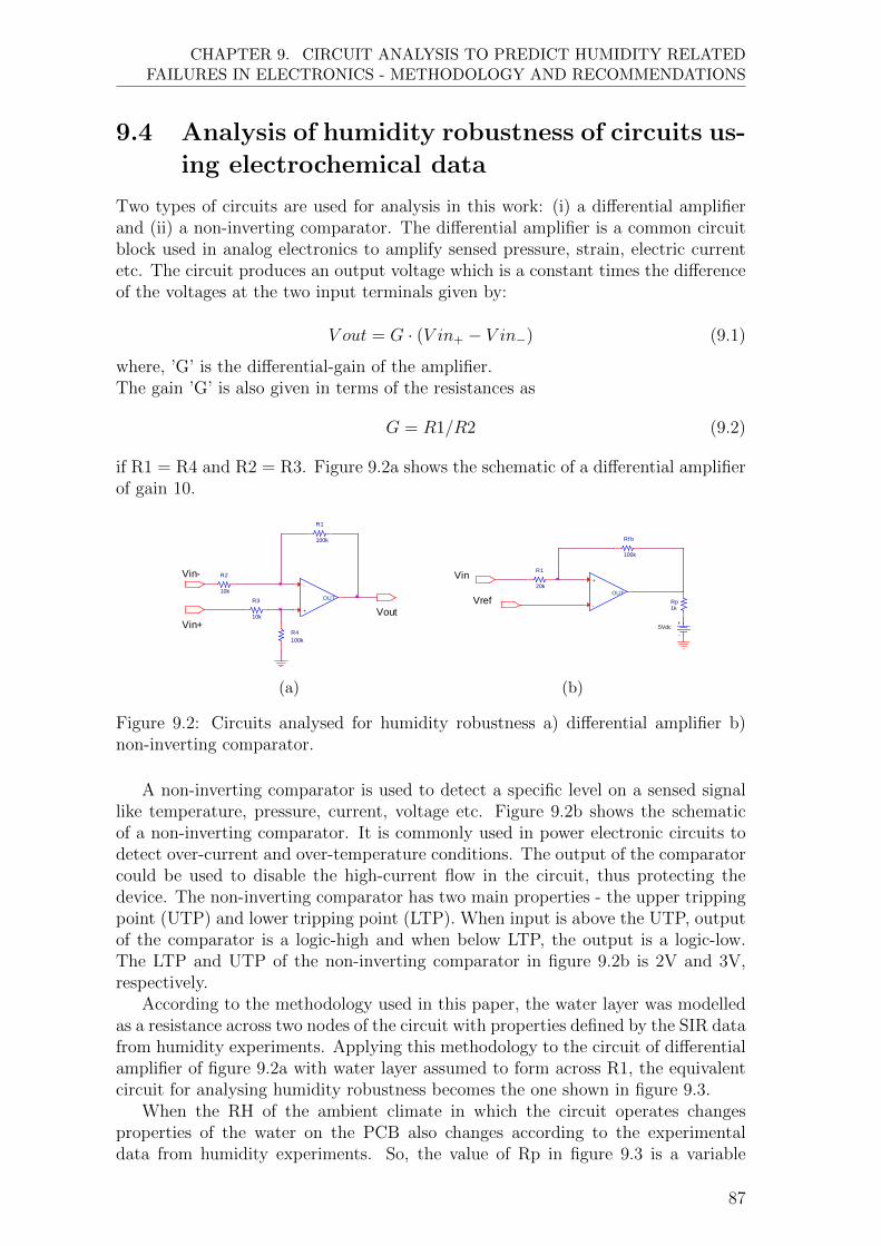
CHAPTER 9. CIRCUIT ANALYSIS TO PREDICT HUMIDITY RELATEDFAILURES IN ELECTRONICS - METHODOLOGY AND RECOMMENDATIONS
9.4 Analysis of humidity robustness of circuits us-
ing electrochemical data
Two types of circuits are used for analysis in this work: (i) a differential amplifierand (ii) a non-inverting comparator. The differential amplifier is a common circuitblock used in analog electronics to amplify sensed pressure, strain, electric currentetc. The circuit produces an output voltage which is a constant times the differenceof the voltages at the two input terminals given by:
V out = G · (V in+ − V in−) (9.1)
where, ’G’ is the differential-gain of the amplifier.The gain ’G’ is also given in terms of the resistances as
G = R1/R2 (9.2)
if R1 = R4 and R2 = R3. Figure 9.2a shows the schematic of a differential amplifierof gain 10.
+
-
OUT
Vin-
Vin+
Vout
R1
100k
R2
10k
R3
10k
R4
100k
(a)
Vref
Vin
5Vdc
Rp1k
R1
20k
Rf b
100k
+
-
OUT
(b)
Figure 9.2: Circuits analysed for humidity robustness a) differential amplifier b)non-inverting comparator.
A non-inverting comparator is used to detect a specific level on a sensed signallike temperature, pressure, current, voltage etc. Figure 9.2b shows the schematicof a non-inverting comparator. It is commonly used in power electronic circuits todetect over-current and over-temperature conditions. The output of the comparatorcould be used to disable the high-current flow in the circuit, thus protecting thedevice. The non-inverting comparator has two main properties - the upper trippingpoint (UTP) and lower tripping point (LTP). When input is above the UTP, outputof the comparator is a logic-high and when below LTP, the output is a logic-low.The LTP and UTP of the non-inverting comparator in figure 9.2b is 2V and 3V,respectively.
According to the methodology used in this paper, the water layer was modelledas a resistance across two nodes of the circuit with properties defined by the SIR datafrom humidity experiments. Applying this methodology to the circuit of differentialamplifier of figure 9.2a with water layer assumed to form across R1, the equivalentcircuit for analysing humidity robustness becomes the one shown in figure 9.3.
When the RH of the ambient climate in which the circuit operates changesproperties of the water on the PCB also changes according to the experimentaldata from humidity experiments. So, the value of Rp in figure 9.3 is a variable
87

CHAPTER 9. CIRCUIT ANALYSIS TO PREDICT HUMIDITY RELATEDFAILURES IN ELECTRONICS - METHODOLOGY AND RECOMMENDATIONS
Rp – Parasitic resistance
due to water-layer
formation
+
-
OUT
Vin-
Vin+
Vout
R1
100k
R2
10k
R3
10k
R4
100k
Rp
Figure 9.3: Model of water layer formation across resistor R1 of differential amplifier
with respect to ambient RH. Similar logic applies to the effect of contaminationsurface concentration on Rp. The following sub-sections discuss in detail the effectof humidity and contamination on the sensitivity of differential amplifier and non-inverting comparator circuits. Orcad Capture CIS was used in this work for circuitsimulation.
To simulate the effects of humidity and contamination, a differential sine voltageof 0.1V and 1kHz a.c is applied across the terminals Vin+ and Vin- of the differentialamplifier circuit shown in figure 9.2a. The nominal output of the circuit in figure9.3 for the above mentioned input is a sine wave of 1V in amplitude, correspondingto the gain of 10. When water layer forms across a resistance, the net resistance ofthe parallel combination with the parasitic resistance Rp due to the water layer islower than the individual resistances. So, if water layer forms across R1 or R4 theeffect would be to reduce the gain ’G’ according to equation 9.2. But if the waterlayer is across R2 or R3 the gain would increase.
To study effect of humidity and contamination on a non-inverting comparator,the water layer is assumed to form on resistors Rfb and R1 of figure 9.2b. A 5Vpeak-to-peak amplitude sine wave of 1kHz frequency and 2.5V d.c offset is appliedas the input.
9.4.1 Humidity robustness of differential amplifier circuit
The effect of humidity and contamination on the functionality of differential ampli-fier is simulated assuming water layer formation across the terminals of one com-ponent only at a time. With this assumption the differential amplifier circuit issimulated for humidity and contamination effects on resistors R1 and R2. Figures9.4a and 9.4b show the variation in differential gain for different climatic conditionsof RH and DL-Malic acid for the components R1 and R2 in the circuit of figure 9.2a.
It is seen from figures 9.4a and 9.4b that the absolute value of error in gainincreases with increasing RH. For DL-Malic acid, which represents residue from an
88

CHAPTER 9. CIRCUIT ANALYSIS TO PREDICT HUMIDITY RELATEDFAILURES IN ELECTRONICS - METHODOLOGY AND RECOMMENDATIONS
6 0 7 0 8 0 9 0 1 0 0- 5
0
5
1 0
1 5
2 0
2 5 2 5 µg / c m 2
5 0 µg / c m 2
7 5 µg / c m 2
Gain
error
(%)
R H ( % )
(a)
6 0 7 0 8 0 9 0 1 0 0- 3 . 0
- 2 . 5
- 2 . 0
- 1 . 5
- 1 . 0
- 0 . 5
0 . 0
0 . 5
1 . 0 2 5 µg / c m 2
5 0 µg / c m 2
7 5 µg / c m 2
Gain
error
(%)
R H ( % )
(b)
6 0 7 0 8 0 9 0 1 0 0- 1 . 0- 0 . 8- 0 . 6- 0 . 4- 0 . 20 . 00 . 20 . 40 . 60 . 81 . 0 2 5 µg / c m 2
5 0 µg / c m 2
7 5 µg / c m 2
Gain
error
(%)
R H ( % )
(c)
Figure 9.4: Variation in ’G’ for effect of a) DL-Malic as residue on R1 b)DL-Malicas residue on R2 and c) adipic acid as residue on R1 with 0.1V, 1kHz sine waveelectrical input and 25oC.
aggressive no-clean flux system, the error increased drastically beyond 80%, which isthe DRH for DL-Malic acid. The error in the gain was only 2.5% below 80% RH and75µg/cm2 WOA surface concentration. The error increased steadily for RH above80% which is the DRH of DL-Malic acid. The error reached 25% for 99% RH at75µg/cm2 of DL-Malic acid. The sudden increase in error above DRH is because ofa thicker water layer formation due to deliquescence[21]. For surface concentrationof 50µg/cm2 the trend in gain error with RH was similar to that for 75µg/cm2. For25µg/cm2 the error in gain was found to be negligible showing that the reductionin SIR is not significant for interfering with the circuit.
The error in gain with adipic acid as contamination as shown in 9.4c was negligi-ble compared to that of DL-Malic acid. This shows that circuits manufactured withadipic acid based no-clean solder fluxes expected to perform more reliably comparedto DL-Malic acid based solder fluxes in humid climatic conditions.
The other resistances in the circuit of figure 3 did not cause as much error asthat of R1. This is because the sensitivity of gain is dependent on the resistances,in this particular case of the differential amplifier R1 being the most sensitive.
9.4.2 Humidity robustness of Non-inverting comparator cir-cuit
Figures 9.5a and 9.5b shows the effect of humidity on LTP and UTP due to waterlayer formation on resistor Rfb, when DL-Malic acid is used as contamination. Fig-ures 9.6a and 9.6b shows the effect of humidity on LTP and UTP due to water layerformation on resistor R1, when malic acid is used as flux.
Analysis of the comparator also shows that the absolute value of error increaseswith increasing RH and surface contamination concentration. The highest error inLTP and UTP are obtained when DL-Malic acid was used as contamination. Thehighest error in LTP is 10% when ’Rfb’ gets affected by humidity and DL-Malic acidconcentration was 75µg/cm2 . The maximum error in UTP for Rfb under similarconditions was 6%. When R1 gets affected by humidity and contamination, thehighest error in LTP was 2% and UTP was 1.2% both for 75µg/cm2 of DL-Malicacid. For 50µg/cm2 and 25µg/cm2 of DL-Malic acid, the error is lower compared to75µg/cm2. The error increases with RH for all three values of surface concentrations.The error in LTP and UTP for both resistors with adipic acid as contamination wasnegligible as shown in figures 9.7 and 9.8.
89
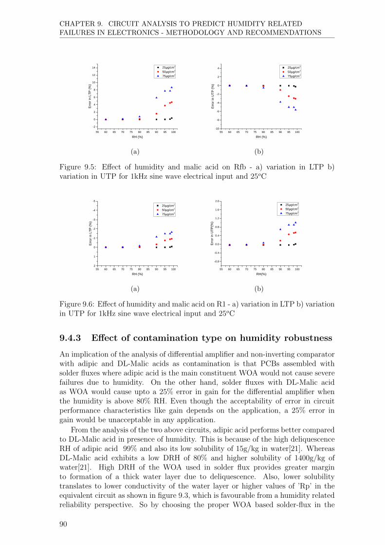
CHAPTER 9. CIRCUIT ANALYSIS TO PREDICT HUMIDITY RELATEDFAILURES IN ELECTRONICS - METHODOLOGY AND RECOMMENDATIONS
5 5 6 0 6 5 7 0 7 5 8 0 8 5 9 0 9 5 1 0 0- 2
0
2
4
6
8
1 0
1 2
1 4 2 5 µg / c m 2
5 0 µg / c m 2
7 5 µg / c m 2
Error
in LT
P (%)
R H ( % )
(a)
5 5 6 0 6 5 7 0 7 5 8 0 8 5 9 0 9 5 1 0 0- 1 0
- 8
- 6
- 4
- 2
0
2
4 2 5 µg / c m 2
5 0 µg / c m 2
7 5 µg / c m 2
Error
in UT
P (%)
R H ( % )
(b)
Figure 9.5: Effect of humidity and malic acid on Rfb - a) variation in LTP b)variation in UTP for 1kHz sine wave electrical input and 25oC
5 5 6 0 6 5 7 0 7 5 8 0 8 5 9 0 9 5 1 0 02
1
0
- 1
- 2
- 3
- 4
- 5 2 5 µg / c m 2
5 0 µg / c m 2
7 5 µg / c m 2
Error
in LT
P (%)
R H ( % )
(a)
5 5 6 0 6 5 7 0 7 5 8 0 8 5 9 0 9 5 1 0 0
- 0 . 8
- 0 . 4
0 . 0
0 . 4
0 . 8
1 . 2
1 . 6
2 . 0 2 5 µg / c m 2
5 0 µg / c m 2
7 5 µg / c m 2Err
or in
UTP(%
)
R H ( % )
(b)
Figure 9.6: Effect of humidity and malic acid on R1 - a) variation in LTP b) variationin UTP for 1kHz sine wave electrical input and 25oC
9.4.3 Effect of contamination type on humidity robustness
An implication of the analysis of differential amplifier and non-inverting comparatorwith adipic and DL-Malic acids as contamination is that PCBs assembled withsolder fluxes where adipic acid is the main constituent WOA would not cause severefailures due to humidity. On the other hand, solder fluxes with DL-Malic acidas WOA would cause upto a 25% error in gain for the differential amplifier whenthe humidity is above 80% RH. Even though the acceptability of error in circuitperformance characteristics like gain depends on the application, a 25% error ingain would be unacceptable in any application.
From the analysis of the two above circuits, adipic acid performs better comparedto DL-Malic acid in presence of humidity. This is because of the high deliquescenceRH of adipic acid 99% and also its low solubility of 15g/kg in water[21]. WhereasDL-Malic acid exhibits a low DRH of 80% and higher solubility of 1400g/kg ofwater[21]. High DRH of the WOA used in solder flux provides greater marginto formation of a thick water layer due to deliquescence. Also, lower solubilitytranslates to lower conductivity of the water layer or higher values of ’Rp’ in theequivalent circuit as shown in figure 9.3, which is favourable from a humidity relatedreliability perspective. So by choosing the proper WOA based solder-flux in the
90

CHAPTER 9. CIRCUIT ANALYSIS TO PREDICT HUMIDITY RELATEDFAILURES IN ELECTRONICS - METHODOLOGY AND RECOMMENDATIONS
5 5 6 0 6 5 7 0 7 5 8 0 8 5 9 0 9 5 1 0 00 . 2 0
0 . 1 5
0 . 1 0
0 . 0 5
0 . 0 0
- 0 . 0 5
- 0 . 1 0
- 0 . 1 5
- 0 . 2 0 2 5 u g / c m 2 5 0 u g / c m 2 7 5 u g / c m 2
Error
in LT
P (%)
R H ( % )
(a)
5 5 6 0 6 5 7 0 7 5 8 0 8 5 9 0 9 5 1 0 00 . 2 0
0 . 1 5
0 . 1 0
0 . 0 5
0 . 0 0
- 0 . 0 5
- 0 . 1 0
- 0 . 1 5
- 0 . 2 0 2 5 u g / c m 2 5 0 u g / c m 2 7 5 u g / c m 2
Error
in UT
P (%)
R H ( % )
(b)
Figure 9.7: Effect of humidity and adipic acid on Rfb - a) variation in LTP b)variation in UTP for 1kHz sine wave electrical input and 25oC
5 5 6 0 6 5 7 0 7 5 8 0 8 5 9 0 9 5 1 0 0- 0 . 2 0
- 0 . 1 5
- 0 . 1 0
- 0 . 0 5
0 . 0 0
0 . 0 5
0 . 1 0
0 . 1 5
0 . 2 02 5 u g / c m 25 0 u g / c m 27 5 u g / c m 2
Error
in LT
P (%)
R H ( % )
(a)
5 0 5 5 6 0 6 5 7 0 7 5 8 0 8 5 9 0 9 5 1 0 0- 0 . 2 0
- 0 . 1 5
- 0 . 1 0
- 0 . 0 5
0 . 0 0
0 . 0 5
0 . 1 0
0 . 1 5
0 . 2 0 2 5 u g / c m 2 5 0 u g / c m 2 7 5 u g / c m 2
Error
in UT
P (%)
R H ( % )
(b)
Figure 9.8: Effect of humidity and adipic acid on R1 - a) variation in LTP b)variation in UTP for 1kHz sine wave electrical input and 25oC
component assembly process the effects of humidity could be minimised to a greatextent.
The methodology demonstrated in this paper to simulate humidity and contam-ination related effects on electronics used leakage-current data where a single WOAwas the surface contamination. But, commercially available solder fluxes have mul-tiple WOAs as activators. Solder fluxes also contain vehicle, solvent and additivecomponents[28] which may have an effect on the formation of water layer on PCBs.More research can be done to study the correlation between data from single andmultiple WOA and also the data from actual commercially available solder fluxes.The leakage-current/SIR data could be implemented as a library in circuit simula-tors to simulate the effects of humidity and contamination.
Another way to minimise the effects of humidity and contamination is to incor-porate modifications in the cirucit design itself so that the circuit becomes morefault-tolerant. The following section demonstrate based on the above analysis, howone could improve the humidity robustness by modification of circuits.
91

CHAPTER 9. CIRCUIT ANALYSIS TO PREDICT HUMIDITY RELATEDFAILURES IN ELECTRONICS - METHODOLOGY AND RECOMMENDATIONS
9.5 Improvements to circuit reliability due to hu-
midity
An instrumentation amplifier is a modified version of the differential amplifier withbetter characteristics like higher input impedance and lower output impedance. Fig-ure 9.9a shows an instrumentation amplifier of gain 10 designed with opamps. Thegain ‘G’ of the instrumentation amplifier in figure 9.9a is given by:
G = (R2/R1) · (1 + 2 ·R6/R5) (9.3)
The instrumentation amplifier uses more components compared to a differentialamplifier with the advantage of better input and output impedances.
Similar to a non-inverting comparator, an inverting comparator is also used todetect a specific level on a sensed signal like temperature, pressure current, voltageetc. But unlike the non-inverting comparator, for an inverting comparator, outputof the comparator is a logic-low when input is above the UTP and a logic-high whenbelow LTP. Figure 9.10a shows an inverting comparator configuration.
The following subsections compares the functionalities of instrumentation ampli-fier with the differential amplier and inverting with non-inverting comparator. Alsoanalysed is the effect of splitting a high-value resistor into multiple resistances andrelated humidity responses.
9.5.1 Instrumentation amplifier vs differential amplifier
To relate the performances of differential and instrumentation amplifiers in the pres-ence of humidity and contamination, the errors in gain of both the circuits werecompared when humidity and contamination affects the resistances R1 and R6 ofdifferential and instrumentaion amplifiers respectively. The simulated contaminationwas DL-Malic acid at a surface concentration of 75ug/cm2. The same 0.1V, 1kHzsine signal applied for differential amplifier is used as the input also for this circuit.Figure 9.9b shows the comparison of the two circuits, which indicate that the errorin gain was similar for both the amplifiers until 80% RH which is the deliquescentRH for malic acid. For RH greater than 80%, instrumentation amplifier shows muchless error in gain compared to the differential amplifier. The maximum error shownby instrumentation amplifier was only 6% whereas for differential amplifier this wasnear to 25%. This shows that an instrumentation amplifier has higher reliabilityto humidity and hygroscopic contamination compared to differential amplifier. Theinstrumentation uses lower value components compared to the differential amplifierto achieve the same value of gain. Effect of humidity on a smaller value resistoris less compared to that of a bigger value resistor due to the formation of parallelequivalent of Rp with the resistor concerned. Also, since the gain determining pa-rameters are distributed among higher number of resistances for an instrumentationamplifier probability of water film formation on all the resistors at the same timealso decreases. Lower value resistances combined with the topology results in betterrobustness of instrumentation amplifier compared to the differential amplifier.
But, this improvement in reliability would come at an expense of higher compo-nent count. The instrumentation amplifier uses 3 opamps and 7 resistors whereasa differential amplifier uses only 1 opamp and 4 resistors. Hence, the choice to
92

CHAPTER 9. CIRCUIT ANALYSIS TO PREDICT HUMIDITY RELATEDFAILURES IN ELECTRONICS - METHODOLOGY AND RECOMMENDATIONS
+
-
OUT
+
-
OUT
+
-
OUT
Vin+
Vin-
Vout
R6
45k
R7
45k
R1
10k
R2
10k
R3
10k
R4
10k
R5
10k
(a)
5 5 6 0 6 5 7 0 7 5 8 0 8 5 9 0 9 5 1 0 0- 5
0
5
1 0
1 5
2 0
2 5
3 0 D i f f e r e n t i a l a m p l i f i e r I n s t r u m e n t a t i o n a m p l i f i e r
Abso
lute g
ain er
ror (%
)
R H ( % )
(b)
Figure 9.9: Comparison of differential and instrumentation amplifiers for effect ofhumidity - a) Schematic of Instrumentaion amplifier b) Variation in gains of differ-ential and instrumentation amplifiers with 0.1V, 1kHz sine wave electrical input and25oC
use either a differential or instrumentation amplifier would be based on a trade-offbetween the degradation in circuit performance and PCB space usage.
9.5.2 Inverting comparator vs Non-inverting comparator cir-cuit
When the non-inverting comparator of figure 9.2b is used for detecting over-currentsfor circuit protection applications, the 10% error in LTP during humidity exposureis definitely not acceptable and suitable solutions need to be found to lower the vul-nerability of the circuit to humidity-related effects. The inverting comparator couldbe a suitable alternative to the non-inverting comparator. A comparison is donebetween the non-inverting type of comparator to the inverting type of comparator.An inverting comparator is designed with the same threshold values as that of thenon-inverting comparator. Figure 9.10b compares both the circuits for their LTPwhen DL-Malic acid at 75µg/cm2 is used as the contamination affecting resistorRfb in both circuits. Negligible difference was noticed in the effect of humidity andcontamination on UTP of both comparator configurations.
Figure 9.10b showed that inverting comparator performs slightly better withlower error in LTP of 6% compared to 10% for non-inverting comparator. The errorin UTP was similar for both circuits. This improvement in performance with aninverting comparator could be beneficial depending on the application. Since samevalue components were used for both inverting and non-inverting comparators, thehigher robustness of the inverting configuration is solely due to the difference in thecircuit topology.
9.5.3 Higher humidity robustness by splitting high resis-tances
From the analysis of the differential amplifier, it was seen that the most sensitivecomponent was R1. Therefore one solution for improving humditiy robustness isto reduce the sensitivity of the resister for parasitic water film formation acting
93
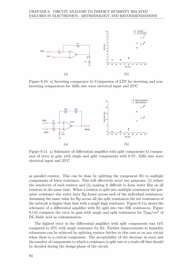
CHAPTER 9. CIRCUIT ANALYSIS TO PREDICT HUMIDITY RELATEDFAILURES IN ELECTRONICS - METHODOLOGY AND RECOMMENDATIONS
5Vdc
Rp1k
R1
20k
Rf b
100k
+
-
OUT
Vin
Vref
(a)
5 5 6 0 6 5 7 0 7 5 8 0 8 5 9 0 9 5 1 0 0- 10123456789
1 0 I n v e r t i n g N o n - i n v e r t i n g
Error
(%)
R H ( % )
(b)
Figure 9.10: a) Inverting comparator b) Comparison of LTP for inverting and non-inverting comparators for 1kHz sine wave electrical input and 25oC
R3
10k
R1a
50k
R4
100k
R1b
50k
OPAMP
+
-
OUT
R2
10k
Vin+
Vin-
Vout
(a)
5 5 6 0 6 5 7 0 7 5 8 0 8 5 9 0 9 5 1 0 00
5
1 0
1 5
2 0
2 5 S i n g l e c o m p o n e n t S p l i t c o m p o n e n t
Gain
error
(%)
R H ( % )
(b)
Figure 9.11: a) Schematic of differential amplifier with split components b) compar-ison of error in gain with single and split components with 0.1V, 1kHz sine waveelectrical input and 25oC.
as parallel resistor. This can be done by splitting the component R1 to multiplecomponents of lower resistance. This will effectively serve two purposes: (i) reducethe sensitivity of each resistor and (ii) making it difficult to form water film on allresistors at the same time. When a resistor is split into multiple resistances the par-asitic resistance due water layer Rp forms across each of the individual resistances.Assuming the same value for Rp across all the split resistances the net resistances ofthe network is higher than that with a single high resistance. Figure 9.11a shows theschematic of a differential amplifier with R1 split into two 50K resistances. Figure9.11b compares the error in gain with single and split resistances for 75µg/cm2 ofDL-Malic acid as contamination.
The highest error in the differential amplifier with split components was 14%compared to 25% with single resistance for R1. Further improvements in humidityrobustness can be achieved by splitting resistor further in this case or on any circuitwhen there is a critical component. The acceptability of the decrease in error andthe number of components to which a resistance is split into is a trade-off that shouldbe decided during the design-phase of the circuit.
94

CHAPTER 9. CIRCUIT ANALYSIS TO PREDICT HUMIDITY RELATEDFAILURES IN ELECTRONICS - METHODOLOGY AND RECOMMENDATIONS
9.6 Summary
This work has demonstrated simulation of robustness degradation of electronic cir-cuits due to humidity and surface contamination using experimental leakage-currentdata. The leakage-current data extracted was for two WOAs which are used as acti-vators in the no-clean flux systems namely - adipic and DL-Malic acid on a standardSIR pattern. The reliability of the circuits analysed decreased with increasing RHand decreased rapidly beyond DRH of the WOA used in the solder flux. The re-liability of electronic circuits to humidity and contamination can be significantlyimproved by the right choice of solder flux and the circuit configuration. A simula-tion of the effect of using various solder fluxes on circuits can be done in the designphase of the product itself by using the methodology presented here. The simulationcan help in choosing the right solder flux and make suitable circuit modificationsto improve reliability. If the reliability target cannot be met by the above, thenaccumulation of high humidity itself should be prevented by humidity control tech-niques or by use of conformal coatings. The methodology demonstrated in this workcan be incorporated into circuit simulation software packages to predict reliabilityof electronic circuits towards humidity and contamination in the design phase of theproduct itself.
9.7 Acknowledgement
This research was conducted as part of the IN SPE project funded by InnovationFund Denmark and CELCORR(www.celcorr.com). The authors would like to ac-knowledge the funding and help received from the consortium partners.
95

Bibliography
[1] V. Smet, F. Forest, J. Huselstein, F. Richardeau, Z. Khatir, S. Lefebvre, M.Berkani, ”Ageing and failure modes of IGBT modules in high temperaturepower cycling”, IEEE Trans. Ind. Elec., vol. 58, no. 10, pp. 4931-4941, October2011.
[2] R. M. Nelms et al. ”200C operation of a 500 W dc-dc converter utilizing powerMOSFETs,” IEEE Trans. Industry Applications, Vol. 33, No. 5, pp. 1267-1272,Sept./Oct. 1997.
[3] S. J. Krumbein, ”Metallic Electromigration Phenomena”, IEEE CHMT, pp. 5,March 1988.
[4] R. Hienonen, R. Lahtinen, Corrosion and climatic effects in electronics, VTTPublications, 2000.
[5] C. Hillman, J. Arnold, S. Binfield, and J. Seppi, “Silver and Sulfur: Case Stud-ies, Physics, and Possible Solutions,” SMTA International Conference, 2007.
[6] D. Minzari, M. S. Jellesen, P. Moller and R. Ambat, ”Morphological study ofsilver corrosion in highly aggressive sulfur environments,” Engineering failureanalysis, vol. 18, Issue 8, pp. 2126 – 2136, 2011.
[7] M. Tencer, ”Deposition of aerosol (”hygroscopic dust”) on electronics – Mecha-nism and risk,” Microelectronics reliability, vol. 48, Issue 8, pp. 584–593, 2008.
[8] R. B. Comizzoli, R. P. Frankenthal, P. C. Milner, J. D. Sinclair,”Corrosion ofElectronic Materials and Devices”, Science, Vol. 234, no. 4774 , pp. 340-345,1986
[9] J. D. Sinclair, L. A. Psota-Kelty, C. J. Weschler and H. C. Shields, ” Depositionof Airborne Sulfate, Nitrate, and Chloride Salts as It Relates to Corrosion ofElectronics,” Journal of electrochemical society, Vol. 137, Issue 4, pp. 1200–1206, 1990.
[10] H. Conseil-Gudla, Z. Staliulionis, M. S. Jellesen, M. Jabbari, J. H. Hattel,R. Ambat, ” Humidity build-up in electronic enclosures exposed to constantconditions,” IEEE transactions on components packaging and manufacturingtechnology, vol.7, Issue 3, pp. 412–423, 2017.
[11] H. Conseil, V. C. Gudla, M. S. Jellesen, R. Ambat, Humidity build-up in atypical electronic enclosure exposed to cycling conditions and effect on corrosionreliability, IEEE Transactions on Components, Packaging and ManufacturingTechnology, vol. 6, Issue 9, pp. 1379–1388, 2016.
96

BIBLIOGRAPHY
[12] A. W. Adamson, A. P. Gast, Physical chemistry of surfaces, John wiley andsons Inc., 1997.
[13] M. Tencer, Moisture Ingress into Nonhermetic Enclosures and Packages.AQuasi-Steady State Model for Diffusion and Attenuation of Ambient Humid-ity Variations, Electronic components and technology conference, pp. 196–209,1994.
[14] J. B. Jacobsen, J. P. Krog, A. H. Holm, L. Rimestad, A. Riis, Climate-Protective Packaging Using Basic Physics to Solve Climatic Challenges for Elec-tronics in Demanding Applications, IEEE Industrial Electronics Magazine, vol.8, Issue 3, pp. 51–59, 2014.
[15] D. Minzari, M. S. Jellesen, P. Moller and R. Ambat, ” On the electrochemicalmigration of tin in electronics,” Corrosion science, Vol. 53, Issue 10, pp. 3366–3379, 2011.
[16] H. Conseil, M. S. Jellesen and R. Ambat, ” Printed Circuit Board SurfaceFinish and Effects of Chloride Contamination, Electric Field, and Humidityon Corrosion Reliability,” Journal of electronic materials, Vol. 46, Issue 2, pp.817–825, 2017.
[17] B.I. Noh, S.B. Jung, ”Characteristics of environmental factor for electrochemi-cal migration on printed circuit board”, Journal of Materials Science: Materialsin Electronics, Vol. 19, Issue 10, pp. 952-–956, 2008.
[18] D.Q. Yu, W. Jillek, E. Schmitt, ”Electrochemical migration of lead free solderjoints”, Journal of Materials Science: Materials in Electronics, Vol. 17, Issue 3,pp 229-–241, 2006.
[19] D. Pauls, “Residues in printed wiring boards and assemblies,” Circuit World,vol. 27, no. 1, pp. 32–41, Oct. 2000.
[20] H. Conseil, M. S. Jellesen and R. Ambat, ” Contamination profile of PrintedCircuit Board Assemblies in relation to soldering types and conformal coating,”Proceedings of Eurocorr 2014, 2014.
[21] V. Verdingovas, M. S. Jellesen and R. Ambat, ”Solder Flux Residues andHumidity-Related Failures in Electronics: Relative Effects of Weak OrganicAcids Used in No-Clean Flux Systems,” Journal of Electronic Materials, Vol.44, Issue 4, pp. 1116–1127, 2015.
[22] S. Zhan, M. H. Azarian, M. Pecht, ”Surface Insulation Resistance of Confor-mally Coated Printed Circuit Boards Processed with No-Clean Flux”, IEEETransactions on Electronics Packaging Manufacturing, vol. 29, no. 3, pp. 217-223, July 2006.
[23] L. C. Zou; C. Hunt, ”Characterization of the Conduction Mechanisms in Ad-sorbed Electrolyte Layers on Electronic Boards Using AC Impedance,” Journalof the Electrochemical Society, Vol. 156, Issue 1, pp. C8–C15, 2009.
97

BIBLIOGRAPHY
[24] V. Verdingovas, M. S. Jellesen and R. Ambat, ”Relative effect of solder fluxchemistry on the humidity related failures in electronics,” Soldering and SurfaceMount Technology, Vol. 27, Issue 4, pp. 146–156, 2015.
[25] V. Verdingovas, S. Joshy, M. S. Jellesen, R. Ambat, ”Analysis of surface in-sulation resistance related failures in electronics by circuit simulation,” CircuitWorld, Vol. 43, Issue 2, pp. 45–55, 2017.
[26] S. Joshy, V. Verdingovas, M. Jellesen, R. Ambat, ”Simulation of electroniccircuit sensitivity towards humidity using electrochemical data on water layer”,proceeding in 17th Electronics Packaging Technology Conference (EPTC), pp.1-5, 2015.
[27] V. Verdingovas, M. S. Jellesen, R Ambat, ”Impact of NaC1 Contamination andClimatic Conditions on the Reliability of Printed Circuit Board Assemblies”,IEEE Transactions on Device and Materials Reliability, vol. 14, no. 1, pp. 42-51,2014.
[28] M.S. Jellesen, D. Minzari, U. Rathinavelu, P. Moller, R. Ambat, ” Corrosionfailure due to flux residues in an electronic add-on device”, Engineering failureanalysis”, Vol. 17, Issue 6, pp. 1263-1272, 2010.
98
Chapter 10
Overall discussion
This chapter contains an overall discussion of the investigations presented in the pa-pers. The results have shown possibility to control humidity and prevent humidityfailures inside electronic enclosures by preferential condensation and internal heatingmethods. The results have also shown the main enclosure packaging related factorsand their contribution to humidity accumulation and humidity profiles in electronicenclosures. The circuit simulation methodology was used to predict humidity re-lated failures in electronic circuits and was also used to find more reliable circuittopologies.
Study of humidity transfer from warm to cold showed that high humidity insidean electronic enclosure can be lowered by mass transfer to a condensing surface,hence showing the feasibility of using forced condensation for humidity control. Thecondensing surface required to bring about humidity transfer and hence humiditycontrol can be realised by using thermoelectric coolers (TEC). A condensing surfacecould also exist in an enclosure due to the nature of the application, for examplea pump used to circulate cold water. The surfaces of the pump in contact withcold water could be condensing in nature and when interfaced with the enclosureof the pump control electronics through suitable opening, could control any highhumidity in the electronic enclosure. The main parameters that influenced masstransfer to the condensing surface were warm temperature, cold surface temperature,connecting hole between the warm and cold sections and enclosure openings whichcontrol humidity ingress from ambient. The effect of enclosure openings on humiditycontrol was investigated in chapter five. Lower humidity was achieved in the warmchamber by having a lower size for the warm chamber opening which limits theingress of humidity from ambient into the warm chamber. But, the adverse effectof using a smaller warm chamber opening was the slower transient response of thehumidity control mechanism. In a humidity control application using TECs to createa condensing surface, the cold surface temperature depends on the current throughthe TEC. A higher current would correspond to lower cold surface temperaturesand hence, lower RH. But, this would increase the power consumed for humiditycontrol, which is critical especially for battery powered applications. The values ofthe different opening sizes and cold surface temperature should be selected based onmaximum acceptable RH in the warm chamber, preferred transient response timesand also on the knowledge of the ambient climatic conditions.
Humidity accumulation was observed in an electronic enclosure with parallelplates subjected to cycling ambient temperature and internal heating leading to
99

CHAPTER 10. OVERALL DISCUSSION
impedance degradation and susceptibility to failures. Power dissipating PCBAs andcircuits in their near vicinity would be relatively safe from humidity related failuresdue to their higher surface temperatures from the heat dissipated. Componentsplaced on high heat capacity components like heat sinks would experience humidityrelated failures as demonstrated. So, critical components should be placed fartheraway from high heat capacity components to ensure their reliability. Another wayto improve reliability of PCBA in electronic enclosures would be to use controlledopenings with higher resistance to flows like tubes instead of holes. As compared tohumidity control by forced condensation, internal heating was able to prevent relia-bility degradation only on specific surfaces of PCBA and not in the entire enclosure.This is because forced condensation is an absolute humidity control method, wherethe absolute amount of humidity in the air is controlled where as, heating is a rela-tive humidity control method where the RH near critical surfaces are controlled toprevent condensation.
The simulation methodology using SIR data was used to analyse reliability ofcommonly used electronic circuits like a differential amplifier, instrumentation am-plifier, non-inverting and inverting comparators to humidity and contamination.The simulations were used to identify sensitive components in the circuit and alsoto select more reliable circuit topologies. This improvement in reliability could hap-pen at the expense of more number of components and hence, larger PCB area. Thesimulation methodology can be used as a tool in the design and analysis phase ofproduct development to choose reliable circuit topologies and to compare and selectsuitable solder flux for component assembly.
100
Chapter 11
Overall conclusion
1. Humidity transfer occurred from warm chamber to cold chamber. The mainfactors that influenced the humidity transfer were temperature of the warmchamber, cold chamber temperature and connecting hole size.
2. Humidity control by forced condensation was demonstrated using a two-chamberset-up. Forced condensation reduced the RH inside both chambers of the set-up. This showed a humidity control method for an electronic enclosure capableof exchanging humidity to a condensing surface.
3. Humidity control by forced condensation was found to be influenced by coldsurface temperature and enclosure opening sizes. Lower cold surface tem-perature caused lower RH in both chambers. Effect of larger warm chamberopening and connecting hole sizes were to increase the steady state RH insidethe warm chamber where as, a larger cold chamber opening sizes led lower RHvalues.
4. Cycling ambient temperature and internal heat dissipation was shown to causehumidity accumulation inside electronic enclosures. Internal heating resultedin release of adsorbed water vapour which condensed on cooler surfaces, in-creasing the susceptibility to humidity related failures on those surfaces.
5. Humidity control by internal heating was demonstrated in an enclosure withsimulated parallel PCBs. Reliability improvement due to the heating wasfound to be feasible only on directly heated PCBA surfaces and PCBA placedin close proximity to the heat source.
6. Circuits located near high heat capacity components would experience impedancedegradation and humidity related failures due to higher time constants for tem-perature, leading to low peak to peak temperatures and RH in their vicinity.
7. Larger enclosure opening size caused higher impedance degradation and sus-ceptiblity to humidity related failures. Enclosure openings like tubes havehigher resistance to flow leading to slower accumulation of humidity inside theenclosure, and hence should be preferred as controlled openings on electronicenclosures.
8. The simulation methodology using SIR data was used to analyse common elec-tronic circuits. Components in the circuits causing higher error in presence
101

CHAPTER 11. OVERALL CONCLUSION
of humidity and contamination were identified using the simulation method-ology. Circuits with better reliability to humidity were suggested. Also, effectof different WOAs on circuit performance in the presence of humidity wasanalysed.
Suggestions for future work
Condensation based humidity control could be implemented in an electronic enclo-sure using thermoelectric coolers(TEC) to study both continuous and pulsed opera-tions. Energy required to be spent for humidity control by condensation could alsobe investigated.
High heat capacity components could be used to store heat dissipated by elec-tronic components during operation and later used to keep critical components warmcan be explored. Experiments can be conducted to investigate the feasibility of us-ing phase change materials to store a part of the generated heat, which can be usedlater to keep the PCBA warm during the off time of the heater. Use of Resistor-capacitor(RC) networks to model accumulation of humidity inside electronic enclo-sures both by diffusion and convection could be investigated as an alternative tocomputationally intensive CFD models.
The methodology to predict humidity related failures can be implemented aspart of a circuit simulation tool to analyse reliability of circuits under conditions ofhumidity and contamination. This would also help to compare different flux systemsand choose the most reliable flux system to be used in component assembly.
102


This PhD work was motivated by the need to improve the reliability of electronics
to humidity related failures by understanding humidity build-up inside electronic
enclosures and study suitable humidity control techniques. In the industry, reliabil-
ity to humidity related failures is taken care with experience generated over many
years of product development. This work aims to contribute to the scientific under-
standing of humidity build-up and humidity control inside electronic enclosures.
This work has studied the effect of enclosure packaging level parameters on hu-
midity build-up under conditions of cycling ambient temperature. Enclosure humid-
ity profiles under constant ambient conditions and condensed water was also stud-
ied. Humidity control techniques based on heating and preferential condensation
were investigated. Humidity transfer from warm to cold regions inside an enclosure
were studied with hermetically sealed glass enclosures. A methodology based on
electronic circuit analysis to predict humidity related failures and evaluate different
electronic circuits in the presence of humidity and contamination was also studied.
DTU Mechanical EngineeringSection of Materials and Surface EngineeringTechnical University of Denmark
Produktionstorvet, Bld. 425DK-2800 Kgs. Lyngby Denmark
Tlf.: +45 4525 2205Fax: +45 4525 1961
www.mek.dtu.dk
October 2018
ISBN: 978-87-7475-553-1