Homework #3 Solutionangelar/ECE3110Fa10_HW3sol.pdf8. Consider the basic bipolar differential circuit...
9
Fall 2010 1. In a particular cascaded current transistors have V t =0,6V, µ n C ox =160 W 1 =W 4 =4µm, and W 2 =W 3 =40µm. T output current results? What are th What is the lowest voltage at the ou possible? What are the values of g m resistance of the mirror? Homework #3 Solution mirror, such as that shown at the right, all 0µA/V 2 , L=1µm, and V A =10V. Widths The reference current I REF is 20µA. What he voltages at the gates of Q 2 and Q 3 ? utput for which current-source operation is m and r o of Q 2 and Q 3 ? What is the output 1
Transcript of Homework #3 Solutionangelar/ECE3110Fa10_HW3sol.pdf8. Consider the basic bipolar differential circuit...
Fall 2010
1. In a particular cascaded current
transistors have Vt=0,6V, µnCox=160
W1=W4=4µm, and W2=W3=40µm. The
output current results? What are the voltages at the gates of Q
What is the lowest voltage at the output for which current
possible? What are the values of gm
resistance of the mirror?
Homework #3 Solution
1. In a particular cascaded current mirror, such as that shown at the right, all
=160µA/V2, L=1µm, and VA=10V. Widths
µm. The reference current IREF is 20µA. What
output current results? What are the voltages at the gates of Q2 and Q3?
What is the lowest voltage at the output for which current-source operation is
m and ro of Q2 and Q3? What is the output
1

Fall 2010
2. Find the output resistance of the double
Homework #3 Solution
2. Find the output resistance of the double-cascode current mirror below.
2
Fall 2010
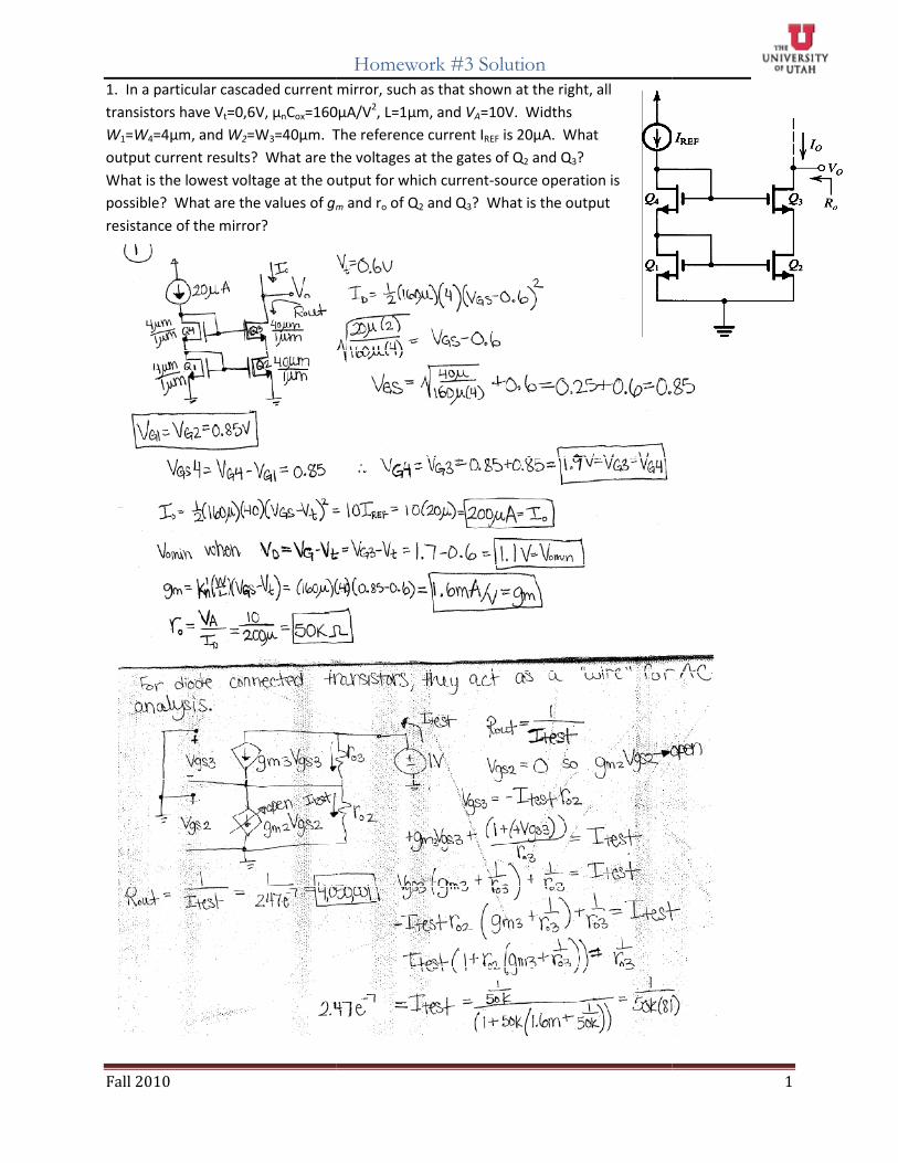
3. Show that the input resistance (R seen at V3 node
by 2/gm. Assume that all three transistors are identical and neglect the Early effect. (Hint: Use a test
source and find the Thevenin equivalent resistance)
Homework #3 Solution
R seen at V3 node) for the Wilson MOS mirror shown
. Assume that all three transistors are identical and neglect the Early effect. (Hint: Use a test
source and find the Thevenin equivalent resistance)
V3
3
) for the Wilson MOS mirror shown at right is given
. Assume that all three transistors are identical and neglect the Early effect. (Hint: Use a test
Fall 2010
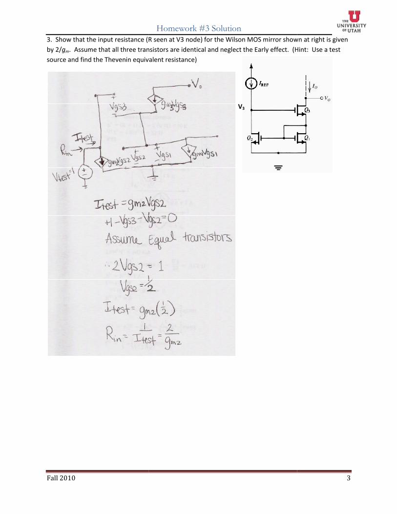
4. (a) For the circuit below, assume BJTs with high
result in Io=10µA.
(b) For the design in (a), find Ro assuming
Homework #3 Solution
For the circuit below, assume BJTs with high β and vBE=0.8V at 1mA. Find the value of R that will
assuming β=100 and VA=50V.
4
=0.8V at 1mA. Find the value of R that will
Fall 2010
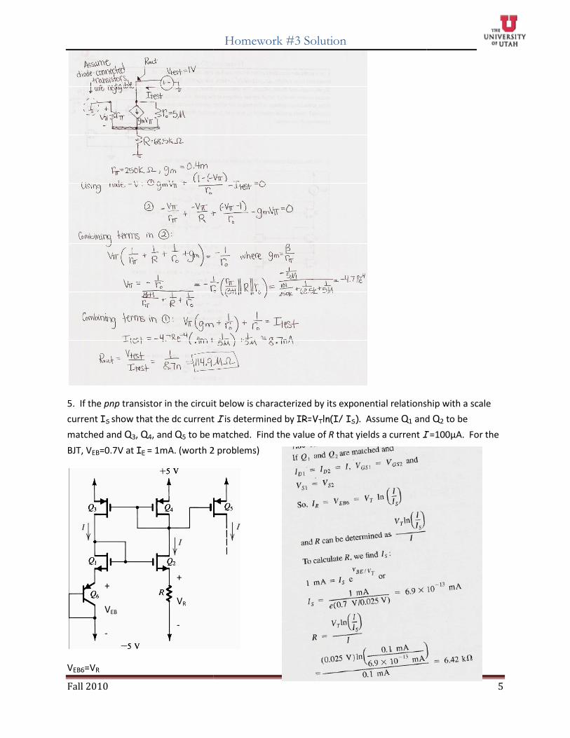
5. If the pnp transistor in the circuit below is characterized by its exponential relationship with a scale
current IS show that the dc current
matched and Q3, Q4, and Q5 to be matched. Find the value of
BJT, VEB=0.7V at IE = 1mA. (worth 2 problems)
VEB6=VR
+
VEB
-
+
VR
-
Homework #3 Solution
transistor in the circuit below is characterized by its exponential relationship with a scale
show that the dc current I is determined by IR=VTln(I/ IS). Assume Q1 and
to be matched. Find the value of R that yields a current I
(worth 2 problems)
5
transistor in the circuit below is characterized by its exponential relationship with a scale
and Q2 to be
I =100µA. For the
Fall 2010
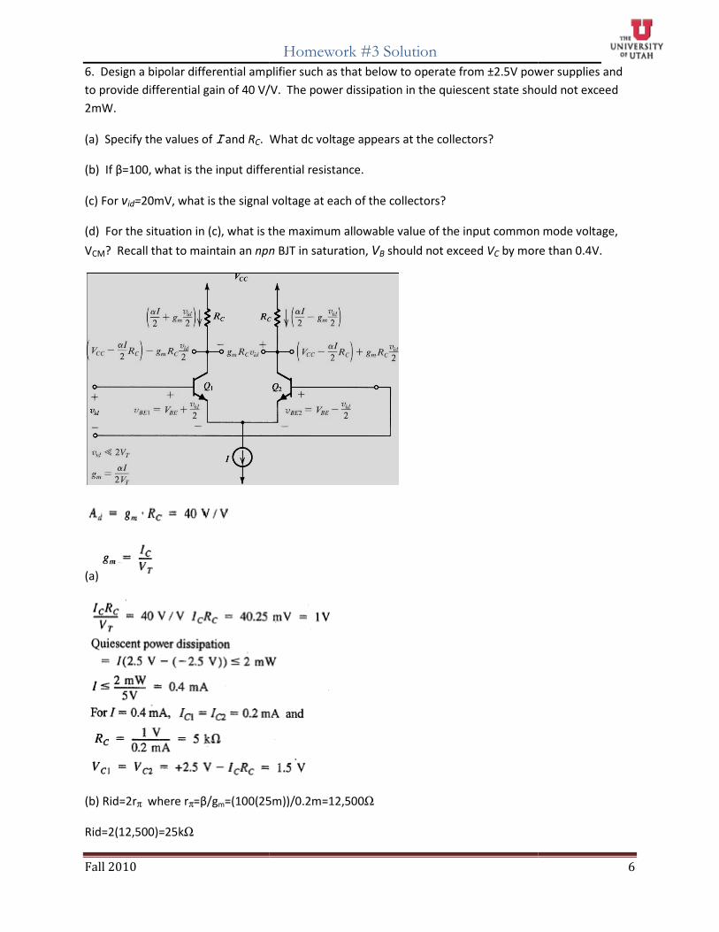
6. Design a bipolar differential amplifier such as that below to operate from
to provide differential gain of 40 V/V. The power
2mW.
(a) Specify the values of I and RC. What dc voltage appears at the collectors?
(b) If β=100, what is the input differential resistance.
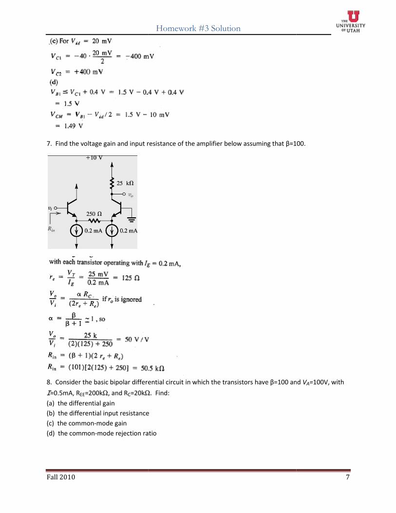
(c) For vid=20mV, what is the signal voltage at each of the
(d) For the situation in (c), what is the maximum allowable value of the input common mode voltage,
VCM? Recall that to maintain an npn
(a)
(b) Rid=2rπ where rπ=β/gm=(100(25m)
Rid=2(12,500)=25kΩ
Homework #3 Solution
6. Design a bipolar differential amplifier such as that below to operate from ±2.5V power supplies and
to provide differential gain of 40 V/V. The power dissipation in the quiescent state should not exceed
. What dc voltage appears at the collectors?
=100, what is the input differential resistance.
20mV, what is the signal voltage at each of the collectors?
(d) For the situation in (c), what is the maximum allowable value of the input common mode voltage,
npn BJT in saturation, VB should not exceed VC by more than 0.4V.
(25m))/0.2m=12,500Ω
6
2.5V power supplies and
dissipation in the quiescent state should not exceed
(d) For the situation in (c), what is the maximum allowable value of the input common mode voltage,
by more than 0.4V.
Fall 2010
7. Find the voltage gain and input resistance of the amplifier below assuming that
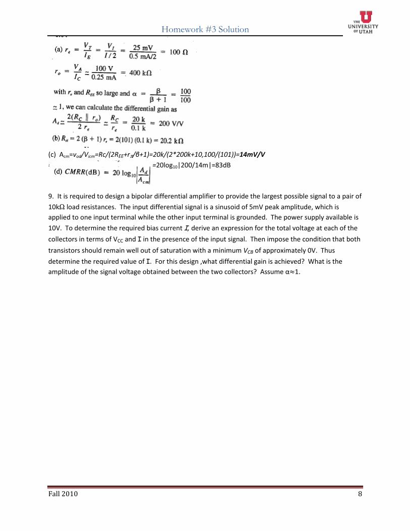
8. Consider the basic bipolar differential circuit in which the transistors have
I=0.5mA, REE=200kΩ, and RC=20kΩ
(a) the differential gain
(b) the differential input resistance
(c) the common-mode gain
(d) the common-mode rejection ratio
Homework #3 Solution
7. Find the voltage gain and input resistance of the amplifier below assuming that β=100.
8. Consider the basic bipolar differential circuit in which the transistors have β=100 and
Ω. Find:
(b) the differential input resistance
mode rejection ratio
7
=100.
=100 and VA=100V, with
Homework #3 Solution
Fall 2010 8
(c) Acm=vod/Vicm=Rc/(2REE+rπ/β+1)=20k/(2*200k+10,100/(101))=14mV/V
= =20log10|200/14m|=83dB
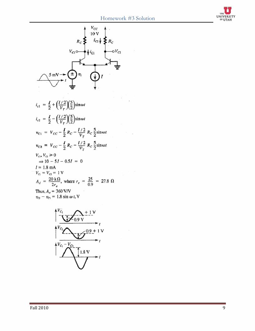
9. It is required to design a bipolar differential amplifier to provide the largest possible signal to a pair of
10kΩ load resistances. The input differential signal is a sinusoid of 5mV peak amplitude, which is
applied to one input terminal while the other input terminal is grounded. The power supply available is
10V. To determine the required bias current I, derive an expression for the total voltage at each of the
collectors in terms of VCC and I in the presence of the input signal. Then impose the condition that both
transistors should remain well out of saturation with a minimum VCB of approximately 0V. Thus
determine the required value of I. For this design ,what differential gain is achieved? What is the
amplitude of the signal voltage obtained between the two collectors? Assume α≈1.
Homework #3 Solution
Fall 2010 9


![Vision-Based Relative Navigation and Control for Autonomous … · American Institute of Aeronautics and Astronautics 3 with [ ] T m mx my mz ω = ω ω ω denoting the inspector](https://static.fdocuments.us/doc/165x107/5e7e173347cbfc4ede6f064a/vision-based-relative-navigation-and-control-for-autonomous-american-institute-of.jpg)


