Highly-crystalline 6 inch free-standing GaN observed using ...
6
CrystEngComm PAPER Cite this: CrystEngComm, 2021, 23, 1628 Received 28th October 2020, Accepted 17th December 2020 DOI: 10.1039/d0ce01572e rsc.li/crystengcomm Highly-crystalline 6 inch free-standing GaN observed using X-ray diffraction topography Jaemyung Kim, ab Okkyun Seo, abc L. S. R. Kumara, abc Toshihide Nabatame, a Yasuo Koide a and Osami Sakata * abcd We demonstrate the crystal quality of a 6 inch (0001) plane free-standing GaN substrate grown using a Na-flux based liquid phase epitaxy method. The 112 ¯4 rocking curve profiles of every point over the substrate were recorded by synchrotron X-ray diffraction topography. The reconstructed images show that there is a huge boundary between the high crystalline area and the low crystalline area in the substrate. Anisotropic bowing of the lattice planes with respect to the [101 ¯0] direction was obtained from wafer bending analysis. The mean width of the rocking curves over the wafer was 0.024°, which indicates that the newly fabricated 6 inch GaN substrate was almost a single crystal. We found that there was a competition between crystallinity and homogeneity. Introduction The growth of large scale GaN is important for the mass production of optoelectronic devices 1,2 and power devices. 3,4 In commercially available LEDs (light-emitting diodes) or GaN HEMT (high-electron mobility transistors), GaN films are grown on foreign materials such as SiC (ref. 5 and 6) and sapphire. 7,8 However, because of the significant lattice mismatch between GaN and its growth substrates, threading dislocation occurs and deteriorates device performance and lifetime. 9,10 Although buffer layers such as InGaN can be used between the substrate and GaN, 11–14 lattice mismatch still occurs, and dislocation densities are still high. Despite significant progress in crystal growth techniques, dislocations are easily observed in GaN-based devices. In the case of a GaN laser diode, Mg-related point defects diffuse to the active layer through threading dislocation that degrades the lifetime of the device. 9 It has been observed that a high dislocation density lowers drain current and the transconductance peak value and degrades the frequency response in GaN HEMT power devices. 10 Accordingly, lowering the dislocation density is essential to increase device reliability and performance. A drastic lowering of the dislocation density can be achieved by employing a GaN bulk instead of a thin film. A thick GaN boule is grown on top of a foreign substrate such as SiC, 15 sapphire, 16–18 and GaAs (ref. 19) with GaN seeds or various patterns. In the case of the seed-based method, the GaN seeds undergo ELO (epitaxial lateral overgrowth), forming a thick single-crystalline GaN boule. 20 Free-standing GaN crystals have been obtained by separating the GaN boule from the foreign sacrificial layer using a laser lift-off process. 21 However, because of the difficulty in controlling the growth rate while preserving morphological stability, it is still challenging to increase the substrate size. 22 For the growth of the bulk GaN substrate, HVPE (hydride vapor phase epitaxy), 23,24 ammonothermal methods, 25 Li-flux based methods, 26,27 and Na-flux based methods 28–34 have been widely used. Among the methods, the Na-flux based LPE (liquid phase epitaxy) method has attracted attention due to its low growth temperature. There have been many trials to increase GaN substrate size since 1996, when the first free-standing GaN crystals were obtained (around 5 mm in size). 22 After one year, the crystal size had increased to 10 mm by growing crystals for 200 hours, 22 and by 1998, the crystal size had increased up to 15 mm. 22 The technology became commercially viable after the development of 2 inch free-standing GaN. Since that time, the wafer size increased up to 6 inch in 2018; 24 however, the wafer was not characterized. According to a recent report on 4 inch free-standing GaN grown using an HVPE method, 35 the mean crystallinity over the substrate was high, showing narrow X-ray rocking curves over the substrate. The radius of curvature reached 35 m, and the mean FWHM of the GaN 112 ¯ 4 was 33 arcsecs, which 1628 | CrystEngComm, 2021, 23, 1628–1633 This journal is © The Royal Society of Chemistry 2021 a Center for GaN Characterization and Analysis, Research Network and Facility Services Division (RNFS), National Institute for Materials Science (NIMS), Tsukuba, Ibaraki, 305-0047, Japan. E-mail: [email protected] b Synchrotron X-ray Station at SPring-8, RNFS, NIMS, Kouto, Sayo, Hyogo 679- 5148, Japan c Synchrotron X-ray Group, Research Center for Advanced Measurement and Characterization, NIMS, Kouto, Sayo, Hyogo 679-5148, Japan d Center for Synchrotron Radiation Research Institute (JASRI), Kouto, Sayo, Hyogo 679-5198, Japan Open Access Article. Published on 01 February 2021. Downloaded on 11/17/2021 10:47:18 AM. This article is licensed under a Creative Commons Attribution-NonCommercial 3.0 Unported Licence. View Article Online View Journal | View Issue
Transcript of Highly-crystalline 6 inch free-standing GaN observed using ...

CrystEngComm
PAPER
Cite this: CrystEngComm, 2021, 23,
1628
Received 28th October 2020,Accepted 17th December 2020
DOI: 10.1039/d0ce01572e
rsc.li/crystengcomm
Highly-crystalline 6 inch free-standing GaNobserved using X-ray diffraction topography
Jaemyung Kim,ab Okkyun Seo,abc L. S. R. Kumara,abc Toshihide Nabatame,a
Yasuo Koidea and Osami Sakata *abcd
We demonstrate the crystal quality of a 6 inch (0001) plane free-standing GaN substrate grown using a
Na-flux based liquid phase epitaxy method. The 112̄4 rocking curve profiles of every point over the
substrate were recorded by synchrotron X-ray diffraction topography. The reconstructed images show that
there is a huge boundary between the high crystalline area and the low crystalline area in the substrate.
Anisotropic bowing of the lattice planes with respect to the [101̄0] direction was obtained from wafer
bending analysis. The mean width of the rocking curves over the wafer was 0.024°, which indicates that
the newly fabricated 6 inch GaN substrate was almost a single crystal. We found that there was a
competition between crystallinity and homogeneity.
Introduction
The growth of large scale GaN is important for the massproduction of optoelectronic devices1,2 and power devices.3,4
In commercially available LEDs (light-emitting diodes) or GaNHEMT (high-electron mobility transistors), GaN films aregrown on foreign materials such as SiC (ref. 5 and 6) andsapphire.7,8 However, because of the significant latticemismatch between GaN and its growth substrates, threadingdislocation occurs and deteriorates device performance andlifetime.9,10 Although buffer layers such as InGaN can be usedbetween the substrate and GaN,11–14 lattice mismatch stilloccurs, and dislocation densities are still high.
Despite significant progress in crystal growth techniques,dislocations are easily observed in GaN-based devices. In thecase of a GaN laser diode, Mg-related point defects diffuse tothe active layer through threading dislocation that degradesthe lifetime of the device.9 It has been observed that ahigh dislocation density lowers drain current and thetransconductance peak value and degrades the frequencyresponse in GaN HEMT power devices.10 Accordingly,lowering the dislocation density is essential to increasedevice reliability and performance.
A drastic lowering of the dislocation density can beachieved by employing a GaN bulk instead of a thin film. Athick GaN boule is grown on top of a foreign substrate suchas SiC,15 sapphire,16–18 and GaAs (ref. 19) with GaN seeds orvarious patterns. In the case of the seed-based method, theGaN seeds undergo ELO (epitaxial lateral overgrowth),forming a thick single-crystalline GaN boule.20 Free-standingGaN crystals have been obtained by separating the GaN boulefrom the foreign sacrificial layer using a laser lift-offprocess.21 However, because of the difficulty in controllingthe growth rate while preserving morphological stability, it isstill challenging to increase the substrate size.22 For thegrowth of the bulk GaN substrate, HVPE (hydride vaporphase epitaxy),23,24 ammonothermal methods,25 Li-flux basedmethods,26,27 and Na-flux based methods28–34 have beenwidely used. Among the methods, the Na-flux based LPE(liquid phase epitaxy) method has attracted attention due toits low growth temperature.
There have been many trials to increase GaN substratesize since 1996, when the first free-standing GaN crystalswere obtained (around 5 mm in size).22 After one year, thecrystal size had increased to 10 mm by growing crystals for200 hours,22 and by 1998, the crystal size had increased up to15 mm.22 The technology became commercially viable afterthe development of 2 inch free-standing GaN. Since thattime, the wafer size increased up to 6 inch in 2018;24
however, the wafer was not characterized.According to a recent report on 4 inch free-standing GaN
grown using an HVPE method,35 the mean crystallinity overthe substrate was high, showing narrow X-ray rocking curvesover the substrate. The radius of curvature reached 35 m,and the mean FWHM of the GaN 112̄4 was 33 arcsecs, which
1628 | CrystEngComm, 2021, 23, 1628–1633 This journal is © The Royal Society of Chemistry 2021
a Center for GaN Characterization and Analysis, Research Network and Facility
Services Division (RNFS), National Institute for Materials Science (NIMS), Tsukuba,
Ibaraki, 305-0047, Japan. E-mail: [email protected] Synchrotron X-ray Station at SPring-8, RNFS, NIMS, Kouto, Sayo, Hyogo 679-
5148, Japanc Synchrotron X-ray Group, Research Center for Advanced Measurement and
Characterization, NIMS, Kouto, Sayo, Hyogo 679-5148, JapandCenter for Synchrotron Radiation Research Institute (JASRI), Kouto, Sayo, Hyogo
679-5198, Japan
Ope
n A
cces
s A
rtic
le. P
ublis
hed
on 0
1 Fe
brua
ry 2
021.
Dow
nloa
ded
on 1
1/17
/202
1 10
:47:
18 A
M.
Thi
s ar
ticle
is li
cens
ed u
nder
a C
reat
ive
Com
mon
s A
ttrib
utio
n-N
onC
omm
erci
al 3
.0 U
npor
ted
Lic
ence
.
View Article OnlineView Journal | View Issue
CrystEngComm, 2021, 23, 1628–1633 | 1629This journal is © The Royal Society of Chemistry 2021
shows an almost single-crystal behaviour. However, thecrystallinity of the substrate tended to decrease from thecentre to the edge, including lattice plane bowing. Moreover,there was inhomogeneity in the FWHM distribution over thesubstrate during crystal growth, which may be related to ahigh dislocation density originating from the GaN seeds. Thecrystallinity near the GaN seed was lower than that in otherplaces, which resulted in inhomogeneity.
Here, we present the synchrotron X-ray diffractioncharacterization results of 6 inch free-standing GaN grownusing a Na-flux based LPE method for the first time. Wediscuss the crystallinity and local lattice plane shape of thewhole wafer using X-ray diffraction topography combinedwith rocking curve imaging.
Experimental details
A 6 inch, n-type wurtzite GaN c-plane substrate was grownusing a Na-flux based LPE method. Both sides of thesubstrate were polished with a thickness of 0.4 mm. Duringthe wafer polishing, the off-cut angle was adjusted to 0.3°toward the [11-20] direction. X-ray diffraction topography wasperformed at BL20B2, SPring-8, Japan. A schematic view ofthe experimental configuration is illustrated in Fig. 1(a).
X-rays of 1.3 Å were selected using a Si(111) double crystalmonochromator (DCM). The X-ray beam size was adjusted tobe larger than 100 mm (h) × 3 mm (v). Because of thelimitation of the detection area of a flat panel detector(Hamamatsu, C7942CA-22), the 6 inch substrate wastranslated to almost perpendicular and parallel directionswith respect to the X-ray incident beam for full areaillumination. The detector was placed almost parallel to thesample surface with a sample-to-detector distance of 30 cm.The detector pixel size was 50 × 50 μm2, and the pixelnumbers were 2368 × 2240. The GaN 112̄4 diffraction wasselected for the topography. The 6 inch substrate was placedat the rotation centre by minimising tension. The interplanarangle between the GaN(0001) and (112̄4) is 39.16°, and the
Fig. 1 Experimental configuration for synchrotron X-ray diffractiontopography on the 6 inch free-standing GaN substrate is described in(a). X-rays of 1.3 Å selected using a Si(111) monochromator werediffracted by the GaN(112̄4) net planes at an angle of 2θB = 80.5°. Thediffraction signals were recorded at various incident angles θ. Thesnapshots of the diffracted images at the azimuth angles of ϕ = 0° andϕ = 120° are illustrated in (b) and (c), respectively. Due to the localanisotropic lattice plane bowing, the diffraction images are inclined, inthe case of ϕ = 120°.
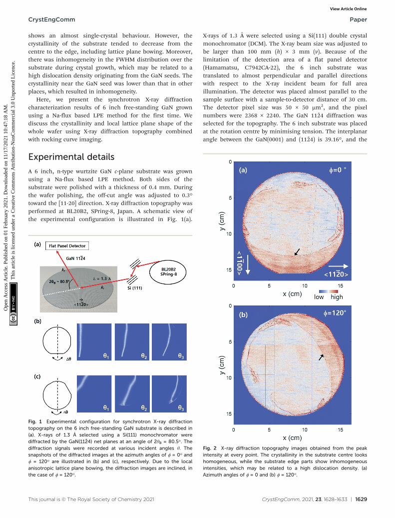
Fig. 2 X-ray diffraction topography images obtained from the peakintensity at every point. The crystallinity in the substrate centre lookshomogeneous, while the substrate edge parts show inhomogeneousintensities, which may be related to a high dislocation density. (a)Azimuth angles of ϕ = 0 and (b) ϕ = 120°.
CrystEngComm Paper
Ope
n A
cces
s A
rtic
le. P
ublis
hed
on 0
1 Fe
brua
ry 2
021.
Dow
nloa
ded
on 1
1/17
/202
1 10
:47:
18 A
M.
Thi
s ar
ticle
is li
cens
ed u
nder
a C
reat
ive
Com
mon
s A
ttrib
utio
n-N
onC
omm
erci
al 3
.0 U
npor
ted
Lic
ence
.View Article Online
1630 | CrystEngComm, 2021, 23, 1628–1633 This journal is © The Royal Society of Chemistry 2021
Bragg's angle of the GaN(112̄4) under X-rays of 1.3 Å is40.25°, which results in an incident angle of about 1°, smallenough to cover the whole substrate. Under this asymmetricX-ray illumination, the X-ray incident angle was scannedusing 5 arcsec steps. The X-ray exposure time was 5 seconds,and more than 2000 diffracted images were recorded at thefixed azimuthal angle ϕ. For the lattice plane bending anglemapping, the partly diffracted images were recorded at ϕ = 0°and 120°. The actual net planes at ϕ = 120° correspond to(12̄14), which is equivalent to (112̄4). If we know the latticetilting angle of (112̄4) and (12̄14) at the same substrateposition, the tilting angle can be decomposed into x- andy-components by employing the combination of two rotationmatrices.36 For this calculation, we rotated the substrate to ϕ
= 120°. The measurement was performed in the samemanner at ϕ = 0°.
Fig. 1(b) shows the experimental results at ϕ = 0° atvarious incident angles. The straight diffraction line movedtoward the right direction because of the substrate bowing.This means that because of the lattice plane curvature, onlysome parts satisfy the Bragg condition showing a diffractionsignal. If the angular step of sample rotation is too high orthe Bragg peak is too sharp, some parts miss the Braggcondition, which shows a zebra-like pattern after the mergingof the diffracted images, even though the crystallinity ishigh.37 To avoid this artefact, the size of the angular step canbe decreased. Unlike at ϕ = 0°, the inclined diffraction peakwas observed at ϕ = 120°. As the rotation angle increased, thediffraction image of the diagonal direction tended to move in
the right direction. This feature indicates that the substratebending is not spherical but anisotropically bowed.
Results and discussion
For the maximum intensity, peak position, and full width athalf-maximum (FWHM), all the diffraction images werestacked after removing the background noise. The calculationwas performed at all the pixel points in the image bysequential calculation. The diffraction images at variousincident angles (θ) were stacked for the 3-dimensional matrix.By calculating the intensity distribution at each pixel point asa function of θ, we obtained the 2-dimensional peak intensitymap, bending map evaluated from peak positions, andFWHM map.36 Fig. 2(a) shows the reconstructed imageobtained from the maximum intensity at ϕ = 0°. The bottomside of the substrate shows stronger maximum intensity thanthe substrate centre. Straight lines or dotted lines areartefacts from the image processing and dead pixels in theflat panel detector. In the case of the substrate top and rightsides, large and complicated defect structures are seen. Oneinteresting feature is a borderline between the substratemiddle and bottom parts, which shows a curved structure.The radius of this borderline is larger than that of the 6 inchsubstrate, which may be from inhomogeneous growth.Dislocations might span over the substrate that formed sucha huge arc.
The diffraction intensity map at ϕ = 120° is almost thesame as that at ϕ = 0° except the substrate edge, as illustrated
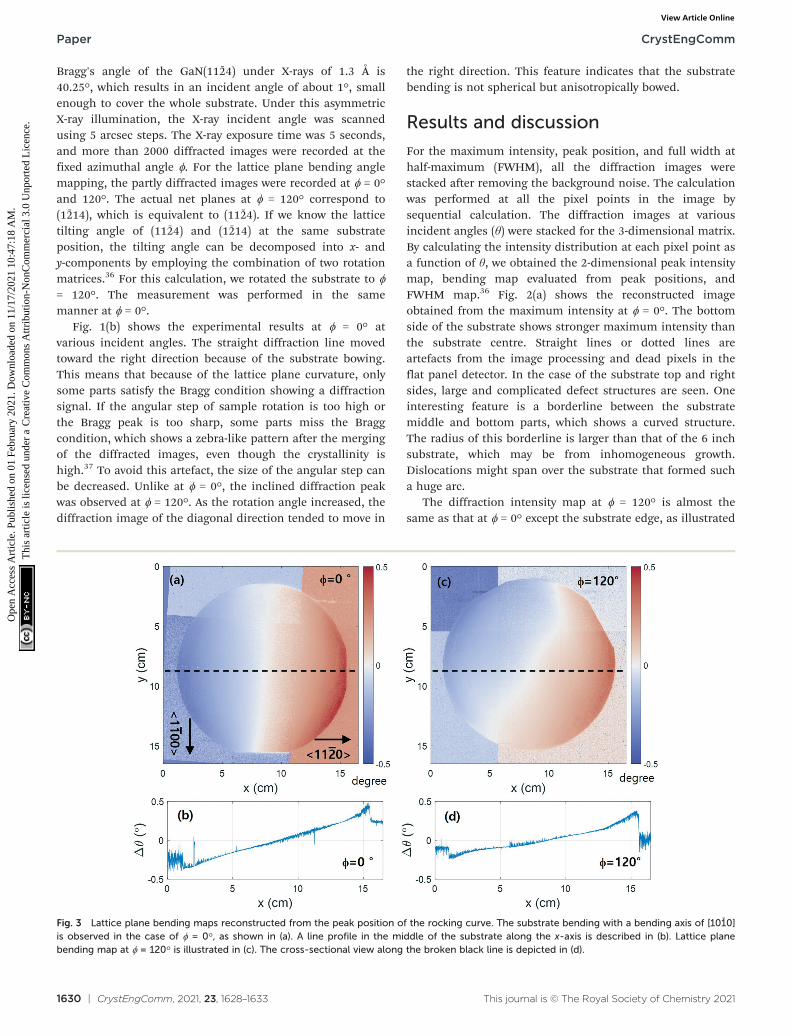
Fig. 3 Lattice plane bending maps reconstructed from the peak position of the rocking curve. The substrate bending with a bending axis of [101̄0]is observed in the case of ϕ = 0°, as shown in (a). A line profile in the middle of the substrate along the x-axis is described in (b). Lattice planebending map at ϕ = 120° is illustrated in (c). The cross-sectional view along the broken black line is depicted in (d).
CrystEngCommPaper
Ope
n A
cces
s A
rtic
le. P
ublis
hed
on 0
1 Fe
brua
ry 2
021.
Dow
nloa
ded
on 1
1/17
/202
1 10
:47:
18 A
M.
Thi
s ar
ticle
is li
cens
ed u
nder
a C
reat
ive
Com
mon
s A
ttrib
utio
n-N
onC
omm
erci
al 3
.0 U
npor
ted
Lic
ence
.View Article Online
CrystEngComm, 2021, 23, 1628–1633 | 1631This journal is © The Royal Society of Chemistry 2021
in Fig. 2(b). This is because, at the substrate edge, theincident angle is almost normal to the m-plane and theX-rays illuminate the substrate notch. Therefore, the X-rayilluminated crystal volume is larger than other regions thatshow stronger X-ray diffraction intensity. However, in otherpositions, the incident angle is small with respect to theGaN(0001) net planes making diffraction intensity weak andsensitive to the surface. For these reasons, the diffractionintensity at the sample edge is higher than that in otherplaces at a small incident angle.
To understand the lattice plane bending, we evaluated therocking curve of all the pixel points. The rocking curve peakposition map at ϕ = 0° is described in Fig. 3(a). The left sideof the substrate has a lower value, and the peak positiongradually increases as the position moves in the +x-direction,and the range of Δθ reached ∼0.8°. The derived radius ofcurvature from the cross-section along the broken black linewas 11 m, as shown in Fig. 3(b). An abrupt increase of the Δθ
was observed in the vicinity of the right-side edge (x ∼ 15cm). It is known that the dislocation density near the seedcrystal is high because of substrate bending.25 From thispoint of view, at x ∼ 15 cm, the dislocation density can behigher than that in other regions. The same analysis wasdone at ϕ = 120°, as shown in Fig. 3(c). The substrate bendingwas smaller than that at ϕ = 0°, which indicates anisotropicsubstrate bending, as shown in Fig. 1(c). The cross-section ofthe broken black line in Fig. 3(c) is depicted in Fig. 3(d). TheΔθ was ∼0.6°, and the radius of curvature calculated over therelatively flat area from x = 2 to 13 cm was 34 m, muchlonger than that at ϕ = 0°. The drastic change of Δθ wasobserved at x ∼ 3 cm and 13 cm, which implies abruptsubstrate bowing followed by the existence of highdislocation areas.
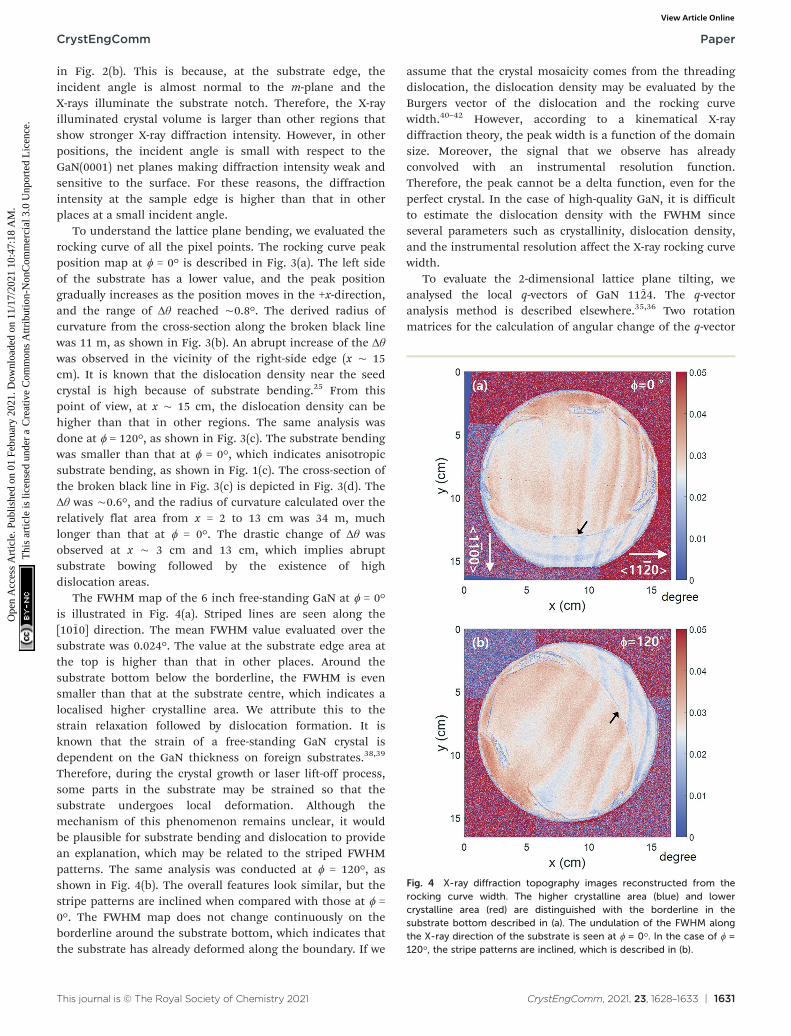
The FWHM map of the 6 inch free-standing GaN at ϕ = 0°is illustrated in Fig. 4(a). Striped lines are seen along the[101̄0] direction. The mean FWHM value evaluated over thesubstrate was 0.024°. The value at the substrate edge area atthe top is higher than that in other places. Around thesubstrate bottom below the borderline, the FWHM is evensmaller than that at the substrate centre, which indicates alocalised higher crystalline area. We attribute this to thestrain relaxation followed by dislocation formation. It isknown that the strain of a free-standing GaN crystal isdependent on the GaN thickness on foreign substrates.38,39
Therefore, during the crystal growth or laser lift-off process,some parts in the substrate may be strained so that thesubstrate undergoes local deformation. Although themechanism of this phenomenon remains unclear, it wouldbe plausible for substrate bending and dislocation to providean explanation, which may be related to the striped FWHMpatterns. The same analysis was conducted at ϕ = 120°, asshown in Fig. 4(b). The overall features look similar, but thestripe patterns are inclined when compared with those at ϕ =0°. The FWHM map does not change continuously on theborderline around the substrate bottom, which indicates thatthe substrate has already deformed along the boundary. If we
assume that the crystal mosaicity comes from the threadingdislocation, the dislocation density may be evaluated by theBurgers vector of the dislocation and the rocking curvewidth.40–42 However, according to a kinematical X-raydiffraction theory, the peak width is a function of the domainsize. Moreover, the signal that we observe has alreadyconvolved with an instrumental resolution function.Therefore, the peak cannot be a delta function, even for theperfect crystal. In the case of high-quality GaN, it is difficultto estimate the dislocation density with the FWHM sinceseveral parameters such as crystallinity, dislocation density,and the instrumental resolution affect the X-ray rocking curvewidth.
To evaluate the 2-dimensional lattice plane tilting, weanalysed the local q-vectors of GaN 112̄4. The q-vectoranalysis method is described elsewhere.35,36 Two rotationmatrices for the calculation of angular change of the q-vector
Fig. 4 X-ray diffraction topography images reconstructed from therocking curve width. The higher crystalline area (blue) and lowercrystalline area (red) are distinguished with the borderline in thesubstrate bottom described in (a). The undulation of the FWHM alongthe X-ray direction of the substrate is seen at ϕ = 0°. In the case of ϕ =120°, the stripe patterns are inclined, which is described in (b).
CrystEngComm Paper
Ope
n A
cces
s A
rtic
le. P
ublis
hed
on 0
1 Fe
brua
ry 2
021.
Dow
nloa
ded
on 1
1/17
/202
1 10
:47:
18 A
M.
Thi
s ar
ticle
is li
cens
ed u
nder
a C
reat
ive
Com
mon
s A
ttrib
utio
n-N
onC
omm
erci
al 3
.0 U
npor
ted
Lic
ence
.View Article Online

1632 | CrystEngComm, 2021, 23, 1628–1633 This journal is © The Royal Society of Chemistry 2021
were introduced. The projection of the q-vector to the (x, y)-plane is depicted in Fig. 5(a). In the vector plot, the arrowdirection indicates 2-dimensional inclination with respect tothe mean lattice plane bending angle. In particular, for theleft and the right sides, the lattice plane significantly headedto the substrate centre. Interestingly, the substrate bendingfrom top to bottom is much less than that in otherdirections. Fig. 5(b) shows the amplitude of the projectedvector in Fig. 5(a), which shows cylindrical bowing.
In the previous report on 4 inch free-standing GaN,35 themean FWHM over the substrate was about 0.009°, which isabout 3 times smaller than the current 6 inch substrate.However, the distribution of the FWHM map showedinhomogeneity originating from the nucleation sites, althoughthe mean FWHM is small. In this respect, we can understandthe inverse relationship between homogeneity and thedistribution of the FWHM. In highly inhomogeneous cases, thearea in the substrate can be separated into higher crystallineand lower crystalline regions, like the previous 4 inch case.35
However, for homogeneous cases, the mean FWHM of therocking curve is higher than that of the inhomogeneous case.The role of GaN seeds is to minimize the strain originating fromlattice mismatching during the ELO growth. In the case of aGaN crystal grown by seed-based methods, it shows a highdislocation density around the GaN seed but a low dislocationdensity away from the seed after the ELO growth. Therefore, the
crystallinity became inhomogeneous over the wafer, in whichthe substrate is composed of two different areas. In our 6 inchGaN crystal, the overall crystallinity was slightly lower than thatof other GaN crystals; however, the mean crystallinity washomogeneous.
Conclusions
6 inch free-standing GaN of high crystallinity was successfullygrown using the Na-flux LPE method. X-ray diffractiontopography, combined with a rocking curve imagingtechnique, showed huge boundaries between the high- andlow-crystalline areas. Bending analysis showed that the latticeplane is anisotropically bowed along the [101̄0] direction. Therocking curve width of GaN 112̄4 averaged over the substratewas 0.024 ± 0.003°, which indicates a high crystallinity andhomogeneous lattice plane over the substrate. We believethat there is a competition between substrate homogeneityand crystallinity.
Conflicts of interest
There are no conflicts of interest to declare.
Acknowledgements
The measurements were performed at SPring-8 (Proposal No.2020A1002, 2020A4503, 2020A4504, and 2020A1794) andSAGA-LS (Proposal No. 2001133S and 2007065S). This workwas partly supported by the MEXT “Research andDevelopment of Next-generation Semiconductor to RealizeEnergy-saving Society” (No. JPJ005357).
References
1 S. Nakamura, M. Senoh and T. Mukai, Jpn. J. Appl. Phys.,1993, 32, L8.
2 S. Nakamura, M. Senoh, N. Iwasa and S. Nagahama, Jpn. J.Appl. Phys., 1995, 34, L797.
3 N. Q. Zhang, S. Keller, G. Parish, S. Heikman, S. P.DenBaars and U. K. Mishra, IEEE Electron Device Lett.,2000, 21, 421.
4 W. Saito, Y. Takada, M. Kuraguchi, K. Tsuda, I. Omura, T.Ogura and H. Ohashi, IEEE Trans. Electron Devices, 2003, 50,2528.
5 T. Takeuchi, H. Amano, K. Hiramatsu, N. Sawaki and I.Akasaki, J. Cryst. Growth, 1991, 115, 634.
6 M. E. Lin, S. Strite, A. Agarwal, A. Salvador, G. L. Zhou, N.Teraguchi, A. Rockett and H. Morkoç, Appl. Phys. Lett.,1993, 62, 702.
7 Y. Kato, S. Kitamura, K. Hiramatsu and N. Sawaki, J. Cryst.Growth, 1994, 144, 133.
8 K. Hiramatsu, S. Itoh, H. Amano, I. Akasaki, N. Kuwano, T.Shiraishi and K. Oki, J. Cryst. Growth, 1991, 115, 628.
9 S. Tomiya, T. Hino, S. Goto, M. Takeya and M. Ikeda, IEEE J.Sel. Top. Quantum Electron., 2004, 10, 1277.
Fig. 5 Lattice plane bending direction projected to the (x, y)-plane isdescribed in (a). Symmetrical substrate bending with respect to they-direction is observed. The degree of substrate bending was visualisedfrom the magnitude of projected vectors (b).
CrystEngCommPaper
Ope
n A
cces
s A
rtic
le. P
ublis
hed
on 0
1 Fe
brua
ry 2
021.
Dow
nloa
ded
on 1
1/17
/202
1 10
:47:
18 A
M.
Thi
s ar
ticle
is li
cens
ed u
nder
a C
reat
ive
Com
mon
s A
ttrib
utio
n-N
onC
omm
erci
al 3
.0 U
npor
ted
Lic
ence
.View Article Online

CrystEngComm, 2021, 23, 1628–1633 | 1633This journal is © The Royal Society of Chemistry 2021
10 F. A. Marino, N. Faralli, T. Palacios, D. K. Ferry, S. M.Goodnick and M. Saraniti, IEEE Trans. Electron Devices,2010, 57, 353.
11 F. A. Ponce, B. S. Krusor, J. S. Major Jr., W. E. Plano andD. F. Welch, Appl. Phys. Lett., 1995, 67, 410.
12 H. Amano, N. Sawaki, I. Akasaki and Y. Toyoda, Appl. Phys.Lett., 1986, 48, 353.
13 H. Amano, I. Akasaki, K. Hiramatsu, N. Koide and N.Sawaki, Thin Solid Films, 1988, 163, 415.
14 I. Akasaki, H. Amano, Y. Koide, K. Hiramatsu and N. Sawaki,J. Cryst. Growth, 1989, 98, 209.
15 Y. Tian, Y. Shao, Y. Wu, X. Hao, L. Zhang, Y. Dai and Q.Huo, Sci. Rep., 2015, 5, 10748.
16 S. S. Park, I. Park and S. H. Choh, Jpn. J. Appl. Phys.,2000, 39, L1141.
17 M. K. Kelly, R. P. Vaudo, V. M. Phanse, L. Görgens, O.Ambacher and M. Stutzmann, Jpn. J. Appl. Phys., 1999, 38,L217.
18 C. R. Miskys, M. K. Kelly, O. Ambacher and M. Stutzmann,Phys. Status Solidi C, 2003, 0, 1627.
19 K. Motoki, T. Okahisa, N. Matsumoto, M. Matsushima, H.Kimura, H. Kasai, K. Takemoto, K. Uematsu, T. Hirano andM. Nakayama, Jpn. J. Appl. Phys., 2001, 40, L140.
20 B. Beaumont, Ph. Vennéguès and P. Gibart, Phys. StatusSolidi B, 2001, 227, 1.
21 C. Chu, F. Lai, J. Chu, C. Yu, C. Lin, H. Kuo and S. C. Wang,J. Appl. Phys., 2004, 95, 3916.
22 S. Porowski, MRS Internet J. Nitride Semicond. Res., 1999, 4,27.
23 K. Fujito, S. Kubo, H. Nagaoka, T. Mochizuki, H. Namita andS. Nagao, J. Cryst. Growth, 2009, 311, 3011.
24 H. Fujikura, T. Konno, T. Suzuki, T. Kitamura, T. Fujimotoand T. Yoshida, Jpn. J. Appl. Phys., 2018, 57, 065502.
25 T. Hashimoto, F. Wu, J. S. Speck and S. Nakamura, Nat.Mater., 2007, 6, 568.
26 Y. Song, W. Wang, W. Yuan, X. Wu and X. Chen, J. Cryst.Growth, 2003, 247, 275.
27 X. L. Chen, Sci. Technol. Adv. Mater., 2005, 6, 766.
28 F. Kawamura, H. Umeda, M. Morishita, M. Kawahara, M.Yoshimura, Y. Mori, T. Sasaki and Y. Kitaoka, Jpn. J. Appl.Phys., 2006, 45, L1136.
29 Y. Mori, Y. Kitaoka, M. Imade, N. Miyoshi, M. Yoshimuraand T. Sasaki, Phys. Status Solidi A, 2010, 207, 1283.
30 Y. Mori, Y. Kitaoka, M. Imade, N. Miyoshi, M. Yoshimuraand T. Sasaki, Phys. Status Solidi C, 2011, 8, 1445.
31 Y. Mori, M. Imade, M. Maruyama and M. Yoshimura, ECS J.Solid State Sci. Technol., 2013, 2, N3068.
32 M. Imade, M. Imanishi, Y. Todoroki, H. Imabayashi, D.Matsuo, K. Murakami, H. Takazawa, A. Kitamoto, M.Maruyama, M. Yoshimura and Y. Mori, Appl. Phys. Express,2014, 7, 035503.
33 Y. Mori, M. Imanishi, K. Murakami and M. Yoshimura, Jpn.J. Appl. Phys., 2019, 58, SC0803.
34 Y. Mori, M. Imade, K. Murakami, H. Takazawa, H.Imabayashi, Y. Todoroki, K. Kitamoto, M. Maruyama, M.Yoshimura, Y. Kitaoka and T. Sasaki, J. Cryst. Growth,2020, 350, 72.
35 J. Kim, O. Seo, C. Song, Y. Chen, S. Hiroi, Y. Irokawa, T.Nabatame, Y. Koidea and O. Sakata, CrystEngComm,2018, 20, 7761.
36 J. Kim, O. Seo, C. Song, S. Hiroi, Y. Chen, Y. Irokawa, T.Nabatame, Y. Koide and O. Sakata, Appl. Phys. Express,2018, 11, 081002.
37 O. Seo, J. M. Kim, C. Song, Y. Lou, L. S. R. Kumara, S. Hiroi,Y. Chen, Y. Katsuya, Y. Irokawa, T. Nabatame, Y. Koide andO. Sakata, AIP Adv., 2018, 8, 075318.
38 K. Yamane, T. Matsubara, T. Yamamoto, N. Okada, A.Wakahara and K. Tadatomo, J. Appl. Phys., 2016, 119, 045707.
39 F. Lipski, M. Klein, X. Yao and F. Scholz, J. Cryst. Growth,2012, 352, 235.
40 C. G. Dunn and E. F. Kogh, Acta Metall., 1957, 5, 548.41 T. Metzger, R. Höpler, E. Born, O. Ambacher, M. Stutzmann,
R. Stömmer, M. Schuster, H. Göbel, S. Christiansen, M.Albrecht and H. P. Strunk, Philos. Mag. A, 1998, 77, 1013.
42 R. Chierchia, T. Böttcher, H. Heinke, S. Einfeldt, S. Figgeand D. Hommel, J. Appl. Phys., 2003, 93, 8918.
CrystEngComm Paper
Ope
n A
cces
s A
rtic
le. P
ublis
hed
on 0
1 Fe
brua
ry 2
021.
Dow
nloa
ded
on 1
1/17
/202
1 10
:47:
18 A
M.
Thi
s ar
ticle
is li
cens
ed u
nder
a C
reat
ive
Com
mon
s A
ttrib
utio
n-N
onC
omm
erci
al 3
.0 U
npor
ted
Lic
ence
.View Article Online


![Electron microscopy of gallium nitride growth on ...€¦ · crystal diamond [4, 5], whilst also being more affordable. Growth of GaN on crystalline diamond and poly-crystalline diamond](https://static.fdocuments.us/doc/165x107/601926019f77915fc30e994a/electron-microscopy-of-gallium-nitride-growth-on-crystal-diamond-4-5-whilst.jpg)