High Throughput Maskless Lithography - MAPPER...blanker 110 x 10 MHz 13,000 x 49 x 70 MHz Ge...
19
High Throughput Maskless Lithography Sokudo lithography breakfast forum July 14 th 2010 Bert Jan Kampherbeek, VP Market Development and co-founder
Transcript of High Throughput Maskless Lithography - MAPPER...blanker 110 x 10 MHz 13,000 x 49 x 70 MHz Ge...

High Throughput Maskless Lithography
Sokudo lithography breakfast forum
July 14th 2010
Bert Jan Kampherbeek, VP Market Development and co-founder

2Sokudo lithography breakfast forum July 14th 2010
Agenda
• MAPPER’s Objective
• MAPPER’s Status
• MAPPER’s Roadmap

3Sokudo lithography breakfast forum July 14th 2010
MAPPER’s objective: Provide lithography solution for 32 nm hp and beyond
• Provide 10 wph lithography unit in ~ 1 m2 per unit at a competitive price
• Cluster several 10 wph units together, for example 10 units for 100 wph
• Application of first generation MAPPER manufacturing machines: Contact and via layers, 32 nm hp (22nm logic node) Metal layers, 32 nm hp Cutting / filling layers in double patterning, 16 nm hp (11nm logic node)
• MAPPER solution is extendable to at least:
16 nm hp random patterning @ 10 wph in 1 m2
8 nm hp with pitch division and cut/fill @ 10 wph in 1 m2
MAPPER Objective

4Sokudo lithography breakfast forum July 14th 2010
MAPPER builds a system with 13,000 parallel electron beams for 10 wph
MAPPER Objective
Key numbers 22nm node:HVM pre-alpha
#beams and data channels 13,000 110
Spotsize: 25 nm 35 nm
Beam current: 13 nA 0.3 nA
Datarate/channel 3.5 Gbs 20 MHz
Acceleration voltage 5 kV 5 kV
Nominal dose 30 µC/cm2 30 µC/cm2
Throughput @ nominal dose 10 wph 0.002 wph
Pixel size @ nominal dose 3.5nm 2.25 nm
Wafer movement Scanning Static

5Sokudo lithography breakfast forum July 14th 2010
Tool cluster for 100 wph
MAPPER single column tool. Upgrade to 13,000 beam for 10WPH
Interface to track
MAPPER Objective
6Sokudo lithography breakfast forum July 14th 2010
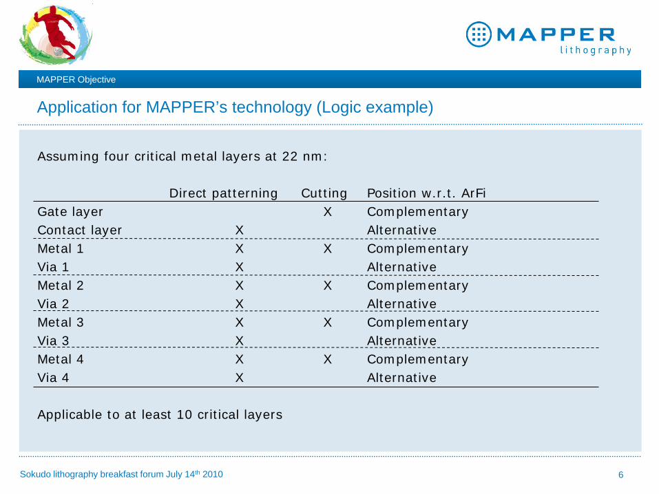
Application for MAPPER’s technology (Logic example)
Assuming four critical metal layers at 22 nm:
Direct patterning Cutting Position w.r.t. ArFiGate layer X ComplementaryContact layer X AlternativeMetal 1 X X ComplementaryVia 1 X AlternativeMetal 2 X X ComplementaryVia 2 X AlternativeMetal 3 X X ComplementaryVia 3 X AlternativeMetal 4 X X ComplementaryVia 4 X Alternative
Applicable to at least 10 critical layers
MAPPER Objective
7Sokudo lithography breakfast forum July 14th 2010
Agenda
• MAPPER’s Objective
• MAPPER’s Status
• MAPPER’s Roadmap

8Sokudo lithography breakfast forum July 14th 2010
Overview current MAPPER machine
• 1.3 x 1.3 m footprint containing 300 mm wafer stage
• Electron optics is completely in vacuum Source used for CRT application Lens arrays manufactured with MEMS
techniques
• Wafer stage is in vacuum Long stroke motors outside shielding Short stroke magnetically shielded
• Data path is in the sub-fab (not in picture) Blanker chip with integrated photodiodes
switches electron beams Data path connected through fibers with
electron optics
MAPPER Status
9Sokudo lithography breakfast forum July 14th 2010
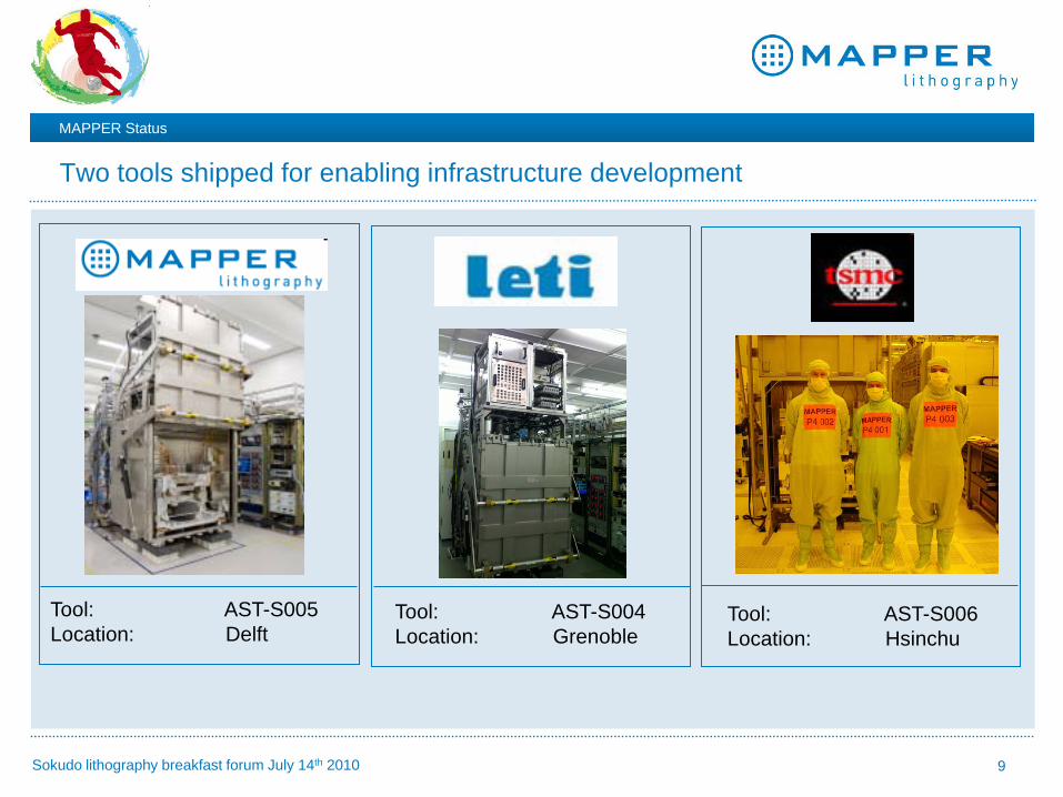
Two tools shipped for enabling infrastructure development
Tool: AST-S005Location: Delft
Tool: AST-S006Location: Hsinchu
Tool: AST-S004Location: Grenoble
MAPPER Status

10Sokudo lithography breakfast forum July 14th 2010
Results of MAPPER prototype tool @ TSMC (1/2)
MAPPER Status

11Sokudo lithography breakfast forum July 14th 2010
Results of MAPPER prototype tool @ TSMC (2/2)
MAPPER Status

12Sokudo lithography breakfast forum July 14th 2010
Results of MAPPER prototype tool @ CEA-Leti (1/4)
MAPPER Status

13Sokudo lithography breakfast forum July 14th 2010
Coat/Develop Track supporting
Results of MAPPER prototype tool @ CEA-Leti (2/4)
MAPPER Status

14Sokudo lithography breakfast forum July 14th 2010
Results of MAPPER prototype tool @ CEA-Leti (3/4)
MAPPER Status
15Sokudo lithography breakfast forum July 14th 2010
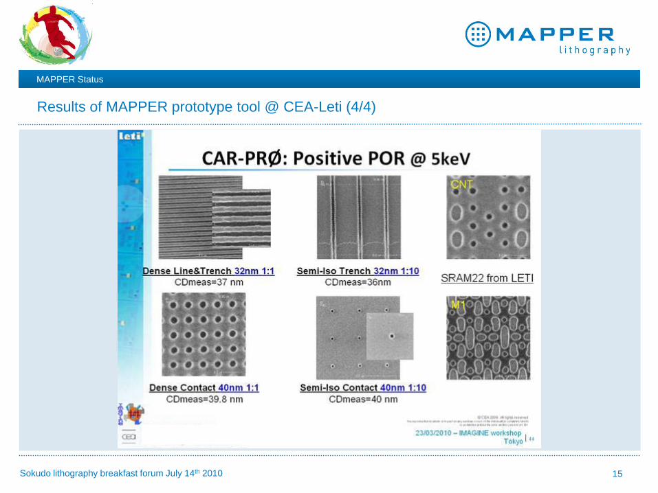
Results of MAPPER prototype tool @ CEA-Leti (4/4)
MAPPER Status

16Sokudo lithography breakfast forum July 14th 2010
Agenda
• MAPPER’s Objective
• MAPPER’s Status
• MAPPER’s Roadmap
17Sokudo lithography breakfast forum July 14th 2010
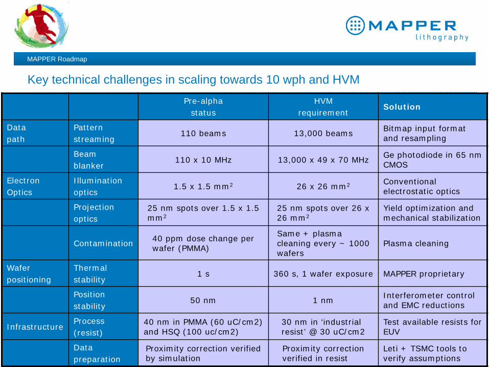
Key technical challenges in scaling towards 10 wph and HVMPre-alpha
statusHVM
requirementSolution
Datapath
Patternstreaming
110 beams 13,000 beams Bitmap input format and resampling
Beamblanker
110 x 10 MHz 13,000 x 49 x 70 MHz Ge photodiode in 65 nm CMOS
ElectronOptics
Illuminationoptics
1.5 x 1.5 mm2 26 x 26 mm2 Conventional electrostatic optics
Projectionoptics
25 nm spots over 1.5 x 1.5 mm2
25 nm spots over 26 x 26 mm2
Yield optimization and mechanical stabilization
Contamination 40 ppm dose change per wafer (PMMA)
Same + plasma cleaning every ~ 1000 wafers
Plasma cleaning
Waferpositioning
Thermalstability
1 s 360 s, 1 wafer exposure MAPPER proprietary
Positionstability
50 nm 1 nm Interferometer control and EMC reductions
InfrastructureProcess(resist)
40 nm in PMMA (60 uC/cm2) and HSQ (100 uc/cm2)
30 nm in ‘industrial resist’ @ 30 uC/cm2
Test available resists for EUV
Datapreparation
Proximity correction verified by simulation
Proximity correction verified in resist
Leti + TSMC tools to verify assumptions
MAPPER Roadmap

19Sokudo lithography breakfast forum July 14th 2010
Conclusions
• MAPPER’s technology provides a 10 wph system on a 1 m2 footprint at low cost
• MAPPER’s technology is an alternative for both direct patterning and pitch splitting with cutting and filling, this makes the technology viable for > 10 critical layers / chip
• MAPPER has installed two machines in the field, one at TSMC and one at CEA – Leti
• Both machines, designed for 45 nm hp resolution, resolve ~ 30 nm hp in CAR
• At CEA-Leti a tool assessment and infrastructure program is ongoing: IMAGINE
• Solutions for scaling to 10 wph are available and are scalable for at least 3 generations
• In our opinion there are no fundamental roadblocks left

20Sokudo lithography breakfast forum July 14th 2010
Thank you


![BICONICAL ANTENNAS BICOLOG · Dimensions [L x W x D] 350 x 160 x 140 mm Nominal Impedance 50 Ohm Weight 350 g Calibration Points 104 (5 MHz and 10 MHz steps) Design Biconical RF Connection](https://static.fdocuments.us/doc/165x107/6092cb9f15c44936d1005998/biconical-antennas-bicolog-dimensions-l-x-w-x-d-350-x-160-x-140-mm-nominal-impedance.jpg)
