High-speed parallel Viterbi decoding: algorithm and VLSI...
10
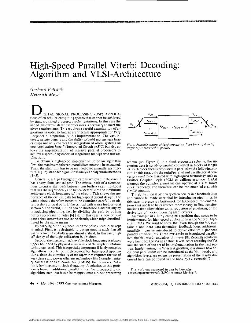
High-speed Parallel Viterbi Decoding: Algorithm and VLSI-Architecture Gerhard Fettweis Heinrich Meyr U IGITAL SIGNAL PROCESSING (DSP) APPLICA- tions often require computing speeds that cannot be achieved by standard signal processor implementations. In this case the use of customized dataflow processors is necessary to meet the given requirements. This requires a careful examination of al- gorithms in order to find an architecture appropriate for Very Large-scale Integration (VLSI) implementation. The vast in- crease in gate density and the ability to build increasingly larg- er chips not only enables the integration of whole systems on one Application Specific Integrated Circuit (ASIC) but also al- lows the implementation of massive parallel processors to achieve a speedup by orders of magnitude for high data rate ap- plications. To obtain a high-speed implementation of an algorithm first, the maximum inherent parallelism needs to be extracted. Then, the algorithm has to be mapped onto a parallel architec- ture, e.g., by standard signal-flow analysis or algebraic methods Generally, a high throughput-rate is achieved if the circuit has a very short critical path. The critical path of a synchro- nous circuit is that path between two buffers (e.g., flip-flops) that has the largest delay and hence, determines the maximum achievable clock frequency of the circuit. This shows the im- portance of the critical path for high-speed circuit design. The whole circuit therefore needs to be examined carefully to ob- tain a short critical path. If the critical path is in a feedforward section of the circuit, it often can be shortened substantially by introducing pipelining, i.e., by dividing the path by adding buffers according to rules [6] [7]. In this case, a new critical path arises somewhere else in the circuit, which might be elimi- nated by the same means. By carrying out this procedure three points need to be kept in mind. First, it is desirable to design circuits such that all paths between two buffers are almost critical. In this case, high efficiency of the logic utilization is obtained. Second, the maximum achievable clock frequency is always upper bounded by physical constraints of the implementation technology used. This is especially important if fairly complex algorithms need to be implemented for high-speed applica- tions, since the complexity of the algorithm requires the use of very dense and power efficient technology like Complementa- ry Metal Oxide Semiconductor (CMOS), that however, has a fairly low maximum clock frequency. A solution to this prob- lem is found if additional parallelism can be introduced to the algorithm such that it can be mapped onto a block processing [ 1-51. 'nM+M- 1 l - Fig. 1. Principle scheme of block processing. Each block of data (of length M) is processed in parallel. scheme (see Figure 1). In a block processing scheme, the in- coming data is serial-to-parallel converted in blocks of length M. Each block then is processed in parallel by the following cir- cuit. In this case, only the serial/parallel and parallel/serial con- verters need to be realized with high-speed technology such as Emitter Coupled Logic (ECL) or gallium arsenide (GaAs) whereas the complex algorithm can operate at a 1/M lower clock frequency, and therefore, can be implemented e.g., with CMOS circuits. Third, the critical path very often occurs in a feedback loop and cannot be made uncritical by introducing pipelining. In this case, it presents a bottleneck for high-speed implementa- tions that needs to be examined more closely to find transfor- mations that allow either an introduction of pipelining or the derivation of block-processing architectures. An example of a fairly complex algorithm that needs to be implemented for high-speed applications is the Viterbi Algo- rithm (VA). We want to show that even though the VA con- tains a nonlinear data-dependent feedback loop, additional parallelism can be introduced to derive efficient high-speed parallel architectures. Three levels exist to introduced parallel- ism, the bit-, word-, and algorithm-level [8]. Recently solutions were found for the VA at all three levels. After recalling the VA and the state of the art of its implementation in the next sec- tion, Implementing the Viterbi Algorithm, it is shown how ad- ditional parallelism can be introduced at the bit-, word-, and algorithm-levels. An extensive presentation of the results dis- cussed here can be found in the book by G. Fettweis [9]. This work was supported in part by Deutsche Forschungsgemeinschaft (DFG), contract Me 65 1/7. 46 May 199 1 - IEEE Communications Magazine 01 63-6804/9 1 /0005-0046 $01 .OO 199 1 IEEE Authorized licensed use limited to: The University of Toronto. Downloaded on July 13, 2009 at 16:27 from IEEE Xplore. Restrictions apply.
Transcript of High-speed parallel Viterbi decoding: algorithm and VLSI...
High-speed Parallel Viterbi Decoding: Algorithm and VLSI-Architecture Gerhard Fettweis Heinrich Meyr
U IGITAL SIGNAL PROCESSING (DSP) APPLICA- tions often require computing speeds that cannot be achieved by standard signal processor implementations. In this case the use of customized dataflow processors is necessary to meet the given requirements. This requires a careful examination of al- gorithms in order to find an architecture appropriate for Very Large-scale Integration (VLSI) implementation. The vast in- crease in gate density and the ability to build increasingly larg- er chips not only enables the integration of whole systems on one Application Specific Integrated Circuit (ASIC) but also al- lows the implementation of massive parallel processors to achieve a speedup by orders of magnitude for high data rate ap- plications.
To obtain a high-speed implementation of an algorithm first, the maximum inherent parallelism needs to be extracted. Then, the algorithm has to be mapped onto a parallel architec- ture, e.g., by standard signal-flow analysis or algebraic methods
Generally, a high throughput-rate is achieved if the circuit has a very short critical path. The critical path of a synchro- nous circuit is that path between two buffers (e.g., flip-flops) that has the largest delay and hence, determines the maximum achievable clock frequency of the circuit. This shows the im- portance of the critical path for high-speed circuit design. The whole circuit therefore needs to be examined carefully to ob- tain a short critical path. If the critical path is in a feedforward section of the circuit, it often can be shortened substantially by introducing pipelining, i.e., by dividing the path by adding buffers according to rules [6] [7]. In this case, a new critical path arises somewhere else in the circuit, which might be elimi- nated by the same means.
By carrying out this procedure three points need to be kept in mind. First, it is desirable to design circuits such that all paths between two buffers are almost critical. In this case, high efficiency of the logic utilization is obtained.
Second, the maximum achievable clock frequency is always upper bounded by physical constraints of the implementation technology used. This is especially important if fairly complex algorithms need to be implemented for high-speed applica- tions, since the complexity of the algorithm requires the use of very dense and power efficient technology like Complementa- ry Metal Oxide Semiconductor (CMOS), that however, has a fairly low maximum clock frequency. A solution to this prob- lem is found if additional parallelism can be introduced to the algorithm such that it can be mapped onto a block processing
[ 1-51.
'nM+M- 1 l- Fig. 1. Principle scheme of block processing. Each block of data (of length M) is processed in parallel.
scheme (see Figure 1). In a block processing scheme, the in- coming data is serial-to-parallel converted in blocks of length M. Each block then is processed in parallel by the following cir- cuit. In this case, only the serial/parallel and parallel/serial con- verters need to be realized with high-speed technology such as Emitter Coupled Logic (ECL) or gallium arsenide (GaAs) whereas the complex algorithm can operate at a 1/M lower clock frequency, and therefore, can be implemented e.g., with CMOS circuits.
Third, the critical path very often occurs in a feedback loop and cannot be made uncritical by introducing pipelining. In this case, it presents a bottleneck for high-speed implementa- tions that needs to be examined more closely to find transfor- mations that allow either an introduction of pipelining or the derivation of block-processing architectures.
An example of a fairly complex algorithm that needs to be implemented for high-speed applications is the Viterbi Algo- rithm (VA). We want to show that even though the VA con- tains a nonlinear data-dependent feedback loop, additional parallelism can be introduced to derive efficient high-speed parallel architectures. Three levels exist to introduced parallel- ism, the bit-, word-, and algorithm-level [ 8 ] . Recently solutions were found for the VA at all three levels. After recalling the VA and the state of the art of its implementation in the next sec- tion, Implementing the Viterbi Algorithm, it is shown how ad- ditional parallelism can be introduced at the bit-, word-, and algorithm-levels. An extensive presentation of the results dis- cussed here can be found in the book by G. Fettweis [9 ] .
This work was supported in part by Deutsche Forschungsgemeinschaft (DFG), contract Me 65 1/7.
46 May 199 1 - IEEE Communications Magazine 01 63-6804/9 1 /0005-0046 $01 .OO 199 1 IEEE
Authorized licensed use limited to: The University of Toronto. Downloaded on July 13, 2009 at 16:27 from IEEE Xplore. Restrictions apply.
I Latch
, # I
k k i l
a. A trellis with N = 2 states
Y1.k + ‘11,k A
k-D \ D: Survivor Depth
._... W
r2.k k k + l Time
b. Decoding the optimum path to node s ~ , ~ + ~ at time k+ 1 and
paths showing that they merge when traced back D steps
Fig. 2. Examples of trellis and optirrum paths.
Implementing the Viterbi Algorithm Dynamic programming is a well-established approach for a
large variety of problems concerning multistage decision pro- cesses [ lo]. One specific application of dynamic programming is the search for the best path through a graph of weighted branches. These branch weights will hereafter be referred to as branch metrics. The path through the graph to be found, is the one with the maximum (or minimum) cost, i.e., the maximum value of accumulated branch metrics. An example of such a graph is the trellis (the state transition diagram) of a discrete- time finite state machine. The state sequence of the finite state machine marks a path through the trellis. If this path is to be es- timated with the help of noisy measurements of the output of the finite state machine, and if this is solved by dynamic pro- gramming, then in communications this is called the VA [ 1 1 ]. The VA was introduced in 1967 as a method to decode convolutional codes [12]. In the meantime the VA has found widespread applications in communications as e.g., in digital transmission, magnetic recording, and speech recognition. A comprehensive tutorial on the VA is given [ 131. A brief intro- duction to the VA will be discussed.
The Viterbi Algorithm Given: a discrete-time finite state machine with N states.
Without loss of generality we assume that the transition dia- gram and the transition rate l /Tare constant in time. The trel- lis, which shows the transition dynamics, is a two-dimensional graph that is described in vertical direction by N states si and in horizontal direction by time instances kT(T= 1). The states of time instance, k, are connected with those of time k+ 1 by the branches of time interval (k,k+ 1). Below we refer to a specific state si at time instance k as node si The branch between two nodes corresponds to a possible state transition. A simple ex- ample of a trellis is given in Figure 2a for N = 2 states. The nota- tion used can be summarized as follows:
9 N - number of states k - time instance
9 si - i-th possible state, is { l , ..., Si,k - node: i-th possible state of time instance k Now, the finite state machine chooses a path through the
trellis and with the help ofthe observed state transitions (over a noisy channel) the branch metrics of time interval (k,k+ 1) are computed.
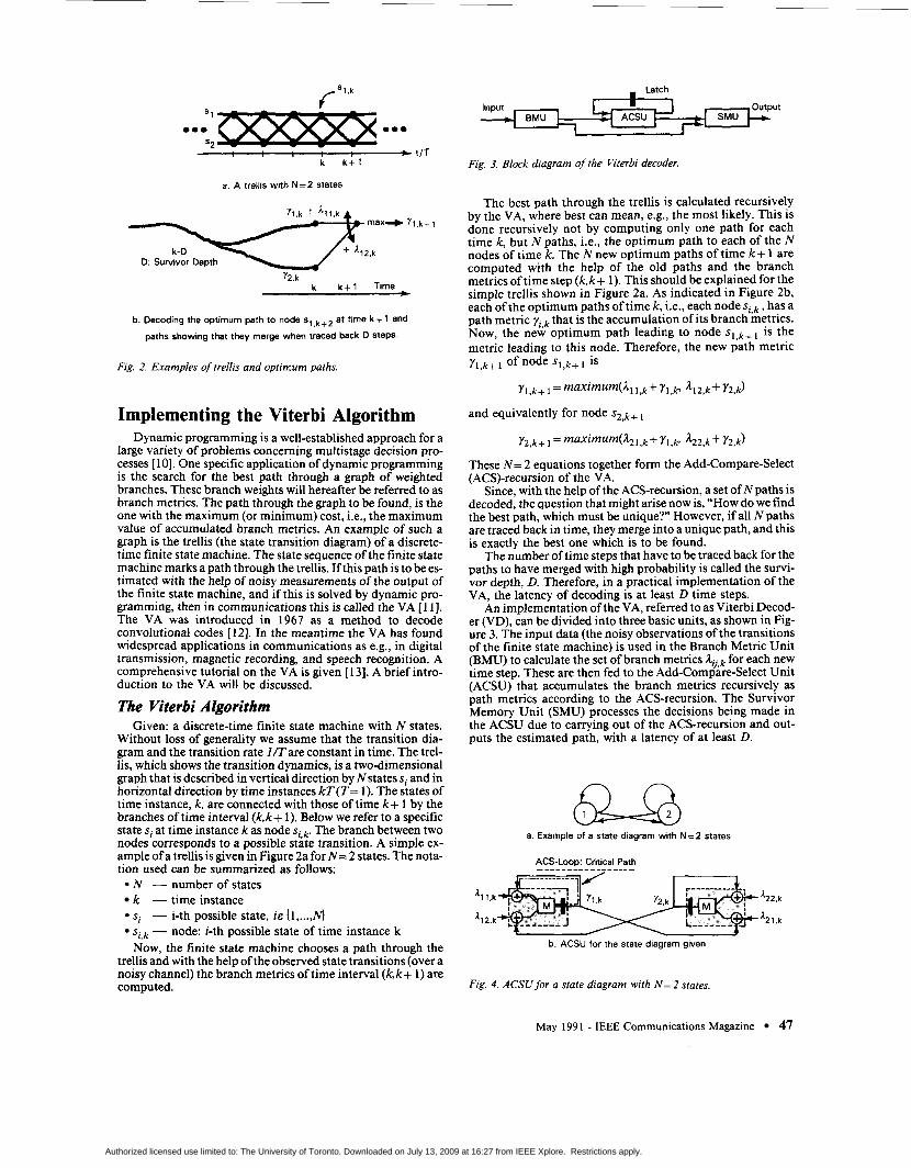
Fig. 3. Block diagram of the Viterbi decoder
The best path through the trellis is calculated recursively by the VA, where best can mean, e.g., the most likely. This is done recursively not by computing only one path for each time k, but N paths, i.e., the optimum path to each of the N nodes of time k. The N new optimum paths of time k+ 1 are computed with the help of the old paths and the branch metrics of time step (k,k+ 1). This should be explained for the simple trellis shown in Figure 2a. As indicated in Figure 2b, each of the optimum paths of time k, i.e., each node S , , k , has a path metric Yi,k that is the accumulation of its branch metrics. Now, the new optimum path leading to node S l , k + l is the metric leading to this node. Therefore, the new path metric Y l , k + 1 Of node S l , k + 1 is
Yl ,k+ 1 I , k + Y l , b 4 2 , k + y2,k)
and equivalently for node SZ,k+,
Y2,k+ I =maximum(&l,k+ Y l , k &2,k+y2,k)
These N = 2 equations together form the Add-Compare-Select (ACS)-recursion of the VA.
Since, with the help of the ACS-recursion, a set of N paths is decoded, the question that might arise now is, “How do we find the best path, which must be unique?” However, if all N paths are traced back in time, they merge into a unique path, and this is exactly the best one which is to be found.
The number of time steps that have to be traced back for the paths to have merged with high probability is called the survi- vor depth, D. Therefore, in a practical implementation of the VA, the latency of decoding is at least D time steps.
An implementation of the VA, referred to as Viterbi Decod- er (VD), can be divided into three basic units, as shown in Fig- ure 3. The input data (the noisy observations of the transitions of the finite state machine) is used in the Branch Metric Unit (BMU) to calculate the set of branch metrics A0.k for each new time step. These are then fed to the Add-Compare-Select Unit (ACSU) that accumulates the branch metrics recursively as path metrics according to the ACS-recursion. The Survivor Memory Unit (SMU) processes the decisions being made in the ACSU due to carrying out of the ACS-recursion and out- puts the estimated path, with a latency of at least D.
a. Example of a state diagram with N=2 states
ACS-Loop, Critical Path - --------------- - ‘1 1.k ‘22.k
‘12.k 3 l . k
b. ACSU for the state diagram given
Fig. 4. ACSU for a state diagram with N = 2 states.
May 1991 - IEEE Communications Magazine 47
Authorized licensed use limited to: The University of Toronto. Downloaded on July 13, 2009 at 16:27 from IEEE Xplore. Restrictions apply.
4 I
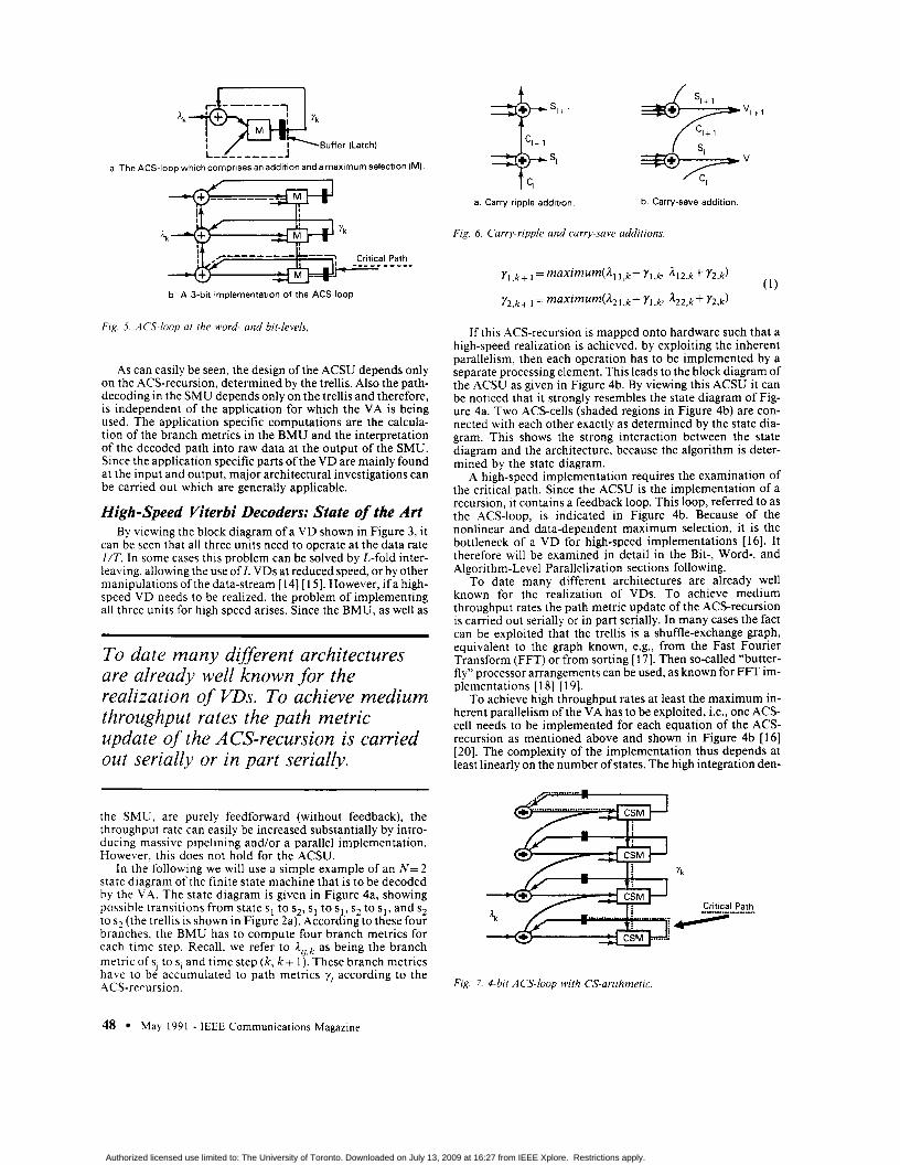
a. The ACS-loop which comprises an addition and a maximum selection (MI.
yk
Critical Path 1 - _--_----_
b. A 3-bit implementation of the ACS-loop.
Fig. 5. ACS-loop at the word- and bit-levels,
As can easily be seen, the design of the ACSU depends only on the ACS-recursion, determined by the trellis. Also the path- decoding in the SMU depends only on the trellis and therefore, is independent of the application for which the VA is being used. The application specific computations are the calcula- tion of the branch metrics in the BMU and the interpretation of the decoded path into raw data at the output of the SMU. Since the application specific parts of the VD are mainly found at the input and output, major architectural investigations can be camed out which are generally applicable.
High-speed Viterbi Decoders: State of the Art By viewing the block diagram of a VD shown in Figure 3, it
can be seen that all three units need to operate at the data rate 1/T. In some cases this problem can be solved by L-fold inter- leaving, allowing the use of L VDs at reduced speed, or by other manipulations of the data-stream [ 141 [ 151. However, if a high- speed VD needs to be realized, the problem of implementing all three units for high speed arises. Since the BMU, as well as
To date many different architectures are already well known for the realization of VDs. To achieve medium throughput rates the path metric update of the ACS-recursion is carried out serially or in part serially.
the SMU, are purely feedforward (without feedback), the throughput rate can easily be increased substantially by intro- ducing massive pipelining and/or a parallel implementation. However, this does not hold for the ACSU.
In the following we will use a simple example of an N = 2 state diagram of the finite state machine that is to be decoded by the VA. The state diagram is given in Figure 4a, showing possible transitions from state s1 to s2 , s , to sl,, s2 to sl, and s2 to s2 (the trellis is shown in Figure 2a). According to these four branches, the BMU has to compute four branch metrics for each time step. Recall, we refer to A,,,k as being the branch metric of s, to s, and time step ( k , k+ 1). These branch metrics have to be accumulated to path metrics y, according to the ACS-rerursion.
SI VI <
a. Carry-ripple addition, b. Carry-save addition
Fig. 6. Carry-ripple and carry-save additions.
If this ACS-recursion is mapped onto hardware such that a high-speed realization is achieved, by exploiting the inherent parallelism, then each operation has to be implemented by a separate processing element. This leads to the block diagram of the ACSU as given in Figure 4b. By viewing this ACSU it can be noticed that it strongly resembles the state diagram of Fig- ure 4a. Two ACS-cells (shaded regions in Figure 4b) are con- nected with each other exactly as determined by the state dia- gram. This shows the strong interaction between the state diagram and the architecture, because the algorithm is deter- mined by the state diagram.
A high-speed implementation requires the examination of the critical path. Since the ACSU is the implementation of a recursion, it contains a feedback loop. This loop, referred to as the ACS-loop, is indicated in Figure 4b. Because of the nonlinear and data-dependent maximum selection, it is the bottleneck of a VD for high-speed implementations [ 161. It therefore will be examined in detail in the Bit-, Word-. and Algorithm-Level Parallelization sections following.
To date many different architectures are already well known for the realization of VDs. To achieve medium throughput rates the path metric update of the ACS-recursion is carried out serially or in part serially. In many cases the fact can be exploited that the trellis is a shuffle-exchange graph, equivalent to the graph known, e.g., from the Fast Fourier Transform (FFT) or from sorting [ 171. Then so-called “butter- fly” processor arrangements can be used, as known for FFT im- plementations [ 181 [ 191.
To achieve high throughput rates at least the maximum in- herent parallelism of the VA has to be exploited, i.e., one ACS- cell needs to be implemented for each equation of the ACS- recursion as mentioned above and shown in Figure 4b [16] [20]. The complexity of the implementation thus depends at least linearly on the number of states. The high integration den-
...- +&+ . ........ ..
Critical Path
Fig. 7. 4-bit ACS-loop with CS-arithmetic.
48 May 1991 - IEEE Communications Magazine
Authorized licensed use limited to: The University of Toronto. Downloaded on July 13, 2009 at 16:27 from IEEE Xplore. Restrictions apply.
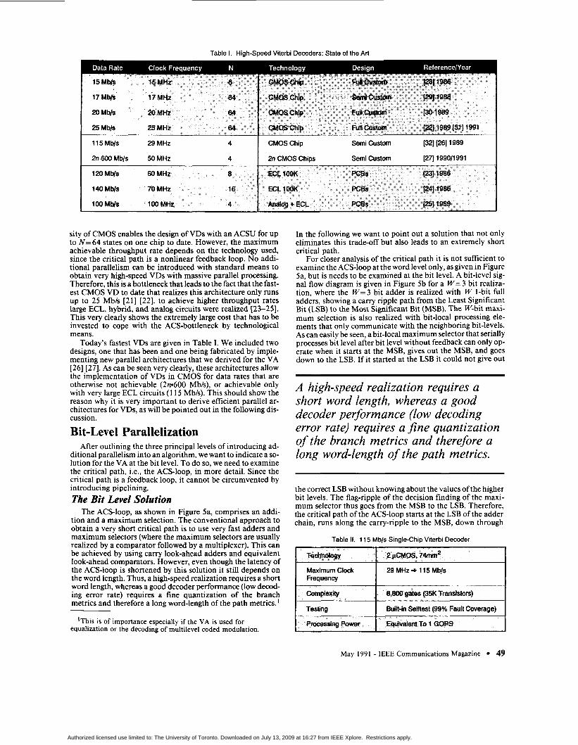
Table 1. High-speed Viterbi Decoders: State of the Art
CMOS Chip Semi Custom [32] [26] 1989 I 2n CMOS Chips Semi Custom [27] 1990/1991
11 5 Mb/s 29 MHz 4
2n.600 Mb/S 50 MHz 4
sity of CMOS enables the design of VDs with an ACSU for up to N = 64 states on one chip to date. However, the maximum achievable throughput rate depends on the technology used, since the critical path is a nonlinear feedback loop. No addi- tional parallelism can be introduced with standard means to obtain very high-speed VDs with massive parallel processing. Therefore, this is a bottleneck that leads to the fact that the fast- est CMOS VD to date that realizes this architecture only runs up to 25 Mb/s [21] [22]. to achieve higher throughput rates large ECL, hybrid, and analog circuits were realized [23-251. This very clearly shows the extremely large cost that has to be invested to cope with the ACS-bottleneck by technological means.
Today's fastest VDs are given in Table I. We included two designs, one that has been and one being fabricated by imple- menting new parallel architectures that we derived for the VA [26] [27]. As can be seen very clearly, these architectures allow the implementation of VDs in CMOS for data rates that are otherwise not achievable (2n*600 Mb/s), or achievable only with very large ECL circuits (1 15 Mb/s). This should show the reason why it is very important to derive efficient parallel ar- chitectures for VDs, as will be pointed out in the following dis- cussion.
Bit-Level Parallelization After outlining the three principal levels of introducing ad-
ditional parallelism into an algorithm, we want to indicate a so- lution for the VA at the bit level. To do so, we need to examine the critical path, i.e., the ACS-loop, in more detail. Since the critical path is a feedback loop, it cannot be circumvented by introducing pipelining. The Bit Level Solution
The ACS-loop, as shown in Figure 5a, comprises an addi- tion and a maximum selection. The conventional approach to obtain a very short critical path is to use very fast adders and maximum selectors (where the maximum selectors are usually realized by a comparator followed by a multiplexer). This can be achieved by using carry look-ahead adders and equivalent look-ahead comparators. However, even though the latency of the ACS-loop is shortened by this solution it still depends on the word length. Thus, a high-speed realization requires a short word length, whereas a good decoder performance (low decod- ing error rate) requires a fine quantization of the branch metrics and therefore a long word-length of the path metria.'
'This is of importance especially if the VA is used for equalization or the decoding of multilevel coded modulation.
In the following we want to point out a solution that not only eliminates this trade-off but also leads to an extremely short critical path.
For closer analysis of the critical path it is not sufficient to examine the ACS-loop at the word level only, as given in Figure 5a, but is needs to be examined at the bit level. A bit-level sig- nal flow diagram is given in Figure 5b for a W= 3 bit realiza- tion, where the W = 3 bit adder is realized with W 1-bit full adders, showing a carry ripple path from the Least Significant Bit (LSB) to the Most Significant Bit (MSB). The W-bit maxi- mum selection is also realized with bit-local processing ele- ments that only communicate with the neighboring bit-levels. As can easily be seen, a bit-local maximum selector that serially processes bit level after bit level without feedback can only op- erate when it starts at the MSB, gives out the MSB, and goes down to the LSB. If it started at the LSB it could not give out
A high-speed realization requires a short word length, whereas a good decoder performance (low decoding error rate) requires a fine quantization of the branch metrics and therefore a long word-length of the path metrics.
the correct LSB without knowing about the values of the higher bit levels. The flag-ripple of the decision finding of the maxi- mum selector thus goes from the MSB to the LSB. Therefore, the critical path of the ACS-loop starts at the LSB of the adder chain, runs along the carry-ripple to the MSB, down through
Table II. 115 Mb/s Single-Chip Viterbi Decoder
I 29MHz+115Mb!s I Frequency MaximumC~odc
May 199 1 - IEEE Communications Magazine 49
Authorized licensed use limited to: The University of Toronto. Downloaded on July 13, 2009 at 16:27 from IEEE Xplore. Restrictions apply.
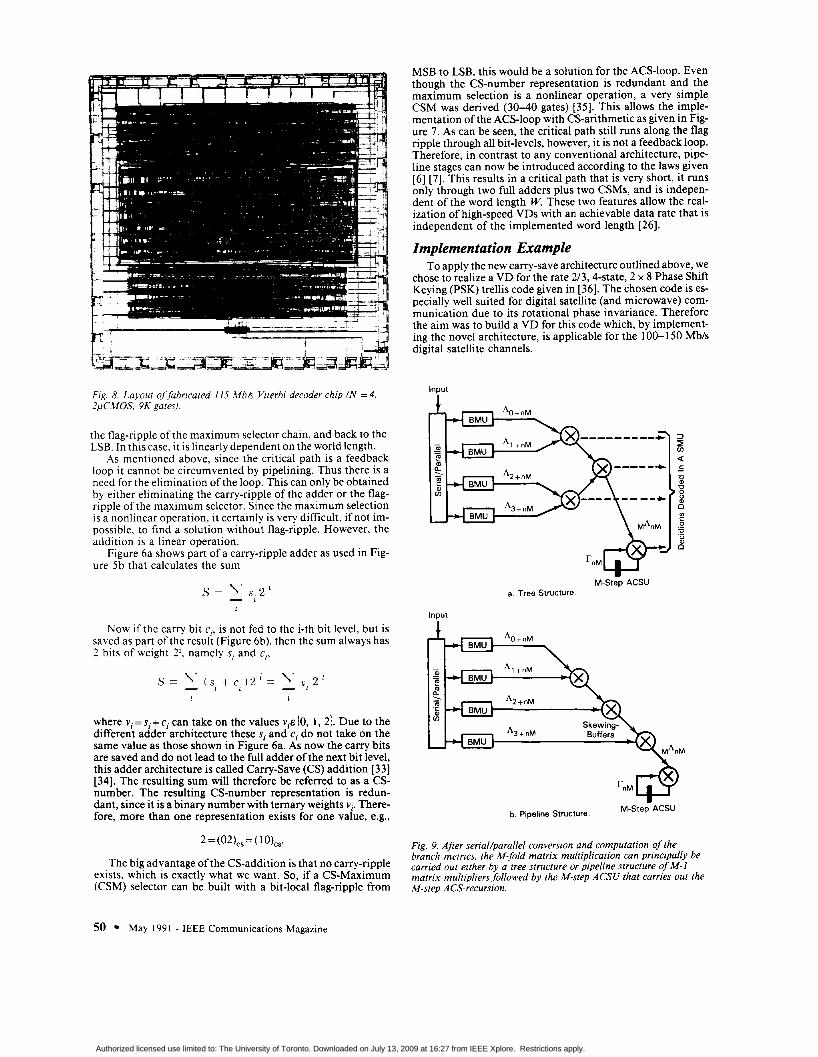
Fig. 8. Layout of fabricated 115 Mbh Viterbi decoder chip (N = 4, 2pC.WOS. 9K gates).
the flag-ripple of the maximum selector chain, and back to the LSB. In this case, it is linearly dependent on the world length.
As mentioned above, since the critical path is a feedback loop it cannot be circumvented by pipelining. Thus there is a need for the elimination of the loop. This can only be obtained by either eliminating the carry-ripple of the adder or the flag- ripple of the maximum selector. Since the maximum selection is a nonlinear operation, it certainly is very difficult, if not im- possible, to find a solution without flag-ripple. However, the addition is a linear operation.
Figure 6a shows part of a carry-ripple adder as used in Fig- ure 5b that calculates the sum
Now if the carry bit c,, is not fed to the i-th bit level, but is saved as part of the result (Figure 6b), then the sum always has 2 bits of weight 2', namely s, and c,,
s = '- ( s + c 1 ) 2 ' = v , 2 ' - 1
I 1
where vi=si+ci can take on the values vi& (0, 1, 21. Due to the different adder architecture these si and ci do not take on the same value as those shown in Figure 6a. As now the carry bits are saved and do not lead to the full adder of the next bit level, this adder architecture is called Carry-Save (CS) addition [33] [34]. The resulting sum will therefore be referred to as a CS- number. The resulting CS-number representation is redun- dant, since it is a binary number with ternary weights vi' There- fore, more than one representation exists for one value, e.g.,
2 = (02),, = ( 1 o)cs, The big advantage of the CS-addition is that no carry-ripple
exists, which is exactly what we want. So, if a CS-Maximum (CSM) selector can be built with a bit-local flag-ripple from
50 May 1991 - IEEE Communications Magazine
MSB to LSB, this would be a solution for the ACS-loop. Even though the CS-number representation is redundant and the maximum selection is a nonlinear operation, a very simple CSM was derived (30-40 gates) (351. This allows the imple- mentation of the ACS-loop with CS-arithmetic as given in Fig- ure 7. As can be seen, the critical path still runs along the flag ripple through all bit-levels, however, it is not a feedback loop. Therefore, in contrast to any conventional architecture, pipe- line stages can now be introduced according to the laws given [6] [7]. This results in a critical path that is very short, it runs only through two full adders plus two CSMs, and is indepen- dent of the word length W. These two features allow the real- ization of high-speed VDs with an achievable data rate that is independent of the implemented word length [26].
Implementation Example To apply the new carry-save architecture outlined above, we
chose to realize a VD for the rate 213, 4-state, 2 x 8 Phase Shift Keying (PSK) trellis code given in [36]. The chosen code is es- pecially well suited for digital satellite (and microwave) com- munication due to its rotational phase invariance. Therefore the aim was to build a VD for this code which, by implement- ing the novel architecture, is applicable for the 100-1 50 Mbls digital satellite channels.
Input
'O+nM
U
- '1 +nM 2 4 BMU 1 2
'3 + nM
M-Step ACSU a. Tree Structure.
Input
'0 + nM
'2 + nM
"1 I -. Skewing-
'3+nM Buffers
b. Pipeline Structure. M-Step
Fig. 9. After serial/parallel conversion and computation of the branch metrics, the M-fold matrix multiplication can principally be carried out either by a tree structure or pipeline structure of M-I matrix multipliers followed by the M-step ACSU that carries out the M-step ACS-recursion.
Authorized licensed use limited to: The University of Toronto. Downloaded on July 13, 2009 at 16:27 from IEEE Xplore. Restrictions apply.
structure called a semi-ring [35] [37-391. Using these symbols we can write the ACS-recursion of Equation 1 as
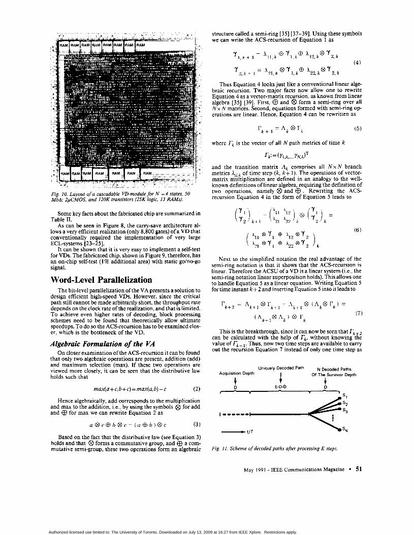
Fig. 10. Layout of a cascadable VD-module for N = 4 states, SO M b h ZpCMOS, and 120K transistors (2SK logic, 13 RAMS).
Some key facts about the fabricated chip are summarized in Table 11.
As can be seen in Figure 8, the carry-save architecture al- lows a very efficient realization (only 8,800 gates) of a VD that conventionally required the implementation of very large ECGsystems [23-251.
It can be shown that it is very easy to implement a self-test for VDs. The fabricated chip, shown in Figure 9, therefore, has an on-chip self-test (1% additional area) with static go/no-go signal.
Word-Level Parallelization The bit-level parallelization of the VA presents a solution to
design efficient high-speed VDs. However, since the critical path still cannot be made arbitrarily short, the throughput rate depends on the clock rate of the realization, and that is limited. To achieve even higher rates of decoding, block processing schemes need to be found that theoretically allow ultimate speedups. To do so the ACS-recursion has to be examined clos- er, which is the bottleneck of the VD.
Algebraic Formulation of the VA On closer examination of the ACS-recursion it can be found
that only two algebraic operations are present, addition (add) and maximum selection (max). If these two operations are viewed more closely, it can be seen that the distributive law holds such that
max(a + c, b+ c) = max(a, b) + c (2)
Hence algebraically, add corresponds to the multiplication and max to the addition, i.e., by using the symbols @ for add and @ for max we can rewrite Equation 2 as
a € 3 c @ 6 € 3 c = ( a @ h ) @ c (3 1
Based on the fact that the distributive law (see Equation 3) holds and that @ forms a commutative group, and @ a com- mutative semi-group, these two operations form an algebraic
Thus Equation 4 looks just like a conventional linear alge- braic recursion. Two major facts now allow one to rewrite Equation 4 as a vector-matrix recursion, as known from linear algebra [35] [39]. First, @ and @ form a semi-ring over all N x N matrices. Second, equations formed with semi-ring op- erations are linear. Hence, Equation 4 can be rewritten as
I., + = Ak €3 I', (5 1
where r k is the vector of all N path metrics of time k
rk: = (rl ,k ,..., YN,k)T
and the transition matrix Ak comprises all N x N branch metrics Lijk of time step (k, k+ 1). The operations of vector- matrix multiplication are defined in an analogy to the well- known definitions of linear algebra, requiring the definition of two operations, namely @ and @ . Rewriting the ACS- recursion Equation 4 in the form of Equation 5 leads to
Next to the simplified notation the real advantage of the semi-ring notation is that it shows that the ACS-recursion is linear. Therefore the ACSU of a VD is a linear system (i.e., the semi-ring notation linear superposition holds). This allows one to handle Equation 5 as a linear equation. Writing Equation 5 for time instant k+ 2 and inserting Equation 5 into it leads to
This is the breakthrough, since it can now be seen that r k can be calculated with the help of r, without knowing t i e value of r,+ Thus, now two time steps are available to carry out the recursion Equation 7 instead of only one time step as
Uniquely Decoded Path N Decoded Paths Of The Survivor Depth I t
Acquisition Depth
E-D-D 1
r T 7
Fig. 11. Scheme of decoded paths afer processing E steps.
May 1991 - IEEE Communications Magazine 51
Authorized licensed use limited to: The University of Toronto. Downloaded on July 13, 2009 at 16:27 from IEEE Xplore. Restrictions apply.
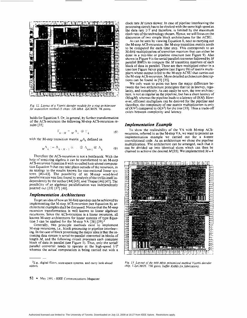
Fig. 12. Layout of a Viterbi decoder module for a ring architecture for acquisition method (5 chips: 120 Mbh. 2pCM0.9, 9K gates).
holds for Equation 5. Or, in general, by further transformation of the ACS-recursion the following M-step ACS-recursion re- sults [35]
with the M-step transition matrix MAk defined as
Therefore the ACS-recursion is not a bottleneck. With the help of semi-ring algebra it can be transformed to an M-step ACS-recursion Equation 8 with so-called look-ahead computa- tion Equation 9 that can take place outside of the recursion, in an analogy to the results known for conventional linear sys- tems [40-431. The possibility of an M-step word-level parallelization was first found by analysis of the trellis itself in- dependently by the author [44] [45], and Thapar [46] [47]. The possibility of an algebraic parallelization was independently pointed out [35] [37] [48].
Implementation Architectures To get an idea of how an M-fold speedup can be achieved by
implementing the M-step ACS-recursion (see Equation 8), ar- chitectural examples shall be discussed. Notice that the M-step recursion transformation is well known to linear algebraic recursions. Since the ACS-recursion is a linear recursion, all known M-step architectures for linear systems o f t pe Equa-
Generally, two principle methods exist to implement M-step recursions, i.e., block processing or pipeline interleav- ing. In the case of block processing the major idea is that the in- coming data stream is serial-to-parallel converted in blocks of length M , and the following circuit processes each complete block of data in parallel (see Figure 1). Thus, only the seriall parallel converter needs to operate at the high-speed 1/T whereas the actual computation is being carried out with a
tion 5 can be applied for the M-step VA [38] [39]. z
clock rate M times slower. In case of pipeline interleaving the processing circuit has to be clocked with the same high speed as the data rate 1/T and therefore, is limited by the maximum clock rate of the technology chosen. Hence, we will focus on the discussion of two simple block architectures for the ACSU.
As can be seen by viewing Equation 8, next to carrying out the M-step ACS-recursion, the M-step transition matrix needs to be computed for each time step. This corresponds to an M-fold multiplication of transition matrices that can either be done in a tree-like or pipeline structure (see Figure 9). Also shown in Figure 9 is the serial/parallel converter followed by M parallel BMus to compute the M transition matrices of each block of data in parallel. These are then multiplied either in a tree (see Figure 9a) or pipeline (see Figure 9b) of matrix multi- pliers whose output is fed to the M-step ACSU that cames out the M-step ACS-recursion. More detailed architecture descrip- tions can be found in [9] [35].
We only want to point out here the major difference be- tween the two architecture principles that lie in latency, regu- larity, and complexity. As can easily be seen, the tree architec- ture, is not as regular as the pipeline, but has a short latency of O(logM), whereas the pipeline leads to a latency of O(M). How- ever, efficient multipliers can be derived for the pipeline and therefore, the complexity of one matrix multiplication is only of O ( N 3 compared to O(N3) for the tree [35]. Thus a trade-off exists between complexity and latency.
Implementation Example To show the realizability of the VA with M-step ACS-
recursion, referred to as the M-step VA, we want to present an implementation example we carried out for a 4-state convolutional code. As an architecture we chose the pipeline multiplication. The architecture can be arranged, such that it can be divided up into identical slices which can then be chained to achieve the desired M [35]. We implemented M= 4
2E.g., digital filters, state-space systems, and carry look-ahead Fig. 13. Layout of the 600 Mbb minimized method Viterbi decoder chip, I.ZpCMOS, 75K gates, buffer RAMS (in fabrication). adders.
52 May 199 1 - IEEE Communications Magazine
Authorized licensed use limited to: The University of Toronto. Downloaded on July 13, 2009 at 16:27 from IEEE Xplore. Restrictions apply.
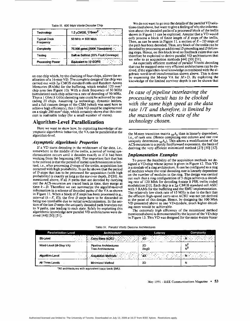
Table 111. 600 Mb/s Viterbi Decoder Chip
50 MHz 3 600 Mbls
on one chip which, by the chaining of four chips, allows the re- alization of a 16-step VD. The complete design of the chip was camed out with 2p CMOS standard cells and Random Access Memories (RAMs) for the buffering, which totaled 120 mm2 chip area (see Figure 10). With a clock frequency of 50 MHz (simulation) each chip achieves a rate of decoding of 50 MHz. Thus a 1 Gb/s (1 GHz) decoding rate could be achieved by cas- cading 20 chips. Assuming 1p technology, dynamic latches, and a full custom design of the CSM (which was used here to achieve high efficiency), this 1 Gb/s VD could be implemented on a single 200 mm2 chip, which certainly shows that this con- cept is realizable today (for a small number of states).
Algorithm-Level Parallelization Here we want to show how, by exploiting knowledge of as-
ymptotic algorithmic behavior, the VA can be paralleled at the algorithm-level.
Asymptotic Algorithmic Properties If a VD starts decoding in the midstream of the data, i.e.,
somewhere in the middle of the trellis, a period of initial syn- chronization occurs until it decodes exactly as if it had been working from the beginning [49]. The important fact that has to be noticed is that the period of initial synchronization is lim- ited, i.e., after processing D steps of the trellis, acquisition has occurred with high probability. It can be shown that the period of D steps that has to be processed for acquisition (with high probability) is exactly as long as the survivor depth, D [50]. As mentioned above, if all N paths that are decoded by carrying out the ACS-recursion are traced back in time, they merge at time k-D. Therefore we can summarize the algorithm-level information in a scheme of decoded paths of the VA as shown in Figure 1 1. When a block of E steps has been processed (e.g., interval ( k -E , E)), the first D steps have to be discarded as being too unreliable due to initial synchronization. In the sec- tion of the last D steps the uniquely decoded path branches out to N paths, one leading to each state. Solely by exploiting this algorithmic knowledge new parallel VD architectures were de- rived [44] [50] [51].
We do not want to go into the details of the parallel VD solu- tions cited above, but want to give a feeling ofwhy the informa- tion about the decoded paths of a processed block of the trellis shown in Figure 1 1 can be exploited. Assume that a VD would only process a block of finite length of E steps of the trellis. Then, as can be seen in Figure 1 1, a section of E - 2 0 steps of the path has been decoded. Thus, any block of the trellis can be decoded by processing an additional D preceding and D follow- ing steps. Hence, on this block level no feedback exists that can therefore be exploited to derive parallel VD architectures that we refer to as acquisition methods [44] [50] [51].
An especially efficient method of parallel Viterbi decoding that can be mapped onto very efficient architectures can be de- rived, ifthe algorithm-level knowledge is combined with the al- gebraic word-level transformation shown above. This is done by examining the M-step VA for M > D . By exploiting the knowledge of the limited survivor depth it can be shown that
In case of pipeline interleaving the processing circuit has to be clocked with the same high speed as the data rate U T and therefore, is limited by the maximum clock rate of the tech nology chosen.
the M-step transition matrix MAP than is linearly dependent, i.e., of rank one. (Hence computing one column and one row uniquely determines ,Ak). This allows a modification of the ACS-recursion to a purely feedforward expression, the basis of deriving the very efficient minimized method [27] [50] [52].
Implementation Examples To prove the feasibility of the acquisition methods we de-
signed a VD-chip whose layout is given in Figure 12. This VD is a module of a ring architecture. It can be configured to a ring of modules where the total decoding rate is linearly dependent on the number of modules in the ring. The design was camed out such that a ring configuration of 5 chips achieves a decod- ing rate of 120 Mbls for decoding 6-state 8 PSK trellis coded modulation [53]. Each chip is a 2p CMOS standard cell ASIC with 5 RAMs for the buffering and the SMU implementation. The relatively low clock rate of 15 MHz is due to the fact that the efficient high-speed carry-save ACSU was not yet derived at the point of this design. Hence, by designing the 100 Mb/s VD presented above as one VD-module, much higher decod- ing rates would be achievable.
The extremely high efficiency of the minimized method mentioned above is demonstrated by the layout of the VD chip in Figure 13. This VD was designed for the same 4-state linear
Table IV. Parallel Viterbi Decoder Architectures
Cany-Save ACSU 1
All Three Levels Minimized Method
*All architectures with equivalent trace-back SMU.
May 1991 - IEEE Communications Magazine 9 53
Authorized licensed use limited to: The University of Toronto. Downloaded on July 13, 2009 at 16:27 from IEEE Xplore. Restrictions apply.
convolutional code (constraint length K = 3) that underlines the chip design shown above (see Figure 9). The chip is de- signed with l .2p standard cells and 3 RAMS for buffering and consumes 170 mm2 chip area. Taking into account a minimum clock frequency of 50 MHz and the fact that a block of D = 12 steps is decoded per chip in parallel, results in a decoding rate per chip of at least 600 Mb/s. This is already more than 20 times the rate of the fastest commercial VD chip available to date [22] (see Table I). Some key facts of the chip which is cur- rently being sent to fabrication are given in Table 111.
The minimum system configuration, which needs 2 chips, achieves 1.2 Gb/s, and multiples hereof are obtained by using more chips in parallel.
Conclusions For very high throughput rates not only the inherent paral-
lelism of an algorithm needs to be extracted, but additional parallelism has to be introduced. For this sake three levels exist, namely the bit-, word-, and algorithm-level.
Even though the ACS-recursion presents a bottleneck for high-speed implementations of the Viterbi algorithm, addi- tional parallelism can be introduced at all three levels. At the bit-level the derivation of nonlinear carry-save arithmetic al- lows pipelining the ACS-recursion between the bit-levels, such that the critical path is extremely short and independent of the word-length. At the word-level the two operations of the ACS- recursion were identified to form an algebraic structure that al- lowed an algebraic transformation such that the bottleneck was eliminated. Finally, at the algorithm-level asymptotic behavior was exploited to derive parallel processing architectures. Fur- thermore, it was pointed out that by combining the word- and algorithm-level, a very efficient minimized method can be de- rived which, when the bit-level carry-save optimizations are used, allows the realization of Viterbi decoders up to the Gbls range on one chip in present-day technologies.
The different solutions span a wide space, as is summarized in Table IV. To achieve an extremely small latency one has to pay by increased complexity of O(N3) (tree architecture) whereas the combination of all three levels (minimized meth- od) is a good compromise between latency and complexity.
The Viterbi algorithm is only one specific example of a large set of algorithms which is of interest to design parallel process- ing architectures. Therefore, it is important to derive metho- dologies and tools of how to introduce additional parallelism into algorithms. The basic tools applied here were CS- arithmetic at the bit-level, semi-ring algebra at the word-level, and exploiting acquisition properties at the algorithm-level. We believe that the generalizations of all three methods of finding solutions at each level are a step in this direction [9]. However, a lot of work remains to be done.
Acknowledgment The authors want to thank numerous students that helped
designing the VLSI case studies, and especially Herbert Dawid for carrying out the majority of the design work for the 600 Mbls chip.
References [ l ] R Karp. Miller and S Winograd, -The Organization of Computations
for Uniform Recurrence Equations," J ACM, vol 14, pp 563-590, 1967 S Kung, VLSlprocessorarrays, Englewood Cliffs Prentice Hall, 1987 L Thiele. "On The Hierarchical Design of VLSl Processor Arrays," Proc ISCAS, pp 2517-2520, Helsinki, 1988 S Rao and T Kailath. "Regular Iterative Algorithms and Their Imple- mentation on Processor Arrays," Proc IEEE, vol 76, pp 215-234, Mar 1988
[2] [3]
[4]
[51
[91
D. Moldovan, "Towards a Computerized Optimal Design of VLSl Sys- tolic Arrays," Design Methodologies, Elsevier Science Publ., pp. 21 5- 234, 1986. A. Fettweis, 'Realizability of Digital Filter Networks," Elect. and Commun. (AEU). vol. 30, pp. 90-96, 1976. C. Leiserson and J. Saxe, "Optimizing Synchronous Systems," J. of VLSland Computer Systems. vol. 1, pp. 41-67, 1983. G. Fettweis and H. Meyr, "On the Interaction Between DSP-Algorithm and VLSCArchitecture," Proc. IEEE lnt% Zurich Seminar on Digital Commun., pp. 219-230, Zurich, Switzerland, Mar. 1990. G. Fettweis, 'Parallelisierung des Viterbi Decoders: Algorithmus and VLSI-Architektur," VDE Forfschrinsberichte, Reihe l o . , vol. 144, ISBN 3-18-144410-3 Dusseldorf, FRG: VDE-Verlag, 1990. R. Bellman and S. Dreyfus, Applied dynamic programming, Princeton NJ: Princeton University Press, 1962. A. Omura, 'On the Viterbi Algorithm," IEEE Trans. Info. Theory. pp. 177-179, Jan. 1969. A. Viterbi, "Error Bounds for Convolutional Coding and an Asymptoti- cally Optimum Decoding Algorithm," IEEE Trans. Info. Theory, vol. IT- 13, pp 260-269, Apr. 1967 G. Forney. 'The Viterbi Algorithm," Proc. IEEE, vol. 61, pp. 268-278, Mar. 1973. H. D. Lin and D. Messerschmitt, "Architectures for Viterbi Decoding and ML Estimators for Controllable Markov Sources," tech. rep., Uni- versity of California, Berkeley, CA, 1988. H.D. Lin and D. Messerschmitt, "Algorithms and Architectures for Concurrent Viterbi Decoding," IEEEICC, vol. 2, pp. 836-840, Boston, MA, June 1989. J. Snyder, "High Speed Viterbi Decoding of High Rate Codes," 7th ICDSC, pp. XI1 16-23, Phoenix, AZ, Sept. 1983. H. Stone, "Parallel Processing With the Perfect Shuffle," IEEE Trans. on Computers, vol. C-20. pp, 153-161, Feb. 1971. H. Burkhardt and L. Barbosa, 'Contributions to the Application of the Viterbi Algorithm," IEEE Trans. Info. Theory, vol. IT-3 1, pp. 626-634, Sept. 1985. P. Gulak and T. Kailath, 'Locally Connected VLSl Architectures for the Viterbi Algorithm," IEEEJ. on Se/. Areasin Commun.. vol. SAC-6, pp. 527-537, Apr. 1988. J. Stahl, M. Oerder, and H. Meyr, 'Implementation of a High Speed Viterbi Decoder," Signal Processing / / I . TheoryandApplications, I. e. a. Young, Ed., North-Holland. Elsevier Science Publ. 8.V.. pp. 1 1 17- 1120, 1986. S. Kubota and S. Kato, "Viterbi Decoder VLSl Implementation and Its Applications," Abstracts and Papers of IEEE lnt'l. Workshop Microelectronics and Photonics in Commun., pp. lI.l.1-8. Cape Cod MA, June 1989. S. Kubota etal., "Compact, High-speed and High-Coding-Gain General Purpose FEC EncoderIDecoder-NUFEC code-," Proc. ICC, pp. 798- 803 (25.3.1-6). Boston MA, June 1989. T. Fujino etal., "A 120 Mb/s Coded 8PSK Modem With Soft-Decision Viterbi Decoder," Proc. ICC, pp. 1774-1 780, Toronto, 1986. R. Fang, "A Coded 8 MHz System for 140 Mb/s Information Rate Transmission Over 80 MHz Nonlinear Transponders," ICDSC, pp.
T. Suzuki and Y. Saitoh, "A 100 Mb/s Optical Transmission Experi- ment Employing a Viterbi Decoder Composed of Analog Circuits," Proc. ISSSE, pp, 156-158, Erlangen FRG, 1989. G. Fettweis and H. Meyr, "A 100 Mb/s Viterbi-Decoder Chip: Novel Architecture and Its Realization," Proc. ICC, vol. 2, pp. 463-467 (307 4), Atlanta, GA, Apr. 1990 G. Fettweis, H. Dawid, and H. Meyr, "Minimized Method Viterbi De- coding: 600 Mb/s per Chip,- Proc. GLOBECOM. vol. 3, pp. 1712- 1716 (808.5). San Diego, CA, Dec. 1990. S. Kubota, K. Ohtani, and S. Kato, "High-speed and High-Coding-Gain Viterbi Decoder with Low Power Consumption Employing Scarce State Transition (SST) Scheme," Elect. Len., vol. 22, pp. 491-493, Apr 1986. Qualcomm Inc , San Diego, CA, Viterbi Decoder on Single Chip, K= 7 Rate 112. Oct. 1988. Stanford Telecommunications. Santa Clara, CA, 20 Mbb convolutional encoder Viterbi decoder - STEL 2020, Oct. 1989. Qualcommlnc., SanDiego, CA, TheQ1650C-3L ViterbiCodec, 1991. G. Fettweis and H. Meyr, "Ein 100 Mbls Viterbi Decoder Chip: Architektur und Realisierung," Proc. ITG-Conf Mikmelektronik fur die Kommunikationstechnik, pp. 163-168, ITG-Fachbericht 1 10, Stutrgart FRG, Oct. 1989. 0. Spaniol, 'Arithmetik in Rechenanlagen," Studienbucher lnformatik. vol. 34, Teubner, 1976. K. Hwang and F. Briggs, ComputerArchitecture and Parallel Processing. McGraw-Hill, 1985. G. Fettweis and H. Meyr, 'High-speed Viterbi Processor: A Systolic Array Solution," IEEE J. on Se/. Areas in Commun., vol. SAC-8, pp.
G. Fettweis, "New rotationally invariant trellis codes for 8PSK modula- tion." Proc. IEEEICC, vol 3, pp. 1388-1392 (45.6). Boston MA, June 1989.
305-313, 1986.
1520-1 534, Oct. 1990.
54 May 199 I - IEEE Communications Magazine
Authorized licensed use limited to: The University of Toronto. Downloaded on July 13, 2009 at 16:27 from IEEE Xplore. Restrictions apply.
G. Fettweis and H. Meyr, 'A Systolic Array Viterbi Processor for High Data Rates,' SystolicAmy Processors, J. McCanny, J. McWirther, and E. Swartzlander, Eds., Prentice Hall, pp. 195-204, June 1989. G. Fettweis, L. Thiele, and H. Meyr, 'Algorithm Transformations for Unlimited Parallelism,' Proc. IEEE Int'l. Symp. on Circuits and Systems, vol. 2, pp. 1756-59, New Orleans LA, May 1990. L. Thiele and G. Fettweis, 'Algorithm Transformations for Unlimited Parallelism,' Elect. and Commun. (AEU), pp. 83-91, Apr. 1990. P. Kogge and H. Stone, 'A Parallel Algorithm For the Efficient Solution of a General Class of Recurrence Equations,' IEEE Trans. on Computers,
R. Keller, 'Look-Ahead Processors," Compuhg Sutveys. vol. 7. pp.
R. Ladner and M. Fisher, 'Parallel Prefix Computation,' J. of the ACM,
K. Parhi and D. Messerschmidt, 'Block Digital Filtering Via Incremental Block-State-Structures.' Proc. IEEE lnt% Symp. on Circuits and Sys- tems. pp. 645-648, Philadelphia, 1987. G. Fettweis, 'Verfahren zur Ausfurung des Viterbi-Algorithmus mit Hilfe Parallelverarbeitender Strukturen," German Pat. pend., July 1987. G. Fettweis and H. Meyr, 'Parallel Viterbi Algorithm Implementation: Breaking the ACS-Bottleneck,' IEEE Trans. on Commun.. vol. COM-37,
H. Thapar, 'Application of Block Processing to the Design of High- Speed Viterbi Detectors,' tech, rep., IBM, San Jose, CA, Dec. 1986. H. Thapar and J. Cioffi, -A Block Processing Method for Designing High-speed Viterbi Detectors," Proc. IEEEICC, vol. 2, pp. 1096-1 1 0 0 (35.5). Boston, MA, June 1989. K. A. Wen and J. Y. Lee, 'Parallel Processing for Viterbi Algorithm,' Elect. Lett.. vol. 24, pp. 1098-99. Aug. 1988. A. Viterbi and A. Omura, Principles of Digital Communications. McGraw-Hilll, 1979. G. Fettweis and H. Meyr. 'Feedforward Architectures for Parallel Viterbi Decoding,'acceptedforKluwerJ. on VLSlSignalproCessing, no.
G. Fettweis and H. Meyr, 'A Modular Variable Rate Viterbi Decoding Implementation for High Data Rates,' Signal Processing 1 K Theores andApplications, J. L. Lacoume et at., Eds., Proc. EUSIXO '88vol. 1. pp. 339-342, Elsevier Science Publishers, North-Holland, 1988.
vol. C-22, pp. 786-793, 1973.
177-195, 1975.
VOI. ACM 27, pp. 831-838, 1980.
pp. 785-790, Aug. 1989.
3, pp. 105-1 19, 1991.
(521 G. Fettweis and H. Meyr, 'Cascaded Feedforward Architectures for Parallel Viterbi Decoding,' Proc. IEEE ISCAS, vol. 2, pp. 1756-59, New Orleans LA, May 1990. M. Oerder and H. Meyr, 'Rotationally Invariant Trellis Codes for MPSK Modulation,' Elect. and Commun. (AEU). vol. 41, pp. 28-32, 1987.
(531
Biography Gerhard Fettweis is a visiting scientist at the IBM Almaden Research Cen-
ter, San Jose, California. He received his Dipl. -Ing. and Ph.D. degree from the Aachen University of Technology, Aachen, Germany, in 1986 and 1990, re- spectively. During 1986 he worked at the Asea Brown Boveri (ABB) research laboratory, Baden, Switzerland, on his Diplom-thesis.
His interests are in microelectronics and digital communications, especially the interaction between algorithm and architecture design for VLSl implemen- tations.
Heinrich Meyr received the Dipl.-lng. and Ph.D. degrees from the Swiss Federal Institute of Technology (ETH), Zurich, Switzerland, in 1967 and 1973, respectively.
From 1968-1970 he held research positions at Brown Boveri Corporation, Zurich, and the Swiss Federal Institute for Reactor Research. From 1970 to the summer of 1977 he was with H a s h Research Laboratory, Bern, Switzerland. His last position at Hasler was Manager of the Research Department. During 1974 he was a visiting Assistant Professor with the Department of Electrical Engineering, University of Southern California, Los Angeles. Since the summer of 1977 he has been Professor of Electrical Engineering at the Aachen Univer- sity of Technology (RWTH), Aachen, West Germany. His research focuses on synchronization, digital signal processing, and in particular, on algorithms and architectures suitable for VLSl implementation. In this area he is frequently in demand as a consultant t o industrial concerns. He has published work in vari- ous fields and journals and holds over a dozen patents.
Mr. Meyr served as Vice Chairman for the 1978 IEEE Zurich Seminar and as an International Chairman for the 1980 National Telecommunications Confer- ence, Houston, TX. He served as Associate Editor for the IEEE Trans. on Acous- tics, Speech, andSignalProcesingfrom 1982-1985, end as Vice President for International Affairs of the IEEE Communications Society.
SOREP TECHNOLOGY Corp. : v i m i DECODERS
.A,
'2 0 - D
a .. - S T A N D A R D P R O D U C T D I V I S I O N 2248-BSchlumbergerrtreet-HOUSTONTEXAS, 77023USA-Tel 1117139235200 Fax 11)7139234182
Circle number 13
May 1991 - IEEE Communications Magazine 55
Authorized licensed use limited to: The University of Toronto. Downloaded on July 13, 2009 at 16:27 from IEEE Xplore. Restrictions apply.