High Speed Circuits That Work - web.stanford.edu
18
EE 371 lecture 15 1 High Speed Circuits That Work: The Road From Ideas to Products EE 371 Lecture 15 Sam Naffziger Hewlett Packard Co. EE 371 lecture 15 2 Overview • Goal: Provide some insight into the design process for high speed circuits taken from concept to customer ship • I’ll use a block on the soon-to-ship McKinley (Itanium® 2) microprocessor as a case study – What motivated and supported some of the circuit innovation – What the design process involved – Some of the issues that arose – How the silicon actually behaved • The 1 st level data cache (L1D) is a great example – 16KB, 4 way set associative, physically tagged, 1 cycle load to use (0 cycle penalty) • But first, some background on the microprocessor ($$) (blood, sweat and tears) (weeping and gnashing of teeth) (very un-SPICE-like)
Transcript of High Speed Circuits That Work - web.stanford.edu

1
EE 371 lecture 15 1
High Speed Circuits That Work: The Road From Ideas to Products
EE 371 Lecture 15Sam Naffziger
Hewlett Packard Co.
EE 371 lecture 15 2
Overview• Goal: Provide some insight into the design process for
high speed circuits taken from concept to customer ship
• I’ll use a block on the soon-to-ship McKinley (Itanium® 2) microprocessor as a case study– What motivated and supported some of the circuit innovation – What the design process involved– Some of the issues that arose– How the silicon actually behaved
• The 1st level data cache (L1D) is a great example– 16KB, 4 way set associative, physically tagged, 1 cycle load
to use (0 cycle penalty) • But first, some background on the microprocessor
($$)(blood, sweat and tears)(weeping and gnashing of teeth)(very un-SPICE-like)

2
EE 371 lecture 15 3
Bus Logic
CLK
L1Dcache
Integer Datapath
DTLB
L3 TagL2D Array and Control
ALAT
HPW
Pipeline Control
Floating Point UnitBranch Unit
L1Icache
IA32
L3 Cache
IntRF
Multi-Mediaunit
McKinley Overview• .18µm bulk, 6 layer Al
process• 8 stage, fully stalled in-
order pipeline• Symmetric six integer-
issue design• IA32 execution engine
integrated• 3 levels of cache on-die
totaling 3.3MB• 221 Million transistors• ECC / parity protection
on all memory arrays• 130W @1GHz, 1.5V 19.5mm
21.6
mm
EE 371 lecture 15 4
McKinley vs. other 64b .18µm processors(sources provided in final slide)
12 (~11)9 (~11)14 (8)8 (6)Pipe stages (mpb)
12512575130Power (Watts)
100 est.115206142Core size (no IO, only lowest level caches)
400 est.397244421Die size (mm2)41.6 / core19.216.864GB/sD Cache read BW
1.7MB2.5 per core
1.8MB3 arrays
96KB2 arrays
3.3MB4 arrays
On chip cache2/cycle2/cycle2/cycle2/cycleFP units3/cycle4/cycle3 / cycle6 / cycleSustainable Int BW
1.31.0-1.21.051.0Frequency (GHz)
Power 4(2 cores)
EV7USIIIMcKinley

3
EE 371 lecture 15 5
Background• Memory access is a very important aspect of processor design
– Bandwidth must support full instruction streaming– Latency must be low enough to minimize pipeline stalls
• Contemporary processors have a 1-2 cycle load to use penalty for the 1st level cache. I.e. LD addr→A followed by Add A,B incurs a stall
• Lately, most microprocessors have embraced out of order execution (PA, Power4, Alpha, Pentium)
– Can do useful work even if the main pipe is stalled– Can significantly mitigate cache latency impacts
• Witness the PA8700 with a 1.5MB first level data cache. Latency is 3 cycles, but more than offset by the benefits of the large cache
• BUT, the Itanium architecture is resistant to out of order implementations
– The whole template based instruction format– Worse, ubiquitous predicates – any instruction can be predicated off
EE 371 lecture 15 6
Background: Predication
cmpcmp
p1
p1
p1
p2
p2
p2
Traditional ArchitecturesTraditional Architectures IAIA--6464
• Removes branches, converts to predicated execution – Executes multiple paths simultaneously
• Increases performance by exposing parallelism and reducing critical path – Better utilization of wider machines– Reduces mispredicted branches
elseelse
thenthen
cmpcmp
4
EE 371 lecture 15 7
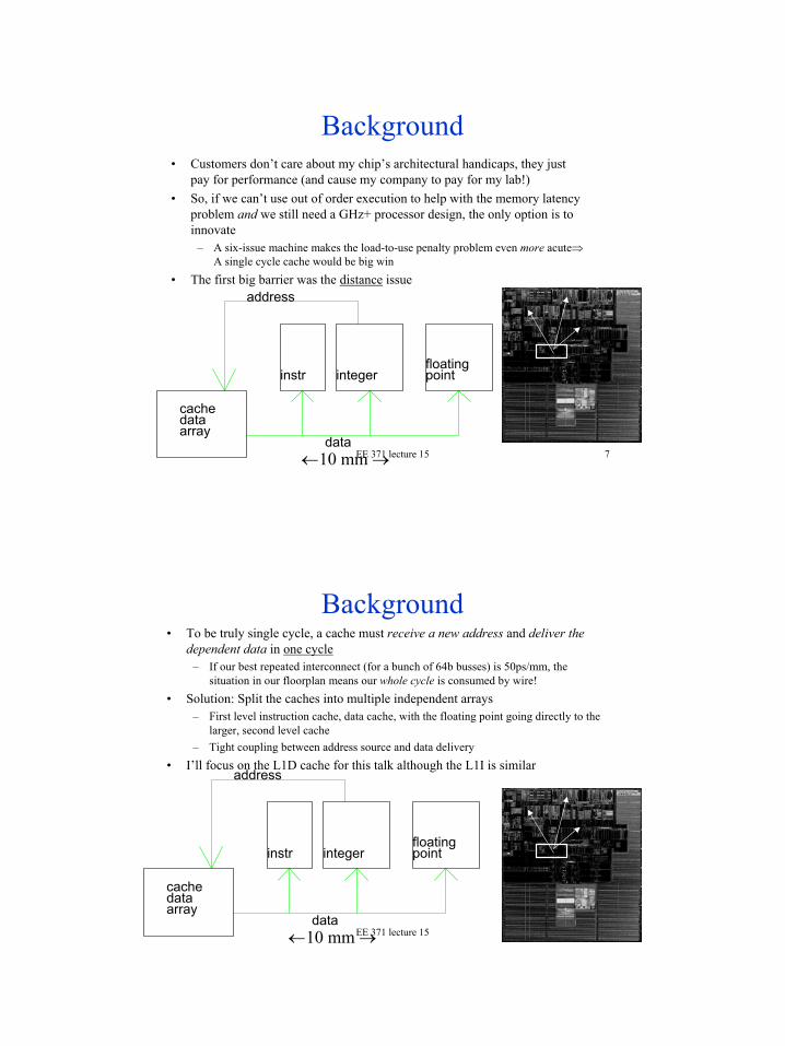
Background• Customers don’t care about my chip’s architectural handicaps, they just
pay for performance (and cause my company to pay for my lab!)• So, if we can’t use out of order execution to help with the memory latency
problem and we still need a GHz+ processor design, the only option is to innovate
– A six-issue machine makes the load-to-use penalty problem even more acute⇒A single cycle cache would be big win
• The first big barrier was the distance issueaddress
data
pointfloating
integerinstr
arraydatacache
←10 mm →
EE 371 lecture 15 8
Background• To be truly single cycle, a cache must receive a new address and deliver the
dependent data in one cycle– If our best repeated interconnect (for a bunch of 64b busses) is 50ps/mm, the
situation in our floorplan means our whole cycle is consumed by wire!• Solution: Split the caches into multiple independent arrays
– First level instruction cache, data cache, with the floating point going directly to the larger, second level cache
– Tight coupling between address source and data delivery• I’ll focus on the L1D cache for this talk although the L1I is similar
address
data
pointfloating
integerinstr
arraydatacache
←10 mm →

5
EE 371 lecture 15 9
Cache Access Timing• High speed caches usually take the following form (only for latency insensitive
or very power sensitive designs does the data array access wait on the tag)• If a cycle time is only 20-24 FO4 inverters, this is a lot to get done
– The TLB access is a problem – wide CAM + RAM access– 38 bits is a lot to compare– Just the way mux, data massage and deliver is generally a full cycle …
Data delivery
Compare
DATA
TAG
TLB
Dat
a M
assa
ge
mux
Fina
l dat
a
Way
mux
Addr
ess
mux
38 bits!
VA[63:0]
PA[49:0]
64b X ways
EE 371 lecture 15 10
Cache Access Timing• So, I set out to attack the following areas:
– TLB access + TAG compare• 76 bit CAM, followed by a RAM access followed by a 38b compare• Then buffer up the compare result to drive the way multiplexors for a 64b datapath
– Way mux + data massage (this is way harder than you might think) + delivery• Must deliver either big or little endian data, must zero extend sub-word loads, must align
subword loads, must bypass store data in and merge it with load data!– Data array access – speed enables a larger cache
• Timing should match TLB/TAG plus compare
• With only a single cycle to work with, I only get one clock edge!– If I use the falling edge clock, I’m victimized by phase asymmetries, as well as clock
skew which has its impact doubled for phase budgets (bad)– Everything must be either self-timed or dataflow => domino
Data delivery
Compare
DATA
TAG
TLB
Dat
a M
assa
ge
mux
Fina
l dat
a
Way
mux
Addr
ess
mux

6
EE 371 lecture 15 11
Level 1 TLB Overview• Takes a 64b Virtual address in, compares to stored
translations and generates a physical translation• 32 Entries, each of which stores 115 bits
• Fixed 4 kB page size• 2 independent CAM ports, each with shared CAM
lines for both virtual and physical address CAMs– This saves wires in the critical dimension
• 2-level dynamic CAM with a self timed path to create a monotonic-rising match signal.
– 52 virtual address bits– 38 physical address bits
– 24 Region ID bits– 1 Valid bit
EE 371 lecture 15 12
Level 1 TLB Pulsed Bit Lines
• The virtual address is presented to the CAM cell on a pair of dual-rail pulsed bit lines.
• Pulsed bit lines eliminate precharge drive fights and allow for the removal of clocked evaluate FETs on downstream dynamic gates.
I
I
I
II
I OO
Enable
NBIT
Addr
PCK BITPCK
Addr
Enable

7
EE 371 lecture 15 13
I
I
I
I
I
I
I
match1
cam0lcam0h
bit0h
write
bit0l
cam1lcam1h
match0
Level 1 TLB CAM Cell• One write port +2 CAM ports• CAM bit lines are pulsed• Cell discharges match[01]
when its value does notmatch the incoming address
• Cell layout is 27.3 µm2
(4.8 × standard RAM cell)• Stability is not an issue,
since the pass-fets onlyturn on during a write.
• Charge sharing is not anissue since 3 of every 4 pulldown stacks don’t evaluate.
EE 371 lecture 15 14
Level 1 TLB Self-Timed Path• CAM is wide (90 address bits × 2 pulldown stacks per cell)• We use a full-rail hierarchical dynamic structure for speed.
6 CAM cells → 2-input NAND → 4-wide OR → 2-input NAND• The TLB calculates a monotonic-falling match signal, but the TAG
needs a monotonic-rising match signal. Thus, a “dummy” self-timed path is used to create a hard edge.
• The “Johnson NOR” is used to account for PVT and clock route variations between the two halves of the TLB.
• The self-timed path consumes 20% of the path delay in margin.
O
dummy:
entry[i]: CAM
CAM
match[i]
CAM
CAM

8
EE 371 lecture 15 15
Dummy CAM Cell
CAM Cell
CAM Cell
Bitline PulseGenerator
Bitline PulseGenerator
Local-Global Dump
Local-Global Dump
Local-Global Dump
Johnson NOR
Match Generator
Match Generator
MATCH[i]
MATCH[j]
CK CK
CK
CK CK
CK
CK CK
CK CK CK
CAM ENABLE
VIRTUAL ADDRESS
GO
Level 1 TLB Access
EE 371 lecture 15 16
Next: Tag access and Compare
Data delivery
Compare
DATA
TAG
TLB
Dat
a M
assa
ge
mux
Fina
l dat
a
Way
mux
Addr
ess
mux
VA[63:0]
PA[49:0]
64b X ways

9
EE 371 lecture 15 17
Next: Tag access and compare• So, I can get the TLB access down to ¼ of a cycle• For the TAG compare. I’m stuck with either:
– Doing a true compare: xnor + 38b AND gate, or– Doing a precharge pulldown !compare, then either self-time it, or wait for a clock– Invent something new -> prevalidated the tags
TLB match bits
virtual address
TLB VA CAM
TLB match bitAND/OR
load dataMemory Read
CacheTagRead (TLB match bits)
Figure 3: Prevalidated Cache Tag Design Load Critical Path
select
• The 38 bit compare gets replaced with a 32b (# of TLB entries) domino AND/OR gate.
• Preserves the monotonicity for the subsequent way mux and rotate
• Much faster and smaller
• The idea is to store a one-hot vector in the tags instead of a physical address– This vector points to the TLB entry that contains the translation for the physical
address of this tag
EE 371 lecture 15 18
Prevalidated Tag Advantages• Faster TLB outputs
– No TLB RAM read is required
• Faster TAG compare– Dual rail compare + 38-bit dynamic AND
vs.– Dual rail miscompare + 38-bit OR + a hard clock edge
vs. – Single rail compare + 32-bit dynamic OR
• Less wiring in both the TLB and TAG arrays– 38 address bits × 2 rails per bit
vs.– 32 bits × 1 rail per bit

10
EE 371 lecture 15 19
Prevalidated Tag Array• >1 kB array
– 64 indices × 4 ways × (32b one-hot vector +1 valid bits)• 2 independent read ports• Two-level dynamic full-rail RAM read for speed
– 8 RAM cells -> inverter -> 8-wide pulldown.– No sense-amp.
• SER detection is provided in several ways:– Cache is write-through, so spurious invalidations are OK– The ways are interleaved so that double-bit errors either affect two
different ways or two different indices.– Multi-hot detector for detecting errors.
I
I
I
Ibit0wordl1
wordl0
inv_colinv_row
bit1
(1/5)
(1/1)
EE 371 lecture 15 20
Next: Data Array Access• For a data array access, we must take the same
address bits that go to the TAG, decode them into individual word lines and column selects
– Pull one 64b word out of the 512 in each way• Sense the value stored in the tiny RAM cell
and send it all the way across the array– Traditional implementations use a low swing
(100-200mV) bitline which is allowed to develop for a fixed time interval and then sensed with a diff-amp
– Too much timing overhead for the tiny budget this cache has => full swing bitlines
word linesDecode
way
mux
mux
Col
umn
Addr
ess
mux
Data Array
N rows by M columns of SRAM

11
EE 371 lecture 15 21
Level 1 Data Array Overview• 16 kB of data + 2kB of parity
– 4 ways of 4kB each• Parity protected at the byte level to allow sub-
word stores• 2 independent load ports and 2 store ports.• Supports 3 operations
– Loads (8B) – Stores (1B - 8B)– Fills (64B)
• Array is approximately 50% RAM-area efficient– Tradeoff area for speed.
• 1280µm × 1770µm in a 0.18µm process.
EE 371 lecture 15 22
Level 1 Data Array RAM Cell• 6T-RAM cell is made dual-ported by independently
controlling the word lines for the pass fets.• Single-ended full-rail dynamic reads.• Cell uses large NFETs for speed.• Stability is afforded by a quick discharge of a lightly
loaded bit line during a single ended read.• Cell layout is 7.01 µm2 (1.25 × standard RAM cell)
I Iwordl1bit1
wordl0bit0
(3.0x) (3.0x)
(1.3x/2.8x)

12
EE 371 lecture 15 23
L1D Data Array Local-GlobalDump Circuit
I
O
III
CK
CKCKCKCK
cells8 RAM
cells8 RAM
cells8 RAM
cells8 RAM
csel3
DataOut
csel2csel1
CK
CK
csel0
EE 371 lecture 15 24
Level 1 Data Array Decoder• Decode is performed hierarchically.• Pulsed decoders allow for the removal of clocked-evaluate FETs in downstream
dynamic logic.• Static AND gate provides noise immunity on long pulse routes.
O
Addr[11:8]wl
CK
Store1Store0Addr[5:3]
PCK
PCK
DecoderPulsed
DecoderPulsed
Enable
I
O
I II
CK
CK
nm0
VDD
GND
cancel
VDD
a b
z
c
figure 4
VDD
d
CK
GND
nm1
GND
VDD
noh
A domino decoder was too slow →use a self-timed “annihilation gate”for speed
13
EE 371 lecture 15 25
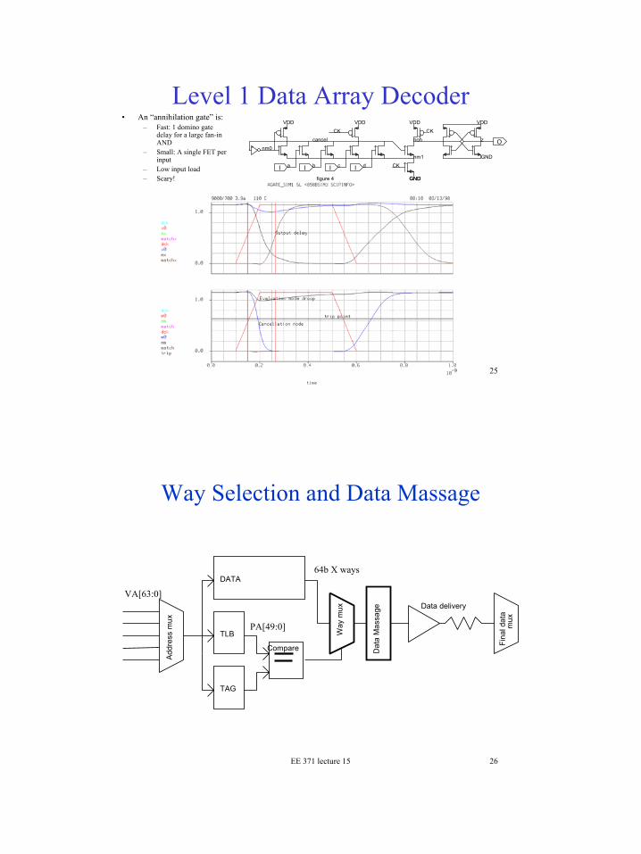
Level 1 Data Array Decoder• An “annihilation gate” is:
– Fast: 1 domino gate delay for a large fan-in AND
– Small: A single FET per input
– Low input load– Scary!
I
O
I II
CK
CK
nm0
VDD
GND
cancel
VDD
a b
z
c
figure 4
VDD
d
CK
GND
nm1
GND
VDD
noh
EE 371 lecture 15 26
Way Selection and Data Massage
Data delivery
Compare
DATA
TAG
TLB
Dat
a M
assa
ge
mux
Fina
l dat
a
Way
mux
Addr
ess
mux
VA[63:0]
PA[49:0]
64b X ways

14
EE 371 lecture 15 27
Rotating Way Mux• This block accomplishes 3 main tasks:
– Way Selection – Byte Rotation (for sub 8B loads)– Litte Endian / Big Endian Transformations
• A series of monotonicity-preserving static gates are used to perform the first stages of muxing.– Provides noise immunity– Allows phase stealing
• A pulse-precharged distributed pulldown network is used for the final stage.
O
I
I
I
rotation infoway selectdata
DataOutPCK
LogicStatic
EE 371 lecture 15 28
Rotating Way Mux
Way mux and store merge
select generators
I
I
I
I
I
I
I
I
I
I
O
II
I
I
OOI
I
I
O
both selects are active low
ZNN
_8
ZNN
_4
ZNN
_7
ZNN
_10
ZNN
_6
ZNN
_11
ZNN
_5
ZNN
_9
ZNN
_8
ZNN
_7
ZNN
_6
ZNN
_5ZN
N_4
ZNN
_3
ZNN
_1ZN
N_3
ZNN
_2
VDD
data
other input
VDD
leselhi
datahi
VDD
VDD
VDD
VDD
GND
VDD
leselhi
VDD
VDD
VDD
GND
VDD
GND
VDD VDD
GND
GND
dataout
lesello
besello
dataout
lesello
datalo
VDD
GND
VDD
GND
VDD
GNDGND
GND
beselhi
ldse
lhi
ldse
lhi
byps
ello
byps
elhi
nfor
ce0
stse
llo
ldse
llo
stse
lhi
ldse
llo
bypenhi
ldenloldenhi
bypenlo
stdathi
lddatlo
lddathi
stdatlo
waysel
(1)
(1)
(2)
(2.2)
(2)
(1)
(1)
(30)
(10)(10)
(3)
(3)
(1)(1)
(1)
(2)
(3)
(2.2)
(.8)
(1)
(1)
(1)(1)
(.8)
(2.2)
(3)
(.8)
(.8)
(.8)
(.8)
(2.2)
(3)
(.8)
(3)
(.8)
(1)
(3)
(2)
(2)
(1)
(1)
(1)
(2)
(3)(3)
(1)
(1)
(2)
(1)
(1)
(1)
•Painstaking Layout is critical•RC delay•Coupling•Size and features

15
EE 371 lecture 15 29
Finally: Delivering the Data• This requires careful wire engineering
– With all the parallelism in the execution unit, we had to use every last metal 4 track
– Since the cache data delivery is the latest arrival, we could demote a couple other tracks down to metal 2 to widen up the cache busses
• Almost a 50ps (5% of cycle) gainer
One bitslice in the address mux and output buffer circuit
Power
EE 371 lecture 15 30
Cache->Integer Bypass
sel_l1_0
sel_l1_1
sel_l1_1 sel_immsel_l1_0
L1D_1 IEU
sel_imm
L1D_0
NCK
IMM
sel_ieu
sel_ieu
NCK
result
NCK
pgate
npgate
High Strength Feedback for fast
rising edge
Mux selects enable pseudo-NMOS pullup
and latch reducing power and enabling stall
recovery
Enabled Latch
PullupPseudo-NMOS
pd
npgate
Noise problem?
Data delivery
Compare
DATA
TAG
TLB
Dat
a M
assa
ge
mux
Fina
l dat
a
Way
mux
Addr
ess
mux
16
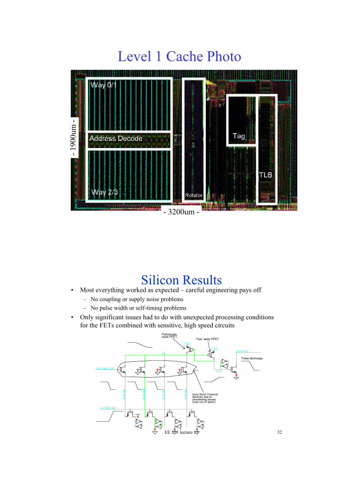
EE 371 lecture 15 31
Level 1 Cache Photo
- 3200um -
-190
0um
-
EE 371 lecture 15 32
Silicon Results• Most everything worked as expected – careful engineering pays off
– No coupling or supply noise problems– No pulse width or self-timing problems
• Only significant issues had to do with unexpected processing conditions for the FETs combined with sensitive, high speed circuits
weak PFETPathetically
Very Short Channel
False discharge
Fast, leaky PFET
(way out of spec!)processing issuesDevices due to
GNDGND
GND
VDD
GNDGND
GND
GND
p0
WORDLINE
VDDOUTPUT
VDD
noutCOLUMN_SEL
BITL
INE
BITL
INE
BITL
INE
BITL
INE

17
EE 371 lecture 15 33
Conclusions• There are plenty of opportunities to innovate in VLSI design
(and get paid for doing it!)– As long as silicon technology keeps advancing and changing, there
are new and interesting ways to exploit it– As long as information technology keeps driving our economy,
people will pay for performance and features• A few keys to finding the best way to contribute:
– Study the landscape; what’s been done before, the capabilities of the technology, what customers want
• Understand the architecture and performance issues, not just circuits– Pick one or two strategic areas to do something truly new (it will
always be more challenging than you thought)• For this example, we had the pre-validated tag, single-ended RAM and
annihilation gates, the rest was just tenacious engineering– Engineer the heck out of it; leave no stone unturned searching for
problems and applying airtight solutions
EE 371 lecture 15 34
Backup• Pulse
generator circuit
O
I
I
nout
nckd ckd
PCK
GND
VDDVDD
GND
SLCBO
GND
VDD
VDD
xpd
GND
VDD
VDD
GND
QUALH
GND
VDD
GND
VDD
FBN
VDD
xpu
PD
GND
qn1
VDD
NPU
(4)
(1)
(2.4)
(3.2)
(2)
(2)
(19.2)
(2.4)
(4)
(1)
(.28)
(.50)
(2)
(16)(63.6)
(.9/.3)
(.44)
(2.8/.24)
(4)
(6) (10)

18
EE 371 lecture 15 35
Backup: Coupling Noise Solutions
victim w/oantimiller
victim withantimiller
6ps extra delay
245mV less droop
• Top level cache read bitlines: 2mm, min space, precharged-pulldown, metal 4
• Anti-miller devices reduce crosstalk induced droops• Noise margins improved significantly with a small performance penalty
victim bitline
culprit bitline