ECEN689: Special Topics in High-Speed Links Circuits and...
22
Sam Palermo Analog & Mixed-Signal Center Texas A&M University ECEN689: Special Topics in High-Speed Links Circuits and Systems Spring 2010 Lecture 26: Phase-Locked Loops
Transcript of ECEN689: Special Topics in High-Speed Links Circuits and...

Sam PalermoAnalog & Mixed-Signal Center
Texas A&M University
ECEN689: Special Topics in High-Speed Links Circuits and Systems
Spring 2010
Lecture 26: Phase-Locked Loops
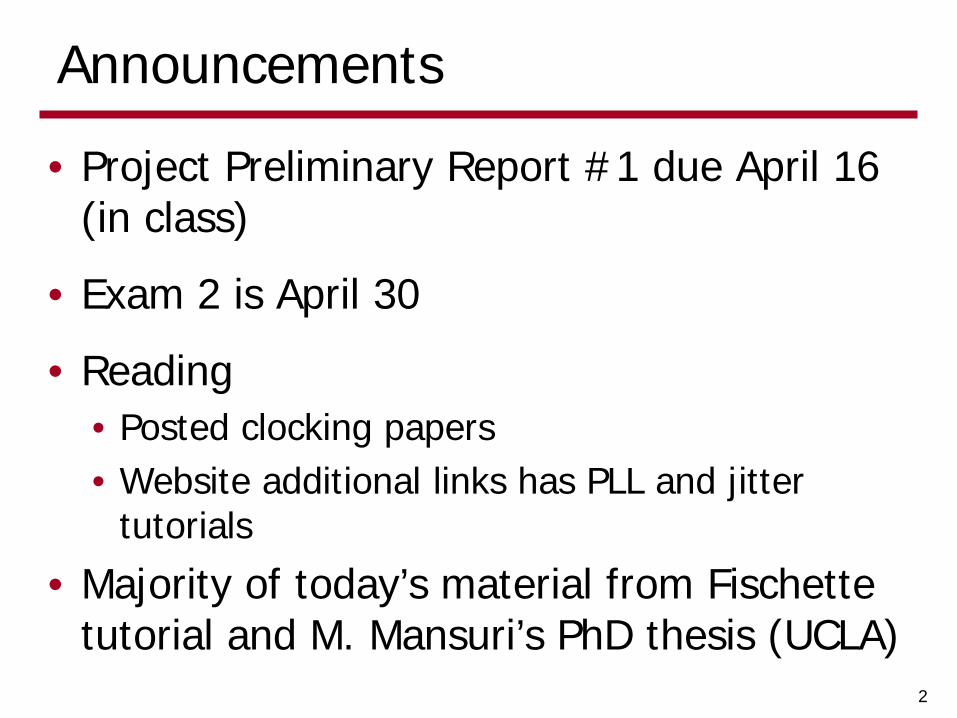
Announcements
• Project Preliminary Report #1 due April 16 (in class)
• Exam 2 is April 30
• Reading• Posted clocking papers• Website additional links has PLL and jitter
tutorials
• Majority of today’s material from Fischettetutorial and M. Mansuri’s PhD thesis (UCLA)
2
Agenda
• PLL modeling
3

Introduction
• A phase-locked loop (PLL) is a negative feedback system where an oscillator-generated signal is phase AND frequency locked to a reference signal
• PLLs applications• Frequency synthesis
• Multiplying a 100MHz reference clock to 10GHz
• Skew cancellation• Phase aligning an internal clock to an I/O clock
• Clock recovery• Extract from incoming data stream the clock frequency and optimum phase of
high-speed sampling clocks
• Modulation/De-modulation• Wireless systems• Spread-spectrum clocking
4

PLL Block Diagram
5
[Mansuri]
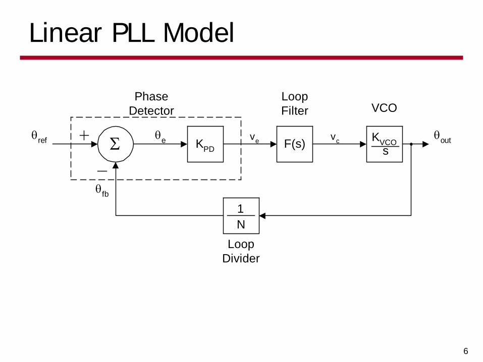
Linear PLL Model
6
Σθref θe veKPD
PhaseDetector
LoopFilter
vcF(s)
VCO
KVCOs
1N
θout
θfb
LoopDivider
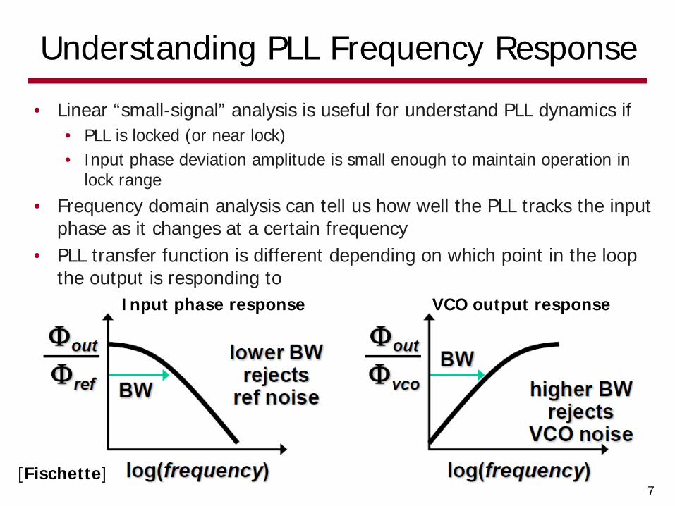
Understanding PLL Frequency Response
• Linear “small-signal” analysis is useful for understand PLL dynamics if• PLL is locked (or near lock)• Input phase deviation amplitude is small enough to maintain operation in
lock range
• Frequency domain analysis can tell us how well the PLL tracks the input phase as it changes at a certain frequency
• PLL transfer function is different depending on which point in the loop the output is responding to
7
Input phase response VCO output response
[Fischette]
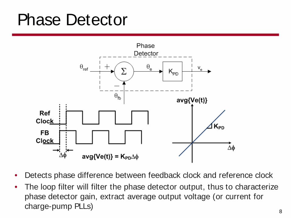
Phase Detector
• Detects phase difference between feedback clock and reference clock• The loop filter will filter the phase detector output, thus to characterize
phase detector gain, extract average output voltage (or current for charge-pump PLLs)
8
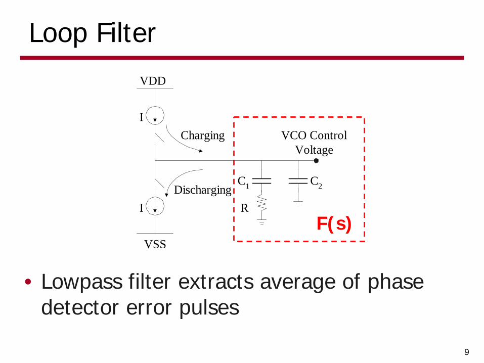
Loop Filter
• Lowpass filter extracts average of phase detector error pulses
9
I
I
VCO ControlVoltage
C1
R
C2
Charging
Discharging
VDD
VSSF(s)
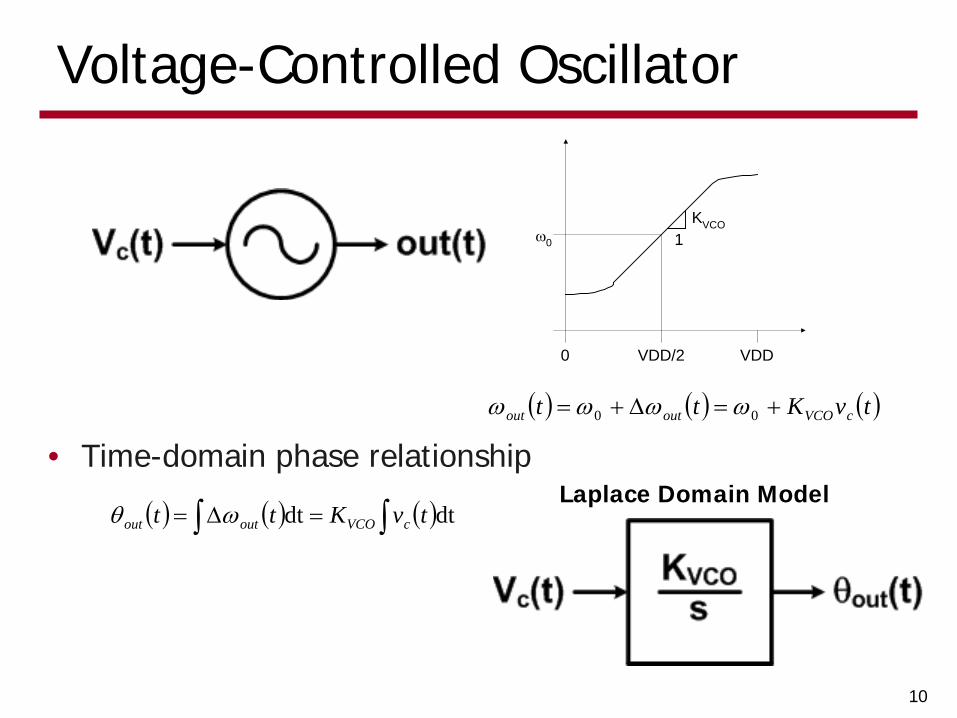
Voltage-Controlled Oscillator
• Time-domain phase relationship
10
VDDVDD/20
ω0 1KVCO
( ) ( ) ( )tvKtt cVCOoutout +=∆+= 00 ωωωω
( ) ( ) ( )∫ ∫=∆= dtdt tvKtt cVCOoutout ωθLaplace Domain Model

Loop Divider
• Time-domain model
11
( ) ( )tN
t outfb ωω 1=
( ) ( ) ( )∫ == tN
tN
t outoutfb θωθ 11 dt
[Perrott]

Linear PLL Model
12
Σθref θe veKPD
PhaseDetector
LoopFilter
vcF(s)
VCO
KVCOs
1N
θout
θfb
LoopDivider
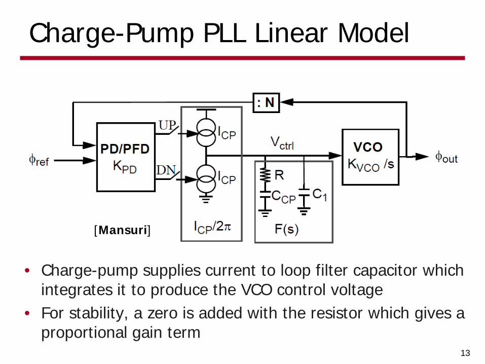
Charge-Pump PLL Linear Model
• Charge-pump supplies current to loop filter capacitor which integrates it to produce the VCO control voltage
• For stability, a zero is added with the resistor which gives a proportional gain term
13
[Mansuri]
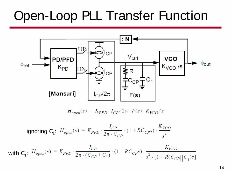
Open-Loop PLL Transfer Function
14
ignoring C1:
with C1:
[Mansuri]
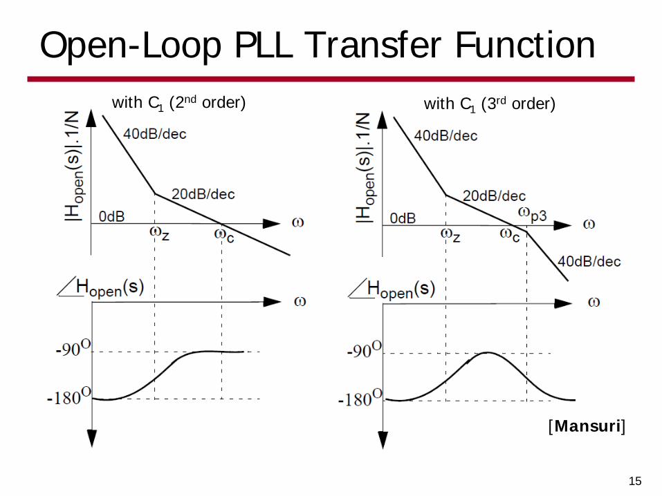
Open-Loop PLL Transfer Function
15
with C1 (3rd order)with C1 (2nd order)
[Mansuri]
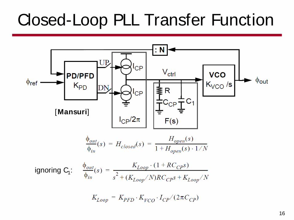
Closed-Loop PLL Transfer Function
16
ignoring C1:
[Mansuri]

PLL Natural Frequency and Damping Factor
17
22 2 nnss ωζω ++Standard 2nd-order denominator:
Damping Factor:
Natural Frequency:
( ) 21
23 1++= aandB ωω
−−+=
VCOPD
n
VCOPD
n
KKN
KKNa ω
ζω
ζ 412 2
Loop Bandwidth:
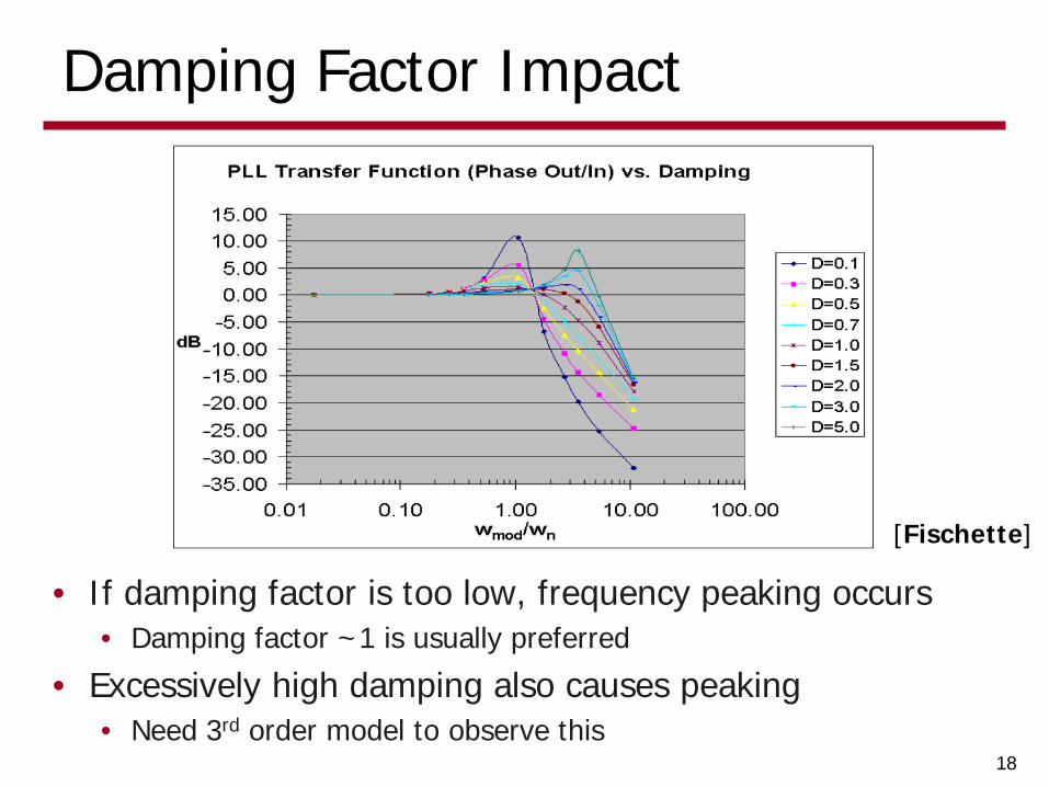
Damping Factor Impact
• If damping factor is too low, frequency peaking occurs• Damping factor ~1 is usually preferred
• Excessively high damping also causes peaking• Need 3rd order model to observe this
18
[Fischette]

Damping Factor Impact
• Peaking in frequency domain leads to ringing in the time domain
19
θref(s)=Frequency Step Input: ∆ωs2
KPD = 25uA/2πKVCO = 2π40MHz/V
N = 32ωn = 1 (normalized)
ζ = 0.1
ζ = 0.5
ζ = 0.707ζ = 1
ζ = 2

PLL Noise Transfer Function
20
[Mansuri]
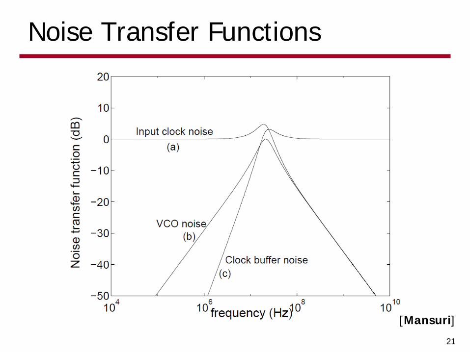
Noise Transfer Functions
21
[Mansuri]
Next Time
• PLL modeling• PLL circuits
22