
High speed CAN-AN - Infineon Technologies
68
High speed CAN Transceivers Application Note TLE6250G TLE6250GV33 TLE6251DS TLE6251G Author : Stéphane Fraissé Application Note, V1.0, Jan. 2006 Automotive Power
Transcript of High speed CAN-AN - Infineon Technologies

High speed CAN TransceiversAppl icat ion Note
TLE6250G
TLE6250GV33
TLE6251DS
TLE6251G
Author : Stéphane Fraissé
Appl icat ion Note, V1.0, Jan. 2006
Automot ive Power

Edition 2006-04-01Published by Infineon Technologies AG,St.-Martin-Strasse 53,81669 München, Germany© Infineon Technologies AG 2006.All Rights Reserved.
Attention please!The information given in this Data Sheet shall in no event be regarded as a guarantee of conditions or characteristics (“Beschaffenheitsgarantie”). With respect to any examples or hints given herein, any typical values stated herein and/or any information regarding the application of the device, Infineon Technologies hereby disclaims any and all warranties and liabilities of any kind, including without limitation warranties of non-infringement of intellectual property rights of any third party.
InformationFor further information on technology, delivery terms and conditions and prices please contact your nearest Infineon Technologies Office (www.infineon.com).
WarningsDue to technical requirements components may contain dangerous substances. For information on the types in question please contact your nearest Infineon Technologies Office.Infineon Technologies Components may only be used in life-support devices or systems with the express written approval of Infineon Technologies, if a failure of such components can reasonably be expected to cause the failure of that life-support device or system, or to affect the safety or effectiveness of that device or system. Life support devices or systems are intended to be implanted in the human body, or to support and/or maintain and sustain and/or protect human life. If they fail, it is reasonable to assume that the health of the user or other persons may be endangered.
Template: ap_a4_tmplt.fm / 2 / 2005-10-01
High speed CAN Revision History: 2006-04-01Previous Version: nonePage Subjects (major changes since last revision)

High speed CANCAN Transceiver
Application Note 4 V1.0, 2006-04-01

Application Note 1 V1.0, 2006-04-01
High speed CANCAN Transceiver
1 Introduction. . . . . . . . . . . . . . . . . . . . . . . . . . . . . . . . . . . . . . . . . . . . . . . . . . . . . . . . . . . . . . . . . . . . . 21.1 Recessive Level. . . . . . . . . . . . . . . . . . . . . . . . . . . . . . . . . . . . . . . . . . . . . . . . . . . . . . . . . . . . . . . . . . . 21.2 Dominant level. . . . . . . . . . . . . . . . . . . . . . . . . . . . . . . . . . . . . . . . . . . . . . . . . . . . . . . . . . . . . . . . . . . . 21.3 Driver symmetry. . . . . . . . . . . . . . . . . . . . . . . . . . . . . . . . . . . . . . . . . . . . . . . . . . . . . . . . . . . . . . . . . . . 3
2 In Vehicle Network. . . . . . . . . . . . . . . . . . . . . . . . . . . . . . . . . . . . . . . . . . . . . . . . . . . . . . . . . . . . . . . . 42.1 Type of supplies in the vehicle. . . . . . . . . . . . . . . . . . . . . . . . . . . . . . . . . . . . . . . . . . . . . . . . . . . . . . . . 42.1.1 Unsupplied modules in the parked car. (Clamp 15) . . . . . . . . . . . . . . . . . . . . . . . . . . . . . . . . . . . . . . 42.1.2 Supplied modules in the parked car. (Clamp 30) . . . . . . . . . . . . . . . . . . . . . . . . . . . . . . . . . . . . . . . . 42.1.3 Mixed network. . . . . . . . . . . . . . . . . . . . . . . . . . . . . . . . . . . . . . . . . . . . . . . . . . . . . . . . . . . . . . . . . . . 52.2 Ground line. . . . . . . . . . . . . . . . . . . . . . . . . . . . . . . . . . . . . . . . . . . . . . . . . . . . . . . . . . . . . . . . . . . . . . 52.2.1 High current applications. . . . . . . . . . . . . . . . . . . . . . . . . . . . . . . . . . . . . . . . . . . . . . . . . . . . . . . . . . 52.2.2 Low current application. . . . . . . . . . . . . . . . . . . . . . . . . . . . . . . . . . . . . . . . . . . . . . . . . . . . . . . . . . . . 62.3 The Transceiver in the automotive environment. . . . . . . . . . . . . . . . . . . . . . . . . . . . . . . . . . . . . . . . . . 62.3.1 Low battery voltage. . . . . . . . . . . . . . . . . . . . . . . . . . . . . . . . . . . . . . . . . . . . . . . . . . . . . . . . . . . . . . . 62.3.1.1 TLE6250G. . . . . . . . . . . . . . . . . . . . . . . . . . . . . . . . . . . . . . . . . . . . . . . . . . . . . . . . . . . . . . . . . . . 62.3.1.2 TLE6251DS. . . . . . . . . . . . . . . . . . . . . . . . . . . . . . . . . . . . . . . . . . . . . . . . . . . . . . . . . . . . . . . . . . 72.3.1.3 TLE6251G. . . . . . . . . . . . . . . . . . . . . . . . . . . . . . . . . . . . . . . . . . . . . . . . . . . . . . . . . . . . . . . . . . . 72.3.2 High battery voltage. . . . . . . . . . . . . . . . . . . . . . . . . . . . . . . . . . . . . . . . . . . . . . . . . . . . . . . . . . . . . . 72.3.2.1 TLE6250G / TLE6251DS. . . . . . . . . . . . . . . . . . . . . . . . . . . . . . . . . . . . . . . . . . . . . . . . . . . . . . . . 82.3.2.2 TLE6251G. . . . . . . . . . . . . . . . . . . . . . . . . . . . . . . . . . . . . . . . . . . . . . . . . . . . . . . . . . . . . . . . . . . 82.3.3 Reverse polarity. . . . . . . . . . . . . . . . . . . . . . . . . . . . . . . . . . . . . . . . . . . . . . . . . . . . . . . . . . . . . . . . . 82.3.3.1 TLE6250G / TLE6251DS. . . . . . . . . . . . . . . . . . . . . . . . . . . . . . . . . . . . . . . . . . . . . . . . . . . . . . . . 82.3.3.2 TLE6251G. . . . . . . . . . . . . . . . . . . . . . . . . . . . . . . . . . . . . . . . . . . . . . . . . . . . . . . . . . . . . . . . . . . 82.3.4 Short circuit on the bus. . . . . . . . . . . . . . . . . . . . . . . . . . . . . . . . . . . . . . . . . . . . . . . . . . . . . . . . . . . . 82.3.4.1 Termination resistors case in short circuit to Vbat. . . . . . . . . . . . . . . . . . . . . . . . . . . . . . . . . . . . . 82.3.5 Temperature. . . . . . . . . . . . . . . . . . . . . . . . . . . . . . . . . . . . . . . . . . . . . . . . . . . . . . . . . . . . . . . . . . . . 92.3.6 Ground shift. . . . . . . . . . . . . . . . . . . . . . . . . . . . . . . . . . . . . . . . . . . . . . . . . . . . . . . . . . . . . . . . . . . . 92.3.7 Loss of ground. . . . . . . . . . . . . . . . . . . . . . . . . . . . . . . . . . . . . . . . . . . . . . . . . . . . . . . . . . . . . . . . . 112.3.8 Loss of Battery. . . . . . . . . . . . . . . . . . . . . . . . . . . . . . . . . . . . . . . . . . . . . . . . . . . . . . . . . . . . . . . . . 12
3 Power management, transceiver supply. . . . . . . . . . . . . . . . . . . . . . . . . . . . . . . . . . . . . . . . . . . . . 133.1 TLE6250G. . . . . . . . . . . . . . . . . . . . . . . . . . . . . . . . . . . . . . . . . . . . . . . . . . . . . . . . . . . . . . . . . . . . . . 133.1.1 TLE6250G in unsupplied mode. . . . . . . . . . . . . . . . . . . . . . . . . . . . . . . . . . . . . . . . . . . . . . . . . . . . 133.1.2 TLE6250G in inhibit mode. . . . . . . . . . . . . . . . . . . . . . . . . . . . . . . . . . . . . . . . . . . . . . . . . . . . . . . . 133.1.3 TLE6250G in normal mode. . . . . . . . . . . . . . . . . . . . . . . . . . . . . . . . . . . . . . . . . . . . . . . . . . . . . . . . 133.1.4 TLE6250G in fault condition. . . . . . . . . . . . . . . . . . . . . . . . . . . . . . . . . . . . . . . . . . . . . . . . . . . . . . . 133.1.4.1 Average maximum current in fault condition. . . . . . . . . . . . . . . . . . . . . . . . . . . . . . . . . . . . . . . . . 133.1.4.2 Peak maximum current and decoupling capacitor. . . . . . . . . . . . . . . . . . . . . . . . . . . . . . . . . . . . 133.1.5 TLE6250G junction temperature. . . . . . . . . . . . . . . . . . . . . . . . . . . . . . . . . . . . . . . . . . . . . . . . . . . . 143.2 TLE6251DS. . . . . . . . . . . . . . . . . . . . . . . . . . . . . . . . . . . . . . . . . . . . . . . . . . . . . . . . . . . . . . . . . . . . . 143.2.1 TLE6251DS in unsupplied mode. . . . . . . . . . . . . . . . . . . . . . . . . . . . . . . . . . . . . . . . . . . . . . . . . . . 143.2.2 TLE6251DS in stand by mode. . . . . . . . . . . . . . . . . . . . . . . . . . . . . . . . . . . . . . . . . . . . . . . . . . . . . 153.2.3 TLE6251DS in normal mode. . . . . . . . . . . . . . . . . . . . . . . . . . . . . . . . . . . . . . . . . . . . . . . . . . . . . . 153.2.4 TLE6251DS in fault condition. . . . . . . . . . . . . . . . . . . . . . . . . . . . . . . . . . . . . . . . . . . . . . . . . . . . . . 153.2.5 TLE6251DS junction temperature. . . . . . . . . . . . . . . . . . . . . . . . . . . . . . . . . . . . . . . . . . . . . . . . . . 153.3 TLE6251G. . . . . . . . . . . . . . . . . . . . . . . . . . . . . . . . . . . . . . . . . . . . . . . . . . . . . . . . . . . . . . . . . . . . . . 153.3.1 TLE6251G in unsupplied mode. . . . . . . . . . . . . . . . . . . . . . . . . . . . . . . . . . . . . . . . . . . . . . . . . . . . 163.3.2 TLE6251G in sleep mode. . . . . . . . . . . . . . . . . . . . . . . . . . . . . . . . . . . . . . . . . . . . . . . . . . . . . . . . . 163.3.3 TLE6251G in Stand by mode. . . . . . . . . . . . . . . . . . . . . . . . . . . . . . . . . . . . . . . . . . . . . . . . . . . . . . 163.3.4 TLE6251G in receive only mode. . . . . . . . . . . . . . . . . . . . . . . . . . . . . . . . . . . . . . . . . . . . . . . . . . . 173.3.5 TLE6251G in normal mode. . . . . . . . . . . . . . . . . . . . . . . . . . . . . . . . . . . . . . . . . . . . . . . . . . . . . . . . 17

High speed CANCAN Transceiver
Application Note 2 V1.0, 2006-04-01
3.3.6 TLE6251G in fault condition. . . . . . . . . . . . . . . . . . . . . . . . . . . . . . . . . . . . . . . . . . . . . . . . . . . . . . . 173.3.7 TLE6251G junction temperature. . . . . . . . . . . . . . . . . . . . . . . . . . . . . . . . . . . . . . . . . . . . . . . . . . . . 173.3.8 Choice of the voltage regulator. . . . . . . . . . . . . . . . . . . . . . . . . . . . . . . . . . . . . . . . . . . . . . . . . . . . . 17
4 Interface with micro controller. . . . . . . . . . . . . . . . . . . . . . . . . . . . . . . . . . . . . . . . . . . . . . . . . . . . . 184.1 TLE6250G/GV33. . . . . . . . . . . . . . . . . . . . . . . . . . . . . . . . . . . . . . . . . . . . . . . . . . . . . . . . . . . . . . . . . 184.1.1 Pin Vcc . . . . . . . . . . . . . . . . . . . . . . . . . . . . . . . . . . . . . . . . . . . . . . . . . . . . . . . . . . . . . . . . . . . . . . . 184.1.2 Pin RM (only for the TLE6250G version). . . . . . . . . . . . . . . . . . . . . . . . . . . . . . . . . . . . . . . . . . . . . 194.1.3 Pin INH. . . . . . . . . . . . . . . . . . . . . . . . . . . . . . . . . . . . . . . . . . . . . . . . . . . . . . . . . . . . . . . . . . . . . . . 194.1.4 Pin V33 or Vio (only for TLE6250GV33). . . . . . . . . . . . . . . . . . . . . . . . . . . . . . . . . . . . . . . . . . . . . . 194.1.5 Pin TxD. . . . . . . . . . . . . . . . . . . . . . . . . . . . . . . . . . . . . . . . . . . . . . . . . . . . . . . . . . . . . . . . . . . . . . . 204.1.6 Pin RxD. . . . . . . . . . . . . . . . . . . . . . . . . . . . . . . . . . . . . . . . . . . . . . . . . . . . . . . . . . . . . . . . . . . . . . . 204.2 TLE6251DS. . . . . . . . . . . . . . . . . . . . . . . . . . . . . . . . . . . . . . . . . . . . . . . . . . . . . . . . . . . . . . . . . . . . . 224.2.1 Pin STB. . . . . . . . . . . . . . . . . . . . . . . . . . . . . . . . . . . . . . . . . . . . . . . . . . . . . . . . . . . . . . . . . . . . . . . 224.2.2 Pin TxD. . . . . . . . . . . . . . . . . . . . . . . . . . . . . . . . . . . . . . . . . . . . . . . . . . . . . . . . . . . . . . . . . . . . . . . 224.2.2.1 Hardware description. . . . . . . . . . . . . . . . . . . . . . . . . . . . . . . . . . . . . . . . . . . . . . . . . . . . . . . . . . 224.2.2.2 Time out function. . . . . . . . . . . . . . . . . . . . . . . . . . . . . . . . . . . . . . . . . . . . . . . . . . . . . . . . . . . . . 224.2.2.3 Time out function. Baud rate limitation. . . . . . . . . . . . . . . . . . . . . . . . . . . . . . . . . . . . . . . . . . . . . 234.2.3 Pin RxD. . . . . . . . . . . . . . . . . . . . . . . . . . . . . . . . . . . . . . . . . . . . . . . . . . . . . . . . . . . . . . . . . . . . . . . 234.2.3.1 Hardware description. . . . . . . . . . . . . . . . . . . . . . . . . . . . . . . . . . . . . . . . . . . . . . . . . . . . . . . . . . 234.2.3.2 Wake up behavior. . . . . . . . . . . . . . . . . . . . . . . . . . . . . . . . . . . . . . . . . . . . . . . . . . . . . . . . . . . . . 234.2.3.3 Delay from stand by to normal mode. . . . . . . . . . . . . . . . . . . . . . . . . . . . . . . . . . . . . . . . . . . . . . 244.3 TLE6251G. . . . . . . . . . . . . . . . . . . . . . . . . . . . . . . . . . . . . . . . . . . . . . . . . . . . . . . . . . . . . . . . . . . . . . 254.3.1 Pin TxD. . . . . . . . . . . . . . . . . . . . . . . . . . . . . . . . . . . . . . . . . . . . . . . . . . . . . . . . . . . . . . . . . . . . . . . 254.3.2 Pin RxD. . . . . . . . . . . . . . . . . . . . . . . . . . . . . . . . . . . . . . . . . . . . . . . . . . . . . . . . . . . . . . . . . . . . . . . 254.3.3 Pin EN. . . . . . . . . . . . . . . . . . . . . . . . . . . . . . . . . . . . . . . . . . . . . . . . . . . . . . . . . . . . . . . . . . . . . . . . 254.3.4 Pin NSTB. . . . . . . . . . . . . . . . . . . . . . . . . . . . . . . . . . . . . . . . . . . . . . . . . . . . . . . . . . . . . . . . . . . . . 254.3.5 Pin VµC. . . . . . . . . . . . . . . . . . . . . . . . . . . . . . . . . . . . . . . . . . . . . . . . . . . . . . . . . . . . . . . . . . . . . . . 264.3.5.1 VµC pin´s maximum current. . . . . . . . . . . . . . . . . . . . . . . . . . . . . . . . . . . . . . . . . . . . . . . . . . . . . 264.3.5.2 Vµc under voltage detection. . . . . . . . . . . . . . . . . . . . . . . . . . . . . . . . . . . . . . . . . . . . . . . . . . . . . 264.3.6 pin Vcc. . . . . . . . . . . . . . . . . . . . . . . . . . . . . . . . . . . . . . . . . . . . . . . . . . . . . . . . . . . . . . . . . . . . . . . 274.3.7 Pin NERR. . . . . . . . . . . . . . . . . . . . . . . . . . . . . . . . . . . . . . . . . . . . . . . . . . . . . . . . . . . . . . . . . . . . . 274.3.7.1 Possible bus errors cases. . . . . . . . . . . . . . . . . . . . . . . . . . . . . . . . . . . . . . . . . . . . . . . . . . . . . . . 274.3.7.2 Pin NERR in short circuit. . . . . . . . . . . . . . . . . . . . . . . . . . . . . . . . . . . . . . . . . . . . . . . . . . . . . . . 274.3.8 Pin INH. . . . . . . . . . . . . . . . . . . . . . . . . . . . . . . . . . . . . . . . . . . . . . . . . . . . . . . . . . . . . . . . . . . . . . . 274.3.8.1 Pin INH purpose. . . . . . . . . . . . . . . . . . . . . . . . . . . . . . . . . . . . . . . . . . . . . . . . . . . . . . . . . . . . . . 274.3.8.2 Pin INH power capability. . . . . . . . . . . . . . . . . . . . . . . . . . . . . . . . . . . . . . . . . . . . . . . . . . . . . . . . 284.3.8.3 Pin INH driving the INH input of an Voltage regulator. . . . . . . . . . . . . . . . . . . . . . . . . . . . . . . . . 284.3.8.4 Wake up timing with pin INH. . . . . . . . . . . . . . . . . . . . . . . . . . . . . . . . . . . . . . . . . . . . . . . . . . . . . 284.3.9 pin WK. . . . . . . . . . . . . . . . . . . . . . . . . . . . . . . . . . . . . . . . . . . . . . . . . . . . . . . . . . . . . . . . . . . . . . . 294.3.10 Software issues consideration for TLE6251G. . . . . . . . . . . . . . . . . . . . . . . . . . . . . . . . . . . . . . . . . 324.3.10.1 Cold start. . . . . . . . . . . . . . . . . . . . . . . . . . . . . . . . . . . . . . . . . . . . . . . . . . . . . . . . . . . . . . . . . . . 324.3.10.2 Hot start. . . . . . . . . . . . . . . . . . . . . . . . . . . . . . . . . . . . . . . . . . . . . . . . . . . . . . . . . . . . . . . . . . . . 324.3.10.3 Enter the Standby mode. . . . . . . . . . . . . . . . . . . . . . . . . . . . . . . . . . . . . . . . . . . . . . . . . . . . . . . . 324.3.10.4 Enter the Sleep mode. . . . . . . . . . . . . . . . . . . . . . . . . . . . . . . . . . . . . . . . . . . . . . . . . . . . . . . . . . 33
5 Bus pins. Terminations concepts. . . . . . . . . . . . . . . . . . . . . . . . . . . . . . . . . . . . . . . . . . . . . . . . . . 375.1 Termination resistors. . . . . . . . . . . . . . . . . . . . . . . . . . . . . . . . . . . . . . . . . . . . . . . . . . . . . . . . . . . . . . 375.2 Split pin. . . . . . . . . . . . . . . . . . . . . . . . . . . . . . . . . . . . . . . . . . . . . . . . . . . . . . . . . . . . . . . . . . . . . . . . 375.2.1 Recessive voltage in a mixed Clamp 15 / 30 network, without SPLIT. . . . . . . . . . . . . . . . . . . . . . . 375.2.2 Recessive voltage in a mixed Clamp 15 / 30 network, with SPLIT. . . . . . . . . . . . . . . . . . . . . . . . . . 385.3 CAN_H / CAN_L. . . . . . . . . . . . . . . . . . . . . . . . . . . . . . . . . . . . . . . . . . . . . . . . . . . . . . . . . . . . . . . . . 40

Application Note 3 V1.0, 2006-04-01
High speed CANCAN Transceiver
6 ESD Aspects. . . . . . . . . . . . . . . . . . . . . . . . . . . . . . . . . . . . . . . . . . . . . . . . . . . . . . . . . . . . . . . . . . . 416.1 ESD tests definition. . . . . . . . . . . . . . . . . . . . . . . . . . . . . . . . . . . . . . . . . . . . . . . . . . . . . . . . . . . . . . . 416.1.1 Human Body Model test. (MIL-STD 883). . . . . . . . . . . . . . . . . . . . . . . . . . . . . . . . . . . . . . . . . . . . . 416.1.2 Gun test. (IEC 61000-4-2). . . . . . . . . . . . . . . . . . . . . . . . . . . . . . . . . . . . . . . . . . . . . . . . . . . . . . . . 416.1.3 Charged Device Model (CDM). . . . . . . . . . . . . . . . . . . . . . . . . . . . . . . . . . . . . . . . . . . . . . . . . . . . . 426.1.4 Machine Model (MM). . . . . . . . . . . . . . . . . . . . . . . . . . . . . . . . . . . . . . . . . . . . . . . . . . . . . . . . . . . . 436.2 ESD protection. . . . . . . . . . . . . . . . . . . . . . . . . . . . . . . . . . . . . . . . . . . . . . . . . . . . . . . . . . . . . . . . . . . 436.3 Modules under ESD gun test. . . . . . . . . . . . . . . . . . . . . . . . . . . . . . . . . . . . . . . . . . . . . . . . . . . . . . . . 436.3.1 Device without any external protection circuitry. . . . . . . . . . . . . . . . . . . . . . . . . . . . . . . . . . . . . . . . 446.3.2 ESD level reached with a choke coil. . . . . . . . . . . . . . . . . . . . . . . . . . . . . . . . . . . . . . . . . . . . . . . . . 456.3.3 ESD level reached with a choke coil and ESD diode or varistor. . . . . . . . . . . . . . . . . . . . . . . . . . . 456.4 PCB layout. . . . . . . . . . . . . . . . . . . . . . . . . . . . . . . . . . . . . . . . . . . . . . . . . . . . . . . . . . . . . . . . . . . . . . 476.5 Conclusion. . . . . . . . . . . . . . . . . . . . . . . . . . . . . . . . . . . . . . . . . . . . . . . . . . . . . . . . . . . . . . . . . . . . . . 47
7 EMC aspect. . . . . . . . . . . . . . . . . . . . . . . . . . . . . . . . . . . . . . . . . . . . . . . . . . . . . . . . . . . . . . . . . . . . 497.1 EM Immunity against transcients. . . . . . . . . . . . . . . . . . . . . . . . . . . . . . . . . . . . . . . . . . . . . . . . . . . . . 497.2 EM Immunity against RF disturbances. . . . . . . . . . . . . . . . . . . . . . . . . . . . . . . . . . . . . . . . . . . . . . . . 497.2.1 The Stripline test. ISO 11452-5. . . . . . . . . . . . . . . . . . . . . . . . . . . . . . . . . . . . . . . . . . . . . . . . . . . . 497.2.2 The Bulk Current Injection test. (BCI). ISO 11452-4. . . . . . . . . . . . . . . . . . . . . . . . . . . . . . . . . . . . . 497.3 Infineon transceivers in the EMI disturbances. . . . . . . . . . . . . . . . . . . . . . . . . . . . . . . . . . . . . . . . . . . 497.3.1 Immunity against transcients. . . . . . . . . . . . . . . . . . . . . . . . . . . . . . . . . . . . . . . . . . . . . . . . . . . . . . 497.3.1.1 Damage test. . . . . . . . . . . . . . . . . . . . . . . . . . . . . . . . . . . . . . . . . . . . . . . . . . . . . . . . . . . . . . . . . 497.3.1.2 Malfunction test. . . . . . . . . . . . . . . . . . . . . . . . . . . . . . . . . . . . . . . . . . . . . . . . . . . . . . . . . . . . . . . 507.3.2 Immunity against RF disturbances. . . . . . . . . . . . . . . . . . . . . . . . . . . . . . . . . . . . . . . . . . . . . . . . . . 507.3.2.1 BCI test limitation . . . . . . . . . . . . . . . . . . . . . . . . . . . . . . . . . . . . . . . . . . . . . . . . . . . . . . . . . . . . . 507.3.2.2 Principle of the DPI test. . . . . . . . . . . . . . . . . . . . . . . . . . . . . . . . . . . . . . . . . . . . . . . . . . . . . . . . 507.3.2.3 Results of Infineon’s transceiver under DPI test. . . . . . . . . . . . . . . . . . . . . . . . . . . . . . . . . . . . . . 517.3.2.4 Improvement of the DPI result. Use of choke coil. . . . . . . . . . . . . . . . . . . . . . . . . . . . . . . . . . . . 527.3.3 Emission . . . . . . . . . . . . . . . . . . . . . . . . . . . . . . . . . . . . . . . . . . . . . . . . . . . . . . . . . . . . . . . . . . . . . 537.4 Conclusion. . . . . . . . . . . . . . . . . . . . . . . . . . . . . . . . . . . . . . . . . . . . . . . . . . . . . . . . . . . . . . . . . . . . . . 55
8 Products summary . . . . . . . . . . . . . . . . . . . . . . . . . . . . . . . . . . . . . . . . . . . . . . . . . . . . . . . . . . . . . . 56
9 References. . . . . . . . . . . . . . . . . . . . . . . . . . . . . . . . . . . . . . . . . . . . . . . . . . . . . . . . . . . . . . . . . . . . . 57

High speed CANCAN Transceiver
Application Note 4 V1.0, 2006-04-01

Application Note 1 V1.0, 2006-04-01
High speed CANCAN Transceiver
Figure 1 Typical high speed CAN signal. . . . . . . . . . . . . . . . . . . . . . . . . . . . . . . . . . . . . . . . . . . . . . . . . . . . . 2Figure 2 Dominant level . . . . . . . . . . . . . . . . . . . . . . . . . . . . . . . . . . . . . . . . . . . . . . . . . . . . . . . . . . . . . . . . . 3Figure 3 Common mode voltage definition. . . . . . . . . . . . . . . . . . . . . . . . . . . . . . . . . . . . . . . . . . . . . . . . . . . 3Figure 4 Typical Clamp 15 application . . . . . . . . . . . . . . . . . . . . . . . . . . . . . . . . . . . . . . . . . . . . . . . . . . . . . . 4Figure 5 Typical Clamp 30 application . . . . . . . . . . . . . . . . . . . . . . . . . . . . . . . . . . . . . . . . . . . . . . . . . . . . . . 4Figure 6 Mixed CL15 and CL30 network . . . . . . . . . . . . . . . . . . . . . . . . . . . . . . . . . . . . . . . . . . . . . . . . . . . . 5Figure 7 Typical high current application . . . . . . . . . . . . . . . . . . . . . . . . . . . . . . . . . . . . . . . . . . . . . . . . . . . . 6Figure 8 Undervoltage detection mechanism for Vs. . . . . . . . . . . . . . . . . . . . . . . . . . . . . . . . . . . . . . . . . . . . 7Figure 9 Current in the termination resistors in case of short circuit to Vbat. . . . . . . . . . . . . . . . . . . . . . . . . . 9Figure 10 System with one ground shift event . . . . . . . . . . . . . . . . . . . . . . . . . . . . . . . . . . . . . . . . . . . . . . . . . 9Figure 11 Typical DC ground shift signal. . . . . . . . . . . . . . . . . . . . . . . . . . . . . . . . . . . . . . . . . . . . . . . . . . . . . 10Figure 12 CAN signals with AC ground shift. . . . . . . . . . . . . . . . . . . . . . . . . . . . . . . . . . . . . . . . . . . . . . . . . . 11Figure 13 Loss of ground with inductive load . . . . . . . . . . . . . . . . . . . . . . . . . . . . . . . . . . . . . . . . . . . . . . . . . 12Figure 14 Buffer capacitor in function of the baud rate. . . . . . . . . . . . . . . . . . . . . . . . . . . . . . . . . . . . . . . . . . 14Figure 15 Quiescent current computation in stand by mode. . . . . . . . . . . . . . . . . . . . . . . . . . . . . . . . . . . . . . 15Figure 16 Quiescent current computation in sleep mode, with and without inhibit functionnality. . . . . . . . . . 16Figure 17 Block diagram of TLE6250G/ TLE6250GV33. . . . . . . . . . . . . . . . . . . . . . . . . . . . . . . . . . . . . . . . . 18Figure 18 Module connection verification, using receive only mode functionnality. . . . . . . . . . . . . . . . . . . . . 19Figure 19 parasitic delay in case of serial resistor. . . . . . . . . . . . . . . . . . . . . . . . . . . . . . . . . . . . . . . . . . . . . . 20Figure 20 receiver timing . . . . . . . . . . . . . . . . . . . . . . . . . . . . . . . . . . . . . . . . . . . . . . . . . . . . . . . . . . . . . . . . 20Figure 21 Typical application for TLE6250G. . . . . . . . . . . . . . . . . . . . . . . . . . . . . . . . . . . . . . . . . . . . . . . . . . 21Figure 22 Typical application for TLE6250GV33. . . . . . . . . . . . . . . . . . . . . . . . . . . . . . . . . . . . . . . . . . . . . . . 21Figure 23 Pin out comparison TLE6251DS and TLE6250G. . . . . . . . . . . . . . . . . . . . . . . . . . . . . . . . . . . . . . 22Figure 24 Permanent dominant time out feature. . . . . . . . . . . . . . . . . . . . . . . . . . . . . . . . . . . . . . . . . . . . . . . 22Figure 25 Wake up timing. . . . . . . . . . . . . . . . . . . . . . . . . . . . . . . . . . . . . . . . . . . . . . . . . . . . . . . . . . . . . . . . 23Figure 26 Delay from stand by to normal mode timing. . . . . . . . . . . . . . . . . . . . . . . . . . . . . . . . . . . . . . . . . . 24Figure 27 Typical application for the TLE6251DS. . . . . . . . . . . . . . . . . . . . . . . . . . . . . . . . . . . . . . . . . . . . . . 24Figure 28 Pin out comparison TLE6251DS and TLE6251G. . . . . . . . . . . . . . . . . . . . . . . . . . . . . . . . . . . . . . 25Figure 29 TLE6251G Mode state diagram . . . . . . . . . . . . . . . . . . . . . . . . . . . . . . . . . . . . . . . . . . . . . . . . . . . 26Figure 30 Possible failure cases failures on the bus word list. (According ISO 11898) . . . . . . . . . . . . . . . . . 27Figure 31 Circuitry for the INH output . . . . . . . . . . . . . . . . . . . . . . . . . . . . . . . . . . . . . . . . . . . . . . . . . . . . . . . 28Figure 32 Possible wake up circuitries.. . . . . . . . . . . . . . . . . . . . . . . . . . . . . . . . . . . . . . . . . . . . . . . . . . . . . . 29Figure 33 Wake up timing with INH function. Cold start. . . . . . . . . . . . . . . . . . . . . . . . . . . . . . . . . . . . . . . . . 30Figure 34 Typical application circuit for TLE6251G, with separate 3.3V VµC and 5V Vcc supply . . . . . . . . . 31Figure 35 Flow diagram for an ECU cold start.. . . . . . . . . . . . . . . . . . . . . . . . . . . . . . . . . . . . . . . . . . . . . . . . 34Figure 36 Flow diagram for an ECU warm start.. . . . . . . . . . . . . . . . . . . . . . . . . . . . . . . . . . . . . . . . . . . . . . . 35Figure 37 Flow diagram to enter Stand by mode . . . . . . . . . . . . . . . . . . . . . . . . . . . . . . . . . . . . . . . . . . . . . . 35Figure 38 Flow diagram to enter Sleep mode. . . . . . . . . . . . . . . . . . . . . . . . . . . . . . . . . . . . . . . . . . . . . . . . . 36Figure 39 Application circuitry for the split pin. . . . . . . . . . . . . . . . . . . . . . . . . . . . . . . . . . . . . . . . . . . . . . . . . 37Figure 40 Equivalent electrical schematic for a mixed network without split pin. . . . . . . . . . . . . . . . . . . . . . . 38Figure 41 Equivalent electrical schematic for a mixed network with SPLIT pin . . . . . . . . . . . . . . . . . . . . . . . 38Figure 42 Recessive level for different configurations in a mixed network with split. . . . . . . . . . . . . . . . . . . . 39Figure 43 Current flowing in the TLE6250G ground, function of the ESD voltage. Device unsupplied . . . . . 41Figure 44 Comparison of the current between HBM and gun test.. . . . . . . . . . . . . . . . . . . . . . . . . . . . . . . . . 42Figure 45 ESD test equipement . . . . . . . . . . . . . . . . . . . . . . . . . . . . . . . . . . . . . . . . . . . . . . . . . . . . . . . . . . . 42Figure 46 Standard and Infineon ESD protection . . . . . . . . . . . . . . . . . . . . . . . . . . . . . . . . . . . . . . . . . . . . . . 43Figure 47 Schematic of the test . . . . . . . . . . . . . . . . . . . . . . . . . . . . . . . . . . . . . . . . . . . . . . . . . . . . . . . . . . . 44Figure 48 Positive ESD discharge, device supplied. Read out of the ground and supply current. . . . . . . . . . 44Figure 49 Negative ESD discharge, device supplied. Read out of the ground and supply current. . . . . . . . . 45Figure 50 ESD discharge, device supplied. Read out of the ground current. With choke coil.. . . . . . . . . . . . 45Figure 51 Positive ESD discharge, device supplied. Read out of the ground current. With varistor. . . . . . . . 46

High speed CANCAN Transceiver
Application Note 2 V1.0, 2006-04-01
Figure 52 Negative ESD discharge, device supplied. Read out of the ground current. With varistor. . . . . . . 46Figure 53 Bad PCB example for ESD. . . . . . . . . . . . . . . . . . . . . . . . . . . . . . . . . . . . . . . . . . . . . . . . . . . . . . . 47Figure 54 Good PCB design for ESD robustness. . . . . . . . . . . . . . . . . . . . . . . . . . . . . . . . . . . . . . . . . . . . . . 48Figure 55 BCI test limitation example . . . . . . . . . . . . . . . . . . . . . . . . . . . . . . . . . . . . . . . . . . . . . . . . . . . . . . . 50Figure 56 DPI test set up . . . . . . . . . . . . . . . . . . . . . . . . . . . . . . . . . . . . . . . . . . . . . . . . . . . . . . . . . . . . . . . . 51Figure 57 DPI test results example : The TLE6250G . . . . . . . . . . . . . . . . . . . . . . . . . . . . . . . . . . . . . . . . . . . 52Figure 58 Choke coil principle. . . . . . . . . . . . . . . . . . . . . . . . . . . . . . . . . . . . . . . . . . . . . . . . . . . . . . . . . . . . . 53Figure 59 DPI test results with choke coil for the TLE6250G. . . . . . . . . . . . . . . . . . . . . . . . . . . . . . . . . . . . . 53Figure 60 EME test results with TLE6250G, without chock coil . . . . . . . . . . . . . . . . . . . . . . . . . . . . . . . . . . . 54Figure 61 EME test results with TLE6250G with and without chock coil . . . . . . . . . . . . . . . . . . . . . . . . . . . . 54

Application Note 1 V1.0, 2006-04-01
High speed CANCAN Transceiver
Table 1 DC parameters for recessive output of CAN node . . . . . . . . . . . . . . . . . . . . . . . . . . . . . . . . . . . . . . 2Table 2 DC parameters for dominant output of CAN node . . . . . . . . . . . . . . . . . . . . . . . . . . . . . . . . . . . . . . 3Table 3 Driver symmetry . . . . . . . . . . . . . . . . . . . . . . . . . . . . . . . . . . . . . . . . . . . . . . . . . . . . . . . . . . . . . . . . 3Table 4 Damage test . . . . . . . . . . . . . . . . . . . . . . . . . . . . . . . . . . . . . . . . . . . . . . . . . . . . . . . . . . . . . . . . . . 49

High speed CANCAN Transceiver
Introduction. Recessive Level.
Application Note 2 V1.0, 2006-04-01
1 Introduction.The increasing number of electronics equipment in todays cars implies a lot of information exchange. To avoid amassive usage of wires between modules, a digital protocol has been created. This protocol has been named CANfor Controller Area Network. CAN allows communication, to a speed up to 1Mbit/s. To avoid noisy communicationin terms of electromagnetic emission, the medium is a twisted pair and the electrical signal is differential. Figure 1shows the typical signal of high speed CAN, and the basic reason for low electro-magnetic emission. WhenCAN_H rises, some parasitic are emitted. In the same time, CAN_L goes down, in the same proportion. The sumof these parasitics are 0, so to say the electromagnetic emission is limited.
Figure 1 Typical high speed CAN signal
This application note is intended to present the high speed CAN application and the usage of Infineon CANtransceivers in these applications. This document refers to international standard ISO 11898-2 [5], SAE J2284,ISO 11898-5 [6], and well as to the TLE6250G [1],TLE6251DS [2], and TLE6251G [3] datasheets. First part of the document will describes high speed CAN network in the automotive environnement. Then it willfocus on transceivers itself for easy interfacing with micro-controller, and will conclude by application hints tosuccessfully reach the challenges of such networks require.
1.1 Recessive Level.During the recessive state, the signal is specified by the ISO 11898-2 [5]and ISO11898-5 [6]. The Table 1 givesthe parameters (extract of the ISO11898-2 [5] table 4).
1.2 Dominant level.During the dominant state, the signal is specified by the ISO 11898-2 [5] and ISO11898-5 [6]. The Figure 2 showsthe definition of the parameters, described in Table 2 (extract of the ISO11898-2 [5] table 5).
Table 1 DC parameters for recessive output of CAN nodeParameter Notation Unit min Nom Max ConditionOutput bus voltage VCAN_H V 2,0 2,5 3 no load
VCAN_L V 2,0 2,5 3Differential output bus voltage Vdiff mV -500 0 50 no loadDifferential input voltage Vdiff V -1 0,5
Recessive state Dominant state
5V
2.5V
CAN_H
CAN_L
= 0 emission

Application Note 3 V1.0, 2006-04-01
High speed CANCAN Transceiver
Introduction. Driver symmetry.
Figure 2 Dominant level
1.3 Driver symmetry.In the ISO11898-5 [6], the driver symmetry is specified. This is to improve the EMC behaviour. The Figure 3shows the definition of the parameter, unsymmetry appears often when CAN_H and CAN_L are not perfectlysynchronized. The Table 3 gives the specified values.
Figure 3 Common mode voltage definition.
Table 2 DC parameters for dominant output of CAN nodeParameter Notation Unit min Nom Max ConditionOutput bus voltage VCAN_H V 2,75 3,5 4,5 load RL / 2
VCAN_L V 0,5 1,5 2,25Differential output bus voltage Vdiff V 1,5 2 3 load RL / 2Differential input voltage Vdiff V -0,9 5 load RL / 2
Table 3 Driver symmetryPrameter Notation Unit Min Nom Max ConditionDriver symmetry VSYM V 0,9 1 1,1 Load = 120Ω, 4.7nF
F = 250kHz,
Dominant state
5V
2.5V
CAN_H
CAN_L
4.5V
2.75V
2.25V
0.5V
Vdiff = VCANH - VCANL
Recessive state Dominant state
5V
2.5V
CAN_H
CAN_L
CAN_H+CAN_L VSYM

High speed CANCAN Transceiver
In Vehicle Network. Type of supplies in the vehicle.
Application Note 4 V1.0, 2006-04-01
2 In Vehicle Network.
2.1 Type of supplies in the vehicle.According to car makers requirements, the modules can be supplied or not supplied when car is parked. Mainreason for unsupplied modules is current saving for the car’s battery, when supplied modules can quickly wake upon CAN request, or monitoring discretes inputs like switches.
2.1.1 Unsupplied modules in the parked car. (Clamp 15)Unsupplied modules are mainly under hood applications as engine control unit. When the car is parked, a mainswitch cut the battery supply off (see Figure 4). This supply line is often called Clamp 15 or KL15 (Klemme 15 inGerman). Since the battery isn’t present, the voltage regulator is off and the transceiver is unsupplied. We will seelater on (Chapter 5.2) the basic requirements of such applications for the transceivers.
Figure 4 Typical Clamp 15 application
2.1.2 Supplied modules in the parked car. (Clamp 30)Supplied modules, even when car is parked are mainly requested in the body of the vehicle, as door modules, RFkeyless receiver, etc... The battery voltage comes directly to the module. This supply line is often called Clamp 30or KL30 (Klemme 30 in German). Since the battery is present, the LDO is or can be ON, and the transceiver is orcan be supplied. We will see in the Chapter 5.2 the basic requirements of such applications for the transceivers.
Figure 5 Typical Clamp 30 application
BatteryECU 1 ECU 2
Main switch e.g ignition key
CAN wires network
ECU n
KL 15
BatteryECU 1 ECU 2
CAN wires network
ECU n
KL 30

Application Note 5 V1.0, 2006-04-01
High speed CANCAN Transceiver
In Vehicle Network. Ground line.
2.1.3 Mixed network.It´s also possible to mix the two solutions. Some modules are CAN or discretes switches wakeable, some are onlysupplied by a main switch. Figure 6 shows the application principle. The Chapter 5.2 describes the challenges toachieve with this kind of mixed network.
Figure 6 Mixed CL15 and CL30 network
2.2 Ground line.The ground line has a big influence on the electronic equipment, especially for communication purposes, sincethe physical layer depends on voltage level. The 0V reference is the chassis of the vehicle. The ground pin of themodule might not be at this chassis reference. If the ground is shifted between modules, each transceivers are atdifferent ground level and so communication mismatch might occurs.The ground line also influences the EMC and ESD performance of the module and of the vehicle. See Chapter 6and Chapter 7.
2.2.1 High current applications.The ground reference of the vehicle is the chassis. Some applications like power-steering, starter-alternator, etc...have a huge current to ground (80Amps or even higher). Moreover, the current is often not DC. Specialconsideration should be taken with respect to ground cable and its resistor, as well as its inductance has to betaken into account. Figure 7 shows a typical high current module. Wiring companies often give the resistance ofthe cable, in Ω/km. A standard 1mm² cross section cable has a resistance of about 20 Ω/km. A 80 Ampsapplication with a 1m cable means then a ground shift of about 1.6V, without considering the connectors, and PCBtraces resistance. This voltage drop cannot be neglected. The Figure 7 also shows a possible voltage drop, insidethe module due to the PCB trace. This will mainly affect the ESD and EMC robustness. Please refer to theChapter 6 and Chapter 7.
BatteryECU30_1 ECU30_ 2
CAN wires network
ECU30_n
KL 30
ECU15_1 ECU15_2 ECU15_m
Main switche.g ignition key
KL 15

High speed CANCAN Transceiver
In Vehicle Network. The Transceiver in the automotive environment.
Application Note 6 V1.0, 2006-04-01
Figure 7 Typical high current application
2.2.2 Low current application.Most of applications are low current applications, where the voltage drop in the ground wire is close to zero andso the ground current can be neglected.
2.3 The Transceiver in the automotive environment.This chapter describes the behavior of the transceivers in the automotive environment, meaning for example, lossof ground, low battery voltage, cranking pulse, load dump, etc... Each car maker (OEM) specify its ownenvironmental specification so that application note cannot cover all cases, but gives application hints on how todeal with these issues.
2.3.1 Low battery voltage.This situation happens mainly during the cranking of the engine. Except for the TLE6251G, the transceivers arenot directly connected to the battery voltage. The transceiver is then mainly dependant on the voltage regulatorbehavior. Please refers to Chapter 3.3.8, for the voltage regulator’s choice.
2.3.1.1 TLE6250G.The TLE6250G has no special under voltage function integrated. To get the device working and warranted, theVcc pin should be higher than the minimum operating voltage specified in the data sheet [1] so 4.5V. Below thisvalue, it is observed that the device is still working, sending and receiving data, but the parameters are notwarranted and not compliant to the ISO standard. The recessive voltage is proportional to the Vcc, typical half Vcc.For example, with a Vcc of 4V, the recessive voltage will be 2V typical. It is then recommended to monitor thebattery voltage by an external circuitry or early warning function of the voltage regulator, to avoidmiscommunication during this time. When the Vcc voltage is too low, typical 3V, the device is in OFF state, comparable to unsupplied.
LDO e.g TL7469G
µC
e.g XC164
Transceiver
e.g TLE6250G
Three phasemotor driver
e.gTLE6280GP
SPB80N03S2-03
Phase 1
Phase 2
Phase 3
VS
CAN_H
CAN_L
GND
Phase 1
Phase 2
Phase 3
3phasesMotor
Ground wire to chassis withimpedance, function of the lenght
E.g 100mA E.g 100mA E.g 80A
Ground shift voltage
E.g 80A
PCB tracesimpedance

Application Note 7 V1.0, 2006-04-01
High speed CANCAN Transceiver
In Vehicle Network. The Transceiver in the automotive environment.
2.3.1.2 TLE6251DS.The TLE6251DS doesn’t integrate any under voltage function and behaves as the TLE6250G. Please refers toChapter 2.3.1.1.
2.3.1.3 TLE6251G.The TLE6251G integrates undervoltage detection for all supply pins, Vs, Vcc and VµC. If one of these pins see avoltage below the specified minimum values (see [3]) , the device goes after a filtering blanking time to standbymode, in case Vs is in undervoltage , or to Sleep Mode in case of undervoltage detection on Vcc or VµC. Pleaserefers to Figure 8 for explanation of Vs. Please also refers to Chapter 4.3.5.2, for undervoltage detection on Vµc/Vcc.
Figure 8 Undervoltage detection mechanism for Vs.
Since the undervoltage mechanism is below the minimum operating voltage (for production spread andtemperature dependancy reasons), between these under voltage states and minumum operation, the device isactive and operates, without warranted conformity to the ISO standard. Last but not least, the Vs undervoltagedetection threshold is buffered with an hysteresis.
2.3.2 High battery voltage.We discuss here all high battery voltage conditions, like jump start, load dump, or highest nominal battery voltage.The voltage should not exceed the absolute maximum rating. Otherwise, the device could be damaged ordestroyed. The high battery voltage as well as load dump are voltage regulator issues. Since the dissipated powerin the LDO is directly proportional to the input voltage, (see Equation (1)), the issue is to get rid of the power inthe LDO.
Power loss in a LDO: Ploss = (Vbat - Vcc) * I out + Vbat * Iq (1)
Iout is the output current of the LDO.Iq is the current consumption of the LDO (values can be found in the LDO datasheet).If the power dissipation challenge is passed, the application will work properly.
Vs
Normal mode Standby mode
tUV,t min
tUV,t min
Vs, Poff

High speed CANCAN Transceiver
In Vehicle Network. The Transceiver in the automotive environment.
Application Note 8 V1.0, 2006-04-01
2.3.2.1 TLE6250G / TLE6251DS.For 12V applications, the concern of the high operating battery voltage is limited to two very special cases, doublefailure (CAN_H or CAN_L shorted to battery and high voltage operation). The absolute maximum rating warrantiesno destruction of the device because the highest voltage seen is the 34V load dump. The only concerns is the power dissipation, when CAN_L is shorted to battery. The device limits the current, butwith battery voltage, the temperature will increase dramatically and the device might go into thermal shutdown.(failure case 3 and 6, see Figure 30).
2.3.2.2 TLE6251G.In addition to the TLE6250G and TLE6251DS (see Chapter 2.3.2.1) remarks, the TLE6251G includes an highside switch. In case of high battery voltage, the power loss in the switch cannot be neglected and so it isrecommended to not connect a low ohmic load on the INH output. The INH pin should be considered as a highvoltage signal only. See also Chapter 4.3.8.
2.3.3 Reverse polarity.Same remark as for the Chapter 2.3.2. The issue is mainly carried by the voltage regulator. Anyway, somepossible current path exists and has to be described in the following sections.
2.3.3.1 TLE6250G / TLE6251DS.A possible failure would be a current flowing into the CAN_L output stage DMOS, due to its parasitic body diode.To avoid this, the TLE6250G and TLE6251DS includes in serial a diode on the bus output lines. Please see blockdiagrams of the devices in the data sheets [1] [2] [3].
2.3.3.2 TLE6251G.The TLE6251G includes a P channel DMOS high side switch (pin INH). The maximum reverse battery voltage thedevice can withstand is very small (-300mV)[3]. It is then necessary to protect the Vs pin of the TLE6251G with adiode, preferably Schottky diode to get rid of the low voltage issue (Chapter 2.3.1). The power loss in this diodeis negligible, since the Vs pin doesn’t need a high current, whatever the mode the device is. It is then suggestedto use the diode in common with the voltage regulators.
2.3.4 Short circuit on the bus.Unfortunatly, the short circuit is a problem which can occur in the vehicle when the signal goes out the electronicmodule. All cases of short circuit are described in the Figure 30. The transceiver family from Infineon withstandall these cases, but communication cannot be warranted anymore. The Chapter 3 describes in details theresulting current to be handled by the voltage regulator.
2.3.4.1 Termination resistors case in short circuit to Vbat.In case CAN_H is in short circuit to Vbat, (failure case 6, see Figure 30), the power loss in the termination resistorshas to be taken into account. The Figure 9 shows the path of the current, in the case the termination is splitted(2x60Ω or 120Ω). Purpose of the Split is described in Chapter 5.2. The transceiver will limit the current to theICANL_SC value, if the battery voltage is higher than 12V.
Power loss in the resistor : 1/2 x Rtermination x ICANL_SC². (2)
The coefficient 1/2 comes to the ratio recessive dominant. See also Chapter 3.1.4According to Equation (2), the power loss in the 60Ω resistors will be at an average of 300mW and in the 120Ωresistor an average of 600mW. This power has to be taken into account when designing the network terminationresistors.

Application Note 9 V1.0, 2006-04-01
High speed CANCAN Transceiver
In Vehicle Network. The Transceiver in the automotive environment.
Figure 9 Current in the termination resistors in case of short circuit to Vbat.
Please also notice that in case of CAN_H shorted to Vbat, due to the voltage drop in the resistors, it is possible tosee an “appearing” permanent dominant signal.
2.3.5 Temperature.The Infineon transceiver family is qualified from -40°C to 150°C, as required by the automotive standard. TheChapter 3 will show the power consumption of the devices, in the different cases.
2.3.6 Ground shift.In the Chapter 2.2 we have seen the influence on the ground line for the module. We will now describe theapplication of interfacing an high current application and a low current application. Figure 10 shows an applicationwith one ground shift module, in connection with one not connected. We limit the drawing to two modules forsimplification purpose, the description remains valid with several modules.
Figure 10 System with one ground shift event
When the module subjected to a ground shift is transmitting, the CAN_H and CAN_L output stages of receivingnodes are OFF. In other words, the receivers for both CAN_H and CAN_L are modeled as resistors to ground.
TLE6251G TLE6250G
60 Ω
60 Ω
4.7nF120 Ω
Vbat
ICANL_SC/2ICANL_SC/2
ICANL_SC
TLE 625x
Receiver
OutputStage
*
=
CANH
CANL
GND
VCCTLE 625x
Receiver
OutputStage
*
=
CANH
CANL
GND
VCC
Vshift
Vbat

High speed CANCAN Transceiver
In Vehicle Network. The Transceiver in the automotive environment.
Application Note 10 V1.0, 2006-04-01
The values can be found in the datasheet of the respective products considered, under the name Ri. Since thesender has its ground shifted to a Vshift value, the recessive level Vrec seen from the chassis ground is no longer2.5V typical but Vrec + Vshift. The same shift has to be taken into account for the dominant signal. This voltage isthe voltage seen by the receiver. The Infineon transceivers are differential transceivers, with a wide common moderange. The CAN_H and CAN_L DC value are not of primary importance, if below the absolute maximum rating.Only the difference voltage (CAN_H - CAN_L) is taken into account by the receiver. Figure 11 shows a typicalCAN signal with a DC ground shift of +2V, and Figure 12 shows a rough ground shift due to high inrush in theapplication load. In both cases, the communication remains excellent.The recessive system level when the ground shifted module is sending, is equaled to the mean value of alltransceivers recessive voltages. Equation (3) gives the value of the system recessive voltage in that case.
Vrec = [(Vrec_1+ Vshift_1) + (Vrec_2 + Vshift_2) + ... (Vrec_n + Vshift_n)] / n (3)
n is the number of connected modules.Vrec_1, 2..n are the specific recessive level of the transceiver on nodes 1, 2, ...nVshift_1, 2, ... n are the specific ground shift on nodes 1, 2, ...n.
Figure 11 Typical DC ground shift signal.
Zone A : Shows the recessive voltage of the system, so close to the nominal recessive value of 2.5VZone B : When the transmitter starts to communicate (zone B), the signal grows quickly, and load the capacitorsof the system. (parasitics of the wiring, terminations capacitors, ...).Zone C : The communication is stabilized, and the recessive voltage is reaching the value, as computed onEquation (3).
It is important to notice that the supply current of the transceiver will increase. If n represents the number of nodes on the network,Ri_n is the impedance to ground of the CAN_H / CAN_L input for each nodes,Vshift is the ground shift voltage,The extra supply current is : Icc_shift = Vshift / (Ri_n / n), assuming all input resistances identical
Chassis ground
Zone A
Zone B
Zone C
Ground shift value
CAN_L
CAN_H

Application Note 11 V1.0, 2006-04-01
High speed CANCAN Transceiver
In Vehicle Network. The Transceiver in the automotive environment.
Figure 12 CAN signals with AC ground shift.
2.3.7 Loss of ground.In case of loss of ground, the voltage regulator output (Vcc) might goes to the battery voltage. It means the Vcc inputof the transceiver might be at the 12V battery potential. The transceiver is of course no longer supplied, so itbehaves as unpowered state, but brings a pull-up to battery to the bus, via the input resistors of the receiver. Froma system point of view, the behavior is like a short circuit to battery via a weak pull up, the transceiver is the weakpull-up. The CAN signals are no more in conformance with the ISO standard but the communication between thenon-affected module remains OK, since the high speed CAN protocol is differential and a limp home functionnalityis possible.
CAN_H
CAN_L
Vdiff
GND shift

High speed CANCAN Transceiver
In Vehicle Network. The Transceiver in the automotive environment.
Application Note 12 V1.0, 2006-04-01
I
Figure 13 Loss of ground with inductive load
If the application is using an inductive load, a risk of destruction is possible, if the inductive load has nofreewheeling diode. Figure 13 shows the issue. When the ground disconnects, the coil has to be demagnetizedand the current is flowing in the less ohmic path available. One of the lowest ohmic path on the application is theCAN transceiver. The inductive load increases the voltage until turning on the ESD protection and the current isflowing. The ESD protection isn´t designed to withstand such a long energy and the transceiver is very quicklydestroyed by E.O.S. (Electrical Over Stress). The only solution is to plan a free wheehling diode on the inductiveload. No protection can be done at the transceiver level.
2.3.8 Loss of Battery.In case of loss of battery, no issue can be expected, and the device behaves as in unsupplied state. Please refersto the Chapter 3.1.1 (TLE6250G), Chapter 3.2.1 (TLE6251DS) and Chapter 3.3.1 (TLE6251G) for additionalinformation on the behavior of the device, when unsupplied.
Module with ground
Inductive load application
TLE625x
CAN_H
CAN_L
VCC
GND
Motor
TLE625x
CAN_H
CAN_L
VCC
GND
I motor
VoltageRegulator

Application Note 13 V1.0, 2005-11-08
High speed CANCAN Transceiver
Power management, transceiver supply.TLE6250G.
3 Power management, transceiver supply. Each transceiver product has its own power management features, from the basic features of the TLE6250G tothe complex power management of the TLE6251G. The following chapter will describe which power consumptionon the different supplies pin will be achieved with the different devices.
3.1 TLE6250G.The TLE6250G is the first High Speed Transceiver product Infineon has introduced the market. This part has nopower management. Anyhow, the part includes an inhibit functionality, to switch the device completly. This deviceis perfectly matching application on the KL15 powernet, so unsupplied when the vehicle is parked.
3.1.1 TLE6250G in unsupplied mode.When the TLE6250G is unsupplied, it brings on the bus an pull down resistors specified in the datasheet(parameter Ri)
3.1.2 TLE6250G in inhibit mode.In inhibit mode, the power consumption on the Vcc, (specified in [1] ICC, STB) is below 10µA. The complete deviceis disabled. The TLE6250G brings on the bus an pull down resistors specified in the datasheet (parameter Ri).
3.1.3 TLE6250G in normal mode.In normal mode, the device needs a current on the Vcc of maximum 70mA in dominant state, and 10mA onrecessive state [1]. To estimate the power consumption in normal mode, a cyclic ratio of 50% can be assumed,because we can consider the communication is overall 50% dominant, 50% recessive. In normal mode, the devicewill need a maximum average current of:ICC, AVG = (ICC,REC + ICC, DOM) / 2 = 40mA.
3.1.4 TLE6250G in fault condition.
3.1.4.1 Average maximum current in fault condition. In presence of bus failure, the Vcc supply current for the transceiver can increase significantly, in case of CAN_Hshorted to ground. (case 4, see Figure 30). It is recommended to dimension the Voltage regulator for the worstcase, especially when the Vcc also supplies the micro controller. It is important to notice the Vcc supply currentincrease only in dominant state, the recessive current remains almost unchanged. With the same assumption asthe Chapter 3.1.3, the average fault current will be: ICC, AVG, fault = (ICC,REC + ICANH, SC) / 2 = 105,5mAThis current is the maximum average current the device will demand on the Vcc supply line.
3.1.4.2 Peak maximum current and decoupling capacitor.The peak current is higher than described in Chapter 3.1.4.1, and it is recommended to filter the maximum peakcurrent by the decoupling capacitor’s the Voltage regulator needs for stability reason. The worst case scenario isto have 17 dominant bits in a row. At the moment the CAN controller starts a transmission, the dominant Start OfFrame bit is not fed back to RxD and thus forces an Error Frame due to the bit failure condition. The first bit of theerror frame again is not reflected at RxD and forces the next error frame (Tx Error Counter + 8). Latest after 17bittimes, depending on the TX Error Counter Level before starting this transmission, the CAN controller reaches theerror passive limit and stops sending dominant bits. During this 17bits, the maximum current will be ICANH, SC. Tofilter this peak current, we need first to compute the delta current the capacitor should deliver. ∆ ICC MAX, SC = ICANH, SC - ICC,REC= 190mA.
High speed CANCAN Transceiver
Power management, transceiver supply.TLE6251DS.
Application Note 14 V1.0, 2005-11-08
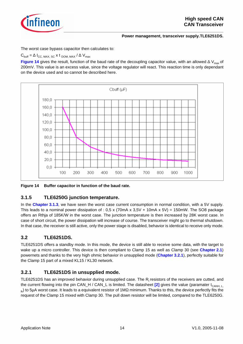
The worst case bypass capacitor then calculates to:Cbuff = ∆ ICC, MAX, SC x t DOM, MAX / ∆ Vmax
Figure 14 gives the result, function of the baud rate of the decoupling capacitor value, with an allowed ∆ Vmax of200mV. This value is an excess value, since the voltage regulator will react. This reaction time is only dependanton the device used and so cannot be described here.
Figure 14 Buffer capacitor in function of the baud rate.
3.1.5 TLE6250G junction temperature.In the Chapter 3.1.3, we have seen the worst case current consumption in normal condition, with a 5V supply.This leads to a nominal power dissipation of : 0,5 x (70mA x 3,5V + 10mA x 5V) = 150mW. The SO8 packageoffers an Rthja of 185K/W in the worst case. The junction temperature is then increased by 28K worst case. Incase of short circuit, the power dissipation will increase of course. The transceiver might go to thermal shutdown.In that case, the receiver is still active, only the power stage is disabled, behavior is identical to receive only mode.
3.2 TLE6251DS.TLE6251DS offers a standby mode. In this mode, the device is still able to receive some data, with the target towake up a micro controller. This device is then compliant to Clamp 15 as well as Clamp 30 (see Chapter 2.1)powernets and thanks to the very high ohmic behavior in unsupplied mode (Chapter 3.2.1), perfectly suitable forthe Clamp 15 part of a mixed KL15 / KL30 network.
3.2.1 TLE6251DS in unsupplied mode.TLE6251DS has an improved behavior during unsupplied case. The Ri resistors of the receivers are cutted, andthe current flowing into the pin CAN_H / CAN_L is limited. The datasheet [2] gives the value (paramater ICANH, L,
lk) to 5µA worst case. It leads to a equivalent resistor of 1MΩ minimum. Thanks to this, the device perfectly fits therequest of the Clamp 15 mixed with Clamp 30. The pull down resistor will be limited, compared to the TLE6250G.
Application Note 15 V1.0, 2005-11-08
High speed CANCAN Transceiver
Power management, transceiver supply.TLE6251G.
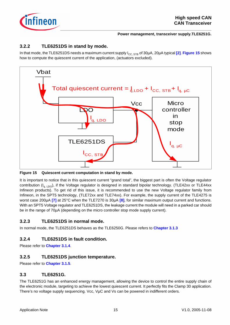
3.2.2 TLE6251DS in stand by mode.In that mode, the TLE6251DS needs a maximum current supply ICC, STB of 30µA, 20µA typical [2]. Figure 15 showshow to compute the quiescent current of the application, (actuators excluded).
Figure 15 Quiescent current computation in stand by mode.
It is important to notice that in this quiescent current “grand total”, the biggest part is often the Voltage regulatorcontribution (Iq, LDO), if the Voltage regulator is designed in standard bipolar technology. (TLE42xx or TLE44xxInfineon products). To get rid of this issue, it is recommended to use the new Voltage regulator family fromInfineon, in the SPT5 technology, (TLE72xx and TLE74xx). For example, the supply current of the TLE4275 isworst case 200µA [7] at 25°C when the TLE7270 is 30µA [8], for similar maximum output current and functions.With an SPT5 Voltage regulator and TLE6251DS, the leakage current the module will need in a parked car shouldbe in the range of 70µA (depending on the micro controller stop mode supply current).
3.2.3 TLE6251DS in normal mode.In normal mode, the TLE6251DS behaves as the TLE6250G. Please refers to Chapter 3.1.3
3.2.4 TLE6251DS in fault condition.Please refer to Chapter 3.1.4.
3.2.5 TLE6251DS junction temperature.Please refer to Chapter 3.1.5.
3.3 TLE6251G.The TLE6251G has an enhanced energy management, allowing the device to control the entire supply chain ofthe electronic module, targeting to achieve the lowest quiescent current. It perfectly fits the Clamp 30 application.There’s no voltage supply sequencing. Vcc, VµC and Vs can be powered in indifferent orders.
LDOMicro
controllerin
stopmode
TLE6251DS
Vcc
Vbat
Iq, LDO
Iq, µC
ICC, STB
Total quiescent current = I q,LDO + ICC, STB + Iq, µC

High speed CANCAN Transceiver
Power management, transceiver supply.TLE6251G.
Application Note 16 V1.0, 2005-11-08
3.3.1 TLE6251G in unsupplied mode.Same remarks as for the TLE6251DS, see Chapter 3.2.1.
3.3.2 TLE6251G in sleep mode.In sleep mode, the quiescent current of the device is 25µA typical, 35µA worst case on the Vs pin [3]. If the Vccand VµC are OFF, using the INH functionality (see also Chapter 4.3.8), then the entire module will need no morecurrent (actuators excluded).
Figure 16 Quiescent current computation in sleep mode, with and without inhibit functionnality.
In case the Vcc and / or VµC are supplied, an extra leakage current has to be taken into account, and the overallquiescent current of the module will increase dramatically. Figure 16 shows the two cases. The Iq, INH values aregiven in the data sheet and are typically in the range of one µA.
3.3.3 TLE6251G in Stand by mode.The stand-by mode is entered at power up or after under voltage as Vs. Compared to sleep mode, the TLE6251Gturns ON the high side switch of the INH output so an extra leakage current has to be taken into account. 25µAmaximum to turn ON and supply the high side internally [3]. It is also necessary to compute the extra current ofthe INH load which is connected to the INH output, which is application dependant.The TLE6251G includes a under voltage detection on its three supply pins, Vs, Vcc and Vµc. In case the applicationrequires to keep the device in standby mode for a long time (higher than the minimum under voltage blanking time,see also Chapter 4.3.5.2), then, both Vcc and VµC have to be present. Otherwise, the TLE6251G will goautomatically to sleep mode. It means the quiescent current of an application with TLE6251G remaining in standby mode is bigger than the sleep mode, since the voltage regulators must remains ON, even if no or few currentare consumed.
LDO
LDO
TLE6251G
Vbat
VµC
VCC
INH
INH
INH
µC
LDO
LDO
TLE6251G
Vbat
VµC
VCC
µC
Iq, INH
Iq, INH
Iq
Iq
IVS, sleep
Iq,µC
Icc+µC, sleepIVS, sleep

Application Note 17 V1.0, 2005-11-08
High speed CANCAN Transceiver
Power management, transceiver supply.TLE6251G.
3.3.4 TLE6251G in receive only mode.In receive only mode, the device is functional and needs the same current as in normal mode, recessive state.
3.3.5 TLE6251G in normal mode.In the normal mode, the TLE6251G behaves as the TLE6250G so please refers to Chapter 3.1.3, with the correctvalues given in the data sheet [3].
3.3.6 TLE6251G in fault condition.As for the TLE6250G and TLE6251DS, the current consumption on the Vcc pin will increase dramatically. Pleaserefer to chapter Chapter 3.1.4. Since the bus error management is only valid after four transitions of bus (fromrecessive to dominant), the worst case scenario with 17 consecutive bits dominant has to be taken into accountas well.
3.3.7 TLE6251G junction temperature.In normal condition, the device needs 40mA on the 5V Vcc supply. The SO14 package offers a RTHJA of maximum120K/W, leading to a junction temperature increase of 24K, compared to the ambient temperature.
3.3.8 Choice of the voltage regulator.The voltage regulator has to be chosen in the family of the low drop output (LDO), as the Infineon’s TLE42xx,TLE44xx, TLE72xx and TLE74xx. These LDOs families allow input voltage down to 5.5V at their input pin. To filterthe bounces on the battery supply line, the application requires a big input capacitor. This capacitor has to beprotected against reverse polarity by adding a diode. This diode has to be chosen with the lowest voltage drop(Schottky diode, typical 200mV) in its forward path. So to say that the LDO delivers a proper 5V with a minimumof 5.7V battery voltage. Below, the 5V cannot be warranted anymore, and the LDO follows the battery voltage. Forthe transceiver it means as well the level will be smaller, and follows the battery line, until a threshold when thecommunication will stop completly. It should be able to deliver 40mA DC current (see Chapter 3.1.3), only for thetransceiver. The LDO should also allow to work with a peak current of 105mA (see Chapter 3.1.4.1) for thetransceiver. Since the 105mA are not DC condition after a while, the Error Frame counter will stop thecommunication, it is not needed to warranty 105mA DC condition. The decoupling capacitor at the output of theLDO is described in Chapter 3.1.4.2. If the LDO is used only to supply the transceiver, the TLE4266-2G.[9],offering a minimun of 150mA peak current, an INH input, in SOT223, fits perfectly.

High speed CANCAN Transceiver
Interface with micro controller. TLE6250G/GV33.
Application Note 18 V1.0, 2006-04-01
4 Interface with micro controller.A CAN transceiver is the physical layer between the protocol controller (micro controller, state machine), to thephysical transmission medium. Following is a description, of TLE6250 and TLE6251 family, of the interfacebetween the micro controller and the Infineon’s used transceiver.
4.1 TLE6250G/GV33.Figure 17 shows the pin out and a brief description of the logic pins of the TLE6250G and TLE6250GV33, adaptedto 3.3V logic level. Following is a description of the logical pin and Figure 21 and Figure 22 gives the standardschematic of the application.
Figure 17 Block diagram of TLE6250G/ TLE6250GV33
4.1.1 Pin VccThe pin Vcc gives the proper 5V supply to build the CAN_H and CAN_L signal, as well as the receiver supply andinternal voltage reference supply to build the recessive state level. In case of TLE6250G use, the logic pins arepulled up to Vcc. Chapter 3.3.8 gives additional information about how to size correctly the voltage regulatorsupply.
TLE 6250 G
TLE6250G BLOCK DIAGRAM.VSD
Mode Control
TxD1
3 VCC
INH8
RM5
RxD4
TLE 6250 G V33
Mode Control
TxD1
INH8
RxD4
5 V33
Application Note 19 V1.0, 2006-04-01
High speed CANCAN Transceiver
Interface with micro controller. TLE6250G/GV33.
4.1.2 Pin RM (only for the TLE6250G version).The pin RM or Receive only Mode is a special feature from the TLE6250G. This pin allows to inhibit the datastreaming on the TxD pin, which blocks the transmission. Main functionality of the receive only mode is to allowdiagnostic (to avoid the aknowledge bit realized by software), to check modules connections, see Figure 18, or toavoid miss-communication on the medium due to a micro controller failure. To enter the Receive-only Mode, alogical zero has to be applied on the pin. To set the device in normal operation, so to activate the data streamingfrom the micro controller on the TxD pin, the RM pin has to be set to a logical 1. Since the TLE6250G integratesa pull up resistor, by default the device is in normal operation. In case the Receive only mode is not used, the pincan to be left opened.
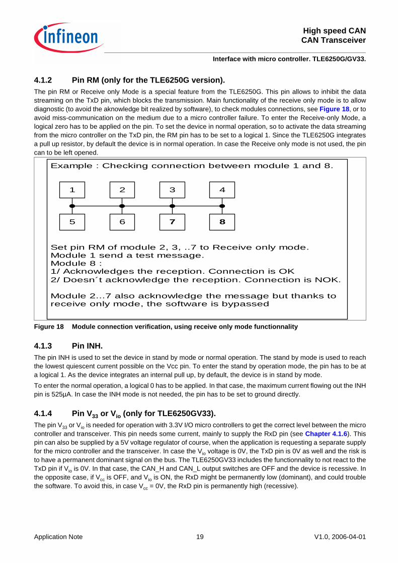
Figure 18 Module connection verification, using receive only mode functionnality
4.1.3 Pin INH.The pin INH is used to set the device in stand by mode or normal operation. The stand by mode is used to reachthe lowest quiescent current possible on the Vcc pin. To enter the stand by operation mode, the pin has to be ata logical 1. As the device integrates an internal pull up, by default, the device is in stand by mode. To enter the normal operation, a logical 0 has to be applied. In that case, the maximum current flowing out the INHpin is 525µA. In case the INH mode is not needed, the pin has to be set to ground directly.
4.1.4 Pin V33 or Vio (only for TLE6250GV33).The pin V33 or Vio is needed for operation with 3.3V I/O micro controllers to get the correct level between the microcontroller and transceiver. This pin needs some current, mainly to supply the RxD pin (see Chapter 4.1.6). Thispin can also be supplied by a 5V voltage regulator of course, when the application is requesting a separate supplyfor the micro controller and the transceiver. In case the Vio voltage is 0V, the TxD pin is 0V as well and the risk isto have a permanent dominant signal on the bus. The TLE6250GV33 includes the functionnality to not react to theTxD pin if Vio is 0V. In that case, the CAN_H and CAN_L output switches are OFF and the device is recessive. Inthe opposite case, if Vcc is OFF, and Vio is ON, the RxD might be permanently low (dominant), and could troublethe software. To avoid this, in case Vcc = 0V, the RxD pin is permanently high (recessive).
1 2 3 4
5 6 7 8
Example : Checking connection between module 1 and 8.
Set pin RM of module 2, 3, ..7 to Receive only mode.Module 1 send a test message.Module 8 :1/ Acknowledges the reception. Connection is OK2/ Doesn´t acknowledge the reception. Connection is NOK.
Module 2...7 also acknowledge the message but thanks toreceive only mode, the software is bypassed
High speed CANCAN Transceiver
Interface with micro controller. TLE6250G/GV33.
Application Note 20 V1.0, 2006-04-01
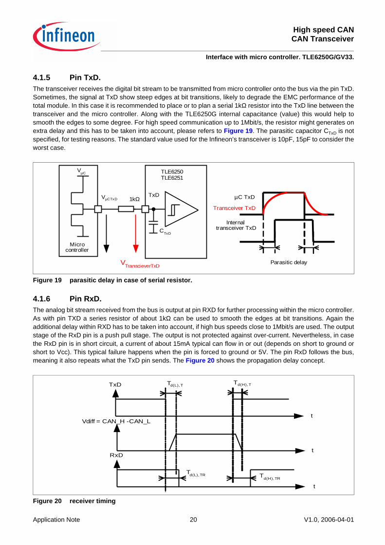
4.1.5 Pin TxD.The transceiver receives the digital bit stream to be transmitted from micro controller onto the bus via the pin TxD.Sometimes, the signal at TxD show steep edges at bit transitions, likely to degrade the EMC performance of thetotal module. In this case it is recommended to place or to plan a serial 1kΩ resistor into the TxD line between thetransceiver and the micro controller. Along with the TLE6250G internal capacitance (value) this would help tosmooth the edges to some degree. For high speed communication up to 1Mbit/s, the resistor might generates onextra delay and this has to be taken into account, please refers to Figure 19. The parasitic capacitor CTxD is notspecified, for testing reasons. The standard value used for the Infineon’s transceiver is 10pF, 15pF to consider theworst case.
Figure 19 parasitic delay in case of serial resistor.
4.1.6 Pin RxD.The analog bit stream received from the bus is output at pin RXD for further processing within the micro controller.As with pin TXD a series resistor of about 1kΩ can be used to smooth the edges at bit transitions. Again theadditional delay within RXD has to be taken into account, if high bus speeds close to 1Mbit/s are used. The outputstage of the RxD pin is a push pull stage. The output is not protected against over-current. Nevertheless, in casethe RxD pin is in short circuit, a current of about 15mA typical can flow in or out (depends on short to ground orshort to Vcc). This typical failure happens when the pin is forced to ground or 5V. The pin RxD follows the bus,meaning it also repeats what the TxD pin sends. The Figure 20 shows the propagation delay concept.
Figure 20 receiver timing
µC TxD1kΩ
Microcontroller
VµC
CTxD
VTranscieverTxD
VµCTxD
Transceiver TxD
Internaltransceiver TxD
TLE6250TLE6251
TxD
Parasitic delay
TxD
tVdiff = CAN_H -CAN_L
tRxD
t
Td(H), TRTd(L), TR
Td(H), TTd(L), T

Application Note 21 V1.0, 2006-04-01
High speed CANCAN Transceiver
Interface with micro controller. TLE6250G/GV33.
Figure 21 Typical application for TLE6250G
Figure 22 Typical application for TLE6250GV33.
e. g. TLE 4270
INH8
RxD4
TxD1
5RM
3GND
GND
VI
TLE 6250 G
VCC
VQ15 V
+
2
µP
GND
1kΩ (1)
(1) Optional, to improve EMCperformance
Main switch
Vbat
GPIO
GPIO
Some pins are missing, for simplification purposes
e. g. TLE 4476
INH8
RxD4
TxD1
5V33 V
3GND
GND
VI
TLE 6250 G V33
VCC
VQ15 V
+ +VQ2
3.3 V
3.3 V
2
µP
GND
1kΩ (1)
(1) Optional, to improve EMCperformance
Main switch
Vbat
Some pins are missing, for simplification purposes
High speed CANCAN Transceiver
Interface with micro controller. TLE6251DS.
Application Note 22 V1.0, 2006-04-01
4.2 TLE6251DS.Compared to the TLE6250G, TLE6251DS has almost the same pin out (see Figure 23). The TLE6251DS is ableto wake up the micro controller on bus activities. We will now describe the logic pins of the TLE6251DS. Figure 27describes the typical application interface between TLE6251DS and micro controller. TLE6251DS fits only to 5Vmicro controller interface.
Figure 23 Pin out comparison TLE6251DS and TLE6250G
4.2.1 Pin STB.The STB pin (STand By) is used to set the TLE6251DS in the standby or normal mode. To set the device to normaloperation, a logical 0 has to be applied. (and logical 1 to set the device to standby mode). As the pin has anintegrated pull-up, by default the device is in standby mode. In case the standby feature isn’t needed, the pinshould be connected to ground.
4.2.2 Pin TxD.
4.2.2.1 Hardware description.Please refers to the Chapter 4.1.5, description of the TxD of the TLE6250G.
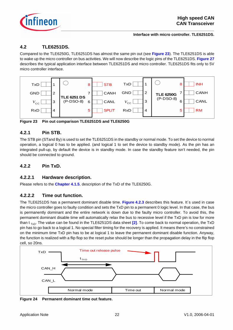
4.2.2.2 Time out function.The TLE6251DS has a permanent dominant disable time. Figure 4.2.3 describes this feature. It´s used in casethe micro controller goes to faulty condition and sets the TxD pin to a permanent 0 logic level. In that case, the busis permanently dominant and the entire network is down due to the faulty micro controller. To avoid this, thepermanent dominant disable time will automatically relax the bus to recessive level if the TxD pin is low for morethan t TxD. The value can be found in the TLE6251DS data sheet [2]. To come back to normal operation, the TxDpin has to go back to a logical 1. No special filter timing for the recovery is applied. It means there’s no constrainedon the minimum time TxD pin has to be at logical 1 to leave the permanent dominant disable function. Anyway,the function is realized with a flip flop so the reset pulse should be longer than the propagation delay in the flip flopcell, so 20ns.
Figure 24 Permanent dominant time out feature.
1TxD
2GND
3VCC
4RxD
8
7
6
5
CANH
CANL
STB
SPLIT
TLE 6251 DS(P-DSO-8)
1TxD
2GND
3VCC
4RxD
8
7
6
5
CANH
CANL
INH
RM
TLE 6250G(P-DSO-8)
Normal mode Time out Normal mode
TxD
CAN_H
CAN_L
tTX D
Time out release pulse

Application Note 23 V1.0, 2006-04-01
High speed CANCAN Transceiver
Interface with micro controller. TLE6251DS.
4.2.2.3 Time out function. Baud rate limitation.This feature limits the minimum possible baud rate. According to the CAN protocol a maximum of elevensuccessive dominant bits is allowed on TXD only (worst case of five successive dominant bits followedimmediately by an error frame). With a minimum value given in the data sheet for TxD of 300µs [2], so to say that11 bits should be faster than 300µs, the baud rate of the application must be higher than 36.6kbit/s to be sure tocomply to the CAN protocol. Min baud rate = max dominant bits / t TXD.
4.2.3 Pin RxD.
4.2.3.1 Hardware description.The RxD pin is as for the TLE6250G, see Chapter 4.1.6, a push pull stage. In case of short circuit to ground orVcc, the current is limited to maximum 20mA ( see datasheet [2] IscRxD).
4.2.3.2 Wake up behavior.The RxD pin is used to wake the micro controller up. To realize the wake up mechanism, the micro controllershould be in stop mode and the RxD pin should be an interrupt input in order to wake. Figure 25 gives the timingof the wake function. The parameter tWU is given in the data sheet of the TLE6251DS [2] and is directly copiedfrom the ISO 11898-5 norm[6]. It has to be understood as: 1. In case the pulse on the bus is shorter than the minimum value of tWU, the device will/has to never wake up.
This is to avoid parasitic wakes up due to Electro Magnetic disturbances for example.2. In case the pulse on the bus is in between the minimum value and the maximum value, the device might wake
up, depending on the temperature, production spread, etc....3. In case the pulse on the bus is longer than the maximum value of tWU, the device will/has to wake up.4. Since the application micro controller might missed the first edge, the TLE6251DS is following the bus toggling.
Figure 25 Wake up timing.
CAN_H
CAN_L
Stand by mode Normal mode
STB
RxD
tWU tWU
TLE6251DSstate
Stop mode Normal modeMicrocontrollerstate
Microncontroller Sets STB pin to 0
(1 and 2) Tooshort
wake pulse
Recessive level sets bythe module who wants to
wake the TLE6251DS
(4) Wake up pulse missedby microcontroller
tWU
tSTARTµC
Start up
3

High speed CANCAN Transceiver
Interface with micro controller. TLE6251DS.
Application Note 24 V1.0, 2006-04-01
4.2.3.3 Delay from stand by to normal mode.To achieve a very good quiescent current in standby mode, the TLE6251DS has two receivers, a low power modeand a normal mode. When the micro controller set the device to normal operation with the STB pin, and the busis dominant, a parasitic pulse on the RxD pin is observed. This is due to the commutation from the low powerreceiver to the normal receiver. Figure 26 describes the timing of this possible parasitic pulse. Unless this parasiticpulse maximum duration isn´t specified, it is never longer than 50µs.
Figure 26 Delay from stand by to normal mode timing.
Figure 27 Typical application for the TLE6251DS.
CAN_H
CAN_L
Stand by mode Transition Normal mode
STB
RxD
Parasitic TLE6251DS reset pulse
tWU
tWU
e. g. TLE 7270
STB8
RxD4
TxD1
3GND
GND
VI
TLE 6251DS
VCC
VQ15 V
+
2
µP
GND
1kΩ (1)
(1) Optional, to improve EMCperformance
Vbat
GPIO
GPIO
Some pins are missing, for simplification purposes
VCC
Application Note 25 V1.0, 2006-04-01
High speed CANCAN Transceiver
Interface with micro controller. TLE6251G.
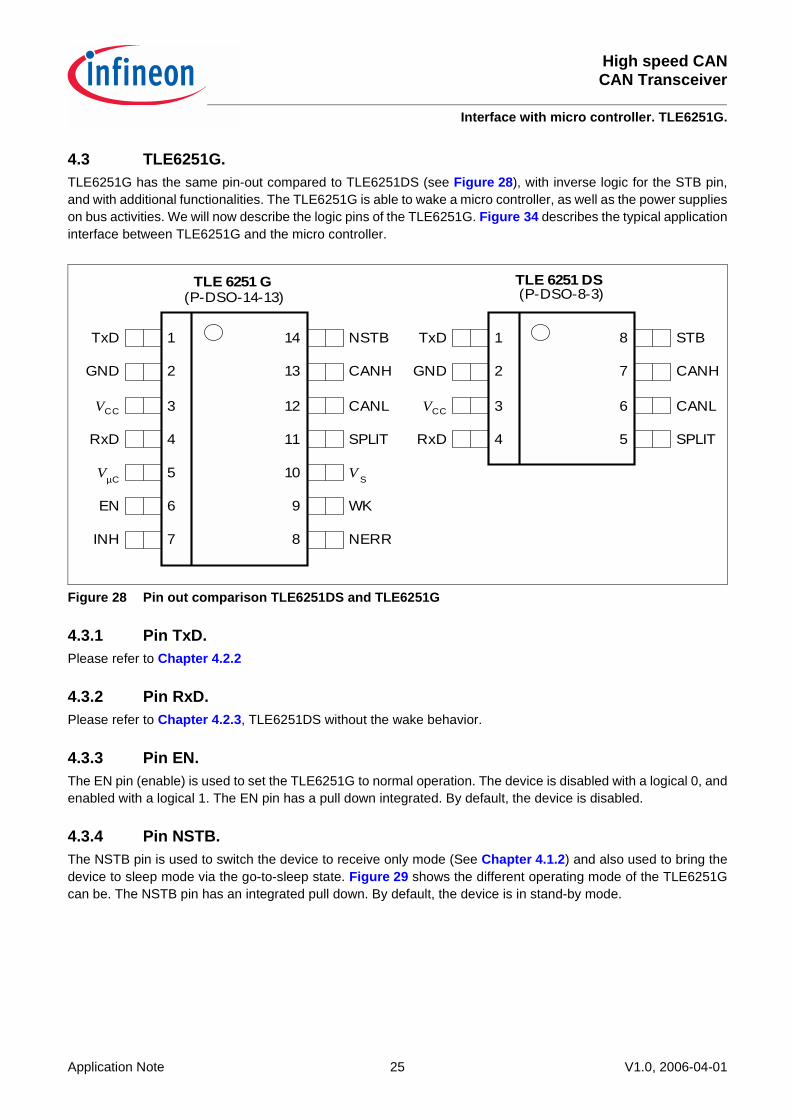
4.3 TLE6251G.TLE6251G has the same pin-out compared to TLE6251DS (see Figure 28), with inverse logic for the STB pin,and with additional functionalities. The TLE6251G is able to wake a micro controller, as well as the power supplieson bus activities. We will now describe the logic pins of the TLE6251G. Figure 34 describes the typical applicationinterface between TLE6251G and the micro controller.
Figure 28 Pin out comparison TLE6251DS and TLE6251G
4.3.1 Pin TxD.Please refer to Chapter 4.2.2
4.3.2 Pin RxD.Please refer to Chapter 4.2.3, TLE6251DS without the wake behavior.
4.3.3 Pin EN.The EN pin (enable) is used to set the TLE6251G to normal operation. The device is disabled with a logical 0, andenabled with a logical 1. The EN pin has a pull down integrated. By default, the device is disabled.
4.3.4 Pin NSTB.The NSTB pin is used to switch the device to receive only mode (See Chapter 4.1.2) and also used to bring thedevice to sleep mode via the go-to-sleep state. Figure 29 shows the different operating mode of the TLE6251Gcan be. The NSTB pin has an integrated pull down. By default, the device is in stand-by mode.
7
6
5
4
3
2
1TxD
GND
VCC
RxD
VµC
EN
INH 8
9
10
11
12
13
14
CANH
CANL
SPLIT
WK
NERR
NSTB
V S
TLE 6251 G(P-DSO-14-13)
1TxD
2GND
3VCC
4RxD
8
7
6
5
CANH
CANL
STB
SPLIT
TLE 6251 DS(P-DSO-8-3)

High speed CANCAN Transceiver
Interface with micro controller. TLE6251G.
Application Note 26 V1.0, 2006-04-01
Figure 29 TLE6251G Mode state diagram
4.3.5 Pin VµC.The VµC pin is used to supply the pins in direct contact with the micro controller, to get the voltage reference of themicro controller threshold, in order to use the device both with 3.3V and 5V micro controller. In case the microcontroller has the same supply as the CAN transceiver, the VµC and Vcc should be connected together.
4.3.5.1 VµC pin´s maximum current.The push-pull for the RxD, as well as the NERR pin are supplied by VµC. In case the RxD pin and/or the NERRare in short circuit to ground, a non-negligible current (please refers to TLE6251G data sheet [3], ISC_NERR, ISC_RxD)will be demanded to the micro controller supply.
4.3.5.2 Vµc under voltage detection.The VµC voltage level is monitored by the TLE6251G. Benefit of this solution is to avoid any undesiredcommunication on the bus when Vcc is present but the micro controller is down. In case of under voltage detectionon pin VµC, the device is going to sleep mode. Since the device can command the micro controller supply, with the
TLE6251G STATE DIAGRAM.VSD
EN NSTB INH1 1 High
Normal Mode
Undervoltageat VCC /VµCfor t > tUV,t
EN NSTB INH0 0 High
Stand-By
Undervoltageat VS
t < thS LP
t > thS LP
Wake-Up:t > tWKt > tWU
EN NSTB INH0 0 Float.
Sleep
Start UpPower UpPower Down
EN NSTB INH0 1 High
Receive-OnlyGo to Sleep
NSTBEN01
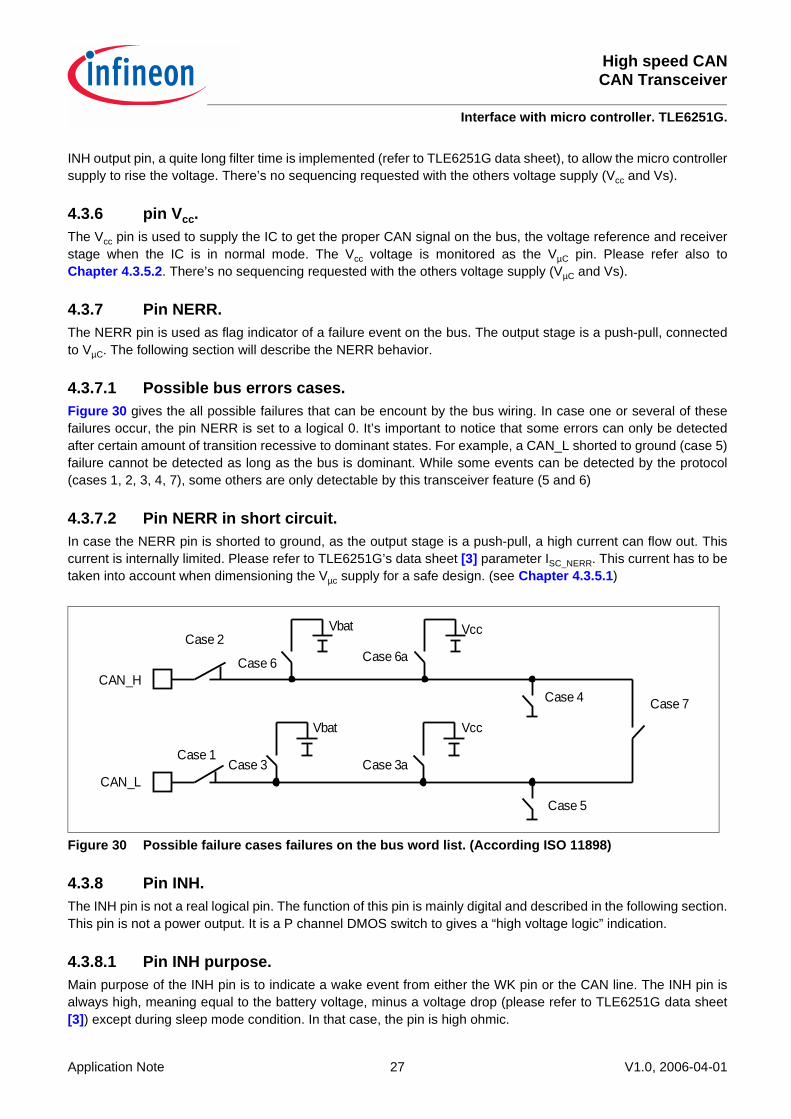
Application Note 27 V1.0, 2006-04-01
High speed CANCAN Transceiver
Interface with micro controller. TLE6251G.
INH output pin, a quite long filter time is implemented (refer to TLE6251G data sheet), to allow the micro controllersupply to rise the voltage. There’s no sequencing requested with the others voltage supply (Vcc and Vs).
4.3.6 pin Vcc.The Vcc pin is used to supply the IC to get the proper CAN signal on the bus, the voltage reference and receiverstage when the IC is in normal mode. The Vcc voltage is monitored as the VµC pin. Please refer also toChapter 4.3.5.2. There’s no sequencing requested with the others voltage supply (VµC and Vs).
4.3.7 Pin NERR.The NERR pin is used as flag indicator of a failure event on the bus. The output stage is a push-pull, connectedto VµC. The following section will describe the NERR behavior.
4.3.7.1 Possible bus errors cases.Figure 30 gives the all possible failures that can be encount by the bus wiring. In case one or several of thesefailures occur, the pin NERR is set to a logical 0. It’s important to notice that some errors can only be detectedafter certain amount of transition recessive to dominant states. For example, a CAN_L shorted to ground (case 5)failure cannot be detected as long as the bus is dominant. While some events can be detected by the protocol(cases 1, 2, 3, 4, 7), some others are only detectable by this transceiver feature (5 and 6)
4.3.7.2 Pin NERR in short circuit.In case the NERR pin is shorted to ground, as the output stage is a push-pull, a high current can flow out. Thiscurrent is internally limited. Please refer to TLE6251G’s data sheet [3] parameter ISC_NERR. This current has to betaken into account when dimensioning the Vµc supply for a safe design. (see Chapter 4.3.5.1)
Figure 30 Possible failure cases failures on the bus word list. (According ISO 11898)
4.3.8 Pin INH.The INH pin is not a real logical pin. The function of this pin is mainly digital and described in the following section.This pin is not a power output. It is a P channel DMOS switch to gives a “high voltage logic” indication.
4.3.8.1 Pin INH purpose.Main purpose of the INH pin is to indicate a wake event from either the WK pin or the CAN line. The INH pin isalways high, meaning equal to the battery voltage, minus a voltage drop (please refer to TLE6251G data sheet[3]) except during sleep mode condition. In that case, the pin is high ohmic.
Vbat Vcc
Vbat Vcc
Case 1
Case 2
Case 6 Case 6a
Case 7
Case 5
Case 4
Case 3 Case 3a
CAN_H
CAN_L

High speed CANCAN Transceiver
Interface with micro controller. TLE6251G.
Application Note 28 V1.0, 2006-04-01
4.3.8.2 Pin INH power capability.The pin is not suitable to drive a low ohmic load, and the output current should not exceed 5mA. It is thenimpossible to drive the input of a voltage regulator (LDO) directly but should be used to drive the inhibit input ofthe LDO. The INH input isn’t protected against short circuit to ground and so should not be connected outside theE.C.U. In the case of a short to ground, or overload, the protection will be the thermal shutdown.
4.3.8.3 Pin INH driving the INH input of an Voltage regulator.All Infineon LDO family are active when their INH input is high and OFF when the INH input is low. Since they allhave an integrated pull down, it´s normally not necessary to add an external one. Anyway, for EMC issue, it´sreasonable to plan an external resistor with a value of 10kΩ, in case of parasitics coming into the INH pin.Figure 31 shows the recommended circuitry for the pin INH.
Figure 31 Circuitry for the INH output
4.3.8.4 Wake up timing with pin INH.Using the INH pin to drive the voltage regulator INH, the wake up timing is shown on Figure 33. Please note thetime scale isn’t linear. The start up of a voltage regulator takes several ms when the logical signal are in ns. Insome applications, only the inhibit input of the micro-controller voltage regulator, or the voltage regulator for theCAN transceiver is driven by theTLE6251G. The Vcc line necessary for proper supply of the transceiver, or theVµC for proper supply of the micro-controller is switched on by the micro-controller. If we assume a 2ms activationtime for each LDO ( see Equation (4)), and the necessary start-up time of the microcontroller, the time to go tonormal operation increased significantly, like 10 to 40ms normally. Whenever this time is below 50ms (see [3],parameter t UV,t), the undervoltage mechanism is inhibited. It gives the time to react without entering into the sleepmode again, which will inhibit the microcontroller LDO and so entering infinite cyclic wakes.Start up time of an Voltage regulator formula:
Tmax = Cmax x Vcc /(Imin- I start_up) (4)
Tmax represents the longest time needed to reach the regulated voltage (5 or 3.3V)Cmax is the total capacitance on the regulated voltage. (With capacitance tolerance)Vcc is the regulated voltage (5 or 3.3V)Imin is the minimum current the voltage regulator is able to drive as maximum.
INH
10kΩ optional
VBAT
Vs INH
TLE6251G
TLE4xxxTLE7xxx
LDO

Application Note 29 V1.0, 2006-04-01
High speed CANCAN Transceiver
Interface with micro controller. TLE6251G.
Istart_up is the current the application (e.g micro controller) need during start up phase.Example, with the TLE4278G. The TLE4278G is a 5V Voltage regulator. Data sheet [4] specifies a minimum value for the maximum current theVoltage regulator is able to drive of Imin = 200mA. Assuming :CMAX = 60µF (20% tolerance on a 47µF capacitor) decoupling capacitors on the Vcc, Istart_up = 20mA to supply the application (microcontroller, logical circuitries...) the maximum time the Voltageregulator needs to reach 5V, starting from 0V is then: Tmax = 60 x10-6 x 5 / (200 10-3 - 20 10-3)= 1,7ms.
4.3.9 pin WK.The WK pin (Wake) is also a high voltage pin. It is used mainly to signal a local wake up event on the transceiver.A signal change is only necessary to wake up the device. There´s no pull-up or pull-down, so it can be used towake via a switch to ground, or via a switch to battery. The wake up pin is sensible to voltage edges. In case theWake pin is unused, it is recommended to connect the pin directly to ground. (to avoid parasitic wake up). SeeFigure 32 for possible usage description.
Figure 32 Possible wake up circuitries.
RWK should be planned, to improve the robustness to ISO pulses. If the ISO pulses test shows good resultswithout, RWK is useless, because the absolute maximum rating (see [3]) allows enough safety margin. RSW isnecessary, to polarize the WK pin to the sleeping state. The value of RSW should be set according to the cleaningcurrent of the switch.
Vbat
WK switchTLE6251GWK
RWK*
RSW
Low side wake up
Vbat
WK switch
TLE6251GWK
RWK*
RSW
High side wake up
(*) optionnal

High speed CANCAN Transceiver
Interface with micro controller. TLE6251G.
Application Note 30 V1.0, 2006-04-01
Figure 33 Wake up timing with INH function. Cold start.
CAN_HCAN_L
Vdiff
INH
Vcc/Vio
RxD
NERR
NSTB/EN
µC P.O.R.
Normal mode
tWU
BUSOFF
BUSWAIT
WAKEPATTERN
DEVICEWAKES
ECU WAKESLDO RAMP UP
Communicationstarts
µC sets TLE6251G tonormal operation

Application Note 31 V1.0, 2006-04-01
High speed CANCAN Transceiver
Interface with micro controller. TLE6251G.
Figure 34 Typical application circuit for TLE6251G, with separate 3.3V VµC and 5V Vcc supply
CANcontroller
EN
NSTB
NERR
TxD
GPIO
GPIO
IRQ
TxD1kΩ (1)
RxDRxD
1kΩ (1)
Vµc
Vµc
Vµc
Vs
Vs
E.gTLE4266
INHINH
Vcc
E.gTLE7273GV33
INHVµc
10kΩ (1)
(1) Optional. To improve EMC performance
TLE6251G
Microcontroller with on chip CAN module
e.g C164, C167XC164TC17xx
CVcc
CVµC
CVs
µC supply

High speed CANCAN Transceiver
Interface with micro controller. TLE6251G.
Application Note 32 V1.0, 2006-04-01
4.3.10 Software issues consideration for TLE6251G.
4.3.10.1 Cold start.The power ON flag of the TLE6251G indicates to the microcontroller whether a microcontroller cold start wascaused by a wakeup from Sleep mode or by a first battery power application. This information is often needed forthe application to initiate some possible calibration procedures upon first battery power application.The pin NERR reflects the power ON flag when entering the power ON /Receive only mode from stand by, sleepor go to sleep mode. Moreover, in case of wake up from Sleep Mode, the TLE6251G provides information on thewake up source. Entering the Normal mode the pin NERR reflects the wake up source flag. A logical 0 signalindicates a local wake up via the WK pin whereas a logical 1 indicates a remote wakeup via the bus.In case battery power is applied the first time, an internal hardware reset is given to the transceiver for initialization.Subsequently, the power ON flag is set and the pin INH is pulled to Vbat, activating the voltage regulator(s) andramping up the Vcc supply. See also Chapter 4.3.8. Along with the Vcc the pins RxD and NERR go to logical 1.With ramping up Vcc, the micro controller comes up. As almost all micro controllers feature a weak pull down orfloating behaviour at their port pins, the TLE6251G comes up in stand by mode after first battery power up. Seealso Chapter 4.3.2 and Chapter 4.3.7. This is the starting point for the application program taking over the controlnow. If the microcontroller comes up with a logical 1 at its port pins, the TLE6251G enters the normal mode andthe power ON flag information is irretrievably lost. Please refer to the Figure 33 for timing characteristics.Figure 35 suggests a software flow for an ECU cold start. It considers primarily the issues related to theTLE6251G rather than representing a complete software flow. After the transceiver and microcontroller haveperformed their initialization, the transceiver is put in power ON / Receive Only Mode for reading the power ONflag. If a logical 0 signal is read on the pin NERR, the ECU cold start was initiated by the first battery power up.The microcontroller performs the correspnding system startup procedure. If a logical 1 is read, the cold start wasinitiated by a wake up from sleep mode. In order to get information on the wake up source, the Normal mode isselected. If reading of the pin NERR yields a logical 0, there was a local wake up via the pin wake. If reading yieldsa logical 1 signal, the wake up came via the bus. Afterwards, the cold start procedure is finished and normaloperation is ongoing.
4.3.10.2 Hot start.A warm start up is performed when the ECU wakes up from Sleep Mode. Figure 36 suggests a software flow foran ECU warm start. The starting point assumes a TLE6251G transceiver in its Sleep Mode and the hostmicrocontroller in a dedicated power down mode. If the transceiver receives a wake up either via the pin WK, theinternal wake up flag is set and signalled at the pin NERR and RxD. These signals can be used for wakeup of themicrocontroller from its power down mode. The starting application program can now take control over thetransceiver. If the power ON flag is of interest, the microcontroller can force the transceiver into Power ON /Receive Only Mode for reading the Power ON flag. Otherwise the microcontroller can force the transceiver directlyinto Normal mode for reading the wake up Source flag at the pin NERR.As the microcontroller remains powered by the Vcc supply, the microcontroller can monitor its port pins for possiblewake up events. Upon detection of a wake up event the microcontroller can initiate a wakeup by forcing thetransceiver directly into normal mode. Then reading of the Power ON flag or wake up Source, flag is not necessary.
4.3.10.3 Enter the Standby mode.When the network management decides to put the bus system into standby, each ECU must receive theappropriate standby command. The flow diagram seen in Figure 37 shows the different steps in order to put theTLE6251G into Standby mode. Upon receiving a standby command (like a CAN message), the microcontrollerhas to stop all CAN transmission. In order to ensure that no CAN communication is present on the bus anymore,caused by other nodes, the bus must have been recessive for a suitable time before the TLE6251G is put inStandby Mode by setting NSTB and EN to logical 0. If there is no system dependant “waiting period”, implementedthere would be the risk that a node sends out a last message while another one is already on the way towards

Application Note 33 V1.0, 2006-04-01
High speed CANCAN Transceiver
Interface with micro controller. TLE6251G.
Standby mode. This would cause a wake up event thus making it impossible to enter a system wide low powerstate.
4.3.10.4 Enter the Sleep mode.The procedure to put an ECU into sleep mode is shown in Figure 38 it is similar to the previous one for enteringthe Standby mode. Upon receiving a sleep command the microcontroller has to stop all CAN transmission. In orderto ensure that no CAN communication is present on the bus anymore, the bus must have been recessive forsuitbale time before the TLE6251G is put into Sleep Mode by selecting NSTB to logical 0 and EN to logical 1. Thedifference now is that the microcontroller checks periodically for a wake up as long as Vcc is not yet down. This isnecessary since it might happen that a wake up event just appears while the Go To Sleep Command is processed.In this case the INH of the TLE6251G will keep high and the Vcc will not drop down. Instead the wake up requestis forwarded to the application via RxD and NERR. Without this check the microcontroller would assume that asleep phase follows with disabled Vcc, thus waiting forever for a power ON reset caused by a wakeup which willnever happen.

High speed CANCAN Transceiver
Interface with micro controller. TLE6251G.
Application Note 34 V1.0, 2006-04-01
Figure 35 Flow diagram for an ECU cold start.
Cold Start
Set NSTB to 1EN to 0
Wait 10µs
Read NERR
NERR = 0
Set NSTB to 1
Wait 10µs
Read NERR
End of Cold Start
VBAT and GND connectedINH = High
NSTB, EN held LOWduring the Vcc ramping up
Selectpower ON/ Receive only mode
Power ON flag0 = First Vbat application
1= Wake up from Sleep mode
System start upprocedure
Set NSTB to 1EN to 1
Yes (first Vbat app)
No (sleep wake)
Select normal mode
Wake up source flag0 = local wake up1 Wake up via bus
OptionalIf power ON flag is not an interest
OptionalIf wake originis not an interest
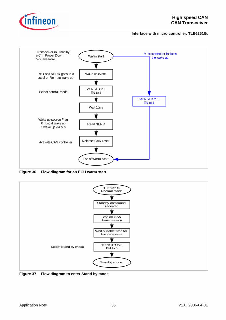
Application Note 35 V1.0, 2006-04-01
High speed CANCAN Transceiver
Interface with micro controller. TLE6251G.
Figure 36 Flow diagram for an ECU warm start.
Figure 37 Flow diagram to enter Stand by mode
Warm start
Wake up event
Set NSTB to 1EN to 1
Wait 10µs
Release CAN reset
End of Warm Start
Transceiver in Stand byµC in Power DownVcc available.
RxD and NERR goes to 0Local or Remote wake up
Select normal mode
Set NSTB to 1EN to 1
Activate CAN controller
Read NERRWake up source Flag
0 : Local wake up1 wake up via bus
Microcontroller initiatesthe wake up
TLE6251GNormal mode
Standby commandreceived
Stop all CANtransmission
Wait suitable time forbus recessive
Standby mode
Set NSTB to 0EN to 0Select Stand by mode
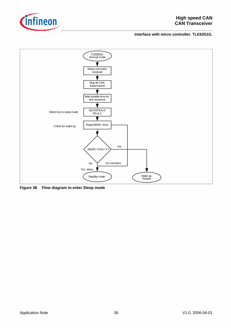
High speed CANCAN Transceiver
Interface with micro controller. TLE6251G.
Application Note 36 V1.0, 2006-04-01
Figure 38 Flow diagram to enter Sleep mode
TLE6251GNormal mode
Sleep commandreceived
Stop all CANtransmission
Wait suitable time forbus recessive
Standby mode
Set NSTB to 0EN to 1Select Go-to sleep mode
Read NERR / RxDCheck for wake up
NERR / RxD= 0 ?
Vcc not down.
Wake upRestart
Yes
No
Vcc down.

Application Note 37 V1.0, 2006-04-01
High speed CANCAN Transceiver
Bus pins. Terminations concepts. Termination resistors.
5 Bus pins. Terminations concepts.The transceiver is connected to the bus via the pin CAN_H and CAN_L. Some concept also includes a so calledSPLIT pin. The purpose of this pin is to improve EMC behavior of transceiver, by increasing the symmetry betweenCAN_H and CAN_L. See Figure 1.
5.1 Termination resistors.The ISO 11898-2 [5] and ISO 11898-5 [6] request for the system a 60Ω resistor bus termination. This bustermination resistor is needed to reduce the reflexions on the bus. Where and how to apply this 60Ω resistor is upto the OEM, several concepts are possible and used today, depending on the usage, the topology, etc... Someapplications have only one termination resistor, mainly for stars topology. Some applications have two terminationresistors of 120Ω, for linear topology, and some even have one termination resistor on each nodes, the totalimpedance should be equaled to 60Ω. However, it is recommended to put a weak termination resistor of 1kΩ atleast for EMC improvements of the system, in terms of emission. It is important to not forget the short circuit issue,described in the Chapter 2.3.4.1.
5.2 Split pin.The recommended application circuitry is described on Figure 39.
Figure 39 Application circuitry for the split pin.
5.2.1 Recessive voltage in a mixed Clamp 15 / 30 network, without SPLIT.When the system requires two types of modules, some connected to the CL15 (see Chapter 2.1.1), someconnected to the CL30 (see Chapter 2.1.2), the unsupplied modules bring to the bus an extra impedance toground. The result is the recessive voltage tends to go to 0V. The recessive voltage with a mixed network, without split pin can be computed with the Equation (5), with theusage of the TLE6250G.
Vrec = Vref x m / (m+n) (5)
m represents the number of nodes supplied and enable (CL30)n represents the number of unsupplied nodes. (CL15)Vref is the recessive voltage when the device is alone. See Table 1. Typically Vcc / 2The equivalent DC electrical schematic of the system is given on Figure 40, assuming (for simplification) allinternal impedances and voltage regulators identical. Figure 42 gives the voltage value, for m=2, function of n.
TLE6251GTLE6251DS
60Ω
60Ω
4.7nF (1)TLE6251GTLE6251DS
1kΩ (1)
1kΩ (1)
4.7nF (1)
(1) Suggested value, has to be according to the car maker requirements.
CAN_H
CAN_L
SPLIT
CAN_H
CAN_L
SPLIT

High speed CANCAN Transceiver
Bus pins. Terminations concepts. Split pin.
Application Note 38 V1.0, 2006-04-01
Figure 40 Equivalent electrical schematic for a mixed network without split pin
5.2.2 Recessive voltage in a mixed Clamp 15 / 30 network, with SPLIT.TLE6251DS and TLE6251G integrate a SPLIT pin. The internal schematic of the split pin is quite complex, but canbe simplified as a voltage regulator at VSPLIT with an internal resistor RSPLIT, [2] [3]. The purpose of the SPLIT pinis to improve the symetry of the signal, by maintaining the recessive voltage at mid value of the dominant voltageof CAN_H and CAN_L.
Using the SPLIT pin, the equivalent DC circuitry looks like Figure 41. The recessive voltage with a mixed network,with SPLIT pin can be computed with the Equation (6), assuming all devices identical (for simplificationpurposes).
Figure 41 Equivalent electrical schematic for a mixed network with SPLIT pin
m represents the number of supplied and enabled nodes with and without split pin.(min 2)t represents the number of SPLIT nodes with RT = 60Ω termination resistors (min 0, max 2)s represents the number of SPLIT nodes with RW > 1kΩ weak termination resistors
VRef OV
RCM
RCM
RCM
RCM
R termination total60 Ohm=120Ohm//120Ohm
m nodes n nodes
VRefOV
RCM
RCM
RCM
RCM
RT
m nodes n nodes
RSPLIT
VSPLIT
t nodes
RSPLIT
RW
VSPLIT
s nodes
RW
RT
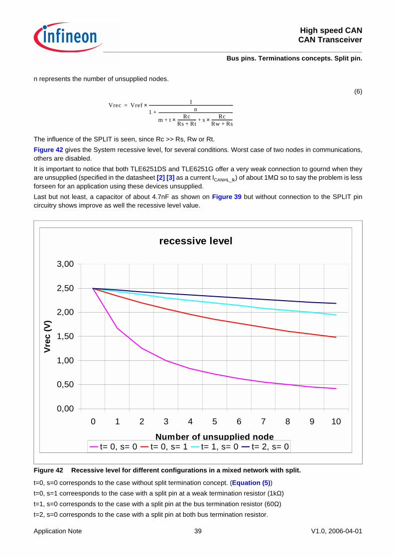
Application Note 39 V1.0, 2006-04-01
High speed CANCAN Transceiver
Bus pins. Terminations concepts. Split pin.
n represents the number of unsupplied nodes.
(6)
The influence of the SPLIT is seen, since Rc >> Rs, Rw or Rt.Figure 42 gives the System recessive level, for several conditions. Worst case of two nodes in communications,others are disabled.It is important to notice that both TLE6251DS and TLE6251G offer a very weak connection to gournd when theyare unsupplied (specified in the datasheet [2] [3] as a current ICANHL_lk) of about 1MΩ so to say the problem is lessforseen for an application using these devices unsupplied.Last but not least, a capacitor of about 4.7nF as shown on Figure 39 but without connection to the SPLIT pincircuitry shows improve as well the recessive level value.
Figure 42 Recessive level for different configurations in a mixed network with split.
t=0, s=0 corresponds to the case without split termination concept. (Equation (5))t=0, s=1 correesponds to the case with a split pin at a weak termination resistor (1kΩ)t=1, s=0 corresponds to the case with a split pin at the bus termination resistor (60Ω)t=2, s=0 corresponds to the case with a split pin at both bus termination resistor.
Vrec Vref 1
1 n
m t RcRs Rt+-------------------× s Rc
Rw Rs+---------------------×+ +
---------------------------------------------------------------------------+-------------------------------------------------------------------------------------×=
recessive level
0,00
0,50
1,00
1,50
2,00
2,50
3,00
0 1 2 3 4 5 6 7 8 9 10
Number of unsupplied node
Vrec
(V)
t= 0, s= 0 t= 0, s= 1 t= 1, s= 0 t= 2, s= 0

High speed CANCAN Transceiver
Bus pins. Terminations concepts. CAN_H / CAN_L.
Application Note 40 V1.0, 2006-04-01
5.3 CAN_H / CAN_L.The CAN_H and CAN_L are the interface to the bus network. The challenge for these pins are multiples. EMC,ESD, that we will see in Chapter 6 and Chapter 7. The challenge is also regarding short circuit discussed in theChapter 3.1.4 mainly. Last but not least, the CAN_H and CAN_L have parasitic capacitors to ground, due to theDMOS cells as well as the ESD structure. These parasitics capacitors are not specified, due to testing issues butthe maximum observed value are in the range of 50pF for CAN_H, half of it for CAN_L for the TLE6250G. Thereason for this unsymmetry is that CAN_L is a N channel, when the CAN_H is a P channel output stage. As a ruleof thumb, the P channel cell is twice bigger to get the same Rdson.

Application Note 41 V1.0, 2006-04-01
High speed CANCAN Transceiver
ESD Aspects. ESD tests definition.
6 ESD Aspects. Among all the disturbances a CAN transceiver can encounter in a vehicle, the ESD discharge is one of the mostcritical. Since the basic application of networking is to be present in the whole vehicle, the risk of ESD dischargeis very important. To get an impression of the issue, the Figure 43 shows the current flowing into the TLE6250G,function of the ESD HBM discharge voltage; The ESD pulse is applied on the CAN_H pin, and the current ismeasured on the ground line. The device is unsupplied. ESD robustness is strongly dependant to the air humiditycondition. ESD robustness is increasing with air humidity.
Figure 43 Current flowing in the TLE6250G ground, function of the ESD voltage. Device unsupplied
6.1 ESD tests definition.
6.1.1 Human Body Model test. (MIL-STD 883).The HBM test is a modification of the Method 3015.7, MIL-STD-883. The test is realized on one pin, versus all theothers. The semiconductor industry is keen to specify the ESD with HBM, because it represents the typicalaggression during the processing of the module, of the operator in the facility touching the device. The model isequivalent to a capacitor of 100pF loaded to the ESD voltage. The discharge is applied via a 1.5kΩ resistor (1500Ωis your standard resistance value...). This test doesn´t represents the normal ESD aggression during the life of thevehicle or during the car manufacturing, because the risk of somebody touching the device when the module isbuilt is very low. Figure 45 shows the test protocol. Infineon realize the HBM test inhouse. The HBM values arespecified in all Infineon’s datasheet. The standard value is +/-2kV, but can reach higher values for the off boardpins.
6.1.2 Gun test. (IEC 61000-4-2).The IEC 61000-4-2 ESD test represents the typical case of somebody carrying a metallic object (screw drivers,pliers...),touching the connectors or the housing of the module. It´s also called gun or pistol test. It applies the same

High speed CANCAN Transceiver
ESD Aspects. ESD tests definition.
Application Note 42 V1.0, 2006-04-01
voltage, as the HBM but loaded into 150pF and discharged via 330Ω. This test is more representative of the realESD disturbance during the car manufacturing. The Figure 44 shows the difference between the HBM and thegun test, for same voltage level. It´s obvious that the IEC61000-4-2 is a much more severe test in terms of energy.The test is realized on all the off board pins (CAN_H, CAN_L, Wake and Vs pin) versus ground. Figure 45 showsthe test protocol. For communication applications, as CAN and LIN physical layer, Infineon is performing the testin an external independant test facility (I.B.E.E. in Zwickau, Germany). The value isn’t specified in the Infineon’sdatasheet, because the test is also application’s dependant. Values reached can be given, on request.
Figure 44 Comparison of the current between HBM and gun test.
Figure 45 ESD test equipement
6.1.3 Charged Device Model (CDM).A device may also become charged. If it then contacts the insertion head or another conductive surface, a rapiddischarge may occur from the device to the metal object. This event is known as the Charged Device Model (CDM)event, and can be more destructive than the HBM for some devices. Although the duration of the discharge is veryshort (often less than one nanosecond) the peak current can reach several tens of Ampere.
5
10
15
20
25
30
I (A)
T (ns)
+8kV applied
30 60 90 120 150
IEC1000-4-2
1ns
HBM
D.U.T
R
CHBM
IEC
1500 Ω
330 Ω
100pF
150pF
R C

Application Note 43 V1.0, 2006-04-01
High speed CANCAN Transceiver
ESD Aspects. ESD protection.
6.1.4 Machine Model (MM).A discharge similar to the HBM event also can occur from a charged conductive object, such as a metallic tool orfixture. Originating in Japan as the result of trying to create a worst-case HBM event, the model is known as theMachine Model. This ESD model consists of a 200pF capacitor discharged directly into a component with no seriesresistor. As a worst-case human body model, the Machine Model may be over severe. However, there are real-world situations that this model represents, for example the rapid discharge from a charged board assembly orfrom the charged cables of an automatic tester.
6.2 ESD protection.All infineon’s product includes an internal ESD protection. The concept of the Infineon’s ESD protection differsfrom the others silicon supplier. The ESD protection is turned ON as soon as the voltage reach a certain values.This values is actually specified in the datasheet [1], [2]and [3], as the absolute maximum rating. The avalanchevoltage of the technology has to be higher than the ESD protection threshold. The Figure 46 shows the ESD proctection behavior. The standard protection is the most commonly used bysemiconductors suppliers. The improved ESD protection is the typical behavior of the ESD protection all newInfineon’s transceiver includes. Compared to the standard protection, it reduces the energy and heat into thedevice. Moreover, the Infineon’s SPT technology allows low thermal resistance to the leadframe. The heat is thenspread into the whole device, reducing the risk of hot spots (local overheat).
Figure 46 Standard and Infineon ESD protection
6.3 Modules under ESD gun test.Figure 47 shows the test set up for the following section, with the respective external component.
I (A)
V
TLE6251DSTLE6251G
ESD protection
Ideal ESD protection
Standard ESD protectionTLE6250G
Symbolic representation ofthe ESD protection
Snap back parasitic effect

High speed CANCAN Transceiver
ESD Aspects. Modules under ESD gun test.
Application Note 44 V1.0, 2006-04-01
Figure 47 Schematic of the test
6.3.1 Device without any external protection circuitry.The Figure 48 and Figure 49 shows the measurement realized at the ground line and Vcc line (device is suppliedto the 5V), with 1kV gun test for the TLE6250G. The ESD discharge is applied on CAN_H.
Figure 48 Positive ESD discharge, device supplied. Read out of the ground and supply current.
Receiver
OutputStage
Driver
Temp.-Protection
6
CANH
CANL
Vcc
7
3
1TxD
RxD
4
2GND
TLE 6250 G
ModeControl
8INH
5
RMVCC
(*) Shunts for current measurements
*
*
**

Application Note 45 V1.0, 2006-04-01
High speed CANCAN Transceiver
ESD Aspects. Modules under ESD gun test.
Figure 49 Negative ESD discharge, device supplied. Read out of the ground and supply current.
6.3.2 ESD level reached with a choke coil.The purpose of the choke coil is described in the Chapter 7. The Figure 50 shows the typical current flowing intothe ground line during the ESD discharge. The measurements show that the choke coil has no real influence onthe results and could not be considered as an efficient solution for ESD protection.
Figure 50 ESD discharge, device supplied. Read out of the ground current. With choke coil.
6.3.3 ESD level reached with a choke coil and ESD diode or varistor.The Figure 51 and Figure 52 show the results on an ESD positive and negative discharges on the pin CAN_H,device supplied. The influence is clearly seen, when using both varistor and choke coil. Using the varistor alonedoesn’t influence too much the results, because the varistor isn’t fast enough. Using these external components,
Without coil
B82790S513 (Epcos)
MMZ2012Y202B (TDK)
TLE6250G+ 4kV ESD discharge applied on CAN_H.Current measured on the ground line.Device supplied
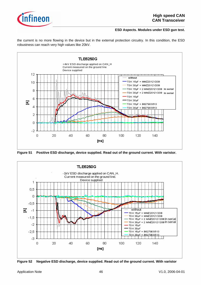
High speed CANCAN Transceiver
ESD Aspects. Modules under ESD gun test.
Application Note 46 V1.0, 2006-04-01
the current is no more flowing in the device but in the external protection circuitry. In this condition, the ESDrobustness can reach very high values like 20kV.
Figure 51 Positive ESD discharge, device supplied. Read out of the ground current. With varistor.
Figure 52 Negative ESD discharge, device supplied. Read out of the ground current. With varistor
without
In serial
In serial
+4kV ESD discharge applied on CAN_HCurrent measured on the ground lineDevice supplied
-1kV ESD discharge applied on CAN_H.Current measured on the ground line.
Device supplied
without
In serialIn serial

Application Note 47 V1.0, 2006-04-01
High speed CANCAN Transceiver
ESD Aspects. PCB layout.
6.4 PCB layout.Knowing all this, and applying the good protection corresponding to the ESD requirement of the application, it isnot given to pass successfully the ESD test. We saw in the Chapter 6.3 that the ESD current is flowing in theground of the device (or in the ground of the external protection). But the ground of the device can be somethingelse than the ground of the module. To equal the two grounds, the PCB layout has to be designed with care.The Figure 53 shows the typical case where the ESD discharge is becoming an issue for the module.
Figure 53 Bad PCB example for ESD.
In the case of the ESD discharge on CAN_H or CAN_L pin, if the ground connector is situated far from thetransceiver, and with digital components as microcontroller in between, the ground line resistance cannot beneglicted. The resultance is an overvoltage, locally on the ground pin of the micro controller, and it can be easilydestroyed !The Figure 54 shows the proper PCB design to avoid these issues. The ground connector has to be as close aspossible to the transceiver.
6.5 Conclusion.For the application targeting to have a good ESD robustness, layout of the board is very important. Providingexternal ESD protection described in Chapter 6.3.3 can allow even more robust design. As the external protectionis influencing the terminations concept, it is also necessary to check the Chapter 5 to comply the busrequirements. In case of varistor usage, a choke coil or at least two coils are necessary. It´s tempting to reducethe varistor threshold voltage. This will improve the ESD robustness of course, but the EMI (Chapter 7) results willbe definitly jeopardized.
TLE6250GTLE6251G / DS
VI
GND
CANH
CANL
7
6
GND
µPTxD
RxD
VCCGND
2
VQ
e.g. TLE 4270
5V
GND
V Drop

High speed CANCAN Transceiver
ESD Aspects. Conclusion.
Application Note 48 V1.0, 2006-04-01
Figure 54 Good PCB design for ESD robustness
TLE6250GTLE6251G / DS
VI
GND
CANH
CANL
7
6
GND
µPTxD
RxD
VCCGND
2
VQ
e.g. TLE 4270
5V
GND
Vs

Application Note 49 V1.0, 2006-04-01
High speed CANCAN Transceiver
EMC aspect. EM Immunity against transcients.
7 EMC aspect.The Electro-Magnetic-Compatibility is a challenge to achieve with CAN applications. Main reason is the wiringharness of the CAN system running into the complete vehicle. The chance to encounter interferences, or to createinterferences in the neighbor of the cables is very high without any design care. In EMC, two domains areconsidered, immunity (EMI) and emission (EME).
7.1 EM Immunity against transcients.The transcients that the transceivers are facing are mainly defined in the international standard ISO 7637 part 1and 2. It consists on checking whether the device is still running properly, or withstand the disturbances and goesback to normal operation afterwards, or might be destroyed. The behavior requested is up to the OEM. The ISOpulses 1, 2 and 3 are representing the disconnection of an inductive load in the wiring harness.
7.2 EM Immunity against RF disturbances.The RF disturbances can be tested by several means. They are described in the ISO11452.
7.2.1 The Stripline test. ISO 11452-5.The stripline test provides a uniform transverse electromagnetic field with the electric field across the strips andthe magnetic field parallel to them. Parallel-plate or co-planar lines are used with the lower plate bounded to theshielded enclosure in which the test takes place. Such lines allow units to be subjected to plane waves over a widefrequency range, and with high field strengths.
7.2.2 The Bulk Current Injection test. (BCI). ISO 11452-4.Bulk Current Injection (BCI) is a test technique pioneered in the aircraft industry which uses current probes (bothpick-up and injection) to couple a 50Ω test and measurement system to a conductor or bundle of conductors suchas a vehicle wiring harness. The probes themselves are RF transformers. An injection probe is driven from theoutput of an RF amplifier and couples the current into the harness of the equipment under test by acting as theprimary of a transformer - the single turn of the harness acting as the secondary. Pick-up probes act in a similarway but this time allow the bulk current in a harness to be monitored using a power meter.
7.3 Infineon transceivers in the EMI disturbances.
7.3.1 Immunity against transcients.The device design is optimized to withstand the ISO pulses. To check it, all devices are checked by anindependant laboratory, the IBEE. They do apply two tests, the damage and the malfunction test.
7.3.1.1 Damage test.Purpose of the damage test is to check whether or not the device withstands the ISO pulses, without anydestruction. The levels of voltage applied are indicated in the Table 4. All infineon high speed transceiverswithstand the distrubances, without destruction.Table 4 Damage testTest pulse Vs max (V) Pulse repetition
frequency (Hz)Test duration (mn) Remarks
1 -100 2 10 t2 = 0s2a +100 2 10 t2 = 0s3a -150 10 103b +150 10 10

High speed CANCAN Transceiver
EMC aspect. Infineon transceivers in the EMI disturbances.
Application Note 50 V1.0, 2006-04-01
7.3.1.2 Malfunction test.During the malfunction test the voltage is increased, for each pulses, until the device is definitively broken. The reached values can be given, on request.
7.3.2 Immunity against RF disturbances.The TEM cell, as well as the BCI tests, are tests at module’s level. The results are stongly dependant on theapplication. It would be possible to test the device in these condition, but the interpretation of the device robustnesswould be impossible, since there’s as much set-up as there are applications. To avoid this and to get theinformation on the RF disturbances robustness, the Direct Power Injection (DPI) test is implemented.
7.3.2.1 BCI test limitationThe Figure 55 shows the typical case of the limitation of BCI, for component test. The transceiver is alone on theboard (for component test). The current probe is injecting 200mA for example. In that case, and assuming thedevice is recessive or OFF, so having an impedance of 30kΩ as a minimum, the voltage on the pins CAN_H andCAN_L will reach 100mA x 30kΩ = 3000 V theoretical (In practice the ESD diode is turning ON). The question isno more to know if the device will be perturbated, but to know if it can overcome the test ! As soon as a capacitoris present, this computation isn´t relevant anymore. But then, it´s no more component test but a test at module’slevel.
Figure 55 BCI test limitation example
7.3.2.2 Principle of the DPI test.The DPI test is, from a principle point of view, similar to the BCI test. The principle is to inject a certain AC voltage,modulated or not, and to check the integrity of the signal (via the RxD pin or the NERR pin of the transceiver). Thetest set up consists of 3 identical transceivers, soldered on a defined PCB. CAN bus is traced on the PCB. Insteadof a current injection, the power is injected via a capacitor (C5 and C6 on Figure 56), and measured in dBm, orWatt. As for the BCI, the power injected is monitored to check the possible reflexions on the bus. One of the mainbenefit of the DPI method is to allow comparison between different supplier’s design on an identical test bench,via a consortium as the ICT for example.
Test PCB
RF currentgenerator
200mA
Termination

Application Note 51 V1.0, 2006-04-01
High speed CANCAN Transceiver
EMC aspect. Infineon transceivers in the EMI disturbances.
Figure 56 DPI test set up
From the DPI results, the BCI and TEM cell result can be easily assessed. The DPI shows the results we can reachwith a perfect module design, on BCI and TEM cell.
7.3.2.3 Results of Infineon’s transceiver under DPI test.The results can be given on request. The Figure 57 shows a typical DPI result curve on the well knownTLE6250G. Others transceivers are available on request. On the X axis, we can find the frequency range. On theY left axe, we can find the maximum power injected without failure. An ideal transceiver would have a straightcurve, so 36dBm injected without any failure. On the Y right axe, we can find the voltage in Volt RMS of the powerinjected, reflecting the reflexions of the line.
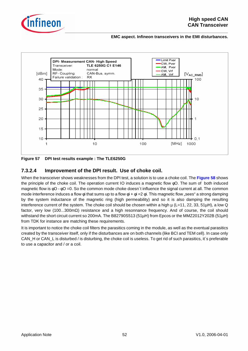
High speed CANCAN Transceiver
EMC aspect. Infineon transceivers in the EMI disturbances.
Application Note 52 V1.0, 2006-04-01
Figure 57 DPI test results example : The TLE6250G
7.3.2.4 Improvement of the DPI result. Use of choke coil.When the transceiver shows weaknesses from the DPI test, a solution is to use a choke coil. The Figure 58 showsthe principle of the choke coil. The operation current ΙO induces a magnetic flow φO. The sum of both inducedmagnetic flow is φO - φO =0. So the common mode choke doesn´t influence the signal current at all. The commonmode interference induces a flow φi that sums up to a flow φi + φi =2 φi. This magnetic flow „sees“ a strong dampingby the system inductance of the magnetic ring (high permeability) and so it is also damping the resultinginterference current of the system. The choke coil should be chosen within a high µ (L=11, 22, 33, 51µH), a low Qfactor, very low (100...300mΩ) resistance and a high resonnance frequency. And of course, the coil shouldwithstand the short circuit current so 200mA. The B82790S513 (51µH) from Epcos or the MMZ2012Y202B (51µH)from TDK for instance are matching these requirements.It is important to notice the choke coil filters the parasitics coming in the module, as well as the eventual parasiticscreated by the transceiver itself, only if the disturbances are on both channels (like BCI and TEM cell). In case onlyCAN_H or CAN_L is disturbed / is disturbing, the choke coil is useless. To get rid of such parasitics, it´s preferableto use a capacitor and / or a coil.

Application Note 53 V1.0, 2006-04-01
High speed CANCAN Transceiver
EMC aspect. Infineon transceivers in the EMI disturbances.
Figure 58 Choke coil principle
The Figure 59 shows the results, witht the same set up as on the Figure 57, adding a chock coil, suppressing thetraditionnal weakness at low frequency.
Figure 59 DPI test results with choke coil for the TLE6250G.
7.3.3 EmissionAs well as for the immunity test, the emission can be performed on the same test bench as for the DPI method.To get emission, it is necessary the transceiver is emitting. The ICT has stated two test pulses. The first one is asquare wave of 250kHz matching an high baudrate application. The second test signal is a 90% duty cycle, at afrequency of 50kHz, matching a low baudrate application. The Figure 60 shows the results of the TLE6250Gunder these conditions. The disturbances are measured on the Y axe in dBµV, the X axe is showing the frequency.
IO
IO = operation currentφO = magnetic flow
Ii = interference currentφi = magnetic flow
Ii
RLOAD
U Operation
U interference
φO
φO
φi
φi

High speed CANCAN Transceiver
EMC aspect. Infineon transceivers in the EMI disturbances.
Application Note 54 V1.0, 2006-04-01
Figure 60 EME test results with TLE6250G, without chock coil
As well as for the immunity, a choke coil can be used. The Figure 61 shows the benefit of the chock coil for thetest signal 1 (square wave of 250kHz). At least 10dBµV reduction can be observed.
Figure 61 EME test results with TLE6250G with and without chock coil
Application Note 55 V1.0, 2006-04-01
High speed CANCAN Transceiver
EMC aspect. Conclusion.
7.4 Conclusion.As well as for the ESD, the EMC performance of the application is strongly dependant on the design care. It isrecommended to plan a choke coil, even if the EMC module test shows good results without. All Infineon’stransceiver are tested according to the method described in this chapter and the reports for each particular partsare available on request. Similar to the comparison between the component test and the module test, the resultof car test is difficult to predict.

High speed CANCAN Transceiver
Products summary
Application Note 56 V1.0, 2006-04-01
8 Products summary
Functionality TLE6250G TLE6250GV33 TLE6251DS TLE6251G Unit commentsVcc supply [4,5;5,5] [4,5;5,5] [4,75;5,25] [4,75;5,25] VVio no [3.0 ;5,5] no [3.0 ; 5,25] VVs no no no [5 ; 40] VEnable Yes Yes Yes YesBus wake up No No Yes YesBus bias in unpowered mode
GND GND weak GND weak GND
SPLIT pin no no Yes YesESD 6 6 6 6 (+/-) kVINH output no no no YesBus time out no no yes yes
Abbreviation Meaning CommentBCI Bulk Current InjectionCAN Controller Area NetworkCDM Charged Device Model ESD testDPI Direct Power Injection EMC testDUT Device Under TestEMC Electro-magnetic CompatibilityEME Electro-magnetic EmissionEMI Electro-magnetic ImmunityEOS Electrical Over StressESD Electro Static DischargeHBM Human Body modelHS CAN High Speed CAN transceiverIBEE IngenieurBurö für industrielle Electrotechnik / ElectronikICT International Conformance and TestingIEC International Electrotechnical CommisionINH InhibitISO International Standard OrganizationLDO Low Drop Output Other name for Voltage regulatorMM Machine Model ESD testOEM Original Equipement Manufacturer In the frame of this document, it means
car makerSC Short CircuitSPT Smart Power Technology Bipolar CMOS and DMOS technology
developped by Infineon

Application Note 57 V1.0, 2006-04-01
High speed CANCAN Transceiver
References.
9 References.[1] Data Sheet High speed CAN, TLE6250G Infineon Technologies AG - Version 3.8
[2] Data Sheet High speed CAN, TLE6251DS Infineon Technologies AG - Version 3.0
[3] Data Sheet High speed CAN, TLE6251G Infineon Technologies AG - version 3.1
[4] Data Sheet, TLE4278G Infineon Technologies AG - version
[5] International Standard ISO 11898-2, Road Vehicles - Controller Area Network (CAN) part 2 High speed medium access unit.
[6] International Standard ISO 11898-5, Road Vehicles - Controller Area Network (CAN) part 5 High speed medium access unit.
[7] Data Sheet, Voltage regulator TLE4275G Infineon Technologies AG version 1.4
[8] Data Sheet, Voltage regulator TLE7270G Infineon Technologies AG version 0.21
[9] Data Sheet, Voltage regulator TLE4266-2G Infineon Technologies AG version 1.2

Published by Infineon Technologies AG
w w w . i n f i n e o n . c o m