High Frequency High-Efficiency Voltage Regulators for ...
232
High Frequency High-Efficiency Voltage Regulators for Future Microprocessors By Jia Wei Dissertation submitted to the faculty of the Virginia Polytechnic Institute and State University in partial fulfillment of the requirements for the degree of Doctor of Philosophy in Electrical Engineering APPROVED Fred C. Lee, Chairman Daan Van Wyk Dushan Borojevic Guo Quan Lu Yilu Liu September 15, 2004 Blacksburg, Virginia Keywords: Voltage Regulator, High Efficiency, High Frequency
Transcript of High Frequency High-Efficiency Voltage Regulators for ...
High Frequency High-Efficiency Voltage Regulators for
Future Microprocessors
By
Jia Wei
Dissertation submitted to the faculty of the
Virginia Polytechnic Institute and State University
in partial fulfillment of the requirements for the degree of
Doctor of Philosophy
in
Electrical Engineering
APPROVED
Fred C. Lee, Chairman
Daan Van Wyk Dushan Borojevic
Guo Quan Lu Yilu Liu
September 15, 2004
Blacksburg, Virginia
Keywords: Voltage Regulator, High Efficiency, High Frequency

High Frequency High-Efficiency Voltage Regulators for
Future Microprocessors
By
Jia Wei
Dr. Fred C. Lee, Chairman
Electrical Engineering
(ABSTRACT)
Microprocessors in today’s computers continue to get faster and more powerful. From
the Intel 80X86 series to today’s Pentium IV, CPUs have greatly improved in
performance. Accordingly, their power consumption has increased dramatically [1][2].
An evolution began in power loss reduction when the high-performance Pentium
processor was driven by a non-standard, less-than-5V power supply, instead of drawing
its power from the 5V plane on the system board. In order to provide the power as
quickly as possible, the voltage regulator (VR), a dedicated DC-DC converter, is placed
in close proximity to power the processor. At first, VRs drew power from the 5V output
of the silver box. As the power delivered through the VR increased so dramatically, it
became no longer efficient to use the 5V bus. Then for desktop and workstation
applications, the VR input voltage moved to the 12V output of the silver box. For laptop
application, the VR input voltage range covers the battery voltage range and the adaptor
voltage. In the meantime, microprocessors will run at very low voltage (sub 1V), and will
consume up to 150A of current, and will have dynamics of about 400A/us.
The current VR solution is the 12V-input multiphase interleaved buck converter. The
switching frequency is around 300KHz. This approach has several limitations for the
future. OSCON capacitor is one limitation due to its large ESR and ESL; the low
switching frequency the second limitation and the large inductance is the third limitation.
Analysis shows that the all-ceramic solution is a better solution than the OSCON solution
when the VR switching frequency reaches 1MHz. However, the 12V-input multiphase
buck converter suffers low efficiency at high switching frequency, which rules out a
legitimate chance of the current VR topology benefiting from high switching frequency.
iii
The extreme duty cycle is the fundamental reason why the 12V-input multiphase
buck converter is not suitable for future VRs. Employing the transformer concept can
extend duty cycle, and therefore offer an opportunity to improve efficiency. The push-
pull buck (PPB) converter is proposed as a solution. The efficiency is improved
compared with the buck converter. Integrated magnetic techniques can be used to further
improve the efficiency and simplify the implementation. The impact of transformer
concept on transient response is analyzed.
The PPB converter efficiency is still not satisfactory at 1MHz due to the switching
loss. Switching loss being a barrier, soft switching is needed. The proposed soft-switched
phase-shift buck (PSB) converter achieves soft switching for the top switches. Highly
efficient power conversion is achieved at high switching frequency. The integrated
magnetics makes the implementation concise and delivers good performance. Given that
the PSB converter has good performance, the matrix-transformer phase-shift buck
(MTPSB) converter is a simplified version of the four-phase PSB converter. The MTPSB
converter trades off some performance with circuit complexity. This feature establishes
itself as a very cost-effective solution for future VRs. The magnetic structure of the
MTPSB converter is also very simple with the use of integrated magnetics.
Mobile CPUs are used in laptop computers. They require very challenging power
management. The challenges for a laptop VR are different from and greater than those for
a desktop VR. A laptop VR needs to have high efficiency at both heavy load and light
load, good transient response and small and light form-factor, and work well with the
wide input voltage range. Future mobile CPUs demand very aggresive power. The
current single-stage VR approach cannot provide a suitable solution for the future. The
PSB converter has disadvantages in light-load efficiency and does not work well with
wide input voltage range; therefore it is not a suitable solution for laptop VRs although it
is still a suitable solution for desktop VRs. The two-stage approach solves the wide-input-
voltage-range issue and improves efficiency at heavy load significantly. The intermediate
bus voltage Vbus is a very important parameter impacting overall efficiency. There is not
one optimal Vbus value for all load conditions. The heavier the load, the higher the
optimal Vbus. Based on this fact, the ABVP control is proposed. Vbus is adaptively
positioned according to the load current therefore optimal Vbus is achieved under most

iv
conditions. Experimental results verify the theoretical prediction. The ONP control is
another control scheme proposed to improve the light-load efficiency. By selecting
optimal number of phases based on mobile processor power states, the VR light-load
efficiency is improved. Experimental results show the proof. The baby-buck concept is
the third concept proposed to improve the very-light-load efficiency. By operating the
baby-buck channel, the two-stage VR improves efficiency at very light load. The two-
stage VR featuring the three proposed control schemes has much higher efficiency than
the single-stage VR over a very wide load range; therefore the battery life is extended.
The two-stage VR with the proposed control schemes is a good solution for future laptop
VRs.
The problem solving process in this work proves that good solutions in isolated
converters can be modified to fit into the non-isolated application. Non-isolated
converters and isolated converters are not two separated worlds. On the contrary, these
two worlds have many things in common. Good concepts can be transplanted from one
world to another with minor modification and many problems can be solved this way.
Another proven point in this work is that sometimes the solution is a fundamental, such
as the change of power delivery architecture. One should not be limited by what is
available right now, and should think outside the box. Once a fundamental change is
made, it is very beneficial to take full advantage of the change, as it provides new
opportunities.

v
Acknowledgements
With sincere appreciation in my heart, I would like to thank my advisor, Dr. Fred C.
Lee for his guidance, encouragement and support throughout this work and my studies
here at Virginia Tech. He changed the direction of my life. I began to know of his great
reputation a long time ago when I was a child. I admired him so much that he was the
reason I chose this path when I started my undergraduate study, back to year 1993. I was
even luckier to have the opportunity to pursue my graduate study as his student here at
the Center for Power Electronics Systems (CPES), one of the best research centers in
power electronics. In the past years, I have learned from him not only power electronics
but also the methods for being a good and successful researcher. This knowledge is going
to benefit me for the rest of my life.
I would also like to thank the other four members of my advisory committee, Dr.
Dusan Borojevic, Dr. Daan Van Wyk, Dr. Guo Quan Lu, and Dr. Yilu Liu, for their
support, suggestions and encouragement. They taught me a great deal about power
electronics and helped me tremendously through my study at CPES.
I was very fortunate to be able to associate with the incredible faculty, staff and
students of CPES. I will cherish the friendships that I have made during my stay here.
Special thanks are due to my fellow students and visiting scholars for their help and
guidance: Dr. Wilson X. Zhou, Dr. Budong You, Dr. Ray-Lee Lin, Dr. Jingdong Zhang,
Dr. Fengfeng Tao, Dr. Yong Li, Dr. Peter Barbosa, Dr. Francisco Canales, Mr. Eric
Baker, Mr. Dengming Peng, Dr. Qun Zhao, Dr. Wei Dong, Mr. Nick Sun, Dr. Zhengxue
Xu, Dr. Bo Yang, Mr. Jia Wu, Mr. Jianwen Shao, Dr. Xiaogang Feng, Dr. Weiyun Chen,
Dr. Xiaochuan Jia, Dr. Zhenxian Liang, Dr. Jinjun Liu, Ms. Qiaoqiao Wu, Mr.
Changrong Liu, Dr. Linyin Zhao, Mr. Roger Chen, Ms. Jinghong Guo Mr. Erik Hertz,
Mr. Sergio Busquets-Monge and Mr. Bin Zhang. I would also like to thank the wonderful
members of the CPES staff who were always willing to help me out, Ms. Teresa Shaw,
Ms. Linda Gallagher, Ms. Teresa Rose, Ms. Ann Craig, Ms. Lesli Farmer, Ms. Marianne
Hawthorne, Ms. Elizabeth Tranter, Ms. Michelle Czamanske, Ms. Linda Long, Mr. Steve
Chen, Mr. Robert Martin, Mr. Jamie Evans, Mr. Dan Huff, Mr. Gary Kerr, Mr. Mike

vi
King, Mr. David Crow, Mr. Joe Price-O’Brien, Mr. Rolando Burgos, and Mr. David
Fuller.
It has been a great pleasure to work with the talented, creative, helpful and dedicated
colleagues from the VRM group. I would like to thank Dr. Peng Xu and Dr. Ming Xu for
being exceptional team leaders who are always willing to go the extra mile to make sure
everything goes well. I would also like to thank all the members of my team: Dr. Pit-
Leong Wong, Dr. Gary Yao, Mr. Mao Ye, Mr. Yu Meng, Mr. Yuancheng Ren, Mr.
Jinghai Zhou, Mr. Yang Qiu, Mr. Shuo Wang, Mr. Liyu Yang, Mr. Kisun Lee, Ms.
Juanjuan Sun, Mr. Doug Sterk, Mr. Ching-Shan Leu, Mr. Julu Sun and Mr. Zhenjian
Liang. It was a real honor working with you guys.
There are some people outside CPES who have made a difference in my life. You
may never realize how much your existence means to me. Without you, I doubt if I could
hang in there and get through all the pain and darkness. Life is so wonderful with you
around! I can’t list all your names but you know who you are.
Finally, my deepest and heartfelt appreciation goes to my family for their
unconditional love. My dad’s unfortunate passing has left a great hole in the hearts of all
my family. It was a very difficult decision for me to come to the U.S. to pursue my
graduate study soon after that. My mum is the greatest mum in the world! She
encouraged me to go for it because she knew that learning power electronics at CPES had
been my dream since I was a kid and that I shouldn’t give it up for any reason. Now I
have made it. Mum and Dad, this dissertation is for you! I would also like to thank my
sister Ms. Jie Wei, and my brother-in-law, Mr. Yuyong Li for their advice and
encouragement during all my frustration. I am so lucky to have you as my family. My
lovely wife Yun He is a very very special person in my life. She is the most wonderful
thing that has ever happened to me. Nothing compares to you! Honey, I love you so
much!
This work was supported by the VRM consortium (Delta Electronics, Hipro
Electronics, Hitachi, Infineon, Intel, Intersil, Linear Technology, National
Semiconductor, Power-One, and Texas Instruments) and the ERC program of the
National Science Foundation under award number EEC-9731677.

vii
TABLE OF CONTENT
Chapter 1. Introduction.................................................................................................... 1
1.1. Background............................................................................................................ 1
1.2. Voltage Regulator (VR) Introduction and Dissertation Objectives ...................... 5
1.3. Dissertation Outline............................................................................................. 13
Chapter 2. Limitations of the Current VR Approach................................................. 15
2.1. The Limitation of OSCON Capacitors. ............................................................... 15
2.2. The Limitation of Low Switching Frequency. .................................................... 36
2.3. The Limitation of Large Inductance.................................................................... 45
2.4. Summary.............................................................................................................. 61
Chapter 3. Innovative Topological Approach to Extend Duty Cycle The Push-
Pull Buck (PPB) Converter............................................................................... 63
3.1. Benefits of Extending Duty Cycle....................................................................... 63
3.2. The Proposed Push-Pull Buck (PPB) Converter. ................................................ 70
3.3. Efficiency Improvement with Integrated Magnetics of the PPB Converter........ 79
3.4. Improved Transient Response of the PPB Converter.......................................... 88
3.5. Summary.............................................................................................................. 97
Chapter 4. Innovative Topological Approach to Eliminate Switching Loss The
Phase-Shift Buck (PSB) Converter .................................................................. 98
4.1. The Limitation of the PPB Converter at High Switching Frequency.................. 98
4.2. The Proposed Soft-Switched Phase-Shift Buck (PSB) Converter. ..................... 99
4.3. Simple Integrated-Magnetics and High Efficiency of the PSB Converter........ 113
4.4. The Proposed Matrix-Transformer Phase-shift Buck (MTPSB) Converter...... 118
4.5. Cost Benefit of the MTPSB VR Solution.......................................................... 127
4.6. Summary............................................................................................................ 131
viii
Chapter 5. The Ultimate Architectural Solution for Future VRs The Two-Stage
Approach.......................................................................................................... 132
5.1. The Unique Challenges for Laptop VRs. .......................................................... 132
5.2. The Limitations of the PSB Solution for Laptop VRs. ..................................... 140
5.3. Benefits of the the Two-Stage Approach. ......................................................... 149
5.4. Improving Sleep-State Efficiency By Adjusting the Intermediate Bus Voltage158
5.5. Improving Light-Load Efficiency Through the Proposed Adaptive Bus-Voltage
Positioning (ABVP). ......................................................................................... 171
5.6. Improving Light-Load Efficiency Through the Proposed Optimal Number-of-
Phases (ONP) Control. ...................................................................................... 187
5.7. Improving Very-Light-Load Efficiency Through the Proposed Baby-Buck (BB)
Concept.............................................................................................................. 194
5.8. Cost Benefit of the Two-Stage Approach Featuring ABVP, ONP and BB. ..... 200
5.9. Summary............................................................................................................ 202
Chapter 6. Conclusion .................................................................................................. 204

LIST OF ILLUSTRATIONS
Fig. 1.1. Historical data on the decrease in the Intel microprocessor silicon process..................................... 1
Fig. 1.2. The number of transistors integrated on the CPU die for Intel processors....................................... 1
Fig. 1.3. Historical data on the increase in power for Intel CPUs. ................................................................. 2
Fig. 1.4. An example of CPU power consumption profile. ............................................................................ 3
Fig. 1.5. Historical data on the scaling of CPU core voltage.......................................................................... 4
Fig.1.6. Intel roadmap of the 32-bit CPU load, (a) CPU die voltage and (b) CPU current demands at CPU-
system connector .................................................................................................................................... 5
Fig. 1.7. Power delivery structures: (a) The initial power delivery architecture for CPUs; and (b) the current
power delivery structure for CPUs. ........................................................................................................ 5
Fig. 1.8. 5V-input single-phase buck VR: (a) The schematic, and (b) a product photograph. ....................... 6
Fig. 1.9. 5V-input multiphase buck VR: (a) The schematic; and (b) a product photograph........................... 7
Fig. 1.10. 12V-input multiphase buck VR: (a) The schematic, and (b) a product photograph. ...................... 8
Fig. 1.11. The VR on a desktop motherboard: (a) a Pentium motherboard; (b) a Pentium IV motherboard;
and (c) a conceptual future motherboard. ............................................................................................. 10
Fig. 1.12. A load line example from Intel VR10 spec. ................................................................................. 11
Fig. 1.13. A thermal imaging of the motherboard area around the CPU socket. .......................................... 12
Fig. 2.1. VR output capacitors used on a Pentium-IV desktop computer motherboard................................ 15
Fig. 2.2. Cost breakdown of the buck VR solution....................................................................................... 16
Fig. 2.3. A load line example from Intel VR10 spec. ................................................................................... 17
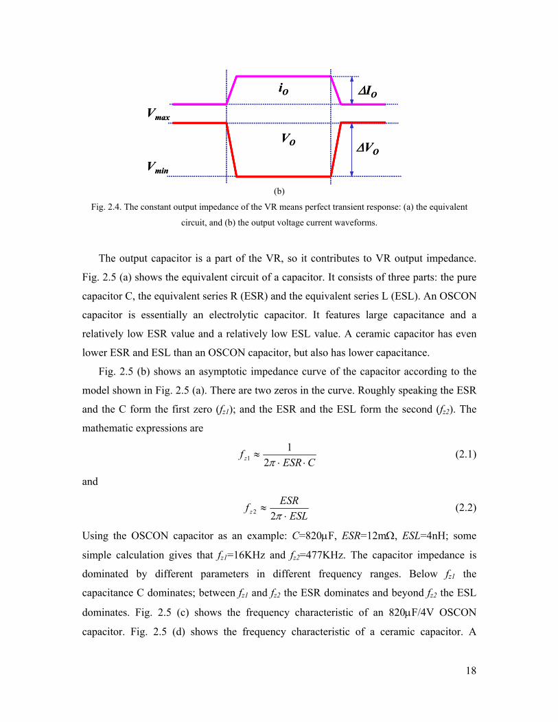
Fig. 2.4. The constant output impedance of the VR means perfect transient response: (a) the equivalent
circuit, and (b) the output voltage current waveforms. ......................................................................... 18
Fig. 2.5. The frequency characteristic of an OSCON capacitor: (a) the capacitor model, (b) the asymptotic
curve of capacitor impedance, (c) the impedance curve of an OSCON capacitor, and (d) the impedance
curve of an OSCON capacitor. ............................................................................................................. 19
Fig. 2.6. VR open loop output impedance: (a) the open-loop buck VR using OSCON capacitors; and (b) the
open-loop output impedance of the VR................................................................................................ 21
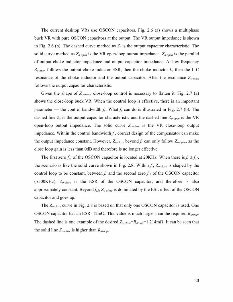
Fig. 2.7. VR close-loop output impedance: (a) the close-loop buck VR using OSCON capacitors; and (b)
the close-loop output impedance of the VR.......................................................................................... 22
Fig. 2.8. Today’s VR close-loop output impedance using one OSCON capacitor. ...................................... 23
Fig. 2.9. Use multiple OSCON capacitors to achieve Rdroop: (a) the output impedance when multiple
OSCON capacitors are paralleled; and (b) a desktop motherboard practice. ....................................... 24
Fig. 2.10. Simulated Zo-close when using all OSCON capacitors. .................................................................. 25
Fig. 2.11. Simulated Vo transient response when using all OSCON capacitors: (a) simplified analysis, and
(b) switching model simulation. ........................................................................................................... 26
x
Fig. 2.12. Creating a new capacitor characteristic by mixing two types of capacitors: (a) OSCON capacitor
characteristic; (b) ceramic capacitor characteristic; and (c) the characteristic by mixing OSCON and
ceramic capacitors. ............................................................................................................................... 28
Fig. 2.13. A simulated Zmix(s) of the mixture of OSCON capacitors and ceramic capacitors....................... 29
Fig. 2.14. Different Zmix(s) created by different amount of ceramic capacitors used: (a) too few ceramic
capacitors; (b) the right amount of ceramic capacitors; and (c) too many ceramic capacitors. ............ 31
Fig. 2.15. Different Zo-close(s) created by different amount of ceramic capacitors used: (a) too few ceramic
capacitors; (b) the right amount of ceramic capacitors; and (c) too many ceramic capacitors. ............ 32
Fig. 2.16. Simulated Zo-close when using all OSCON capacitors. .................................................................. 33
Fig. 2.17. Simulated Vo transient response when using 11 OSCONs plus 300µF ceramic capacitors: (a)
simplified analysis, and (b) switching model simulation...................................................................... 34
Fig. 2.18. Capacitors needed for future VRs. ............................................................................................... 35
Fig. 2.19. Cost estimation for future VRs..................................................................................................... 35
Fig. 2.20. VR open loop output impedance: (a) ceramic capacitor characteristics; (b) the open-loop buck
VR using all-ceramic capacitors; and (c) the close-loop output impedance of the VR. ....................... 37
Fig. 2.21. Ceramic capacitor characteristics and the simulated Zo-close. ........................................................ 38
Fig. 2.22. Simplified VR equivalent circuit and the transient response: (a) VR equivalent circuit; and (b) the
transient response obtained through the equivalent circuit................................................................... 39
Fig. 2.23. The switching model simulation result of Vo transient response. ................................................. 40
Fig. 2.24. Options of VR output capacitors: (a) OSCONs plus ceramics, and (b) the all-ceramic solution.41
Fig. 2.25. Experimental test results of the transient response: (a) OSCONs plus ceramics, (b) the all-
ceramic solution, and (c) the load current step change. ........................................................................ 42
Fig. 2.26. Cost comparison of the OSCON solution and the all-ceramic solution: (a) At 300KHz switching
frequency, and (b) at 1MHz switching frequency. ............................................................................... 44
Fig. 2.27. Efficiency comparison of the 12V-input multiphase buck VR at 300KHz and 1MHz switching
frequency. ............................................................................................................................................. 45
Fig. 2.28. Power delivery architectures for desktop computers: (a) With 5V-input VRs, and (b) with 12V-
input VRs.............................................................................................................................................. 46
Fig. 2.29. Key waveforms in a buck VR when input voltage is 5 V and 12 V: (a) the inductor current, (b)
the top switch current, (c) the phase voltage, and (d) the bottom switch current. ................................ 49
Fig. 2.30. VR loss breakdown with 5V and 12V input voltage. ................................................................... 50
Fig. 2.31. Photograph of the four-phase interleaved buck VR prototype. .................................................... 51
Fig. 2.32. Experimental test waveforms of the buck VR.............................................................................. 51
Fig. 2.33. Efficiency of the four-phase interleaved buck VR. ...................................................................... 52
Fig. 2.34. Key waveforms in a buck VR when input voltage is 5 V and 12 V: (a) the inductor current, (b)
the top switch current, and (c) the bottom switch current..................................................................... 53
Fig. 2.35. VR loss breakdown with 300nH and 500nH inductance.............................................................. 54

xi
Fig. 2.36. Measured efficiency of a buck VR with 300nH and 500nH inductance. ..................................... 54
Fig. 2.37. Inductances smaller than Lct give the same transient responses: The transient voltage spikes
increase for inductances larger than Lct. ............................................................................................... 55
Fig. 2.38. The relationship of inductance L and transient voltage spike ∆Vo: (a) for 5V-input buck VRs, and
(b) for 12V-input VRs. ......................................................................................................................... 57
Fig. 2.39. Inductance impact on transient voltage spikes. ............................................................................ 58
Fig. 2.40. Simulated transient voltage spikes: (a) For 5V-input VRs, and (b) for 12V-input VRs............... 59
Fig. 2.41. Simulated transient voltage spikes with more output capacitors.................................................. 59
Fig. 2.42. Concept of adaptive voltage positioning (AVP): (a) when L < Lct, and (b) when L > Lct............ 61
Fig. 3.1. Extending duty cycle: (a) using transformer concept to extend duty cycle (b) extending duty cycle
reduces top switch turn-off current; and (c) extending duty cycle reduces the phase voltage.............. 65
Fig. 3.2. The tapped-inductor buck converter: (a) the schematic; and (b) the operation principle. .............. 67
Fig. 3.3. Comparison of the duty cycles of buck converter and tapped-inductor buck converter................. 68
Fig. 3.4. Integrated-magnetic implementation of the tapped-inductor buck VR. ......................................... 68
Fig. 3.5. Photograph of the four-phase interleaved tapped-inductor buck VR prototype. ............................ 69
Fig. 3.6. Test waveforms of the tapped-inductor buck VR........................................................................... 69
Fig. 3.7. Measured efficiency of the tapped-inductor buck VR.................................................................... 70
Fig. 3.8. The push-pull converter with current doubler. ............................................................................... 71
Fig. 3.9. The push-pull forward converter with current doubler................................................................... 71
Fig. 3.10. A general concept of direct energy transfer: (a) Conventional connection, and (b) with the direct-
energy-transfer concept. ....................................................................................................................... 73
Fig. 3.11. The proposed push-pull buck (PPB) converter with current doubler. .......................................... 73
Fig. 3.12. The operation principle of the proposed Push-Pull Buck (PPB) converter. ................................. 75
Fig. 3.13. The equivalent circuit of the push-pull buck converter: (a) During t1~t2; (b) during t2~t3; and (c)
during t3~t4............................................................................................................................................ 76
Fig. 3.14. Comparison of the key waveforms of: (a) The PPB and the PPB converters; and (b) the PPB
converter and the buck converters. ....................................................................................................... 78
Fig. 3.15. Loss comparison of the PPB converter and the two-phase buck converter. ................................. 79
Fig. 3.16. Integrated magnetic structure 1 of the push-pull buck converter: (a) The schematic associated
with IM-1 structure, and (b) IM-1 structure. ........................................................................................ 80
Fig. 3.17. Integrated magnetic structure 2 of the push-pull buck converter: (a) The schematic associated
with IM-2 structure; and (b) IM-2 structure. ........................................................................................ 81
Fig. 3.18. Integrated magnetic structure 3 of the push-pull buck converter: (a) The schematic associated
with IM-3 structure, and (b) IM-3 structure. ........................................................................................ 82
Fig. 3.19. Integrated magnetic structure 4 of the push-pull buck converter: (a) The schematic associated
with IM-4 structure; (b) IM-4 structure and (c) the current waveforms. .............................................. 84

xii
Fig. 3.20. IM structure prototypes of the PPB converter: (a) IM-1 structure prototype, (b) IM-2 structure
prototype, (c) IM-3 structure prototype, and (d) IM-4 structure prototype........................................... 87
Fig. 3.21. Experimental test waveforms of the PPB converter. .................................................................... 88
Fig. 3.22. Measured efficiency comparison of the PPB converter and the buck converter. ......................... 88
Fig. 3.23. Deriving the inductor current slew rate of the PPB converter: (a) the original PPB converter, and
(b) the equivalent circuit in deriving the critical inductance. ............................................................... 91
Table 3.1 Lct1 and Lct2 of the buck converter and the PPB converter ............................................................ 92
Fig. 3.24. Lct1 and Lct2 of the PPB converter and the buck converter............................................................ 92
Fig. 3.25. Loss estimation of the buck converter and the PPB converter with different turn’s ratio n. ........ 93
Fig. 3.26. Scenarios created by different turn’s ratio n in the PPB converter: (a) Lct1>Lct2; (b) Lct1=Lct2; and
(c) Lct1<Lct2. .......................................................................................................................................... 95
Fig. 3.27. Choose turn’s ratio n to get the best transient response................................................................ 96
Fig. 3.28. Measured transient response of the buck converter and the PPB converter: (a) The buck converter
and (b) n=2 PPB converter. .................................................................................................................. 96
Fig. 4.1. Efficiency comparison of the PPB converter switching at 300 KHz and 1 MHz........................... 99
Fig. 4.2. Loss analysis of the PPB converter switching at 300 KHz and 1 MHz.......................................... 99
Fig. 4.3. The full-bridge converter with current-doubler output................................................................. 101
Fig. 4.4. Deriving an autotransformer version from the full-bridge converter: (a1) the transformer version,
when Q4 and Q3 are “on”, (a2) the autotransformer version, when Q4 and Q3 are “on”, (b1)the
transformer version, when Q1 and Q2 are “on”, (b2) the autotransformer version, when Q1 and Q2 are
“on”, (c1) the transformer version, when Q1 and Q4 are “on”, (c2) the autotransformer version, when
Q1 and Q4 are “on”, (d1) the transformer version, when Q2 and Q3 are “on”, and (d2) the
autotransformer version, when Q2 and Q3 are “on”........................................................................... 102
Fig. 4.5. The proposed phase-shift buck converter..................................................................................... 104
Fig. 4.6. The operation principle of the proposed phase-shift buck converter............................................ 105
Fig. 4.7. Subintervals of the Circuit Operation: (a) t0~t1, (b) t1~t2, (c) t2~t3, (d) t3~t4, (e) t4~t5, (f) t5~t6, (g)
t6~t7, (h) t7~t8, (i) t8~t9, (j) t9~t0. .......................................................................................................... 109
Fig. 4.8. Loss comparison of the buck converter, the push-pull buck converter, and the phase-shift buck
converter. ............................................................................................................................................ 112
Fig. 4.9. Drivers of the phase-shift buck converter: (a) the conventional bootstrap driver, and (b) the
proposed bootstrap driver. .................................................................................................................. 113
Fig. 4.10. The integrated magnetics structure of the phase-shift buck converter. ...................................... 114
Fig. 4.11. The integrated magnetics structure using PCB windings: (a) the air gaps, and (b) the 3-D view of
the structure when n=1. ...................................................................................................................... 115
Fig. 4.12. The photograph of the phase-shift buck converter prototype. .................................................... 116
Fig. 4.13. The measured efficiency comparison......................................................................................... 116
xiii
Fig. 4.14. Test waveforms of the PSB prototype, (a) ZVS turn-on, (b) Top switch waveforms and (c)
Bottom switch waveforms. ................................................................................................................. 117
Fig. 4.15. The four-phase phase-shift buck converter. ............................................................................... 120
Fig. 4.16. The proposed matrix-transformer phase-shift buck (MTPSB) converter. .................................. 120
Fig. 4.17. The equivalent circuits of the matrix-transformer phase-shift buck converter: (a) when Q1 and
Q2 are both on, and (b) when Q3 and Q4 are both on. ....................................................................... 121
Fig. 4.18. The equivalent PSB of the matrix-transformer phase-shift buck converter. .............................. 121
Fig. 4.19. Loss comparison of the buck converter, the PSB converter, and the MTPSB converter. .......... 122
Fig. 4.20. The integrated magnetics structure of the matrix-transformer phase-shift buck converter: (a)
Following the PSB implementation, (b) the top view, (c) the air gaps, and (d) the 3-D view............ 123
Fig. 4.21. Photograph of the phase-shift buck converter prototype............................................................ 124
Fig. 4.22. The measured efficiency: (a) efficiency comparison of the matrix-transformer phase-shift buck
converter and the four-phase phase-shift buck converter, and (b) efficiency comparison of the matrix-
transformer phase-shift buck converter and the four-phase buck converter. ...................................... 125
Fig. 4.23. Test waveforms of the MTPSB prototype, (a) ZVS turn-on, (b) Top switch waveforms and (c)
Bottom switch waveforms. ................................................................................................................. 126
Fig. 4.24. VR solutions: (a) current desktop computer VR solution, (b) current server VR solution, and (c)
the proposed MTPSB solution............................................................................................................ 129
Fig. 4.25. Cost breakdown of the VR solutions: (a) current desktop computer VR solution, (b) current
server VR solution, and (c) the proposed MTPSB solution................................................................ 130
Fig. 5.1. The PC market as of year 2002. ................................................................................................... 133
Fig. 5.2. The PC market growth: (a) desktop PCs, and (b) mobile PCs. .................................................... 133
Fig. 5.3. Today’s laptop computer power delivery structure. ..................................................................... 133
Fig. 5.4. Today’s laptop VR solution: multiphase buck converter. ............................................................ 134
Fig. 5.5. Historical data on current consumption of Intel mobile microprocessors. ................................... 134
Fig. 5.6. The photograph of the VR solution of IBM Thinkpad A32 laptop computer. ............................. 135
Fig. 5.7. Li-ion battery pack discharge characteristics. .............................................................................. 136
Fig. 5.8. A laptop computer base power consumption analysis.................................................................. 137
Fig. 5.9. The mobile CPU power consumption. ......................................................................................... 137
Table 5.1 Comparisons of Desktop VR and Laptop VR ............................................................................ 139
Fig. 5.10. The single-stage VR power architecture: (a) The PSB solution for desktop VRs; and (b) the PSB
solution for laptop VRs....................................................................................................................... 140
Table 5.2 Evaluation of the PSB Converter as a Desktop VR.................................................................... 141
Fig. 5.11. The PSB solution for laptop VRs. .............................................................................................. 142
Fig. 5.12. Light-load operation of the PSB converter................................................................................. 143
Fig. 5.13. The low efficiency of the PSB converter at light load................................................................ 144
Fig. 5.14. Loss comparison of the buck solution and the PSB solution...................................................... 145
xiv
Table 5.3. Battery Run Time Comparison of the Buck Solution and the PSB Solution............................. 145
Fig. 5.15. The issues caused by the wide duty cycle range of the PSB solution for laptop VR. ................ 146
Table 5.4 Evaluation of the PSB Converter as a Desktop VR and a Laptop VR........................................ 147
Fig. 5.16. The issues caused by the wide duty cycle range of the PSB solution for laptop VR. ................ 148
Fig. 5.17. The issues caused by the wide duty cycle range of the PSB solution for laptop VR. ................ 148
Fig. 5.18. The buck VR has high efficiency at high frequency when the input voltage is low. ................. 149
Fig. 5.19. The proposed two-stage laptop VR. ........................................................................................... 150
Fig. 5.20. How the optimal bus voltage concept comes into the picture: (a) First-stage efficiency, (b)
second-stage efficiency, and (c) overall efficiency............................................................................. 152
Fig. 5.21. The two-stage VR can benefit from low voltage-rating devices: (a) first-stage efficiency, (b)
second-stage efficiency, and (c) overall efficiency............................................................................. 154
Fig. 5.22. The efficiency comparison of the two-stage solution and the single-stage solution: (a) the single-
stage solution, (b) the two-stage solution, (c) the photograph of the two-stage VR prototype, and (d)
the measured efficiency comparison. ................................................................................................. 156
Fig. 5.23. Loss comparison of the buck solution and the two-stage solution. ............................................ 157
Table 5.5. Battery Run Time Comparison of the Buck Solution and the Two-Stage Solution .................. 157
Table 5.6 Evaluation of The Two-Stage Approach for Laptop VRs .......................................................... 158
Fig. 5.24. The load impact on the Vbus that delivers the highest second-stage efficiency: (a1) calculated
efficiency vs. Vbus at 5A output, (b1) measured efficiency vs. Vbus at 5A output, (a2) calculated
efficiency vs. Vbus at 15A output, (b2) measured efficiency vs. Vbus at 15A output, (a3) calculated
efficiency vs. Vbus at 25A output, (b3) measured efficiency vs. Vbus at 25A output............................ 160
Fig. 5.25. How the optimal Vbus forms........................................................................................................ 161
Fig. 5.26. Experimental data showing that the optimal Vbus changes as the load changes.......................... 162
Fig. 5.27. The global system power states and transitions.......................................................................... 163
Fig. 5.28. The proposed adjustable Vbus: (a) The Mobile CPU Power States and the Power Consumption,
and (b) the proposed variable Vbus control scheme based on the ACPI information........................... 165
Fig. 5.29. The implementation of the variable Vbus control scheme based on the ACPI information. ........ 165
Fig. 5.30. Transient response of the variable Vbus control scheme based on the ACPI information: (a) the
simulation result, and (b) the experimental test result. ....................................................................... 166
Fig. 5.31. Simulated Vbus response and Vo response: (a) Vbus response with 3V change in magnitude, and (b)
Vo response showing an obvious glitch............................................................................................... 167
Fig. 5.32. Zoomed-in waveforms of Io step change, Vbus response and Vo response................................... 167
Fig. 5.33. The simulated audio susceptibility of the second stage.............................................................. 168
Fig. 5.34. Adding the feed forward function into the second stage. ........................................................... 169
Fig. 5.35. The simulated audio susceptibility of the second stage with the feed-forward function. ........... 170
Fig. 5.36. The simulated waveforms when the feed forward function is added: (a) the ramp waveform, and
(b) Vo response showing that the glitch is eliminated. ........................................................................ 170

xv
Fig. 5.37. The limitations of the ACPI-based variable Vbus control scheme. .............................................. 172
Fig. 5.38. The ideal positioning of Vbus....................................................................................................... 172
Fig. 5.39. Vbus-Io relationship: (a) A more accurate implementation, and (b) a simpler implementation. .. 173
Fig. 5.40. The proposed adaptive bus-voltage positioning. ........................................................................ 173
Fig. 5.41. The proposed current-injection implementation of ABVP......................................................... 175
Fig. 5.42. Simulation result of the proposed current-injection implementation of ABVP: (a) Vbus response
and (b) Vo response. ............................................................................................................................ 175
Fig. 5.43. Experimental test waveforms of ABVP. .................................................................................... 176
Fig. 5.44. Frequency-domain representations of the ABVP-AVP system: (a) ABVP, and (b) AVP. ........ 177
Fig. 5.45. The zoomed waveforms of the current-injection ABVP-AVP two-stage VR. ........................... 178
Fig. 5.46. The ABVP-AVP response when there is fIo< fc1< fc2. ................................................................ 180
Fig. 5.47. The inductor current waveforms when there is fc1< fc2< fIo: (a) Io, (b) iL1, and (c) iL11............... 181
Fig. 5.48. The ABVP-AVP response when there is fc1< fc2< fIo. ................................................................ 182
Fig. 5.49. The inductor current waveforms when fc1 < fIo< fc2: (a) Io, (b) iL1, (c) iL11, (b) Vbus, and (e) Vo.. 184
Fig. 5.50. Experimental test efficiency: (a) The efficiency of the two-stage VR with and without the ABVP
control, and (b) the efficiency of the two-stage VR with ABVP and the single-stage VR................ 186
Fig. 5.51. Loss comparison of the buck solution, the two-stage solution, and adding ABVP.................... 187
Table 5.7. Battery Run Time Comparison of the Buck Solution, the Two-Stage Solution, and adding ABVP
............................................................................................................................................................ 187
Fig. 5.52. Light-load inefficiency: (a) one phase of the second-stage multiphase buck converter, (b) the gate
drive loss, (c) the top switch loss and (d) the bottom switch loss....................................................... 189
Fig. 5.53. Calculated efficiency with different numbers of 2nd-stage phases. ........................................... 191
Fig. 5.54. Experimental verification of efficiency improvement of the ONP control. ............................... 191
Fig. 5.55. Efficiency improvement from the ONP control: (a) Efficiency of the two-stage VR with ABVP &
ONP control, and (b) efficiency comparison of the two-stage VR and the single–stage VR. ............ 192
Fig. 5.56. Loss comparison of the buck solution, the two-stage solution, adding ABVP, and adding ONP.
............................................................................................................................................................ 193
Table 5.8. Battery Run Time Comparison of the Buck Solution, the Two-Stage Solution, adding ABVP and
adding ONP ........................................................................................................................................ 193
Fig. 5.57. Efficiency of TPS54612 monolithic buck converter. ................................................................. 195
Fig. 5.58. The proposed baby-buck concept............................................................................................... 196
Fig. 5.59. Efficiency of the two-stage VR: (a) The two-stage VR efficiency with and without the baby-buck
concept; and (b) the efficiency comparison between the single stage VR and the two-stage VR
featuring ABVP, ONP and BB concepts. ........................................................................................... 196
Fig. 5.60. Loss comparison of the buck solution, the two-stage solution, adding ABVP, adding ONP, and
adding BB........................................................................................................................................... 197
xvi
Table 5.9. Battery Run Time Comparison of the Buck Solution, the Two-Stage Solution, adding ABVP,
adding ONP, and adding BB .............................................................................................................. 198
Table 5.10. Battery Run Time Comparison at Extremely Light Load........................................................ 199
Table 5.11. Battery Run Time Comparison at Extremely Heavy Load...................................................... 199
Table 5.12. Evaluation of the Two-Stage Approach for Laptop VRs After Implementing ABVP, ONP and
BB Controls ........................................................................................................................................ 200
Fig. 5.61. The single-stage buck solution for laptop VRs. ......................................................................... 201
Fig. 5.62. Efficiency comparison of 250KHz single-stage buck solution and 1MHz two-stage VR solution
featuring ABVP, ONP and BB. .......................................................................................................... 201
Fig. 5.63. Cost comparison of 250KHz single-stage buck solution and 1MHz two-stage VR solution
featuring ABVP, ONP and BB. .......................................................................................................... 202
1
Chapter 1. Introduction
1.1. Background.
CPUs continue to get faster and more powerful. From Intel’s 4004 to today’s Pentium
IV, they have greatly improved their clock frequency by three orders of magnitude
through the continuing scaling of Complementary Metal-Oxide-Silicon (CMOS)
manufacturing technology. Fig. 1.1 shows the historical data on the Intel CPU silicon
process. The data shows that the process is 1.1µm in year 1986 and is down to 0.09µm as
of year 2004. Microprocessor scaling has consistently adhered to Moore’s law [109],
verified by Fig. 1.2, which shows the historical data on the number of transistors
integrated on an Intel CPU die. As the result, Pentium IV CPU die has hundreds of
millions of transistors, as opposed to thousands of transistors on a 4004 CPU die.
0
0.2
0.4
0.6
0.8
1
1.2
Q4'86
Q4'88
Q4'90
Q4'92
Q4'94
Q4'96
Q4'98
Q4'00
Q4'02
Q4'04
CPU
Pro
cess
(µm
)
Fig. 1.1. Historical data on the decrease in the Intel microprocessor silicon process.
Fig. 1.2. The number of transistors integrated on the CPU die for Intel processors.

2
The electrical power consumed by the CPU is given by formula 1.1,
CCCPU VCfAVP 2⋅⋅⋅= (1.1)
where AV is the activity factor, f is the clock frequency, C is the lumped capacitance of
all the logic gates, and VCC is the CPU core voltage. The scaling of CPU increases the
capacitance C. For a fixed die size, with MOS transistor channel length, oxide thickness,
and supply voltage all decreasing by about 0.7x per generation, the total circuit
capacitance C increases by 1.43x (i.e. 1/0.7) [113]. The increase of C combined with the
performance demanded from next-generation microprocessors results in increased
processor power [1][2][3]. Fig. 1.3 shows the historical data on the increase in power for
Intel CPUs [108]. It is observed that as the clock speed scales up over time, so does the
power dissipation of microprocessors.
Fig. 1.3. Historical data on the increase in power for Intel CPUs.
The CPU consumes electrical power and eventually turns it into heat. This poses great
challenges to CPU thermal management. Several efforts have been made to reduce the
heat generated by the CPU.
One method is to improve CPU architecture and design to contain and manage CPU
power against CPU performance as well as die area [107]. Power-saving features in the
CPU architecture mandate various operating conditions that lower power consumption to
a minimum through “sleep,” “stand-by,” “idle,” and “power-down” states. This reduces
AV in formula 1.1. Fig. 1.4 shows an example of CPU power consumption profile [107].
Pmax is the maximum possible CPU power drawn under normal operating conditions. Ptdp

3
is the thermal design power, which is the maximum sustained power across a set of
realistic applications drawn under normal operating conditions. Pactive is the thermal
design power time averaged over a period of time >> thermal time constant. The CPU
performs data processing during App 1, App 2, and App 3 and stays in idle states
thereafter. The idle state power is consumed in quiescent states where there is little or no
clock activity. Examples are the sleep states of CPUs. By entering sleep states, the CPU
average power is effectively reduced.
App1: a high power application
App2: a low power application
App3: a medium power application
Fig. 1.4. An example of CPU power consumption profile.
Another method to reduce the heat generated by the CPU is to scale CPU core voltage
VCC. Fig. 1.5 shows the historical data on the scaling of CPU core voltage. As of year
1999, CPU core voltage had decreased from 5V to less than 2V as CPU clock frequency
increased. Since CPU power consumption is proportional to VCC2, it decreases
significantly as VCC decreases.

4
0
Year19991997199519931991
5
4
3
2
1
Vcc
(V)
i386™Intel® Pentium®
Intel® Pentium® III
Fig. 1.5. Historical data on the scaling of CPU core voltage.
Although the above two methods are effective ways to reduce CPU power
consumption, the power reduction obtained from architecture and process modifications
is not commensurate with the scaling in die size, voltage, and frequency to support a cap
in power consumption; therefore the power consumption of CPUs is still trended higher
for the future [107]. CPU current increases from 10, 20A to 100A range, and is expected
to increase to 150A range in the near future. Fig. 1.6 shows the roadmap of voltage and
current of Intel 32-bit CPUs [1]. Fig. 1.6 (a) shows that future CPUs will run at sub 1V
with an ever-tighter voltage tolerance. Meanwhile, Fig.1.6 (b) indicates a high current
consumption reaching over 100A, and fast dynamics of about 400A/us.
5
2.2
2.0
1.8
1.6
1.4
1.2
1.0
0.8
1999 2000 2001 2002 2003 2004 2005Year
Vcc
(V)
Vcc set pointMax. Tol.Min. Tol.
CPU Die Voltage
140
120
100
80
60
40
20
01999 2000 2001 2002 2003 2004
Year
Icc
(A)
Iccdi/dt
CPU Current Demands450400350300250200150100500
2005
di/d
t (A
/us)
(a) (b)
Fig.1.6. Intel roadmap of the 32-bit CPU load, (a) CPU die voltage and (b) CPU current demands at CPU-system connector
1.2. Voltage Regulator (VR) Introduction and Dissertation Objectives
Fig. 1.7 (a) shows the initial power delivery architecture for CPU. The CPU draws
power form the 5V output of the silver box directly. The scaling of CPU core voltage VCC
leads to a change of the power delivery architecture. As the high-performance Pentium
CPU demands a non-standard, less-than-5V power supply, the voltage regulator (VR), a
dedicated DC-DC converter, is placed in close proximity to power the CPU. Fig. 1.7 (b)
shows the current power delivery architecture for CPUs. A voltage regulator converts the
silver box output voltage to a suitable regulated DC voltage rail to power the core of the
CPU.
Silver BoxVcc=5VAC
CPUCPU
(a)
Silver Box5V/12VAC
VRVcc<5V
CPUCPU
(b)
Fig. 1.7. Power delivery structures: (a) The initial power delivery architecture for CPUs; and (b) the
current power delivery structure for CPUs.
6
At first, the VR draws power from the 5V output of the silver box. The topology is
the single-phase buck converter, as shown in Fig. 1.8 (a). Fig. 1.8 (b) shows the
photograph of a VR product of that time. The output voltage is 2V and the output current
is 13A.
Co RL5V Q2Q1
L
(a)
(b)
Fig. 1.8. 5V-input single-phase buck VR: (a) The schematic, and (b) a product photograph.
As CPU power increases, a single-phase buck converter can no longer deliver the
required current. Handling the high current in a single-phase converter would place high
thermal demands on the components in the system such as the inductors and MOSFETs
(metal-oxide semiconductor field-effect transistors). Therefore the VR topology adopts
the multiphase buck converter [4][5][6][7][8][9][10][12], as shown in Fig. 1.9 (a),
proposed by VPEC/CPES in 1997. Fig. 1.9 (b) shows the photograph of a VR product
from ON Semiconductor in year 1999. It is a two-phase buck converter. The input
voltage is 5V, the output voltage is 1.7V, and the output current is 35A. Multiphase
operation is important for producing the high currents and low voltages demanded by
today’s CPUs, as it reduces current ripple by interleaving phases and provides better
thermal management due to the distributed structure. However, using more phases not
only increases cost, but overall complexity as well.

7
Co RL5VQ2Q1
Q4Q3
L
L
(a)
(b)
Fig. 1.9. 5V-input multiphase buck VR: (a) The schematic; and (b) a product photograph..
As the power delivered through the VR increases dramatically, the power of the 5V
output of the silver box is so high that the distribution loss on the 5V bus is quite
considerable. Hooking the VR to the 5V bus is no longer efficient from the system point
of view; therefore, VR input voltage moves to the 12V output of the silver box. In the
meantime, more phases are used because higher current is delivered through the VR. Fig.
1.10 (a) shows the state-of-the-art VR topology the 12V-input multiphase buck
converter. Fig. 1.10 (b) shows the photograph of a VR product from Intersil Corporation.
It is a four-phase buck converter. The input voltage is 12V, the output voltage is 1.45V,
and the output current is 60A.
8
Co RL12VQ2Q1
Q4Q3
Q6Q5
Q8Q7
L
L
L
L
(a)
IntersilIntersil
(b)
Fig. 1.10. 12V-input multiphase buck VR: (a) The schematic, and (b) a product photograph.
Decreasing the size is one of the great challenges for designing VRs. As VRs evolve,
they require more motherboard space. Fig. 1.11 (a) shows a photograph of a Pentium
computer motherboard. The marked rectangular area is the VR powering a CPU
demanding approximately 10A current. It accounts for only 2% of the motherboard space.
Fig. 1.11 (b) shows the photograph of a Pentium IV motherboard. The marked
rectangular area is the VR powering a CPU demanding 60 ~ 70A current. It accounts for
12% of the motherboard space. Comparing Fig. 1.11 (a) and (b), it can be observed that
the VR size increases by five times as the VR out current increases by five times. In other
words, the power density of the VRs is the same. Fig. 1.11 (c) shows a conceptual
motherboard for future CPUs demanding 150A current and sub 1V voltage if the present
approach still applies. Approximately 30% of the motherboard area is for the VR. This is
a very questionable approach because the motherboard cannot afford so much precious
space for the VR.

9
(a)
(b)

10
(c)
Fig. 1.11. The VR on a desktop motherboard: (a) a Pentium motherboard; (b) a Pentium IV
motherboard; and (c) a conceptual future motherboard.
A stringent transient response requirement is also one of the great challenges for the
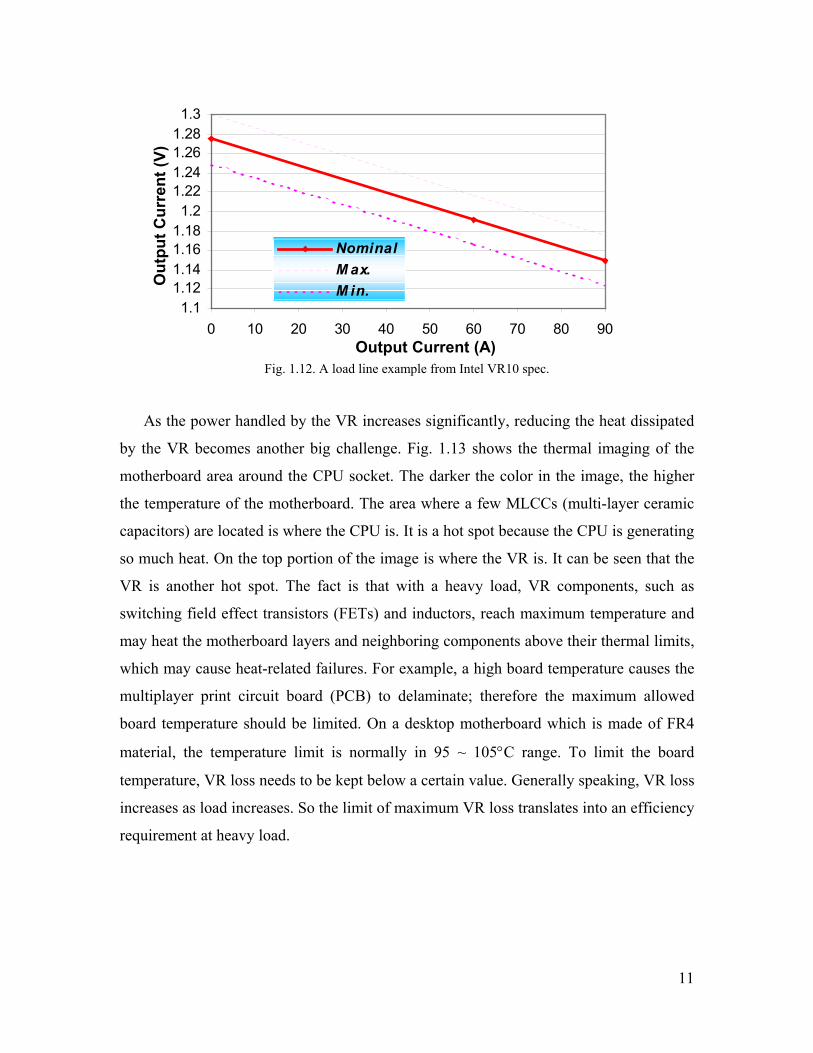
design of VRs. Fig. 1.12 shows a VR load line example from Intel VR 10 spec. The
vertical axis is the VR output voltage and the horizontal axis is the VR output current.
The solid line is the nominal load line and the dotted lines describe the regulation band.
The VR output voltage needs to be positioned according to load current, and needs to stay
within the stringent regulation band. However, in a CPU, the high clock speed circuits
and power conservation design techniques such as clock gating and sleep modes result in
fast, unpredictable, and large magnitude changes in the supply current. Fig. 1.6 (b) and
[1][2][3] have shown this trend. The rate of change could be many Amps per nanosecond.
If not well managed, these current transients may cause the VR output voltage to go
outside the regulation band and manifest them as power supply noise that ultimately
limits how fast the CPU can operate. This is further compounded by the reduced noise
margin in the CMOS logic circuits that result from power supply voltage scaling. While
voltage overshoots may cause the CPU reliability to degrade, undershoots may cause
malfunctions of the CPU, often resulting in the “blue screen”.
11
1.11.121.141.161.181.2
1.221.241.261.281.3
0 10 20 30 40 50 60 70 80 90
NominalM ax.M in.
Output Current (A)
Out
put C
urre
nt (V
)
Fig. 1.12. A load line example from Intel VR10 spec.
As the power handled by the VR increases significantly, reducing the heat dissipated
by the VR becomes another big challenge. Fig. 1.13 shows the thermal imaging of the
motherboard area around the CPU socket. The darker the color in the image, the higher
the temperature of the motherboard. The area where a few MLCCs (multi-layer ceramic
capacitors) are located is where the CPU is. It is a hot spot because the CPU is generating
so much heat. On the top portion of the image is where the VR is. It can be seen that the
VR is another hot spot. The fact is that with a heavy load, VR components, such as
switching field effect transistors (FETs) and inductors, reach maximum temperature and
may heat the motherboard layers and neighboring components above their thermal limits,
which may cause heat-related failures. For example, a high board temperature causes the
multiplayer print circuit board (PCB) to delaminate; therefore the maximum allowed
board temperature should be limited. On a desktop motherboard which is made of FR4
material, the temperature limit is normally in 95 ~ 105°C range. To limit the board
temperature, VR loss needs to be kept below a certain value. Generally speaking, VR loss
increases as load increases. So the limit of maximum VR loss translates into an efficiency
requirement at heavy load.

12
Fig. 1.13. A thermal imaging of the motherboard area around the CPU socket.
The two most common types of personal computer (PC) are desktop computers and
laptop computers. Laptop VRs encounter all the technical challenges that desktop VRs do,
and more due to their special work conditions. One unique challenge is how to prolong
battery life. Battery life is calculated based on formula (1.2),
Battery Life (hr)=
Input Power Capacity (Whr)Average Platform Power Consumption
(1.2)
in which VR efficiency has a significant impact on average platform power consumption.
Since the CPU is very frequently in sleep states, the VR is frequently at light-load
conditions. High efficiency at light load is more important than ever for a laptop VR. It is
desirable to achieve high efficiency in the entire load range. Another unique challenge for
laptop VRs is how to maintain high efficiency with the wide input voltage range. Laptop
VRs need to work with battery packs and adapters, and thus need to work with a wide
input voltage range. This wide input voltage makes it difficult for the VR to maintain
high efficiency.
The preceding discussion has explained the main challenges of VRs. They include the
need to shrink size, meet stringent requirement on transient response, reduce heat
generated, and to improve efficiency in the entire load range under all input voltage
conditions. This dissertation addresses these challenges. It is the goal of this work to find
better approaches for future VRs than the current approach, which will be problematic
under future scenarios. The scope of this work covers VRs for desktop computers and
laptop computers.
13
1.3. Dissertation Outline.
Chapter 1 introduces the background of this work. It first discusses the developing
trend of CPUs, including the technological improvements on the CPU side trying to hold
down the CPU power consumption. Then this chapter briefly introduces VR history and
the main challenges.
Chapter 2 analyzes the limitations of the current VR approach. It also presents VR
output capacitor design in frequency domain. OSCON capacitors, low switching
frequency, and large inductance are identified as the main limitations of the current
approach. The discussion shows that high switching frequency is the solution for future
VRs. It also shows that the low efficiency is the main technical barrier.
Chapter 3 makes the point that the extreme duty cycle is the reason of the low
efficiency of the current approach. Therefore this chapter proposes the push-pull buck
(PPB) converter to extend the duty cycle. The PPB converter extends the duty cycle with
the help from the transformer concept. Integrated magnetics technique is used to simplify
the implementation and to further improve the performance. Test result shows that the
PPB converter greatly improves the efficiency compared with the buck converter. While
improving efficiency, the transformer concept has a significant impact on transient
response. The impact is analyzed with the critical inductance concept as the tool. The
design trade-off of efficiency and the transient response is addressed.
Chapter 4 proposes the soft-switched phase-shift buck (PSB) converter. Since the
PPB converter is a hard-switching converter, the switching loss is still significant when it
operates in MHz range. The PSB converter is proposed to eliminate the switching loss.
The PSB converter achieves high efficiency and is capable of handling high current at
1MHz switching frequency. To make a better system solution, the matrix-transformer
phase-shift buck (MTPSB) converter is proposed as a simplified version of the PSB
converter. With simpler structure, the MTPSB converter is more attractive in view of
system trade off between performances and cost. It is demonstrated that the MTPSB is a
more cost-effective solution than today’s multiphase buck solution. Integrated magnetics
implementations of the PSB and the MTPSB converters are also discussed.

14
Chapter 5 discusses laptop VRs. The laptop computer is becoming mainstream in PCs.
A laptop VR faces all the challenges as a desktop VR does, and it has other unique
challenges. One is the wide input voltage range; another is light-load efficiency
requirement. A laptop VR works with 8.7V ~ 19V input voltage, which makes it difficult
to optimize the design. In another aspect, the VR needs to have high efficiency even at
very light load so the battery life can be extended. The MTPSB solution proposed in
chapter 4 is not suitable in view of these requirements; therefore the two-stage solution is
explored. The two-stage solution increases efficiency at heavy load. Optimal number-of-
phases (ONP), baby buck and adaptive bus-voltage positioning (ABVP) are three
corresponding advanced control schemes to optimize efficiency at light load. With the
two-stage VR efficiency increased over a wide load range, the laptop battery life is
extended.
15
Chapter 2. Limitations of the Current VR Approach
2.1. The Limitation of OSCON Capacitors.
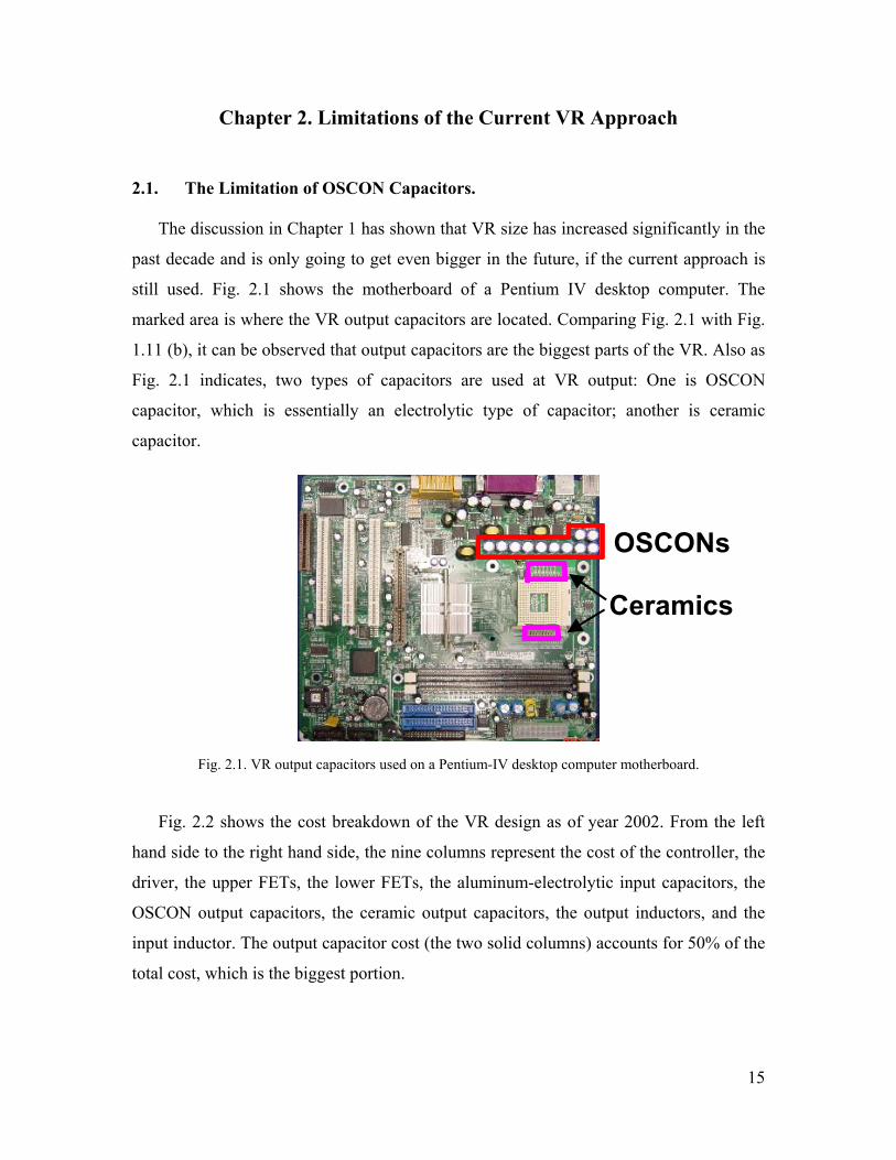
The discussion in Chapter 1 has shown that VR size has increased significantly in the
past decade and is only going to get even bigger in the future, if the current approach is
still used. Fig. 2.1 shows the motherboard of a Pentium IV desktop computer. The
marked area is where the VR output capacitors are located. Comparing Fig. 2.1 with Fig.
1.11 (b), it can be observed that output capacitors are the biggest parts of the VR. Also as
Fig. 2.1 indicates, two types of capacitors are used at VR output: One is OSCON
capacitor, which is essentially an electrolytic type of capacitor; another is ceramic
capacitor.
OSCONs
Ceramics
Fig. 2.1. VR output capacitors used on a Pentium-IV desktop computer motherboard.
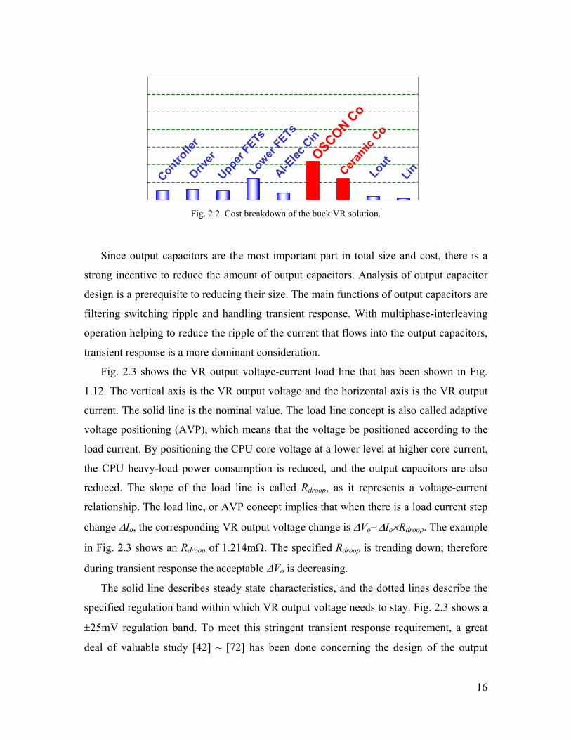
Fig. 2.2 shows the cost breakdown of the VR design as of year 2002. From the left
hand side to the right hand side, the nine columns represent the cost of the controller, the
driver, the upper FETs, the lower FETs, the aluminum-electrolytic input capacitors, the
OSCON output capacitors, the ceramic output capacitors, the output inductors, and the
input inductor. The output capacitor cost (the two solid columns) accounts for 50% of the
total cost, which is the biggest portion.
16
Contro
ller
Driver
Upper FETs
Lower FETs
Al-Elec
Cin
Ceramic
CoLoutLin
OSCON Co
Fig. 2.2. Cost breakdown of the buck VR solution.
Since output capacitors are the most important part in total size and cost, there is a
strong incentive to reduce the amount of output capacitors. Analysis of output capacitor
design is a prerequisite to reducing their size. The main functions of output capacitors are
filtering switching ripple and handling transient response. With multiphase-interleaving
operation helping to reduce the ripple of the current that flows into the output capacitors,
transient response is a more dominant consideration.
Fig. 2.3 shows the VR output voltage-current load line that has been shown in Fig.
1.12. The vertical axis is the VR output voltage and the horizontal axis is the VR output
current. The solid line is the nominal value. The load line concept is also called adaptive
voltage positioning (AVP), which means that the voltage be positioned according to the
load current. By positioning the CPU core voltage at a lower level at higher core current,
the CPU heavy-load power consumption is reduced, and the output capacitors are also
reduced. The slope of the load line is called Rdroop, as it represents a voltage-current
relationship. The load line, or AVP concept implies that when there is a load current step
change ∆Io, the corresponding VR output voltage change is ∆Vo=∆Io×Rdroop. The example
in Fig. 2.3 shows an Rdroop of 1.214mΩ. The specified Rdroop is trending down; therefore
during transient response the acceptable ∆Vo is decreasing.
The solid line describes steady state characteristics, and the dotted lines describe the
specified regulation band within which VR output voltage needs to stay. Fig. 2.3 shows a
±25mV regulation band. To meet this stringent transient response requirement, a great
deal of valuable study [42] ~ [72] has been done concerning the design of the output

17
capacitors. Reference [65] discusses that AVP essentially means that the output
impedance of the VR is not zero in frequency domain. Fig. 2.4 (a) shows the equivalent
circuit of the VR, represented as an ideal voltage source in series with output impedance
equal to Ro. The load is represented by a current source. Fig. 2.4 (b) shows the output
voltage and current waveforms of the VR. If Ro is equal to the specified Rdroop of the load
line, the output voltage vo will changes with the magnitude equal to ∆Io×Rdroop whenever
the load current io changes with magnitude of ∆Io. In the ideal case, vo does not have any
overshoot or undershoot, and is always within the regulation band. From this illustration,
it can be seen that it is very beneficial to design the VR output impedance to be constant
as Rdroop. It can be seen that frequency domain analysis gives clearer insight of the
function of output capacitors. That being said, none of the previous studies discuss the
mixture of different types of output capacitors in frequency domain.
1.11.121.141.161.181.2
1.221.241.261.281.3
0 10 20 30 40 50 60 70 80 90Output Current
Cor
e Vo
ltage
NominalM ax.M in.
Rdroop
Fig. 2.3. A load line example from Intel VR10 spec.
VR CPU
iO
+
-
VO
RO
Vmax
VR CPU
iO
+
-
VO
RO
Vmax
(a)
18
iO
Vmax
Vmin
∆IO
VO ∆VO
iO
Vmax
Vmin
∆IO
VO ∆VO
(b)
Fig. 2.4. The constant output impedance of the VR means perfect transient response: (a) the equivalent
circuit, and (b) the output voltage current waveforms.
The output capacitor is a part of the VR, so it contributes to VR output impedance.
Fig. 2.5 (a) shows the equivalent circuit of a capacitor. It consists of three parts: the pure
capacitor C, the equivalent series R (ESR) and the equivalent series L (ESL). An OSCON
capacitor is essentially an electrolytic capacitor. It features large capacitance and a
relatively low ESR value and a relatively low ESL value. A ceramic capacitor has even
lower ESR and ESL than an OSCON capacitor, but also has lower capacitance.
Fig. 2.5 (b) shows an asymptotic impedance curve of the capacitor according to the
model shown in Fig. 2.5 (a). There are two zeros in the curve. Roughly speaking the ESR
and the C form the first zero (fz1); and the ESR and the ESL form the second (fz2). The
mathematic expressions are
CESRf z ⋅⋅
≈π2
11 (2.1)
and
ESLESRf z ⋅
≈π22 (2.2)
Using the OSCON capacitor as an example: C=820µF, ESR=12mΩ, ESL=4nH; some
simple calculation gives that fz1=16KHz and fz2=477KHz. The capacitor impedance is
dominated by different parameters in different frequency ranges. Below fz1 the
capacitance C dominates; between fz1 and fz2 the ESR dominates and beyond fz2 the ESL
dominates. Fig. 2.5 (c) shows the frequency characteristic of an 820µF/4V OSCON
capacitor. Fig. 2.5 (d) shows the frequency characteristic of a ceramic capacitor. A

19
ceramic capacitor also has ESR and ESL, but the zeros fz1 and fz2 are not very distinct and
they are located in the MHz range, which is much higher than those of OSCON
capacitors.
ESR
ESL
C
f
Z
ESR
0 f z1 f z2
(a) (b)
100 1K 10K 100K 1M 10M0.01
0.1
1
10
Frequency(Hz)
Impe
danc
e(Ω
)
100 1K 10K 100K 1M 10M0.01
0.1
1
10
Frequency(Hz)
Impe
danc
e(Ω
)
(c)
100 1K 10K 100K 1M 10M0.001
0.01
0.1
1
Frequency(Hz)
Impe
danc
e(Ω
)
10
100
1000
100 1K 10K 100K 1M 10M0.001
0.01
0.1
1
Frequency(Hz)
Impe
danc
e(Ω
)
10
100
1000
(d)
Fig. 2.5. The frequency characteristic of an OSCON capacitor: (a) the capacitor model, (b)
the asymptotic curve of capacitor impedance, (c) the impedance curve of an OSCON
capacitor, and (d) the impedance curve of an OSCON capacitor.
20
The current desktop VRs use OSCON capacitors. Fig. 2.6 (a) shows a multiphase
buck VR with pure OSCON capacitors at the output. The VR output impedance is shown
in Fig. 2.6 (b). The dashed curve marked as Zc is the output capacitor characteristic. The
solid curve marked as Zo-open is the VR open-loop output impedance. Zo-open is the parallel
of output choke inductor impedance and output capacitor impedance. At low frequency
Zo-open follows the output choke inductor ESR, then the choke inductor L, then the L-C
resonance of the choke inductor and the output capacitor. After the resonance Zo-open
follows the output capacitor characteristic.
Given the shape of Zo-open, close-loop control is necessary to flatten it. Fig. 2.7 (a)
shows the close-loop buck VR. When the control loop is effective, there is an important
parameter the control bandwidth fc. What fc can do is illustrated in Fig. 2.7 (b). The
dashed line Zc is the output capacitor characteristic and the dashed line Zo-open is the VR
open-loop output impedance. The solid curve Zo-close is the VR close-loop output
impedance. Within the control bandwidth fc, correct design of the compensator can make
the output impedance constant. However, Zo-close beyond fc can only follow Zo-open, as the
close loop gain is less than 0dB and therefore is no longer effective.
The first zero fz1 of the OSCON capacitor is located at 20KHz. When there is fc ≥ fz1,
the scenario is like the solid curve shown in Fig. 2.8: Within fc, Zo-close is shaped by the
control loop to be constant, between fc and the second zero fz2 of the OSCON capacitor
(≈500KHz), Zo-close is the ESR of the OSCON capacitor, and therefore is also
approximately constant. Beyond fz2, Zo-close is dominated by the ESL effect of the OSCON
capacitor and goes up.
The Zo-close curve in Fig. 2.8 is based on that only one OSCON capacitor is used. One
OSCON capacitor has an ESR=12mΩ. This value is much larger than the required Rdroop.
The dashed line is one example of the desired Zo-close=Rdroop=1.214mΩ. It can be seen that
the solid line Zo-close is higher than Rdroop.

21
VinQ2Q1
Q4Q3
Q6Q5
Q8Q7
L
L
L
L
Zo-open(s)
(a)
f
Z
0
Zc
Zo-open
(b)
Fig. 2.6. VR open loop output impedance: (a) the open-loop buck VR using OSCON capacitors; and (b)
the open-loop output impedance of the VR.
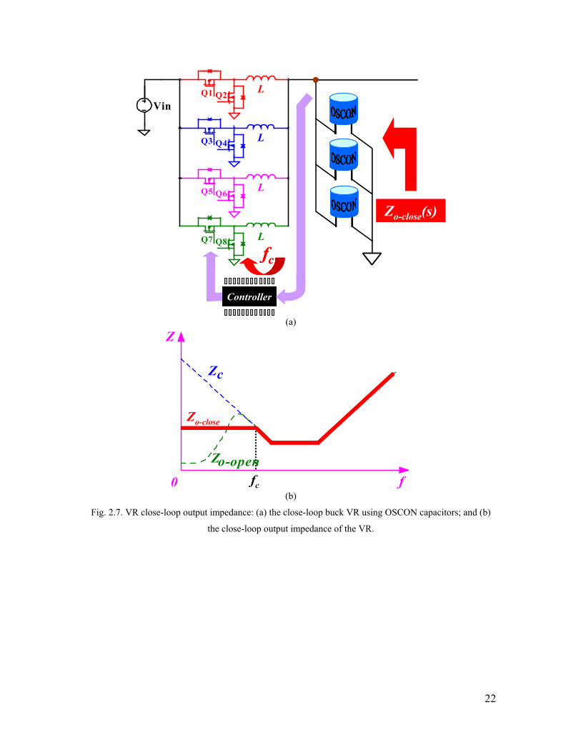
22
VinQ2Q1
Q4Q3
Q6Q5
Q8Q7
L
L
L
L
ControllerController
fcfc
Zo-close(s)
(a)
f
Z
0
Zc
Zo-open
Zo-close
fc (b)
Fig. 2.7. VR close-loop output impedance: (a) the close-loop buck VR using OSCON capacitors; and (b)
the close-loop output impedance of the VR.

23
f
Z
0
Zc
20K 500K
Zo-close
fc
Ωm12
droopR
Fig. 2.8. Today’s VR close-loop output impedance using one OSCON capacitor.
The way to bring Zo-close down to the value of Rdroop is to parallel multiple OSCON
capacitors. The dashed line marked as Zc in Fig. 2.9 (a) is the characteristic of the
paralleled OSCON capacitors. Although fz1 and fz2 don’t change after paralleling of the
capacitors, the equivalent ESR is reduced to OSCON
OSCONn
ESR , where ESROSCON is the
ESR of a single OSCON capacitor and nOSCON is the number of OSCON capacitors. By
paralleling OSCON capacitors, Zc curve in Fig. 2.9 (a) shifts down compared with that in
Fig. 2.8. The correct number of OSCON capacitors is given by
droop
OSCONOSCON R
ESRn ≈ (2.3)
The solid line in Fig. 2.9 (a) is Zo-close after paralleling OSCON capacitors. Up to
500KHz, Zo-close is kept at Rdroop. Given ESROSCON =12mΩ and Rdroop =1.214mΩ, the
needed nOSCON ≈11. This can be verified by counting the number of OSCON capacitors
on today’s Pentium IV desktop computer motherboard as shown in Fig. 2.9 (b).
24
f
Z
0
Zc
20K 500K
Zo-close
fc
droopR
ESR OSCONnOSCON=
(a)
1112 Ω
≈mRdroop
(b)
Fig. 2.9. Use multiple OSCON capacitors to achieve Rdroop: (a) the output impedance when multiple
OSCON capacitors are paralleled; and (b) a desktop motherboard practice.
The Zo-close shown in Fig. 2.9 (a) is theoretically kept at Rdroop up to 500 KHz, but
eventually goes up due to the ESL effect of OSCON capacitors. The bode-plot in Fig.
2.10 shows a switching-model simulation result of the Zo-close. Eleven OSCON capacitors
are used and the control bandwidth fc is 50KHz. It is seen that Zo-close is larger than Rdroop
in the excess of 120KHz range. The load current step change is from 70A to 0A @
400A/µs. The VR can be viewed as a voltage source in series with output impedance
consisting of a resistor of Rdroop in series with an inductor of ESLOSCON/nOSCON. Fig. 2.11
(a) shows the simulation result of Vo based on the simplified equivalent circuit shown in
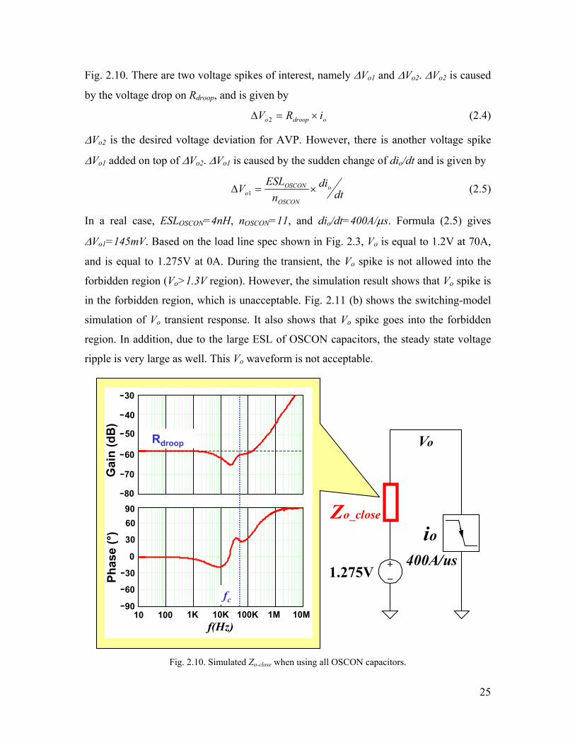
25
Fig. 2.10. There are two voltage spikes of interest, namely ∆Vo1 and ∆Vo2. ∆Vo2 is caused
by the voltage drop on Rdroop, and is given by
odroopo iRV ×=∆ 2 (2.4)
∆Vo2 is the desired voltage deviation for AVP. However, there is another voltage spike
∆Vo1 added on top of ∆Vo2. ∆Vo1 is caused by the sudden change of dio/dt and is given by
dtdi
nESL
V o
OSCON
OSCONo ×=∆ 1 (2.5)
In a real case, ESLOSCON=4nH, nOSCON=11, and dio/dt=400A/µs. Formula (2.5) gives
∆Vo1=145mV. Based on the load line spec shown in Fig. 2.3, Vo is equal to 1.2V at 70A,
and is equal to 1.275V at 0A. During the transient, the Vo spike is not allowed into the
forbidden region (Vo>1.3V region). However, the simulation result shows that Vo spike is
in the forbidden region, which is unacceptable. Fig. 2.11 (b) shows the switching-model
simulation of Vo transient response. It also shows that Vo spike goes into the forbidden
region. In addition, due to the large ESL of OSCON capacitors, the steady state voltage
ripple is very large as well. This Vo waveform is not acceptable.
1.275V
io
400A/us
Vo
Zo_close
Rdroop
Gai
n (d
B)
30
40
60
70
50
80
f(Hz)
fc
Phas
e (°
)
10 100 1K 10K 100K 1M 10M
9060
0
30
90
30
60
---
------
Fig. 2.10. Simulated Zo-close when using all OSCON capacitors.
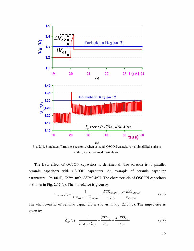
26
1.1
1.2
1.3
1.4
1.5
19 20 21 22 23 24t (us)
Vo
(V)
Forbidden Region !!!
∆Vo1
∆Vo2
(a)
1.10
1.15
1.20
1.25
1.30
1.35
1.40
10 20 30 40 50 60
V o(V
)
t(us)
Io step: 0~70A, 400A/us
Forbidden Region !!!
(b)
Fig. 2.11. Simulated Vo transient response when using all OSCON capacitors: (a) simplified analysis,
and (b) switching model simulation.
The ESL effect of OCSON capacitors is detrimental. The solution is to parallel
ceramic capacitors with OSCON capacitors. An example of ceramic capacitor
parameters: C=100µF, ESR=1mΩ, ESL=0.4nH. The characteristic of OSCON capacitors
is shown in Fig. 2.12 (a). The impedance is given by
OSCON
OSCON
OSCON
OSCON
OSCONOSCONOSCON n
ESLsn
ESRCns
sZ⋅
++⋅⋅
=1)( (2.6)
The characteristic of ceramic capacitors is shown in Fig. 2.12 (b). The impedance is
given by
cer
cer
cer
cer
cercercer n
ESLsn
ESRCns
sZ⋅
++⋅⋅
=1)( (2.7)
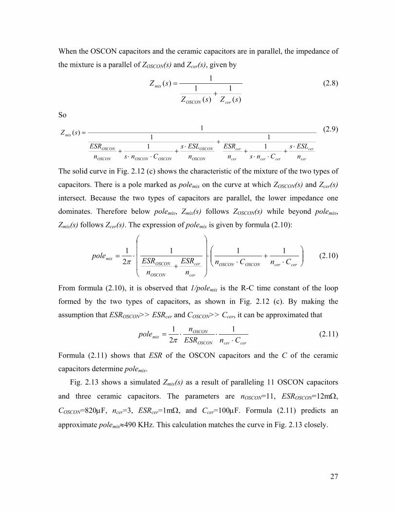
27
When the OSCON capacitors and the ceramic capacitors are in parallel, the impedance of
the mixture is a parallel of ZOSCON(s) and Zcer(s), given by
)(1
)(1
1)(
sZsZ
sZ
cerOSCON
mix
+= (2.8)
So
cer
cer
cercercer
cer
OSCON
OSCON
OSCONOSCONOSCON
OSCON
mix
nESLs
CnsnESR
nESLs
CnsnESR
sZ
⋅+
⋅⋅+
+⋅
+⋅⋅
+
=
11
11
1)( (2.9)
The solid curve in Fig. 2.12 (c) shows the characteristic of the mixture of the two types of
capacitors. There is a pole marked as polemix on the curve at which ZOSCON(s) and Zcer(s)
intersect. Because the two types of capacitors are parallel, the lower impedance one
dominates. Therefore below polemix, Zmix(s) follows ZOSCON(s) while beyond polemix,
Zmix(s) follows Zcer(s). The expression of polemix is given by formula (2.10):
⋅
+⋅
⋅
+⋅=
cercerOSCONOSCON
cer
cer
OSCON
OSCONmix CnCn
nESR
nESR
pole 11121π
(2.10)
From formula (2.10), it is observed that 1/polemix is the R-C time constant of the loop
formed by the two types of capacitors, as shown in Fig. 2.12 (c). By making the
assumption that ESROSCON>> ESRcer and COSCON>> Ccer, it can be approximated that
cercerOSCON
OSCONmix CnESR
npole
⋅⋅⋅=
121π
(2.11)
Formula (2.11) shows that ESR of the OSCON capacitors and the C of the ceramic
capacitors determine polemix.
Fig. 2.13 shows a simulated Zmix(s) as a result of paralleling 11 OSCON capacitors
and three ceramic capacitors. The parameters are nOSCON=11, ESROSCON=12mΩ,
COSCON=820µF, ncer=3, ESRcer=1mΩ, and Ccer=100µF. Formula (2.11) predicts an
approximate polemix≈490 KHz. This calculation matches the curve in Fig. 2.13 closely.
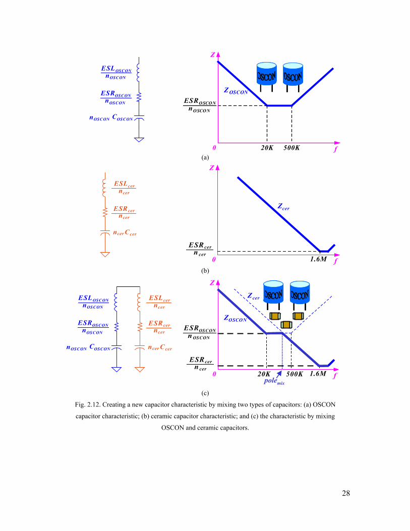
28
ESROSCONnOSCON
ESLOSCONnOSCON
nOSCON COSCON
f
Z
0 20K 500K
Z OSCON
ESROSCONnOSCON
(a)
ncer
ncer
ESRcer
Ccer
ncer
ESLcer
f
Z
0 1.6M
ESRn
cercer
Zcer
(b)
ESROSCONnOSCON
ESLOSCONnOSCON
nOSCON COSCON
ncer
ncer
ESRcer
Ccer
ncer
ESLcer
f
Z
0 20K 500K
Zcer
1.6M
ZOSCON
ESROSCONn OSCON
ESRn
cercer
polemix (c)
Fig. 2.12. Creating a new capacitor characteristic by mixing two types of capacitors: (a) OSCON
capacitor characteristic; (b) ceramic capacitor characteristic; and (c) the characteristic by mixing
OSCON and ceramic capacitors.

29
f(Hz)10 100 1K 10K 100K 1M 10M
Gai
n (d
B)
0
20
60
40
80
Phas
e (°
)
9060
0
30
90
30
60
---
-
-
-
-
Fig. 2.13. A simulated Zmix(s) of the mixture of OSCON capacitors and ceramic capacitors.
Mixing ceramic capacitors with OSCON capacitors creates a new characteristic,
which helps to reduce or even get rid of the ESL effect of OSCON capacitors. With more
ceramic capacitors used, Zcer(s) is more toward the left-hand side and polemix is located at
a lower frequency. There are three possible scenarios associated with different amounts
of ceramic capacitors used.
Fig. 2.14 (a) shows the case when too few ceramic capacitors are used. The solid line
is Zmix(s). In this case, because Zcer(s) intersects ZOSCON(s) after the fz2 of OSCON
capacitors (500KHz), Zmix(s) has a bump after 500KHz, which includes the ESL
information of the OSCON capacitors.
Fig. 2.14 (b) shows that Zcer(s) intersects ZOSCON(s) right at the fz2 of OSCON
capacitors (500KHz) when a certain amount of ceramic capacitors are used. Then Zmix(s)
does not have a bump as in Fig. 3.17 (a).

30
Fig. 2.14 (c) shows that when more ceramic capacitors are used, Zcer(s) intersects
ZOSCON(s) before the fz2 of OSCON capacitors (500KHz), and Zmix(s) does not have a
bump either.
It is very easy for today’s practice to achieve a control bandwidth fc higher than fz1 of
OSCON capacitors (20KHz), but very difficult to achieve an fc higher than the fz2 of
OSCON capacitors (500KHz). Fig. 2.15 (a)~(c) show the VR close-loop output
impedance Zo-close(s) corresponding to the capacitor characteristics shown in Fig. 2.14.
The fact is that Zo-close(s) is controlled to be the desired Rdroop within fc and follows Zmix(s)
beyond fc. Fig. 2.15 (a) shows the Zo-close(s) corresponding to the Zmix(s) of Fig. 2.14 (a); it
is observed that Zo-close(s) has a bump with a value higher than Rdroop. Fig. 2.15 (b) shows
the Zo-close(s) corresponding to the Zmix(s) of Fig. 2.14 (b); it is observed that Zo-close(s) has
no bump. Fig. 2.15 (c) shows the Zo-close(s) corresponding to the Zmix(s) of Fig. 2.14 (c); it
is observed that Zo-close(s) has no bump either. It can also be seen that Fig. 2.15 (b) already
eliminates the ESL effect of OSCONS capacitors and uses fewer ceramic capacitors than
Fig. 2.15 (c). So the design in Fig. 2.15 (c) uses more than adequate ceramic capacitors
thus is undesirable.
Fig. 2.15 (b) is the case that uses such amount of ceramic capacitors that it satisfies
polemix=fz2_OSCON, where fz2_OSCON is the fz2 of OSCON capacitors. Therefore equalize
formulas (2.2) and (2.11)
OSCON
OSCON
cercerOSCON
OSCON
ESLESR
CnESRn
⋅=
⋅⋅⋅
ππ 21
21 (2.12)
the solution is
OSCON
OSCON
OSCON
OSCONcercer ESR
ESLESR
nCn ⋅=⋅ (2.13)
Because it has already been determined that the number of OSCON capacitors is dictated
by
droop
OSCONOSCON R
ESRn = (2.14)
formula (2.13) can be further expressed as
OSCONdroop
OSCONcercer ESRR
ESLCn
⋅=⋅ (2.15)
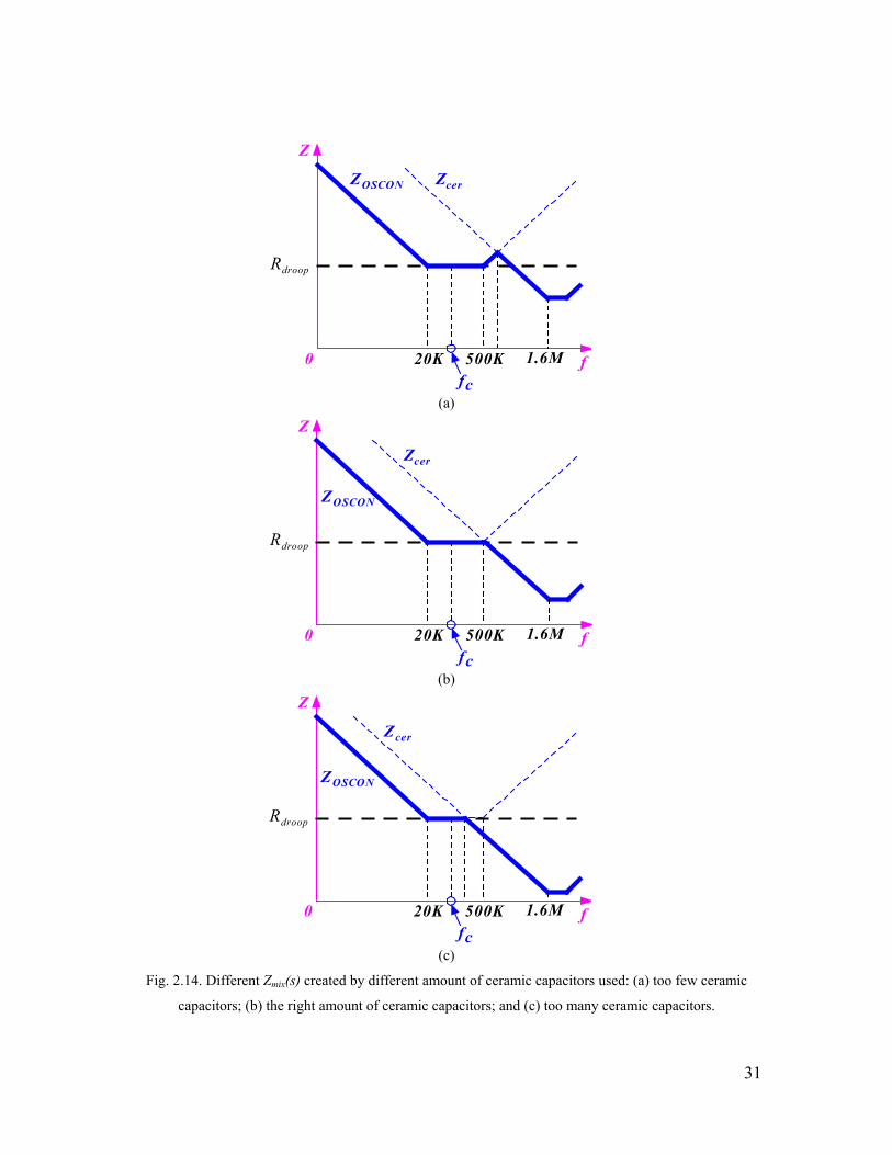
31
f
Z
0
ZOSCON
20K 500Kfc
droopR
Zcer
1.6M
(a)
f
Z
0
ZOSCON
20K 500Kfc
droopR
Zcer
1.6M
(b)
f
Z
0
ZOSCON
20K 500Kfc
droopR
Zcer
1.6M
(c)
Fig. 2.14. Different Zmix(s) created by different amount of ceramic capacitors used: (a) too few ceramic
capacitors; (b) the right amount of ceramic capacitors; and (c) too many ceramic capacitors.

32
f
Z
0
Zmix
20K 500K
Zo-close
fc
droopR
1.6M
(a)
f
Z
0
Zm ix
20K 500K
Zo-close
fc
droopR
1.6M
(b)
f
Z
0
Zm ix
20K 500K
Zo-close
fc
droopR
1.6M
(c)
Fig. 2.15. Different Zo-close(s) created by different amount of ceramic capacitors used: (a) too few ceramic
capacitors; (b) the right amount of ceramic capacitors; and (c) too many ceramic capacitors.
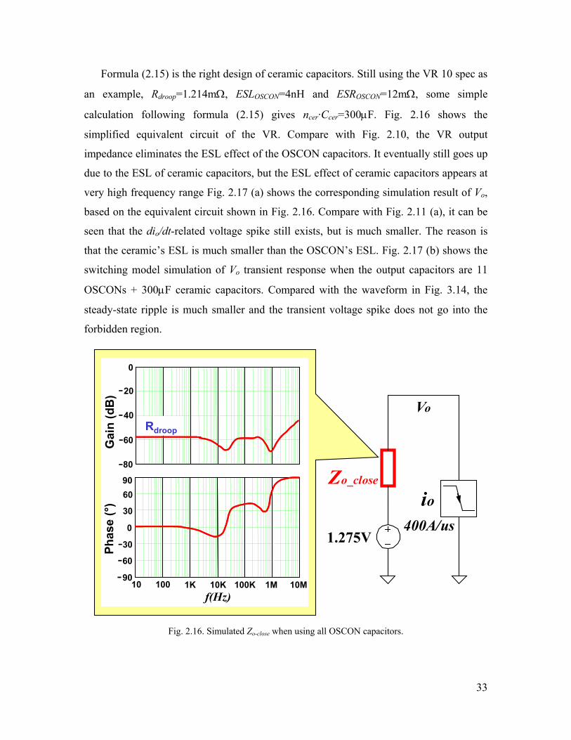
33
Formula (2.15) is the right design of ceramic capacitors. Still using the VR 10 spec as
an example, Rdroop=1.214mΩ, ESLOSCON=4nH and ESROSCON=12mΩ, some simple
calculation following formula (2.15) gives ncer·Ccer=300µF. Fig. 2.16 shows the
simplified equivalent circuit of the VR. Compare with Fig. 2.10, the VR output
impedance eliminates the ESL effect of the OSCON capacitors. It eventually still goes up
due to the ESL of ceramic capacitors, but the ESL effect of ceramic capacitors appears at
very high frequency range Fig. 2.17 (a) shows the corresponding simulation result of Vo,
based on the equivalent circuit shown in Fig. 2.16. Compare with Fig. 2.11 (a), it can be
seen that the dio/dt-related voltage spike still exists, but is much smaller. The reason is
that the ceramic’s ESL is much smaller than the OSCON’s ESL. Fig. 2.17 (b) shows the
switching model simulation of Vo transient response when the output capacitors are 11
OSCONs + 300µF ceramic capacitors. Compared with the waveform in Fig. 3.14, the
steady-state ripple is much smaller and the transient voltage spike does not go into the
forbidden region.
f(Hz)10 100 1K 10K 100K 1M 10M
Gai
n (d
B)
0
20
60
40
80
Phas
e (°
)
9060
0
30
90
30
60
---
-
-
-
-
Rdroop
1.275V
io
400A/us
Vo
Zo_close
Fig. 2.16. Simulated Zo-close when using all OSCON capacitors.

34
1.1
1.2
1.3
1.4
1.5
19 20 21 22 23 24t (us)
Vo
(V)
Forbidden Region !!!
(a)
1.10
1.15
1.20
1.25
1.30
1.35
1.40
10 20 30 40 50 60
V o(V
)
t(us)
Io step: 0~70A, 400A/us
Forbidden Region !!!
(b)
Fig. 2.17. Simulated Vo transient response when using 11 OSCONs plus 300µF ceramic capacitors: (a)
simplified analysis, and (b) switching model simulation.
It is now clear that using OSCON capacitors plus ceramic capacitors is an option for
VR output capacitors. The number of OSCON capacitors is given by formula (2.14) and
the number of ceramic capacitors is given by formula (2.15). This approach has several
limitations:
(1). OSCON capacitors have large ESR. The ESR determines the number of
OSCON capacitors needed, and the capacitance is actually more than needed.
(2). OSCON capacitors have large ESL, which requires substantial amount of
ceramic capacitors to suppress.
(3). OSCON capacitors are large. This fact makes VR take up a large space on
desktop computer motherboard.

35
(4). The control bandwidth needs to be higher than 20KHz, but further pushing up
does not reduce the number of capacitors.
If the current approach still applies, to meet the voltage regulation band requirement,
a lot more capacitors will be needed at the output to handle the transient response. Fig.
2.18 shows an estimation of capacitors needed for future VRs. For example, for a future
VR with 0.8V/150A output, 30 OSCON capacitors and quite a lot of ceramic capacitors
are needed. The VR takes almost 30% of the space on the motherboard, as opposed to
12% in Fig. 1.10 (b). This is unacceptable. Fig. 2.19 shows the cost comparison of the
current solution and the future solution. The total cost increases by more than 100% of
the cost of current solution. In addition, the output capacitor cost accounts for 65.3% of
the total cost.
OSCON capacitors don’t seem to be suitable as future VR output capacitors due to
their inherent limitations.
Fig. 2.18. Capacitors needed for future VRs.
Contro
ller
Driver
Upper
FETsLow
er FE
TsAl-E
lec C
in
Ceramic
CoLou
tLin
OSCON ConowFuturenowFuture
Fig. 2.19. Cost estimation for future VRs.
36
2.2. The Limitation of Low Switching Frequency.
The previous discussion has analyzed the desktop computer VR solution, which uses
OSCON capacitors. OSCON capacitors are electrolytic type of capacitors, so they have
low reliability. This is a big concern in some reliability-sensitive applications, such as
servers. In servers, VR output capacitors are all ceramic capacitors as they have higher
reliability. An additional benefit is that ceramic capacitors have low ESR and ESL, which
establishes them as a good solution to overcome OSCON capacitor’s inherent limitations.
The design of all-ceramic capacitors is explained as follows. Fig. 2.20 (a) shows the
ceramic capacitor impedance curve Zcer. It mainly is the capacitance; the ESR is very low
and the ESL effect shows up at very high frequency range. Rdroop is the desired VR output
impedance. The solid line in Fig. 2.20 (b) shows the open-loop VR impedance Zo-open. At
low frequency Zo-open follows the output choke inductor ESR, then the L-C resonance of
the choke inductor and the output ceramic capacitor. After the resonance Zo-open follows
the output ceramic capacitor characteristic. Fig. 2.20 (c) shows the close-loop VR output
impedance Zo-close. The control loop sets its bandwidth fc at the higher one of the two
frequencies where Rdroop intersects Zo-open. By correct design of the control loop
compensator, Zo-close is controlled to be Rdroop within fc, and follows Zcer thereafter. It can
be seen that Zo-close eventually goes up due to the ESL effect of the ceramic capacitor. But
as previously discussed, the ESL effect of the ceramic capacitor is not an issue at VR
output. So the Zo-close shape should be able to give a good transient response. The amount
of ceramic capacitance is given by
cdroopcercer fR
Cn⋅⋅
=⋅π2
1 (2.16)
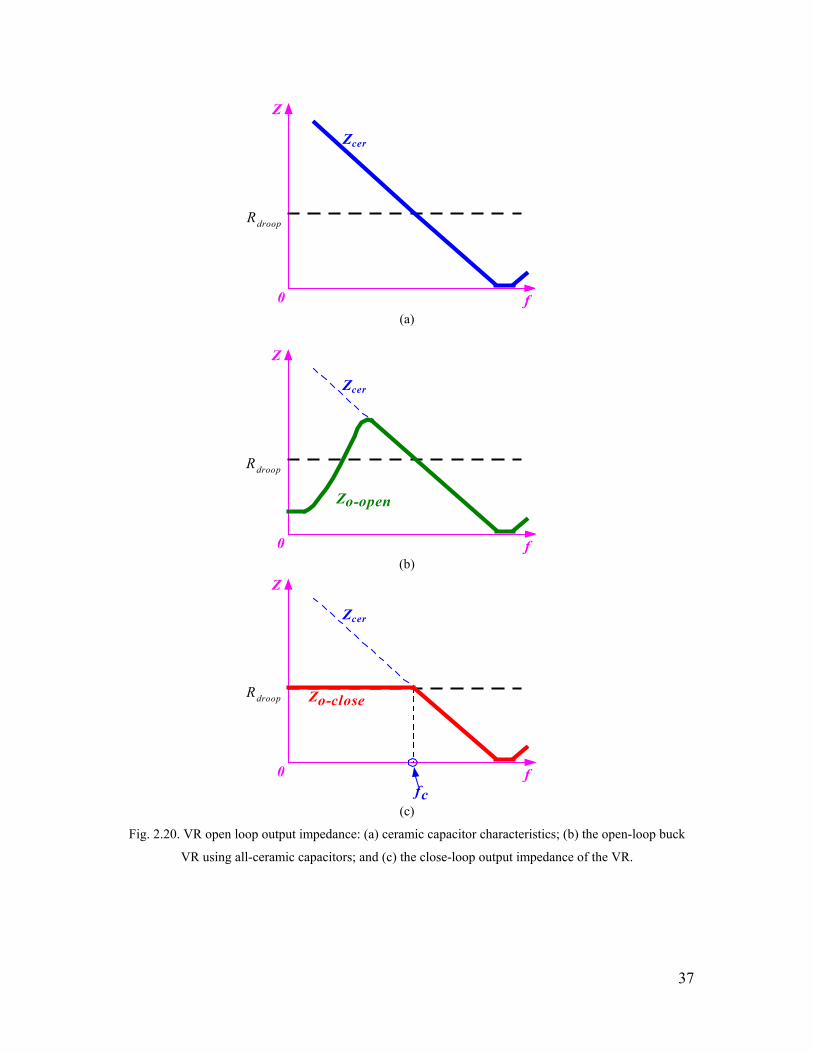
37
f
Z
0
droopR
Zcer
(a)
f
Z
0
droopR
Zcer
Zo-open
(b)
f
Z
0
Zo-close
fc
droopR
Zcer
(c)
Fig. 2.20. VR open loop output impedance: (a) ceramic capacitor characteristics; (b) the open-loop buck
VR using all-ceramic capacitors; and (c) the close-loop output impedance of the VR.

38
The dashed curve in Fig. 2.21 shows the ceramic capacitor impedance curve Zcer and
the solid curve in Fig. 2.21 shows the VR close-loop output impedance Zo-close obtained
through a switching-model simulation. It can be seen that Zo-close is kept at Rdroop until
approximately 50KHz and follows Zo-close thereafter. It is also noted that Zo-close eventually
goes up due to the ESL of the ceramic capacitor, but the ESL effect of ceramic capacitors
appears at very high frequency range. Fig. 2.22 (a) shows the simplified equivalent circuit
of the VR and Fig. 2.22 (b) shows the corresponding simulation result of Vo. Comparing
with Fig. 2.17 (a), it can be seen that the dio/dt-related voltage spike is much smaller. The
reason is that the ceramic’s ESL is much smaller than the OSCON’s ESL. Fig. 2.23
shows the switching model simulation of Vo transient response when the output
capacitors are 800µF ceramic capacitors. The transient voltage spike does not go into the
forbidden region.
f(Hz)10 100 1K 10K 100K 1M 10M
Gai
n (d
B)
30
70
40
80
Phas
e (°
)
9060
0
30
90
30
60
---
--
--
50
60--
Zcer
Zo_close
Zcer
Zo_close
Fig. 2.21. Ceramic capacitor characteristics and the simulated Zo-close.

39
1.275V
io
400A/us
Vo
Zo_close
f(Hz)10 100 1K 10K 100K 1M 10M
Phas
e (°
)
9060
0
30
90
30
60
---
Gai
n (d
B)
30
70
40
80--
--
50
60-- Rdroop
(a)
1.1
1.2
1.3
1.4
1.5
19 20 21 22 23 24t (us)
Vo
(V)
Forbidden Region !!!
(b)
Fig. 2.22. Simplified VR equivalent circuit and the transient response: (a) VR equivalent circuit; and (b)
the transient response obtained through the equivalent circuit.

40
1.10
1.15
1.20
1.25
1.30
1.35
1.40
10 20 30 40 50 60
V o(V
)
t(us)
Io step: 0~70A, 400A/us
Forbidden Region !!!
Fig. 2.23. The switching model simulation result of Vo transient response.
The previous discussion has shown that there are two options for VR output
capacitors:
(1). Use OSCON capacitors plus some ceramic capacitors. Fig. 2.24 (a) explains
this option. The number of OSCON capacitors is given by formula (2.3) and
the ceramic capacitance is given by formula (2.15). The control bandwidth fc
needs to be higher than 20KHz, but further raising won’t help to reduce the
number of capacitors.
(2) Use all-ceramic capacitors. Fig. 2.24 (b) shows the all-ceramic solution. The
amount of ceramic capacitors is given by formula (2.16). The higher the
control bandwidth, the smaller amount of ceramic capacitors needed.
Fig. 2.25 shows the experimental test results to verify the theoretical prediction. The
design spec is the VR10 load line shown in Fig. 2.3. The switching frequency of the
multiphase buck VR is 1MHz. Fig. 2.25 (c) shows the load current, which steps down
from 60A to 0A with 60A/µs slew rate. Figs. 2.25 (a) and (b) are the VR output voltage
waveforms, and they correspond to the cases shown in Fig. 2.24 (a) and (b). The dashed
lines above which the graphs say “forbidden region” are where Vo=1.3V. Vo is 1.275 V at
a load of 0A, and is 1.19V at a load of 60A. Case Fig. 2.24 (a) uses 11 OSCON
capacitors plus 300µF ceramic capacitors, and has a good Vo waveform; Fig. 2.24 (b)
uses 800µF ceramic capacitors, and also has a good Vo waveform.
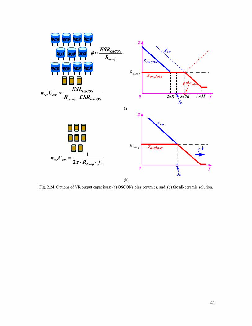
41
droop
OSCON
RESR
≈#
OSCONdroop
OSCONcercer ESRR
ESLCn⋅
≈
f
Z
0
Z OSCON
20K 500K
Zo-close
fc
droopR
Zcer
1.6M
polemix
(a)
cdroopcercer fR
Cn⋅⋅
=π2
1
f
Z
0
Zo-close
fc
droopR
Z cer
C
(b)
Fig. 2.24. Options of VR output capacitors: (a) OSCONs plus ceramics, and (b) the all-ceramic solution.

42
Forbidden Region
Vo
(a)
Forbidden Region
Vo
(b)
∆Io =60 A
(c)
Fig. 2.25. Experimental test results of the transient response: (a) OSCONs plus ceramics, (b) the all-
ceramic solution, and (c) the load current step change.
The two options for VR output capacitors are compared as regards footprint and size.
Assume the footprint area of an OSCON capacitor is AOSCON and the footprint area of a
ceramic capacitor is Acer. The total footprint area of the OSCON solution is
cerOSCONcerdroop
OSCONOSCON
droop
OSCONOSCON A
ESRCRESL
AR
ESRS ⋅
⋅⋅+⋅= (2.17)
and the total footprint area of the all-ceramic solution is
cercercdroop
cer ACfR
S ⋅⋅⋅⋅
=π2
1 (2.18)
Since the higher control bandwidth, the fewer ceramic capacitors needed for an all-
ceramic solution, there exists a bandwidth fc_A that makes Scer<SOSCON when fc>fc_A,
which means when fc>fc_A the all-ceramic solution takes smaller footprint area. This fc is
given by
⋅
+⋅⋅⋅=
cerOSCON
OSCONOSCON
cer
OSCONcer
Ac
CESRESL
ESRA
AC
fπ2
1_ (2.19)

43
For today’s situation, ESROSCON=12mΩ, ESLOSCON=4nH, AOSCON=0.163in2, Ccer=100µF,
and Acer=0.0216in2. A calculation based on formula (2.19) gives fc_A=17KHz. This
control bandwidth is very easy to achieve. If the control bandwidth is 1/6 of the switching
frequency, 17KHz bandwidth means about 100KHz switching frequency. So if the VR
can operate at above 100KHz, it will be able to use the all-ceramic solution as a smaller-
size solution.
Assume the cost of an OSCON capacitor is $OSCON and the cost of a ceramic capacitor
is $cer. The total cost of the OSCON solution is
cerOSCONcerdroop
OSCONOSCON
droop
OSCONOSCON ESRCR
ESLR
ESRCost $$ ⋅
⋅⋅+⋅= (2.20)
and the total cost of the all-ceramic solution is
cercercdroop
cer CfRCost $
21
⋅⋅⋅⋅
=π
(2.21)
Since the higher control bandwidth, the fewer ceramic capacitors needed for an all-
ceramic solution, there exists a bandwidth f$_A that makes Costcer<CostOSCON when
fc>f$_A. This means when fc>f$_A the all-ceramic solution is cheaper. It can be easily
derived that
+⋅⋅
=
OSCON
OSCONOSCON
cer
cer
OSCON
A
ESRESL
ESR
C
f
$$
2
1_$
π
(2.22)
As of year 2002, calculation based on formula (2.22) gives f$_A=170KHz. If the control
bandwidth is 1/6 of the switching frequency, 170KHz bandwidth means about 1MHz
switching frequency. So if the VR can operate at 1MHz, it will be able to use the all-
ceramic solution as a more cost-effective and smaller-size solution.
Fig. 2.26 (a) shows the cost comparison of the VRs operating at 300KHz. The
meshed columns are for the OSCON solution, and the solid columns are for the all-
ceramic solution. Because of the low switching frequency, the all-ceramic solution
requires quite a lot ceramic output capacitors The total cost of the all-ceramic solution
almost doubles that of the OSCON solution. Fig. 2.26 (b) shows the cost comparison of
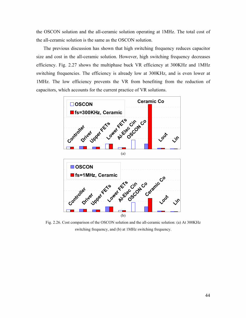
44
the OSCON solution and the all-ceramic solution operating at 1MHz. The total cost of
the all-ceramic solution is the same as the OSCON solution.
The previous discussion has shown that high switching frequency reduces capacitor
size and cost in the all-ceramic solution. However, high switching frequency decreases
efficiency. Fig. 2.27 shows the multiphase buck VR efficiency at 300KHz and 1MHz
switching frequencies. The efficiency is already low at 300KHz, and is even lower at
1MHz. The low efficiency prevents the VR from benefiting from the reduction of
capacitors, which accounts for the current practice of VR solutions.
OSCONfs=300KHz, Ceramic
Controlle
rDriv
erUppe
r FETs
Lower
FETs
Ceramic Co
LoutLinOSCON C
o
Al-Elec
Cin
(a)
OSCONfs=1MHz, Ceramic
Controlle
rDriv
erUpper
FETsLower
FETs
Ceramic
CoLou
tLinOSCON C
o
Al-Elec
Cin
(b)
Fig. 2.26. Cost comparison of the OSCON solution and the all-ceramic solution: (a) At 300KHz
switching frequency, and (b) at 1MHz switching frequency.
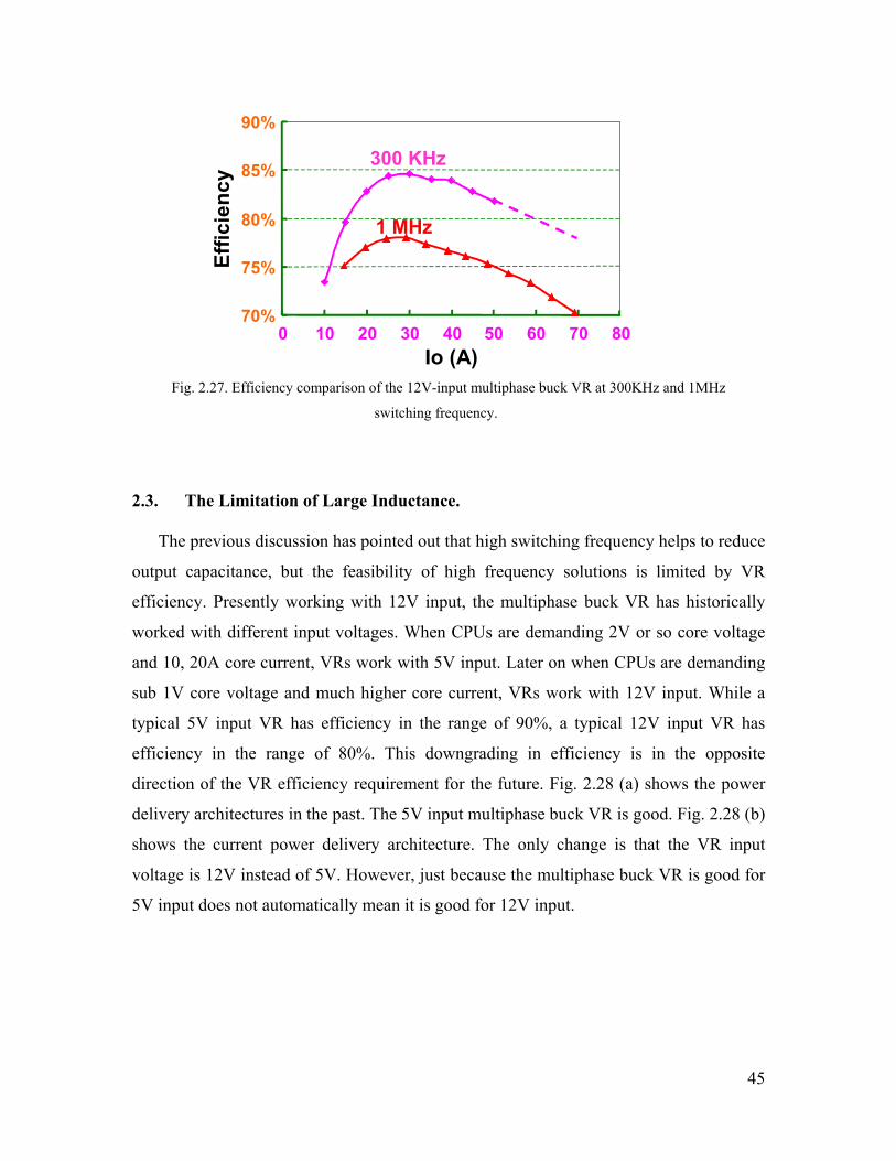
45
70%
75%
80%
85%
90%
0 10 20 30 40 50 60 70 80Io (A)
Effic
ienc
y
300 KHz
1 MHz
Fig. 2.27. Efficiency comparison of the 12V-input multiphase buck VR at 300KHz and 1MHz
switching frequency.
2.3. The Limitation of Large Inductance.
The previous discussion has pointed out that high switching frequency helps to reduce
output capacitance, but the feasibility of high frequency solutions is limited by VR
efficiency. Presently working with 12V input, the multiphase buck VR has historically
worked with different input voltages. When CPUs are demanding 2V or so core voltage
and 10, 20A core current, VRs work with 5V input. Later on when CPUs are demanding
sub 1V core voltage and much higher core current, VRs work with 12V input. While a
typical 5V input VR has efficiency in the range of 90%, a typical 12V input VR has
efficiency in the range of 80%. This downgrading in efficiency is in the opposite
direction of the VR efficiency requirement for the future. Fig. 2.28 (a) shows the power
delivery architectures in the past. The 5V input multiphase buck VR is good. Fig. 2.28 (b)
shows the current power delivery architecture. The only change is that the VR input
voltage is 12V instead of 5V. However, just because the multiphase buck VR is good for
5V input does not automatically mean it is good for 12V input.

46
Silver BoxAC
CPUCPU
CoQ2Q1
Q4Q3
L
L
itop vphase
Li
5VSilver Box
ACCPUCPU
CoQ2Q1
Q4Q3
L
L
itop vphase
Li
5V
(a)
Silver BoxAC
CPUCPU
CoQ2Q1
Q4Q3
L
L
itop vphase
Li
12VSilver Box
ACCPUCPU
CoQ2Q1
Q4Q3
L
L
itop vphase
Li
12V
(b)
Fig. 2.28. Power delivery architectures for desktop computers: (a) With 5V-input VRs, and (b)
with 12V-input VRs.
The duty cycle of a buck VR is given by
in
o
VV
D = (2.23)
where Vo is the output voltage and Vin is the input voltage. For example: for Vo=1.5V, the
duty cycle is 1.5/12=0.125 for a 12V-input buck VR, as opposed to 0.3 for a 5V-input
buck VR. It can be seen that after the VR input voltage switches from 5V to 12V, the
buck VR needs to work with a much smaller duty cycle due to the large step-down ratio.
This extreme duty cycle makes it difficult to design an efficient buck converter [16].

47
In order to facilitate the following discussion, some nomenclatures are defined as
shown in Fig. 2.28: iL is the inductor current, itop is the top switch current and vphase is the
so-called “phase voltage”.
Fig. 2.29 (a) ~ (d) show some key waveforms in a buck VR when the input voltage is
5V and 12V. The output voltage is 1.5V and the current is 12.5A per phase. Because
output capacitor Co cannot sustain DC current, the average value of iL is the load current
regardless the input voltage. However, the ripples of iL are different. Based on the
inductor current discharging period, the peak-to-peak iL ripple is given by
( )s
oL fL
DVi
⋅−⋅
=∆1
(2.24)
where L is the inductance, fs is the switching frequency, and D is the duty cycle. When
Vin moves from 5V to 12V, D becomes smaller; therefore ∆itop becomes larger. Fig. 2.29
(a) shows the inductor current iL. It is seen that with 12V input, iL has larger ripple. Given
the fact that the average value is the same, it can be understood that the peak value of iL is
higher with 12V input. Fig. 2.29 (b) shows the top switch current itop. Since itop is iL when
the top switch Q1 is conducting, it can be seen that the peak itop_pk is higher with 12V
input.
The turn-off loss of MOSFET Q1 is given by
sstressoffg
qsgdpktopoffturn fv
iQQ
iP ⋅⋅+
⋅=− _1
2_ (2.25)
where Qgd and Qgs2 are two gate charge parameters of Q1; voff_stress is the turn-off voltage
stress of Q1; ig1 is the gate current of Q1; and fs is the switching frequency. Since voff_stress
is theoretically the input voltage, it is higher with 12V input than with 5V input. After the
input voltage changes from 5V to 12V, itop_pk and voff_stress both increase, which
significantly increases the turn-off loss of the buck converter.
Fig. 2.29 (c) shows vphase waveform. vphase is Vin when Q1 is on, and is approximately
zero when Q1 is off. Because the output inductor cannot sustain DC voltage, the average
value of vphase is the output voltage Vo. The body-diode reverse recovery loss is given by
sonphaserrrr fVQP ⋅⋅= _ (2.26)
where Qrr is the reverse-recovery charge and vphase_on is the vphase value when Q1 is on.
Since vphase_on is theoretically the input voltage, it is higher with 12V input than with 5V
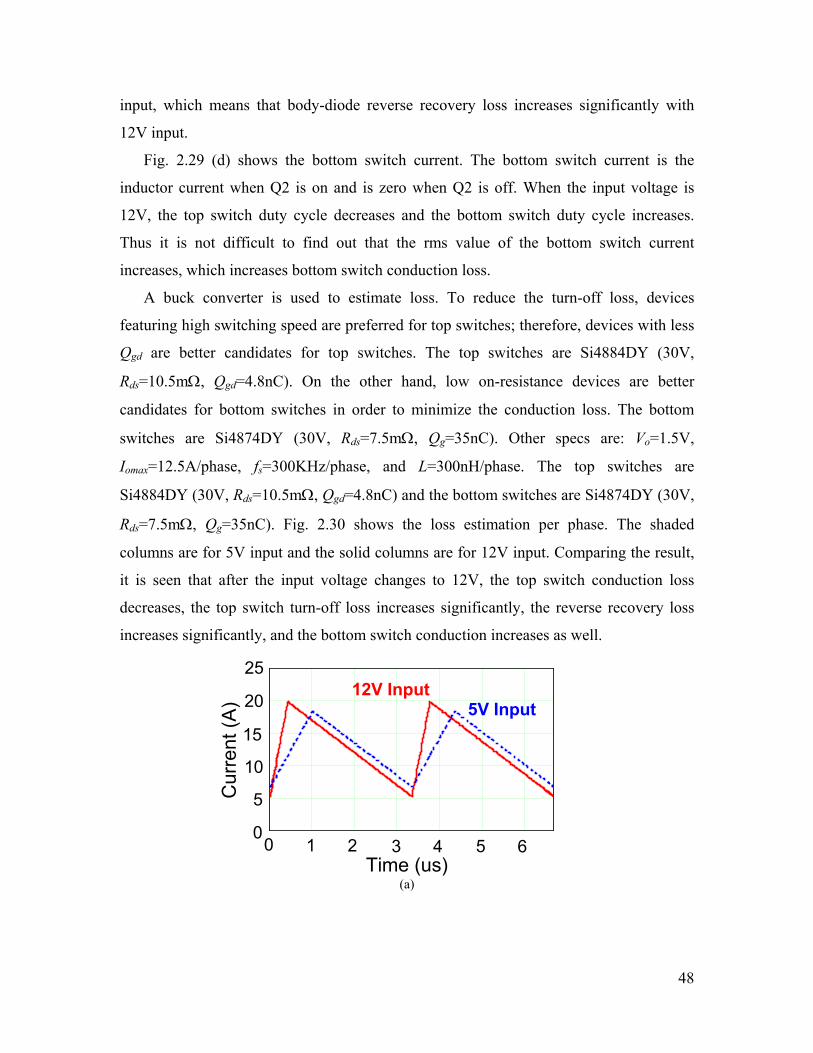
48
input, which means that body-diode reverse recovery loss increases significantly with
12V input.
Fig. 2.29 (d) shows the bottom switch current. The bottom switch current is the
inductor current when Q2 is on and is zero when Q2 is off. When the input voltage is
12V, the top switch duty cycle decreases and the bottom switch duty cycle increases.
Thus it is not difficult to find out that the rms value of the bottom switch current
increases, which increases bottom switch conduction loss.
A buck converter is used to estimate loss. To reduce the turn-off loss, devices
featuring high switching speed are preferred for top switches; therefore, devices with less
Qgd are better candidates for top switches. The top switches are Si4884DY (30V,
Rds=10.5mΩ, Qgd=4.8nC). On the other hand, low on-resistance devices are better
candidates for bottom switches in order to minimize the conduction loss. The bottom
switches are Si4874DY (30V, Rds=7.5mΩ, Qg=35nC). Other specs are: Vo=1.5V,
Iomax=12.5A/phase, fs=300KHz/phase, and L=300nH/phase. The top switches are
Si4884DY (30V, Rds=10.5mΩ, Qgd=4.8nC) and the bottom switches are Si4874DY (30V,
Rds=7.5mΩ, Qg=35nC). Fig. 2.30 shows the loss estimation per phase. The shaded
columns are for 5V input and the solid columns are for 12V input. Comparing the result,
it is seen that after the input voltage changes to 12V, the top switch conduction loss
decreases, the top switch turn-off loss increases significantly, the reverse recovery loss
increases significantly, and the bottom switch conduction increases as well.
25
20
15
10
5
01 20 3 4 5 6
Time (us)
Cur
rent
(A) 5V Input12V Input
(a)

49
25
20
15
10
5
01 20 3 4 5 6
Time (us)
Cur
rent
(A) 5V Input
12V Input
(b)
15
12
9
6
3
01 20 3 4 5 6
Time (us)
Vol
tage
(V)
5V Input
12V Input
(c)
25
20
15
10
5
01 20 3 4 5 6
Time (us)
Cur
rent
(A) 5V Input
12V Input
(d)
Fig. 2.29. Key waveforms in a buck VR when input voltage is 5 V and 12 V: (a) the inductor current, (b)
the top switch current, (c) the phase voltage, and (d) the bottom switch current.

50
0
0.4
0.8
1.2
1.6
TopConduction
TopTurn-off
ReverseRecovery
BottomConduction
Loss
(W)
5V Input
12V Input
Fig. 2.30. VR loss breakdown with 5V and 12V input voltage.
A VR input voltage change from 5V to 12V increases loss significantly, thus
dragging down VR efficiency. A four-phase interleaved buck VR prototype is built for
evaluation purposes. Fig. 2.31 shows a photograph of the prototype. Fig. 2.32 shows the
experimental test waveforms of the bottom switch gate signal (upper trace) and the phase
node (lower trace) voltage when the input voltage is 12V. It is clearly shown that the duty
cycle is very small. Fig. 2.33 shows the measured efficiency. The dashed curve is for 5V
input and the solid curve is for 12V input. It is seen that with 5V input, the VR has pretty
good efficiency, reaching 88% at full load; however, when with 12V input, the VR has
much lower efficiency, dropping to 82% at full load. This shows the penalty brought by
the high input voltage.
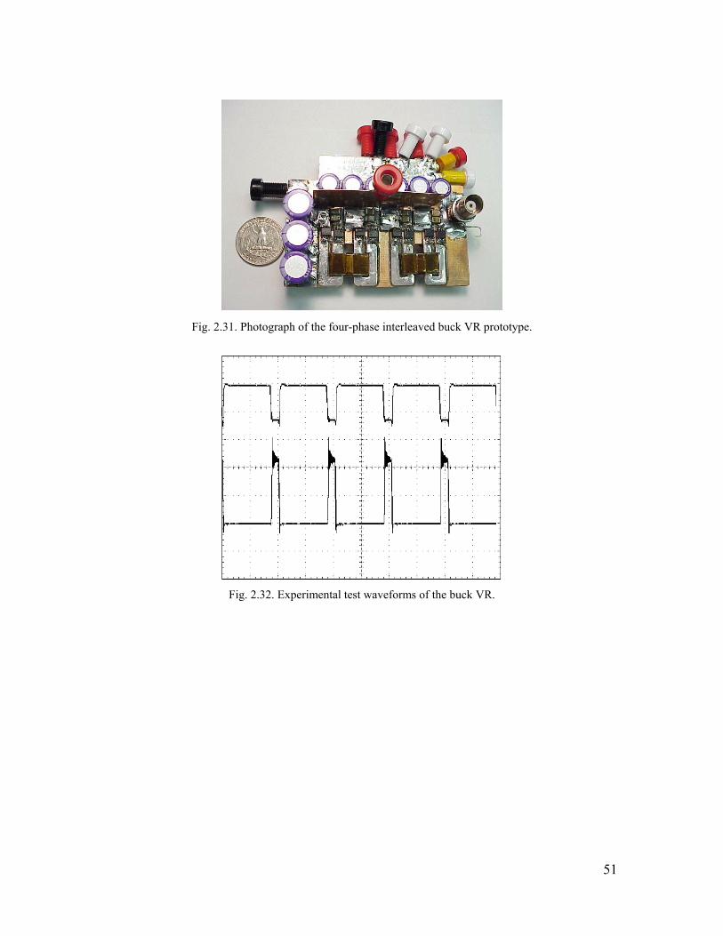
51
Fig. 2.31. Photograph of the four-phase interleaved buck VR prototype.
Fig. 2.32. Experimental test waveforms of the buck VR.
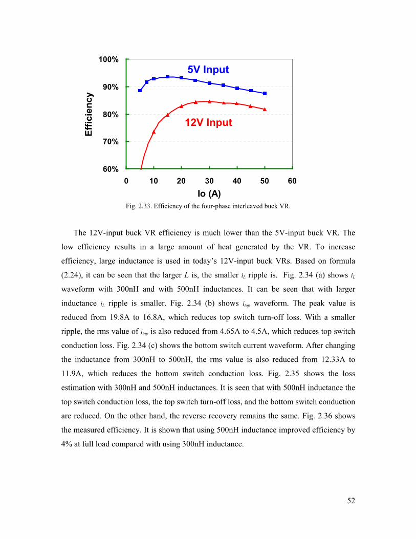
52
60%
70%
80%
90%
100%
0 10 20 30 40 50 60Io (A)
Effic
ienc
y
5V Input
12V Input
Fig. 2.33. Efficiency of the four-phase interleaved buck VR.
The 12V-input buck VR efficiency is much lower than the 5V-input buck VR. The
low efficiency results in a large amount of heat generated by the VR. To increase
efficiency, large inductance is used in today’s 12V-input buck VRs. Based on formula
(2.24), it can be seen that the larger L is, the smaller iL ripple is. Fig. 2.34 (a) shows iL
waveform with 300nH and with 500nH inductances. It can be seen that with larger
inductance iL ripple is smaller. Fig. 2.34 (b) shows itop waveform. The peak value is
reduced from 19.8A to 16.8A, which reduces top switch turn-off loss. With a smaller
ripple, the rms value of itop is also reduced from 4.65A to 4.5A, which reduces top switch
conduction loss. Fig. 2.34 (c) shows the bottom switch current waveform. After changing
the inductance from 300nH to 500nH, the rms value is also reduced from 12.33A to
11.9A, which reduces the bottom switch conduction loss. Fig. 2.35 shows the loss
estimation with 300nH and 500nH inductances. It is seen that with 500nH inductance the
top switch conduction loss, the top switch turn-off loss, and the bottom switch conduction
are reduced. On the other hand, the reverse recovery remains the same. Fig. 2.36 shows
the measured efficiency. It is shown that using 500nH inductance improved efficiency by
4% at full load compared with using 300nH inductance.
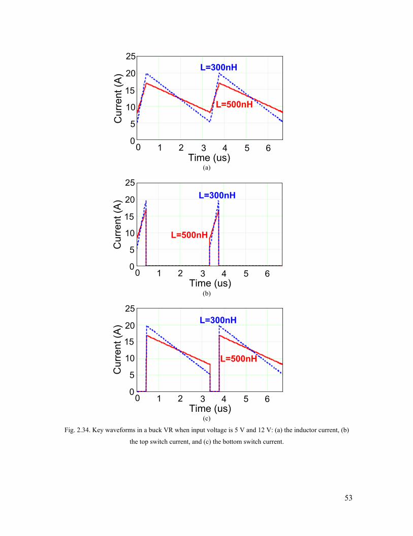
53
25
20
15
10
5
01 20 3 4 5 6
Time (us)
Cur
rent
(A)
L=500nH
L=300nH
(a)
25
20
15
10
5
01 20 3 4 5 6
Time (us)
Cur
rent
(A)
L=500nH
L=300nH
(b)
25
20
15
10
5
01 20 3 4 5 6
Time (us)
Cur
rent
(A)
L=500nH
L=300nH
(c)
Fig. 2.34. Key waveforms in a buck VR when input voltage is 5 V and 12 V: (a) the inductor current, (b)
the top switch current, and (c) the bottom switch current.
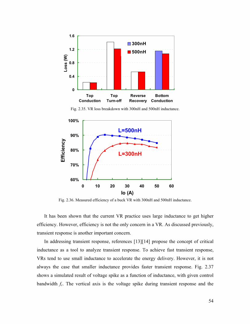
54
0
0.4
0.8
1.2
1.6
TopConduction
TopTurn-off
ReverseRecovery
BottomConduction
Loss
(W)
300nH
500nH
Fig. 2.35. VR loss breakdown with 300nH and 500nH inductance.
60%
70%
80%
90%
100%
0 10 20 30 40 50 60Io (A)
Effic
ienc
y
L=500nH
L=300nH
Fig. 2.36. Measured efficiency of a buck VR with 300nH and 500nH inductance.
It has been shown that the current VR practice uses large inductance to get higher
efficiency. However, efficiency is not the only concern in a VR. As discussed previously,
transient response is another important concern.
In addressing transient response, references [13][14] propose the concept of critical
inductance as a tool to analyze transient response. To achieve fast transient response,
VRs tend to use small inductance to accelerate the energy delivery. However, it is not
always the case that smaller inductance provides faster transient response. Fig. 2.37
shows a simulated result of voltage spike as a function of inductance, with given control
bandwidth fc. The vertical axis is the voltage spike during transient response and the
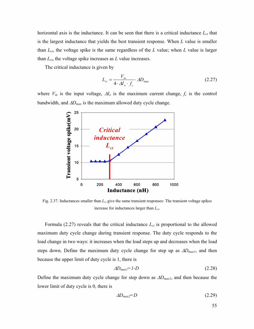
55
horizontal axis is the inductance. It can be seen that there is a critical inductance Lct that
is the largest inductance that yields the best transient response. When L value is smaller
than Lct, the voltage spike is the same regardless of the L value; when L value is larger
than Lct, the voltage spike increases as L value increases.
The critical inductance is given by
max4D
fIV
Lco
inct ∆
∆⋅
⋅⋅= (2.27)
where Vin is the input voltage, ∆Io is the maximum current change, fc is the control
bandwidth, and ∆Dmax is the maximum allowed duty cycle change.
5
10
15
20
25
0 200 400 600 800 1000
Tra
nsie
nt v
olta
ge sp
ike(
mV
)
Inductance (nH)
Critical inductance
Lct
5
10
15
20
25
0 200 400 600 800 1000
Tra
nsie
nt v
olta
ge sp
ike(
mV
)
Inductance (nH)
Critical inductance
Lct
Fig. 2.37. Inductances smaller than Lct give the same transient responses: The transient voltage spikes
increase for inductances larger than Lct.
Formula (2.27) reveals that the critical inductance Lct is proportional to the allowed
maximum duty cycle change during transient response. The duty cycle responds to the
load change in two ways: it increases when the load steps up and decreases when the load
steps down. Define the maximum duty cycle change for step up as ∆Dmax1, and then
because the upper limit of duty cycle is 1, there is
∆Dmax1=1-D (2.28)
Define the maximum duty cycle change for step down as ∆Dmax2, and then because the
lower limit of duty cycle is 0, there is
∆Dmax2=D (2.29)
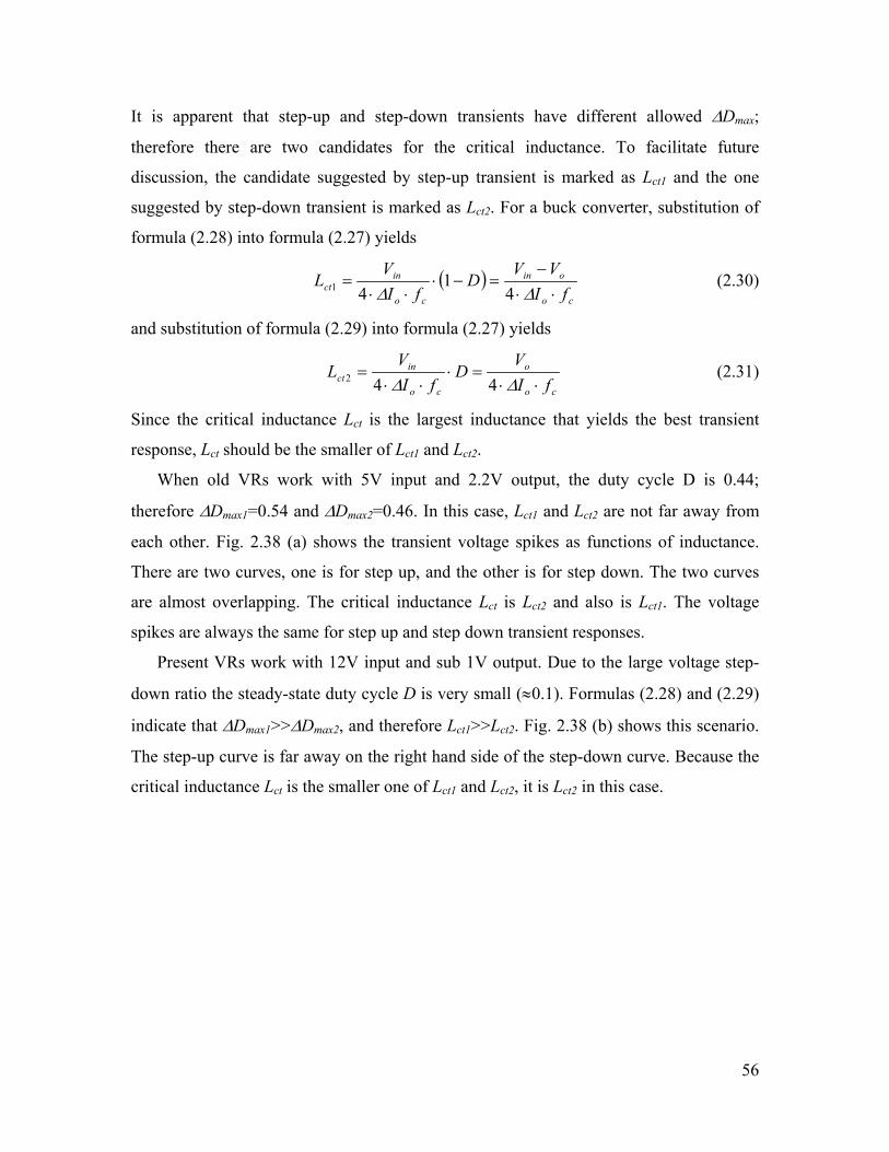
56
It is apparent that step-up and step-down transients have different allowed ∆Dmax;
therefore there are two candidates for the critical inductance. To facilitate future
discussion, the candidate suggested by step-up transient is marked as Lct1 and the one
suggested by step-down transient is marked as Lct2. For a buck converter, substitution of
formula (2.28) into formula (2.27) yields
( )co
oin
co
inct fI
VVD
fIV
L⋅⋅
−=−⋅
⋅⋅=
∆∆ 41
41 (2.30)
and substitution of formula (2.29) into formula (2.27) yields
co
o
co
inct fI
VD
fIV
L⋅⋅
=⋅⋅⋅
=∆∆ 442 (2.31)
Since the critical inductance Lct is the largest inductance that yields the best transient
response, Lct should be the smaller of Lct1 and Lct2.
When old VRs work with 5V input and 2.2V output, the duty cycle D is 0.44;
therefore ∆Dmax1=0.54 and ∆Dmax2=0.46. In this case, Lct1 and Lct2 are not far away from
each other. Fig. 2.38 (a) shows the transient voltage spikes as functions of inductance.
There are two curves, one is for step up, and the other is for step down. The two curves
are almost overlapping. The critical inductance Lct is Lct2 and also is Lct1. The voltage
spikes are always the same for step up and step down transient responses.
Present VRs work with 12V input and sub 1V output. Due to the large voltage step-
down ratio the steady-state duty cycle D is very small (≈0.1). Formulas (2.28) and (2.29)
indicate that ∆Dmax1>>∆Dmax2, and therefore Lct1>>Lct2. Fig. 2.38 (b) shows this scenario.
The step-up curve is far away on the right hand side of the step-down curve. Because the
critical inductance Lct is the smaller one of Lct1 and Lct2, it is Lct2 in this case.
57
Lct
L
∆Vo
∆Vmin
step down
step up
Lct2 Lct1
Vin=5V
(a)
L
∆Vo
∆Vmin
step down
step up
Lct2 Lct1Lct
Vin=12V
(b)
Fig. 2.38. The relationship of inductance L and transient voltage spike ∆Vo: (a) for 5V-input buck VRs,
and (b) for 12V-input VRs.

58
In the current 12V-input VR approach, the inductance is larger than the critical
inductance in order to maximize VR efficiency. For example: for Vo=1.5V, ∆Io=12.5A
(per phase), fc=100KHz, the critical inductance is Lct=300nH. However, the normal
practice of a commercial VR is around 500 ~ 1000nH range. Fig. 2.39 shows the transient
voltage spikes vs. inductance with fixed control bandwidth fc and amount of output
ceramic capacitance Co. Fig. 2.40 (a) shows the simulated transient voltage spikes when
the real L value is equal to Lct. It can be seen that step up and step down create same
transient voltage spikes. Fig. 2.40 (b) shows the simulated transient voltage spikes when
the real L value is larger than Lct. It can be seen that step up creates a larger transient
voltage spike than step down.
Using large inductance increases the step-down voltage spike. To maintain the same
voltage spike magnitude, more capacitance is needed. Fig. 2.41 shows the simulation
result of the transient voltage spike. After more capacitance is used, the transient voltage
is reduced. This is the penalty of the large inductance used. The VR efficiency is
increased, but the output capacitor size and cost are increased too.
L
∆Vo
∆Vmin
step down
step up
Lct2 Lct1
300nH300nH 500nH500nH
Lct Fig. 2.39. Inductance impact on transient voltage spikes.

59
L=Lct
Vo
(a)
L>Lct
Vo
(b)
Fig. 2.40. Simulated transient voltage spikes: (a) For 5V-input VRs, and (b) for 12V-input VRs.
L>Lct
Vo
L>Lct
Vo
Fig. 2.41. Simulated transient voltage spikes with more output capacitors.
In today’s VR design, adaptive voltage positioning (AVP) is a requirement for VR
output voltage. Fig. 2.42 (a) shows the AVP design when the real L value is equal to Lct.
The first waveform is the load current io. The second waveform is the output voltage Vo
without AVP; step down and step up creates same magnitude of voltage spikes. The third
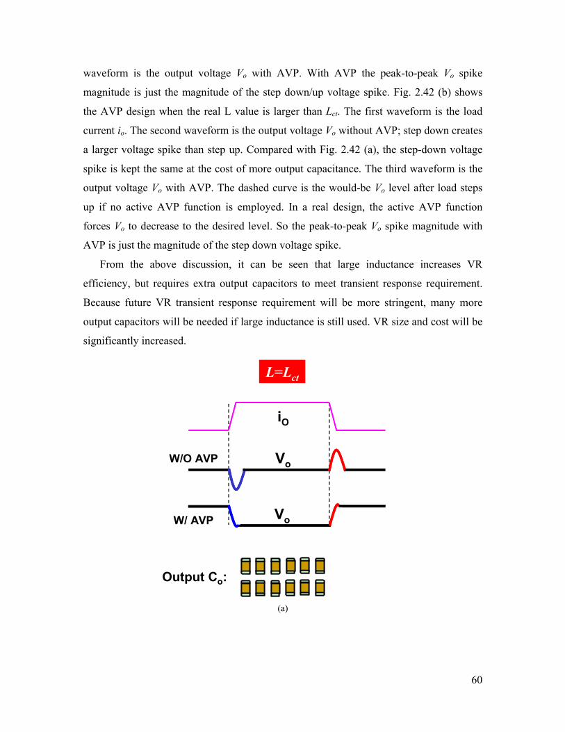
60
waveform is the output voltage Vo with AVP. With AVP the peak-to-peak Vo spike
magnitude is just the magnitude of the step down/up voltage spike. Fig. 2.42 (b) shows
the AVP design when the real L value is larger than Lct. The first waveform is the load
current io. The second waveform is the output voltage Vo without AVP; step down creates
a larger voltage spike than step up. Compared with Fig. 2.42 (a), the step-down voltage
spike is kept the same at the cost of more output capacitance. The third waveform is the
output voltage Vo with AVP. The dashed curve is the would-be Vo level after load steps
up if no active AVP function is employed. In a real design, the active AVP function
forces Vo to decrease to the desired level. So the peak-to-peak Vo spike magnitude with
AVP is just the magnitude of the step down voltage spike.
From the above discussion, it can be seen that large inductance increases VR
efficiency, but requires extra output capacitors to meet transient response requirement.
Because future VR transient response requirement will be more stringent, many more
output capacitors will be needed if large inductance is still used. VR size and cost will be
significantly increased.
iO
W/O AVP Vo
W/ AVP Vo
L=Lct
Output Co:
(a)
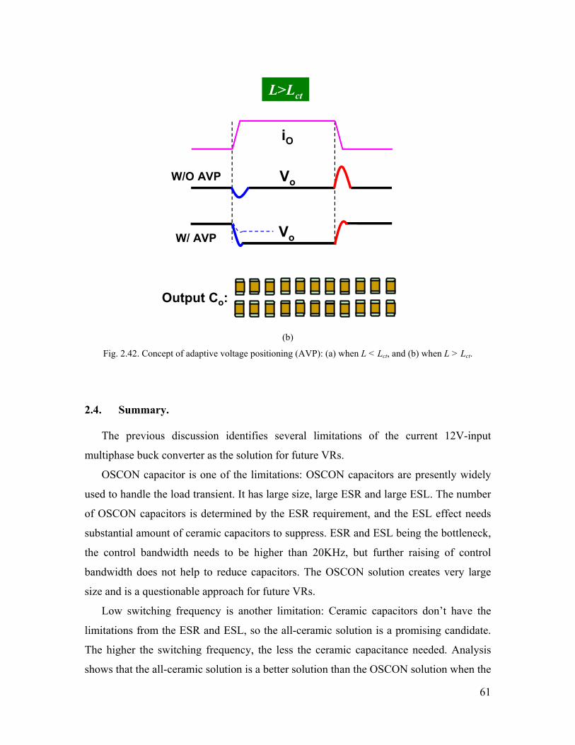
61
W/O AVP Vo
W/ AVP Vo
iO
L>Lct
Output Co:
(b)
Fig. 2.42. Concept of adaptive voltage positioning (AVP): (a) when L < Lct, and (b) when L > Lct.
2.4. Summary.
The previous discussion identifies several limitations of the current 12V-input
multiphase buck converter as the solution for future VRs.
OSCON capacitor is one of the limitations: OSCON capacitors are presently widely
used to handle the load transient. It has large size, large ESR and large ESL. The number
of OSCON capacitors is determined by the ESR requirement, and the ESL effect needs
substantial amount of ceramic capacitors to suppress. ESR and ESL being the bottleneck,
the control bandwidth needs to be higher than 20KHz, but further raising of control
bandwidth does not help to reduce capacitors. The OSCON solution creates very large
size and is a questionable approach for future VRs.
Low switching frequency is another limitation: Ceramic capacitors don’t have the
limitations from the ESR and ESL, so the all-ceramic solution is a promising candidate.
The higher the switching frequency, the less the ceramic capacitance needed. Analysis
shows that the all-ceramic solution is a better solution than the OSCON solution when the

62
VR switching frequency exceeds a certain value, which is approximately 1MHz.
However, 12V-input multiphase buck converter suffers low efficiency at high switching
frequency, which rules out a legitimate chance for the current VR topology to benefit
from high switching frequency. Therefore the current VRs switch at low frequency,
which results in large VR size.
The large inductance is also a limitation. After VR input voltage changes from 5V to
12V, VR efficiency suffers due to the extreme duty cycle. Large inductance is used in the
buck converter to reduce the switching loss and the conduction loss; therefore decent
efficiency is achieved. But because the inductance used is larger than the critical
inductance, the transient response gets worse. More output capacitors are needed to
handle the load transient. This approach will require many more output capacitors for the
future, which is bulky and costly.
A new VR solution is needed. The new VR solution needs to
(1) use all-ceramic output capacitors to avoid the limitations of large ESR and ESL;
(2) use the critical inductance as the L value to minimize the output capacitors;
(3) have high efficiency at high switching frequency.
63
Chapter 3. Innovative Topological Approach to Extend Duty Cycle
The Push-Pull Buck (PPB) Converter
3.1. Benefits of Extending Duty Cycle.
At the end of last chapter, the three features of future VRs are identified. The
technical barriers of using all-ceramic capacitors, using critical inductance, and operating
at high switching frequency all come down to low efficiency. In Chapter 2, it is shown
that high switching frequency can reduce the capacitor size and cost. The all-ceramic
solution is of smaller size and lower cost when the switching frequency reaches 1MHz.
But high switching frequency decreases VR efficiency. Desktop computers are cost
sensitive. This fact places bounds on the effective power removal capabilities of the
chassis, which means high efficiency is a must. Thus the current 12V-input multiphase
buck solution does not benefit from high switching frequency.
In Chapter 2, it is also concluded that the extreme duty cycle in the 12V-input
multiphase buck solution is the main reason of low efficiency. The extreme duty cycle
increases switching loss and reverse recovery loss, which are frequency-related and
increase greatly when VRs work with high switching frequency; therefore VRs suffer low
efficiency. With the 12V-input multiphase buck converter facing great challenges as the
solution for future VRs, a lot of effort has been made in searching for alternatives [15] ~
[29].
Since the extreme duty cycle is the fundamental limitation of current buck VRs, it is a
natural thinking to extend the duty cycle. However, for buck VRs, because the duty cycle
is given byin
oV
VD = , where Vo is the specified output voltage and Vin is the given input
voltage, it cannot be extended. To extend the duty cycle, the buck converter needs to be
modified.
Fig. 3.1 (a) shows a conceptual solution for future VRs. The three desired features are
marked and illustrated: The first one is the output capacitors it uses ceramic
capacitors; the second one is the inductance it uses critical inductance; and the third
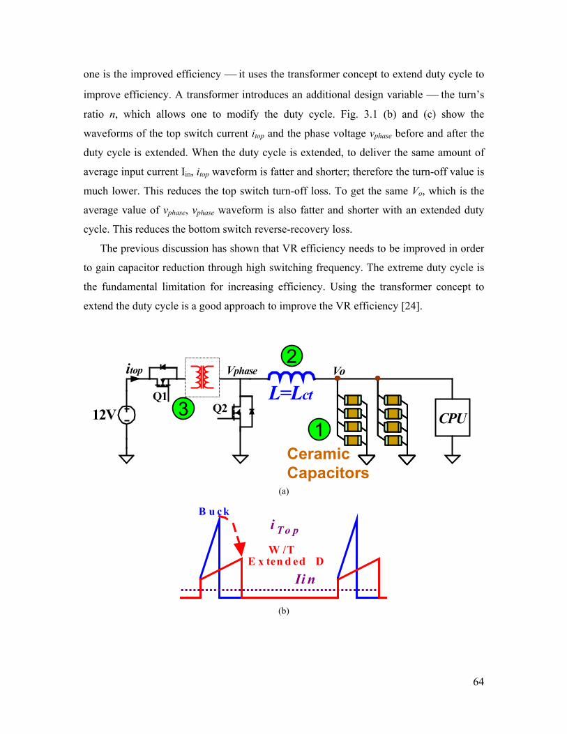
64
one is the improved efficiency it uses the transformer concept to extend duty cycle to
improve efficiency. A transformer introduces an additional design variable the turn’s
ratio n, which allows one to modify the duty cycle. Fig. 3.1 (b) and (c) show the
waveforms of the top switch current itop and the phase voltage vphase before and after the
duty cycle is extended. When the duty cycle is extended, to deliver the same amount of
average input current Iin, itop waveform is fatter and shorter; therefore the turn-off value is
much lower. This reduces the top switch turn-off loss. To get the same Vo, which is the
average value of vphase, vphase waveform is also fatter and shorter with an extended duty
cycle. This reduces the bottom switch reverse-recovery loss.
The previous discussion has shown that VR efficiency needs to be improved in order
to gain capacitor reduction through high switching frequency. The extreme duty cycle is
the fundamental limitation for increasing efficiency. Using the transformer concept to
extend the duty cycle is a good approach to improve the VR efficiency [24].
L=Lct
Vo
12VQ1
Q2
Vphaseitop
CPU
Ceramic Capacitors
1
2
3
(a)
Ii n
i T o p
B u ck
W /TE x ten d ed D
(b)
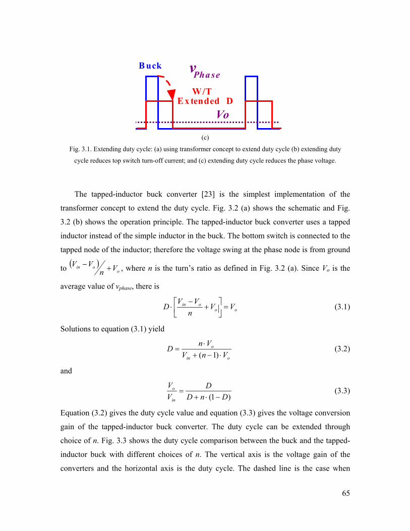
65
Vo
vPha seB uck
W/TEx tended D
(c)
Fig. 3.1. Extending duty cycle: (a) using transformer concept to extend duty cycle (b) extending duty
cycle reduces top switch turn-off current; and (c) extending duty cycle reduces the phase voltage.
The tapped-inductor buck converter [23] is the simplest implementation of the
transformer concept to extend the duty cycle. Fig. 3.2 (a) shows the schematic and Fig.
3.2 (b) shows the operation principle. The tapped-inductor buck converter uses a tapped
inductor instead of the simple inductor in the buck. The bottom switch is connected to the
tapped node of the inductor; therefore the voltage swing at the phase node is from ground
to ( )o
oin VnVV +− , where n is the turn’s ratio as defined in Fig. 3.2 (a). Since Vo is the
average value of vphase, there is
oooin VV
nVV
D =
+
−⋅ (3.1)
Solutions to equation (3.1) yield
oin
o
VnVVn
D⋅−+
⋅=
)1( (3.2)
and
)1( DnDD
VV
in
o
−⋅+= (3.3)
Equation (3.2) gives the duty cycle value and equation (3.3) gives the voltage conversion
gain of the tapped-inductor buck converter. The duty cycle can be extended through
choice of n. Fig. 3.3 shows the duty cycle comparison between the buck and the tapped-
inductor buck with different choices of n. The vertical axis is the voltage gain of the
converters and the horizontal axis is the duty cycle. The dashed line is the case when

66
Vin=12V and Vo=1.5V, so the voltage gain is 0.125. A buck converter needs a duty cycle
equal to 0.125 to do the conversion; a tapped-inductor buck converter with n=2 needs a
duty cycle equal to 0.222 to do the conversion; a tapped-inductor buck converter with
n=3 needs a duty cycle equal to 0.3 to do the conversion; etc. The trend is that a larger n
extends the duty cycle more.
Similar to that in a buck converter, the output inductor L is defined as the inductor
between the phase node and the output. Accordingly, the inductance formed by the n-turn
structure is n2L. The inductor of n2L “bucks” Vin-Vo during Q1 conduction. When Q1
turns off, all the energy stored in n2L is transferred to L through magnetic coupling; so the
inductor current iL is jumping, which causes additional switching ripple at Vo. This is one
disadvantage of the tapped-inductor buck converter.
There is another serious issue for the tapped-inductor buck converter: the leakage
inductor associated with the tapped-inductor structure, as marked as Lk in Fig. 3.2 (a).
Since Lk is in series with Q1, when Q1 turns off, the energy stored in Lk causes a voltage
spike across Q1 as the waveform VDS1 in Fig. 3.2 (b) shows. If the energy stored in Lk is
large enough, the voltage spike can be higher than the maximum drain-source voltage
rating of Q1, therefore Q1 is broken down; also that the energy stored in the Lk is purely
dissipated when Q1 turns off is bad from the efficiency point of view.
A four-phase interleaved tapped-inductor buck VR prototype is built. The design
specifications are the same as that of the benchmark buck built in Chapter 2: Vin=12V,
Vo=1.5V, Io=50A, and fs=300KHz/phase. The same devices are used here as in the
benchmark buck converter. The top switches are Si4884DY (30V, Rds=10.5mΩ,
Qgd=4.8nC) and the bottom switches are Si4874DY (30V, Rds=7.5mΩ, Qg=35nC). Fig.
3.4 shows the magnetic structure. Each tapped inductor consists of a two-turn structure
and the drain of the bottom device is connected to the middle node of the two turns. The
output inductor value L is designed equal to 300nH, which is also the inductance used in
the benchmark buck converter.
In Fig. 3.5 is a photograph of the prototype. Experimental test waveforms are given in
Fig. 3.6. From top to bottom, the traces are: the top switch current iQ1; gate signal of the
bottom switch Vgs2; top switch drain-source voltage VDS1; and bottom switch drain-source
voltage VDS2. It is seen that with extended duty cycle, iQ1 waveform is extended, which
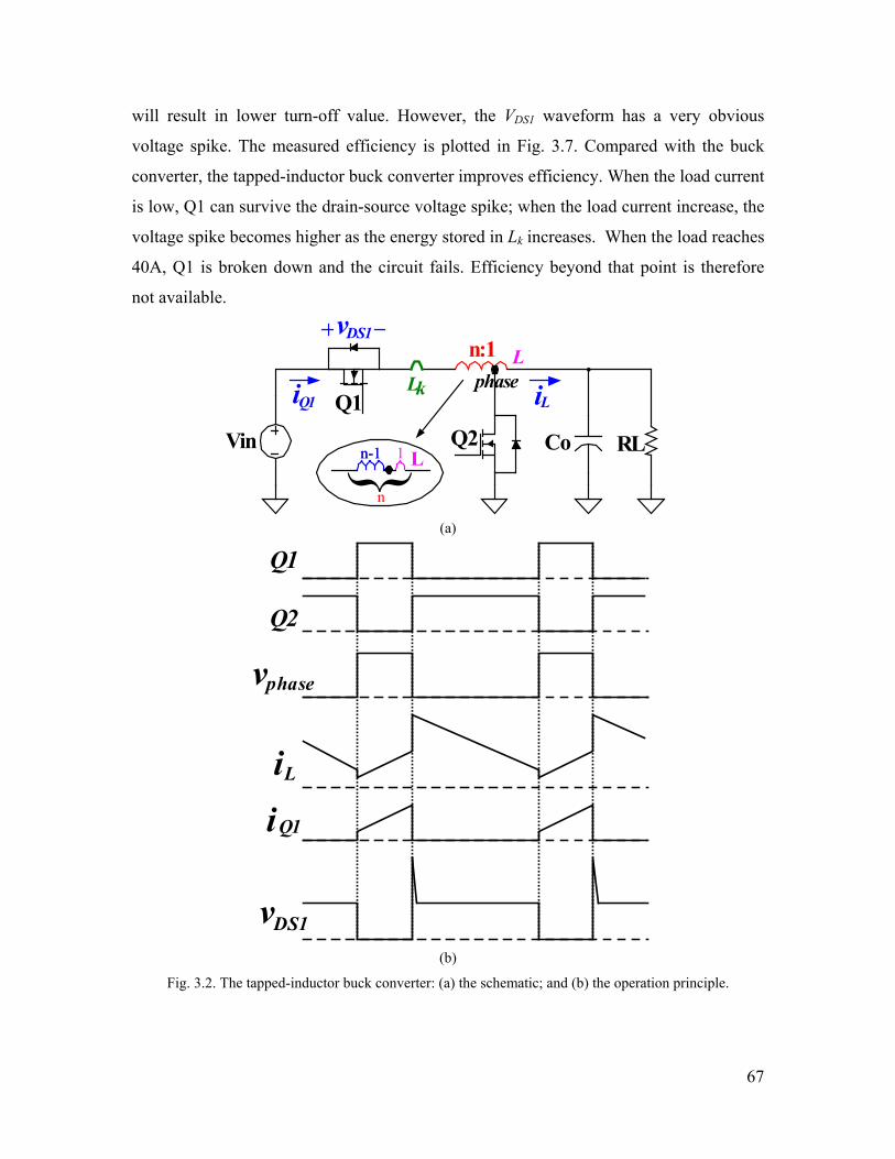
67
will result in lower turn-off value. However, the VDS1 waveform has a very obvious
voltage spike. The measured efficiency is plotted in Fig. 3.7. Compared with the buck
converter, the tapped-inductor buck converter improves efficiency. When the load current
is low, Q1 can survive the drain-source voltage spike; when the load current increase, the
voltage spike becomes higher as the energy stored in Lk increases. When the load reaches
40A, Q1 is broken down and the circuit fails. Efficiency beyond that point is therefore
not available.
Co RLVin Q2Q1
n:1
iL
phase
n-1 1
n
n-1 LL
LkiQ1
vDS1
(a)
Q1
Q2
iL
Q1i
DS1v
vphase
(b)
Fig. 3.2. The tapped-inductor buck converter: (a) the schematic; and (b) the operation principle.
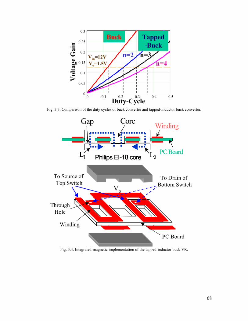
68
0 0.1 0.2 0.3 0.4 0.50
0.05
0.1
0.15
0.2
0.25
0.3
Buck Tapped-Buck
n=2 n=3n=4
Vin=12VVo=1.5V
Duty-Cycle
Vol
tage
Gai
n
Fig. 3.3. Comparison of the duty cycles of buck converter and tapped-inductor buck converter.
Core Winding
PC Board
Gap
Philips EI-18 coreL1 L2
Core Winding
PC Board
Gap
Philips EI-18 coreL1 L2
PC Board
Winding
Through Hole
To Source of Top Switch
Vo
To Drain of Bottom Switch
Fig. 3.4. Integrated-magnetic implementation of the tapped-inductor buck VR.
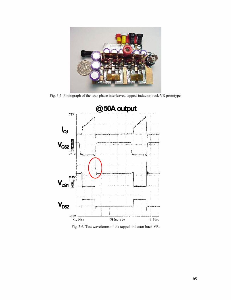
69
Fig. 3.5. Photograph of the four-phase interleaved tapped-inductor buck VR prototype.
@ 50A output
VGS2
VDS1
VDS2
IQ1
@ 50A output
VGS2
VDS1
VDS2
IQ1
VGS2
VDS1
VDS2
IQ1
Fig. 3.6. Test waveforms of the tapped-inductor buck VR.
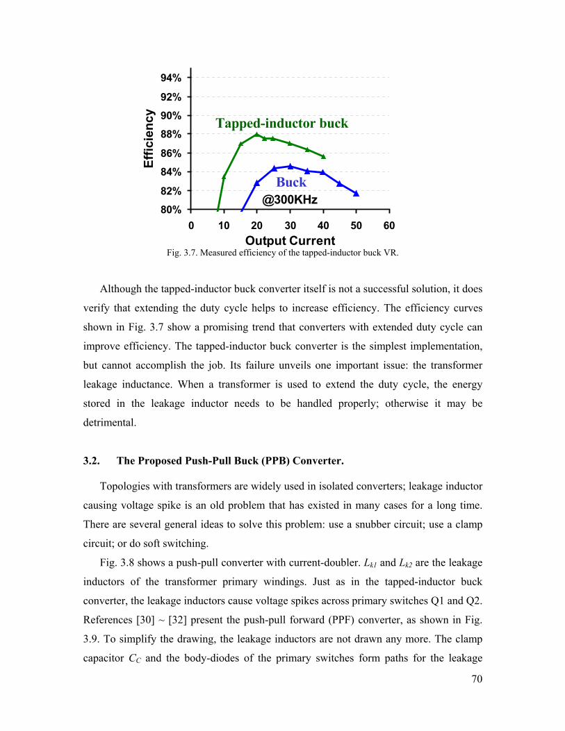
70
80%
82%
84%
86%
88%
90%
92%
94%
0 10 20 30 40 50 60Output Current
Effic
ienc
y
Tapped-inductor buck
Buck@300KHz
Fig. 3.7. Measured efficiency of the tapped-inductor buck VR.
Although the tapped-inductor buck converter itself is not a successful solution, it does
verify that extending the duty cycle helps to increase efficiency. The efficiency curves
shown in Fig. 3.7 show a promising trend that converters with extended duty cycle can
improve efficiency. The tapped-inductor buck converter is the simplest implementation,
but cannot accomplish the job. Its failure unveils one important issue: the transformer
leakage inductance. When a transformer is used to extend the duty cycle, the energy
stored in the leakage inductor needs to be handled properly; otherwise it may be
detrimental.
3.2. The Proposed Push-Pull Buck (PPB) Converter.
Topologies with transformers are widely used in isolated converters; leakage inductor
causing voltage spike is an old problem that has existed in many cases for a long time.
There are several general ideas to solve this problem: use a snubber circuit; use a clamp
circuit; or do soft switching.
Fig. 3.8 shows a push-pull converter with current-doubler. Lk1 and Lk2 are the leakage
inductors of the transformer primary windings. Just as in the tapped-inductor buck
converter, the leakage inductors cause voltage spikes across primary switches Q1 and Q2.
References [30] ~ [32] present the push-pull forward (PPF) converter, as shown in Fig.
3.9. To simplify the drawing, the leakage inductors are not drawn any more. The clamp
capacitor CC and the body-diodes of the primary switches form paths for the leakage

71
inductor currents to flow during the primary switches off period. This simple concept
helps to clamp the voltage spike across the primary switches at CC voltage. In addition,
the energy stored in the leakage inductors is recovered, which helps to increase
efficiency.
Co RL
Q2
Q4
Vo
L
L
1 *
Vin
Q1
n
*
Q3 *n
k1L
k2L
Fig. 3.8. The push-pull converter with current doubler.
Co RL
Q2
Q4
Vo
L
L
1 *
Vin
Q1
Q3
n
*
*n
Cc
iQ1
Fig. 3.9. The push-pull forward converter with current doubler.
The PPF converter is developed for 48V-input transformer-isolated VR application.
The clamp method is developed to solve problem caused by the transformer leakage
inductors. However, after the transformer concept is plugged in, the non-isolated VR in
nature greatly resembles the isolated VR, although the transformer is not used as an
isolation method. Therefore the solutions developed for isolated converters can be
applied to the non-isolated VR with some minimum modification.
The PPF converter is a success for 48-input isolated VR; this motivates one to modify
it to fit in the non-isolated VR application. The most straightforward modification is to
connect the primary and secondary grounds together. But that’s just a non-isolated PPF
converter.
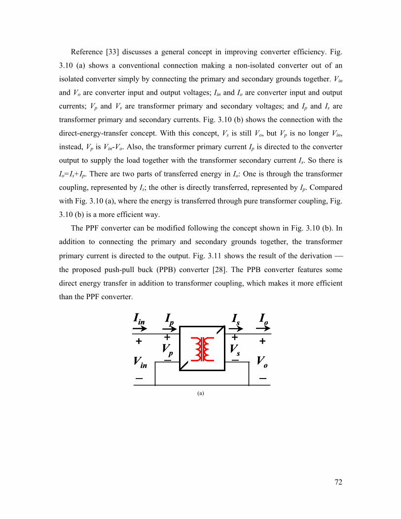
72
Reference [33] discusses a general concept in improving converter efficiency. Fig.
3.10 (a) shows a conventional connection making a non-isolated converter out of an
isolated converter simply by connecting the primary and secondary grounds together. Vin
and Vo are converter input and output voltages; Iin and Io are converter input and output
currents; Vp and Vs are transformer primary and secondary voltages; and Ip and Is are
transformer primary and secondary currents. Fig. 3.10 (b) shows the connection with the
direct-energy-transfer concept. With this concept, Vs is still Vo, but Vp is no longer Vin,
instead, Vp is Vin-Vo. Also, the transformer primary current Ip is directed to the converter
output to supply the load together with the transformer secondary current Is. So there is
Io=Is+Ip. There are two parts of transferred energy in Io: One is through the transformer
coupling, represented by Is; the other is directly transferred, represented by Ip. Compared
with Fig. 3.10 (a), where the energy is transferred through pure transformer coupling, Fig.
3.10 (b) is a more efficient way.
The PPF converter can be modified following the concept shown in Fig. 3.10 (b). In
addition to connecting the primary and secondary grounds together, the transformer
primary current is directed to the output. Fig. 3.11 shows the result of the derivation
the proposed push-pull buck (PPB) converter [28]. The PPB converter features some
direct energy transfer in addition to transformer coupling, which makes it more efficient
than the PPF converter.
Vin
Iin
Vo
Io
+
_
+
_
Ip
+_
Is
Vp Vs
+_Vin
Iin
Vo
Io
+
_
+
_
Ip
+_
Is
Vp Vs
+_
(a)

73
Vin
Iin
Vo
Io
+
_
+
_
Ip
+_
Is
Vp Vs
+_
(b)
Fig. 3.10. A general concept of direct energy transfer: (a) Conventional connection, and (b) with the
direct-energy-transfer concept.
Co RL
Q2
Q4
Vo
L
L
1 *
Vin
Q1
Q3
n
*
*n
CciL1
iQ1
vDS1"Phase 1"
"Phase 2"
iL2
vDS3
iQ3
vCc
Fig. 3.11. The proposed push-pull buck (PPB) converter with current doubler.
Fig. 3.12 shows the operation principle of the PPB converter. The transformer turns
ratio is n:1.
VCc is the voltage across the clamp capacitor Cc. Because the transformer primary
windings cannot sustain DC voltage, VCc is Vin-Vo.
During t1~t2 Q1 is on, Q2 is off and Q4 is on for inductor L2 current freewheeling; the
converter is in the energy transfer mode. Fig. 3.13 (a) shows the equivalent circuit. The
voltage applied to both primary windings is Vin-Vo. Through transfer coupling, “phase 1”
voltage potential is ( )n
VV oin − , thus the inductor L1 current iL1 is charged up. In the
meantime, the transformer primary winding current i1 directly goes to the output as well.
During t2~t3 is the reset of leakage inductor current. Fig. 3.13 (b) shows the
equivalent circuit. Q1 has just been turned off. The leakage inductor Lk1 current has to
continue flowing, so it goes through the body diode of Q3 and the clamp capacitor CC to

74
form a path. In the meantime, the leakage inductor Lk2 current also finds a path through
body diode of Q3 to go the Vin. By doing so the voltage across Q1 is clamped at Vin-Vo. In
this mode, i1 linearly decreases; i2, originally negative, linearly decreases to zero and then
linearly increases. When i1= i2, this mode ends.
During t3~t4 is the freewheeling mode. Fig. 3.13 (c) shows the equivalent circuit. Q2
and Q4 are “on” to provide freewheeling paths for output inductor currents. Transformer
primary currents i1=i2 and go through CC to the output. Note that the transformer primary
windings are in anti-series now, therefore the transformer secondary winding doesn’t
carry any load current. Also because VCc=Vin-Vo, the leakage inductors do not see any
voltage-second so their currents remain constant.
Since t4~t5 is the dual mode of t1~t2, t5~t6 is the dual mode of t2~t3, and t6~t7 is the
dual mode of t3~t4, these are not discussed.
In view of the fact that Vo is the average value of vphase, there is
ooin V
nVV
D =−
⋅ (3.4)
where D is defined as
sTTD 1= (3.5)
in which T1 is the duration of mode t1~t2 and Ts is the duration of a full switching cycle.
Solutions to equation (3.4) yield
oin
o
VVVn
D−⋅
= (3.6)
and
nDD
VV
in
o
+= (3.7)
Formula (3.6) shows that the duty cycle can be extended through choices of a large n. A
design example: Vin=12V, Vo=1.5V, n=2, will yield D=0.286.

75
Q1Q3
iL1
Q1i
vphase1
Q1Q2Q4Q4
Q2Q2Q3 Q3
vphase2
iL2
DS3v
t1 t2 t3 t4 t5 t6 t7
1i
2iini
Q3i
DS1v
Q2i
Q4i
Fig. 3.12. The operation principle of the proposed Push-Pull Buck (PPB) converter.
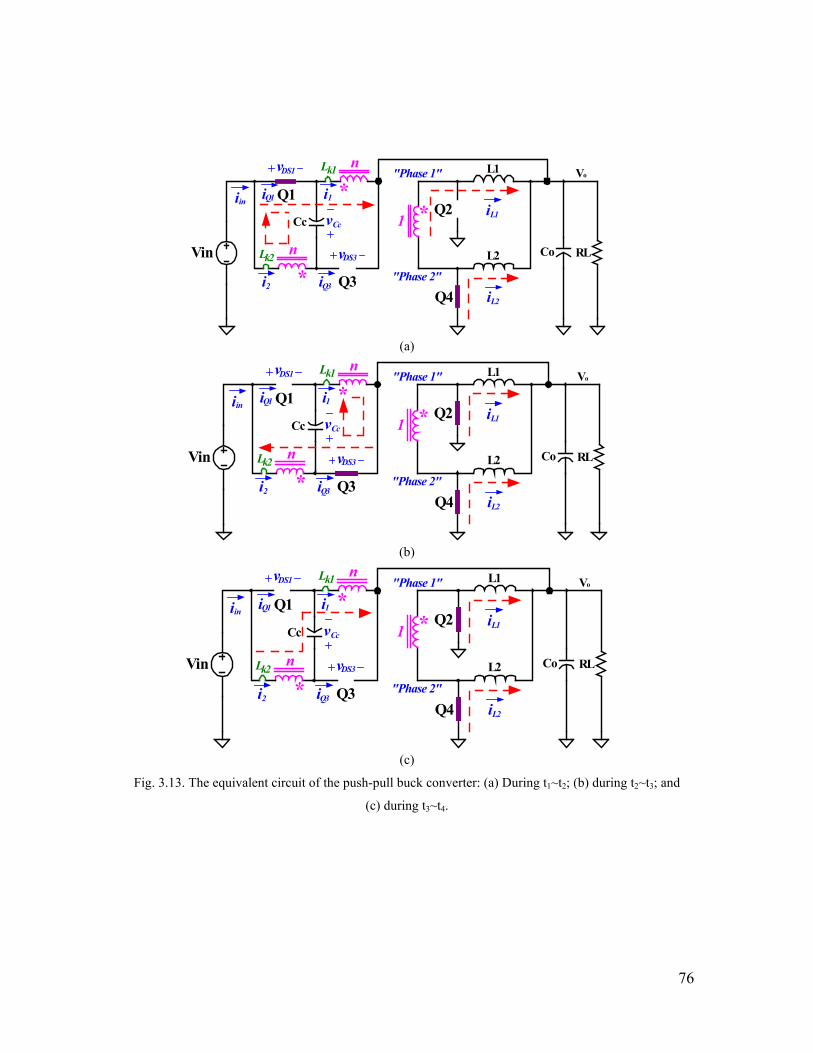
76
Co RL
VoL1
L2
1 *
Vin
n
*
*n
CciL1
iQ1
vDS1 "Phase 1"
"Phase 2"
iL2
vDS3
iQ3
Q1
Q3
Q2
Q4
vCc
k1L
k2L
i1
i2
iin
(a)
Co RL
VoL1
L2
1 *
Vin
n
*
*n
CciL1
iQ1
vDS1 "Phase 1"
"Phase 2"
iL2
vDS3
iQ3
Q1
Q3
Q2
Q4
vCc
k1L
k2L
i1
i2
iin
(b)
Co RL
VoL1
L2
1 *
Vin
n
*
*n
CciL1
iQ1
vDS1 "Phase 1"
"Phase 2"
iL2
vDS3
iQ3
Q1
Q3
Q2
Q4
vCc
k1L
k2L
i1
i2
iin
(c)
Fig. 3.13. The equivalent circuit of the push-pull buck converter: (a) During t1~t2; (b) during t2~t3; and
(c) during t3~t4.

77
Fig. 3.14 (a) shows the comparison of the key waveforms of the PPB converter and
the PPF converter. In both converters, Vin=12V, Vo=1.5V, n=2, fs=300KHz, L=300nH,
and Io=25A. From top to bottom, the waveforms are: top switch current itop, bottom
switch current ibottom, and the phase voltage vphase. The PPF converter waveforms are
shown in dotted lines, and the PPB converter waveforms are shown in solid lines. The
turn-off value of itop is 8.5A in the PPB converter as opposed to 9.8A in the PPF
converter, which helps to reduce the top switch turn-off loss in the PPB converter. The
rms value of ibottom is 14A in the PPB converter, as opposed to 16A in the PPF converter,
which helps to reduce the bottom switch conduction loss in the PPB converter. The peak
value of vphase is 5.25V in the PPB converter, as opposed to 6V in the PPF converter,
which helps to reduce the bottom switch reverse-recovery loss in the PPB converter.
From this example, it is shown that the PPB converter is more efficient than the PPF
converter. The advantage of the PPB converter comes from the direct energy transfer.
Fig. 3.14 (b) shows the comparison of the key waveforms of the PPB converter and
the two-phase buck converter. In both converters, Vin=12V, Vo=1.5V, fs=300KHz,
L=300nH, and Io=25A. The transformer turn’s ratio is n=2 in the PPB converter. From
top to bottom, the waveforms are: top switch current itop, bottom switch current ibottom,
and the phase voltage vphase. The buck converter waveforms are shown as dotted lines,
and the PPB converter waveforms are shown as solid lines. The turn-off value of itop is
8.5A in the PPB converter as opposed to 20.2A in the buck converter, which helps to
substantially reduce the top switch turn-off loss. The rms value of ibottom is 14A in the
PPB converter as opposed to 11.2A in the buck converter, which increases the bottom
switch conduction loss a little bit. The peak value of vphase is 5.25V in the PPB converter
as opposed to 12V in the buck converter, which helps to greatly reduce the bottom switch
reverse-recovery loss.
Fig. 3.15 shows the loss comparison between the PPB converter (n=2) and the two-
phase buck converter. In both converters, the top switches are Si4884DY (30V,
Rds=10.5mΩ, Qgd=4.8nC) and the bottom switches are Si4874DY (30V, Rds=7.5mΩ,
Qg=35nC). From Fig. 3.15 it can be observed that with an extended duty cycle the PPB
converter is able to substantially reduce the top switch turn-off loss and the reverse

78
recovery loss. Meanwhile the PPB converter has larger conduction than the buck
converter. The net result is that the PPB converter has less loss than the buck converter.
PPBPPFitop
ibottom
vphase
(a)
PPB
Buckitop
ibottom
vphase
(b)
Fig. 3.14. Comparison of the key waveforms of: (a) The PPB and the PPB converters; and (b) the PPB
converter and the buck converters.

79
00.5
11.5
22.5
33.5
TopConduction
Top turn off ReverseRecovery
BottomConduction
Loss
(W)
Buck PPB
Fig. 3.15. Loss comparison of the PPB converter and the two-phase buck converter.
3.3. Efficiency Improvement with Integrated Magnetics of the PPB Converter.
The PPB converter uses a current doubler. Three magnetic components are needed,
namely, one transformer and two inductors. In addition to size and cost concerns, the
interconnection loss of these components also negatively impacts the efficiency,
especially in high-current applications [110]. The integrated magnetic (IM) technique can
be used to simplify the magnetic structure. Four IM structures for the PPB converter are
going to be discussed as follows:
Fig. 3.16 (a) shows the schematic associated with IM-1 structure. For a current
doubler, reference [12] proposed a simple way of integrating the transformer and the two
inductors in one core. The structure is shown in Fig. 3.16 (b), marked as IM-1. Primary
windings of the transformer are put around the center leg of the core. There is no air gap
on the center leg. The inductor windings are put on the outer legs of the core. Therefore,
air gaps on both outer legs store energy and form the inductors. The fact that the flux
going through the center leg also goes through the outer legs makes the secondary
winding of the transformer physically unnecessary. The IM-1 structure is simple.
However, it has two disadvantages: the first disadvantage is that because the primary
windings and the secondary windings are on different legs, the coupling is not as good as
when they are on same legs, which means larger leakage inductors; the second
disadvantage is that the AC components of the magnetic flux in the outer legs are added
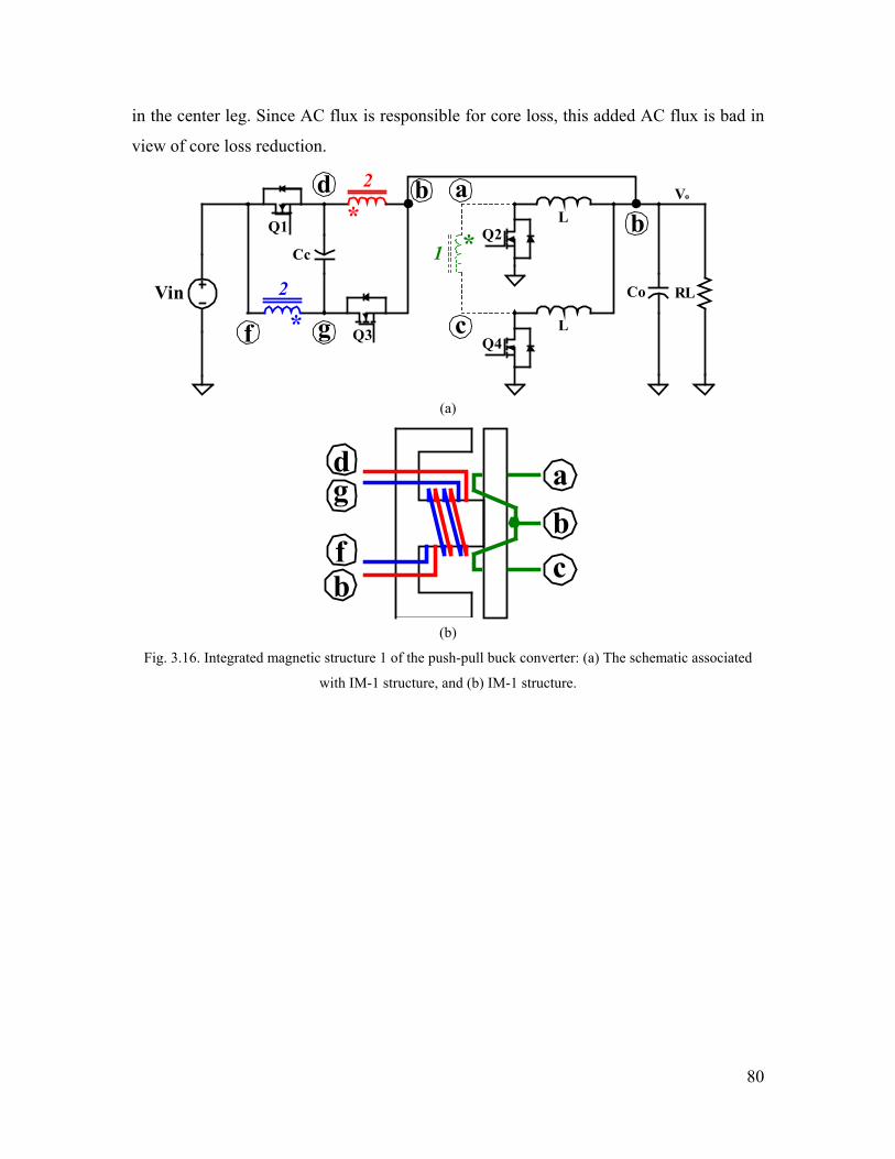
80
in the center leg. Since AC flux is responsible for core loss, this added AC flux is bad in
view of core loss reduction.
Co RL
Q2
Q4
Vo
L
L
1 *
Vin
Q1
Q3
2
*
*2
Cc
d
f g
b a
c
b
(a)
dg
fb
abc
(b)
Fig. 3.16. Integrated magnetic structure 1 of the push-pull buck converter: (a) The schematic associated
with IM-1 structure, and (b) IM-1 structure.
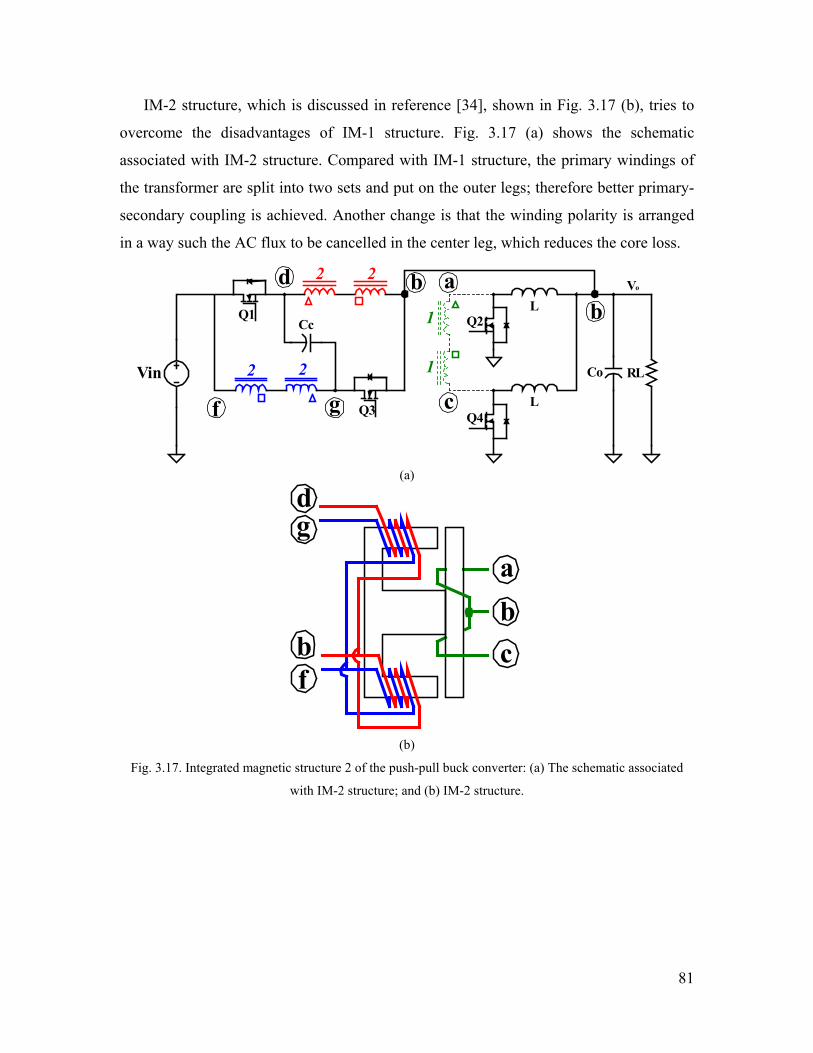
81
IM-2 structure, which is discussed in reference [34], shown in Fig. 3.17 (b), tries to
overcome the disadvantages of IM-1 structure. Fig. 3.17 (a) shows the schematic
associated with IM-2 structure. Compared with IM-1 structure, the primary windings of
the transformer are split into two sets and put on the outer legs; therefore better primary-
secondary coupling is achieved. Another change is that the winding polarity is arranged
in a way such the AC flux to be cancelled in the center leg, which reduces the core loss.
Co RL
Q2
Q4
Vo
L
L
Vin
2
Cc
d
f g
b a
c
b
2
Q3
22
1Q1
1
(a)
dg
fb
abc
(b)
Fig. 3.17. Integrated magnetic structure 2 of the push-pull buck converter: (a) The schematic associated
with IM-2 structure; and (b) IM-2 structure.
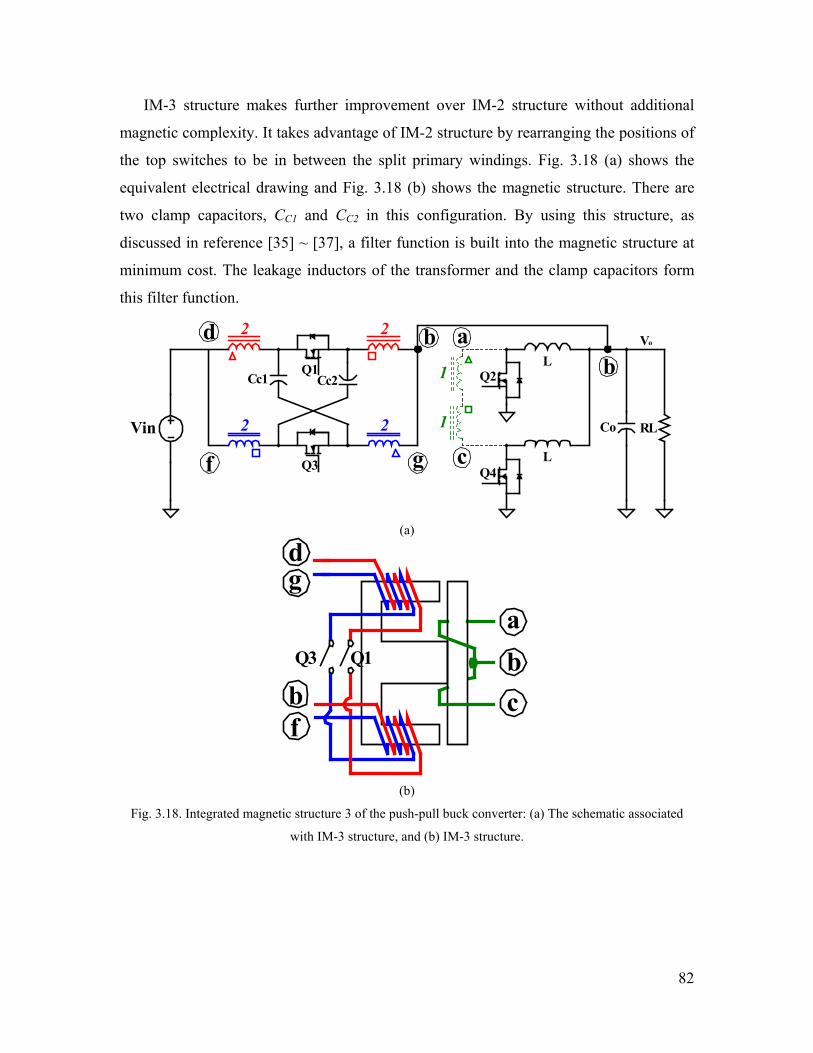
82
IM-3 structure makes further improvement over IM-2 structure without additional
magnetic complexity. It takes advantage of IM-2 structure by rearranging the positions of
the top switches to be in between the split primary windings. Fig. 3.18 (a) shows the
equivalent electrical drawing and Fig. 3.18 (b) shows the magnetic structure. There are
two clamp capacitors, CC1 and CC2 in this configuration. By using this structure, as
discussed in reference [35] ~ [37], a filter function is built into the magnetic structure at
minimum cost. The leakage inductors of the transformer and the clamp capacitors form
this filter function.
Co RL
Q2
Q4
Vo
L
L
Vin
Q1
2
Cc2
d
f g
b a
c
b
2
Q3
22
Cc1 1
1
(a)
dg
fb
abc
Q3 Q1
(b)
Fig. 3.18. Integrated magnetic structure 3 of the push-pull buck converter: (a) The schematic associated
with IM-3 structure, and (b) IM-3 structure.
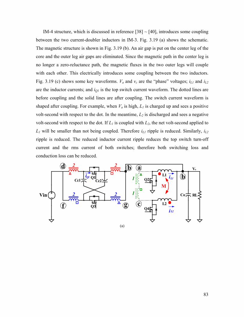
83
IM-4 structure, which is discussed in reference [38] ~ [40], introduces some coupling
between the two current-doubler inductors in IM-3. Fig. 3.19 (a) shows the schematic.
The magnetic structure is shown in Fig. 3.19 (b). An air gap is put on the center leg of the
core and the outer leg air gaps are eliminated. Since the magnetic path in the center leg is
no longer a zero-reluctance path, the magnetic fluxes in the two outer legs will couple
with each other. This electrically introduces some coupling between the two inductors.
Fig. 3.19 (c) shows some key waveforms. Va and vc are the “phase” voltages; iL1 and iL2
are the inductor currents; and iQ1 is the top switch current waveform. The dotted lines are
before coupling and the solid lines are after coupling. The switch current waveform is
shaped after coupling. For example, when Va is high, L1 is charged up and sees a positive
volt-second with respect to the dot. In the meantime, L2 is discharged and sees a negative
volt-second with respect to the dot. If L1 is coupled with L2, the net volt-second applied to
L1 will be smaller than not being coupled. Therefore iL1 ripple is reduced. Similarly, iL2
ripple is reduced. The reduced inductor current ripple reduces the top switch turn-off
current and the rms current of both switches; therefore both switching loss and
conduction loss can be reduced.
Co RL
Q2
Q4
Vo
L1
L2
Vin
Q1
2
Cc2
d
f g
b a
c
b
2
Q3
22
Cc1 1
1M
iL1iQ1
iL2
(a)

84
dg
fb
abc
Q3 Q1
(b)
va
vc
iL1
iL2
D D0.5-D 0.5-D
iQ1
(c)
Fig. 3.19. Integrated magnetic structure 4 of the push-pull buck converter: (a) The schematic associated
with IM-4 structure; (b) IM-4 structure and (c) the current waveforms.
All four IM structures are implemented for comparison when the PPB converter is
prototyped. The four-phase interleaving buck VR prototype built in Chapter 2 is used as a
benchmark. The design specifications are: 12V input, 1.5V output, current load from
0~50A, and 300kHz/phase switching frequency. Devices used in the PPB converter are
85
the same as in the buck converter: The top switches are Si4884DY (30V, Rds=10.5mΩ,
Qgd=4.8nC) and the bottom switches are Si4874DY (30V, Rds=7.5mΩ, Qg=35nC).
The IM structures 1 ~ 4 are implemented with Philips EI-18 planar cores and PCB
windings. The turn’s ratio is n=2. The inductance in the PPB prototypes is the same as
that in the benchmark buck converter: 300nH/phase.
The output capacitor is 6×1200µF OSCON capacitors plus 18×22µF ceramic
capacitors.
Fig. 3.20 (a) shows the IM-1 structure prototype; Fig. 3.20 (b) shows the IM-2
structure prototype; Fig. 3.20 (c) shows the IM-3 structure prototype and Fig. 3.20 (d)
shows the IM-4 structure prototype. Fig. 3.21 shows the experimental test waveforms
from the IM-4 structure PPB prototype. The top two traces are the top switch gate signal
and the bottom switch gate signal. It can be observed that the duty cycle of the PPB
converter is extended compared with the duty cycle of the buck converter shown in Fig.
2.32. The third trace is the top switch drain-source voltage. With the clamp circuit, the
voltage spike caused by the leakage inductor is clamped. The bottom trace is the input
current without an additional input filter. With the integrated filter function in the IM
structure, the input current is smooth.
Fig. 3.22 shows the measured efficiencies of the PPB prototypes and the benchmark
buck converter. It is shown that the PPB converter has higher efficiency than the buck
converter, and that with the progression of the IM structures from 1 to 4, the efficiency of
the PPB converter is increased step by step. IM-4 structure achieves the best efficiency of
the PPB converter. The full-load efficiency is 87.6% and the peak efficiency is 92.1%.
Compared with the buck converter, the efficiency is improved by 6% at full load and the
peak efficiency is improved by 7.5%.

86
(a)
(b)

87
(c)
(d)
Fig. 3.20. IM structure prototypes of the PPB converter: (a) IM-1 structure prototype, (b) IM-2 structure
prototype, (c) IM-3 structure prototype, and (d) IM-4 structure prototype.

88
Top Vds
Input current
Bottom Vgs
Top Vgs
Fig. 3.21. Experimental test waveforms of the PPB converter.
80%
82%
84%
86%
88%
90%
92%
94%
0 10 20 30 40 50 60Output Current
Effic
ienc
y
92.1%
89.0%
84.6%
88.1%
Sync. Buck
IM-1
IM-2IM-4
89.9%IM-3
87.6%
86.2%
81.7%
84.8%85.0%
Fig. 3.22. Measured efficiency comparison of the PPB converter and the buck converter.
3.4. Improved Transient Response of the PPB Converter.
The previous discussion has shown that employing the transformer concept in the
non-isolated VR application can extend the duty cycle and therefore improve efficiency.

89
It is yet to be discussed that what impact extending the duty cycle has on transient
response.
The critical-inductance concept developed in references [13] and [14] is used as a tool
to analyze transient response in the previous chapters. However, the original critical-
inductance concept is for the traditional buck converter. New additions are needed to
address converters with transformers.
Fig. 3.23 (a) shows a schematic drawing. Because the PPB converter is essentially a
two-phase configuration, the load current is denoted as 2Io to make fair comparisons with
the buck converter. Due to the direct energy transfer bypass, the real current that is
injected to the output Vo node not only includes the two output choke inductor currents,
but also includes the directly transferred current. To facilitate the analysis, the two-phase
total output current is denoted as 2iLo. Fig. 3.23 (b) shows an equivalent conceptual
drawing: The PPB converter is considered as a two-phase interleaved structure and each
phase carries current iLo. The inductance of each phase is the real inductance used in the
PPB converter. Therefore iLo stands for a conceptual per-phase inductor current that
supplies energy to the output. This conceptual current is larger than the real current that
flows through the inductor because the directly transferred current is also included in the
conceptual current.
During transient responses, the feedback control generates duty cycle change ∆D to
apply net voltage-second to the inductors, which causes iLo to change up. Reference [106]
includes the small-signal model of the PPB converter, and the average iLo slew rate in
response to ∆D is derived as follows:
nLDV
dtdi in
avg
Lo ∆⋅= (3.8)
From control point of view there is [14]
cLor
Lo
avg
Lo fItI
dtdi
⋅⋅== ∆∆
4 (3.9)
Because formulas (3.8) and (3.9) describe the same fact from two different angles, as
long as the duty cycle is not saturated, these two formulas should be equal. By equalizing
formulas (3.8) and (3.9), the transient duty cycle change can be described as follows:

90
LV
fInD
in
co ⋅⋅⋅⋅
=∆
∆4
(3.10)
Since the critical inductance Lct makes the duty cycle nearly saturated, formula (3.10) can
be rewritten as follows:
max4D
fInV
Lco
inct ∆
∆⋅
⋅⋅⋅= (3.11)
where ∆Dmax is the maximum duty cycle change during the transient response. Formula
(4.11) gives the expression of the critical inductance of the PPB converter.
Like in the buck converter, load step and load step down suggest a candidate for the
critical inductance respectively. Following the previous definitions in the buck converter,
Lct1 stands for the candidate suggested by load step up and Lct2 stands for the candidate
suggested by load step down. During the step-down transient response, the maximum
duty cycle change is the steady-state value, which is
oin
o
VVVn
DD−⋅
==2max (3.12)
Substituting equation (3.12) into equation (3.11), the result is
oin
in
co
oct VV
VfI
VL
−⋅
⋅⋅=
∆42 (3.13)
When calculating Lct1, it has to be taken into consideration that the PPB converter does
not allow the top switch to work at a duty cycle greater than 0.5. So during the step-up
transient response, the maximum duty cycle change is 0.5-D, that is
oin
oin
oin
o
VVVnV
VVVn
DD−+−
=−⋅
−=−=)5.0(5.0
5.05.01max (3.14)
Substituting equation (3.14) into equation (3.11), the result is
−
−⋅
−⋅
⋅⋅= o
oin
oin
in
coct V
nVV
VVV
fIL
241
1 ∆ (3.15)
Table 3.1 shows Lct1 and Lct2 of the buck converter and the PPB converter. By
comparing the two converters, some interesting conclusions can be drawn. For the step-
down transient response, Lct2 is practically unchanged, provided Vo<<Vin, which is true in
the VR application; but for the step-up transient response, Lct1 is modified by the turn’s
ratio n. Taking the derivative of formula (3.15) yields

91
21
241
nV
fIdndL in
co
ct ⋅⋅⋅
−=∆
(3.16)
Then it’s obvious that there is always
01 <dn
dLct (3.17)
This means that with the increase of n, Lct1 decreases.
Co RL
Q3
Q4
Vo
L
L
1 *
Vin
Q1
Q2
n
*
*n
Cc
GDd
comp
2io2iLo
∆D
(a)
Co RL
Vo
L
L
Vin
GDd
comp
2io2iLo** iLo
iLo
∆D
(b)
Fig. 3.23. Deriving the inductor current slew rate of the PPB converter: (a) the original PPB converter,
and (b) the equivalent circuit in deriving the critical inductance.
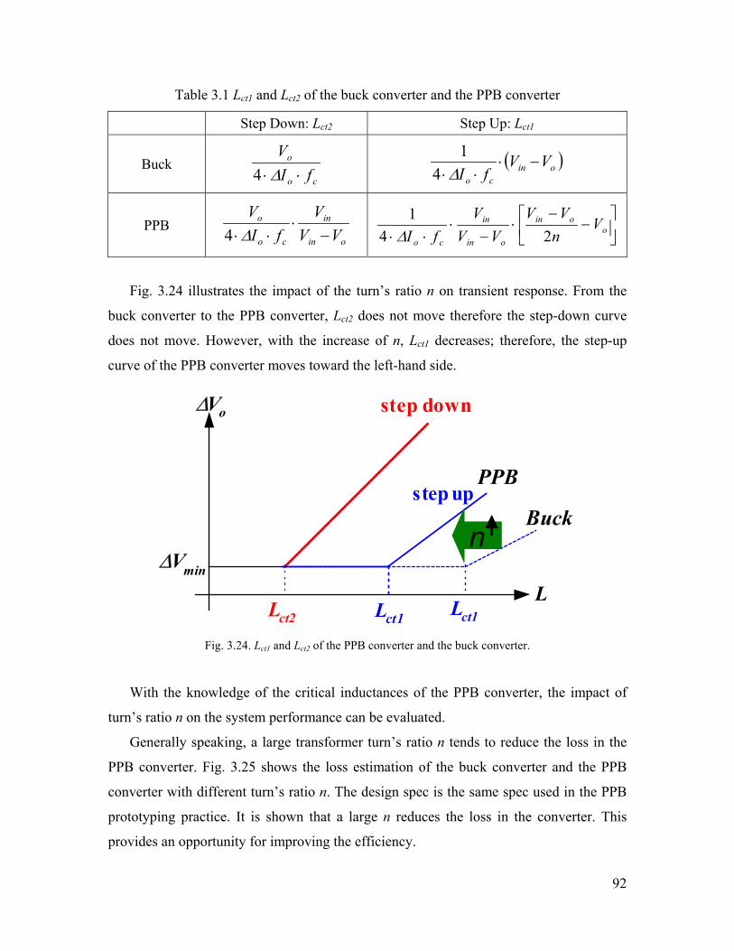
92
Table 3.1 Lct1 and Lct2 of the buck converter and the PPB converter
Step Down: Lct2 Step Up: Lct1
Buck co
o
fIV
⋅⋅ ∆4 ( )oinco
VVfI
−⋅⋅⋅∆4
1
PPB oin
in
co
o
VVV
fIV
−⋅
⋅⋅∆4
−−
⋅−
⋅⋅⋅ o
oin
oin
in
co
VnVV
VVV
fI 241
∆
Fig. 3.24 illustrates the impact of the turn’s ratio n on transient response. From the
buck converter to the PPB converter, Lct2 does not move therefore the step-down curve
does not move. However, with the increase of n, Lct1 decreases; therefore, the step-up
curve of the PPB converter moves toward the left-hand side.
L
∆Vo
∆Vmin
step down
Lct2 Lct1
Buckstep up
Lct1
PPB
nn
Fig. 3.24. Lct1 and Lct2 of the PPB converter and the buck converter.
With the knowledge of the critical inductances of the PPB converter, the impact of
turn’s ratio n on the system performance can be evaluated.
Generally speaking, a large transformer turn’s ratio n tends to reduce the loss in the
PPB converter. Fig. 3.25 shows the loss estimation of the buck converter and the PPB
converter with different turn’s ratio n. The design spec is the same spec used in the PPB
prototyping practice. It is shown that a large n reduces the loss in the converter. This
provides an opportunity for improving the efficiency.

93
Tota
l Los
s(W
)
0
2
4
6
8
10
12
PPBn=1
PPBn=2
PPBn=3buck
Fig. 3.25. Loss estimation of the buck converter and the PPB converter with different turn’s ratio n.
As discussed in Chapter 2, the critical inductance should be the smaller of Lct1 and
Lct2. In a 12V-input buck VR, the relationship between Lct1 and Lct2 is very clear:
Lct2<<Lct1, so the critical inductance Lct is Lct2. However, in a PPB converter, this
relationship is not that certain. Since large n moves the step-up curve toward the left-hand
side while the step-down curve is intact, Lct2 does not change but Lct1 decreases as n
increases. Depending on the relationship of Lct1 and Lct2, there are three possible
scenarios. Fig. 3.26 (a) shows the first scenario: Lct1>Lct2, when the step-up curve stays at
the right-hand side of the step-down curve. Lct should be Lct2 in this case; Fig. 3.26 (b)
shows the second scenario: Lct1=Lct2, when the step-up curve and the step-down curve
overlap. Lct is either Lct2 or Lct1 in this case; Fig. 3.26 (c) shows the third scenario:
Lct1<Lct2, when the step-up curve moves to the left-hand side of the step-down curve. Lct
should be Lct1 in this case.
The above three scenarios have different transient responses. The dark circle in Fig.
3.26 indicates the real inductance used. It is kept the same in the three cases. In Fig. 3.26
(a) and (b), the real inductance is equal to Lct; in Fig. 3.26 (c) the real inductance is larger
than Lct, therefore step up creates a larger voltage spike than step down does. The
transient response is worse.
So although a large n improves efficiency, one should use caution when increasing n.
When n is increased, as long as n satisfies Lct2≤Lct1, the larger n the higher the efficiency,
and the transient response is the same. If n is too large such that Lct2>Lct1, with the
increase of n, efficiency is improved but transient response is worsened. The n value that
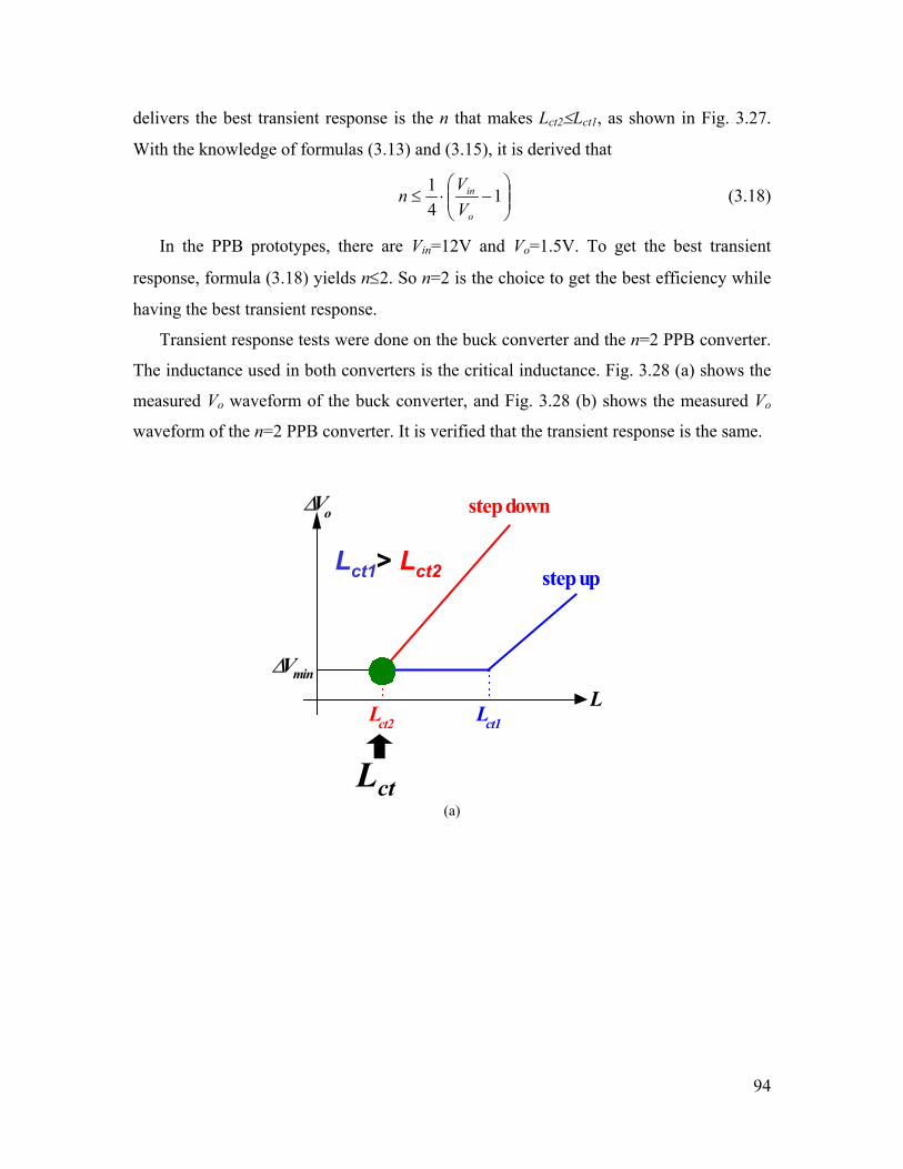
94
delivers the best transient response is the n that makes Lct2≤Lct1, as shown in Fig. 3.27.
With the knowledge of formulas (3.13) and (3.15), it is derived that
−⋅≤ 1
41
o
in
VV
n (3.18)
In the PPB prototypes, there are Vin=12V and Vo=1.5V. To get the best transient
response, formula (3.18) yields n≤2. So n=2 is the choice to get the best efficiency while
having the best transient response.
Transient response tests were done on the buck converter and the n=2 PPB converter.
The inductance used in both converters is the critical inductance. Fig. 3.28 (a) shows the
measured Vo waveform of the buck converter, and Fig. 3.28 (b) shows the measured Vo
waveform of the n=2 PPB converter. It is verified that the transient response is the same.
L
∆Vo
∆Vmin
step down
Lct2
step up
Lct1
Lct1> Lct2
Lct (a)
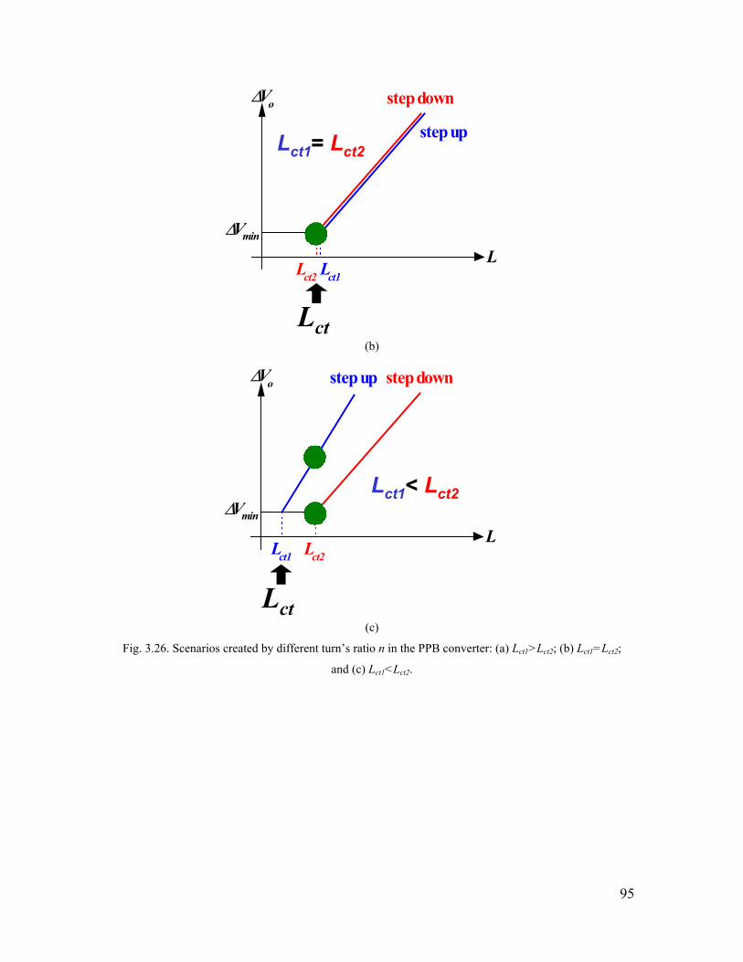
95
L
∆Vo
∆Vmin
step down
Lct2
step up
Lct1
Lct1= Lct2
Lct (b)
L
∆Vo
∆Vmin
step down
Lct2
step up
Lct1
Lct1< Lct2
Lct (c)
Fig. 3.26. Scenarios created by different turn’s ratio n in the PPB converter: (a) Lct1>Lct2; (b) Lct1=Lct2;
and (c) Lct1<Lct2.
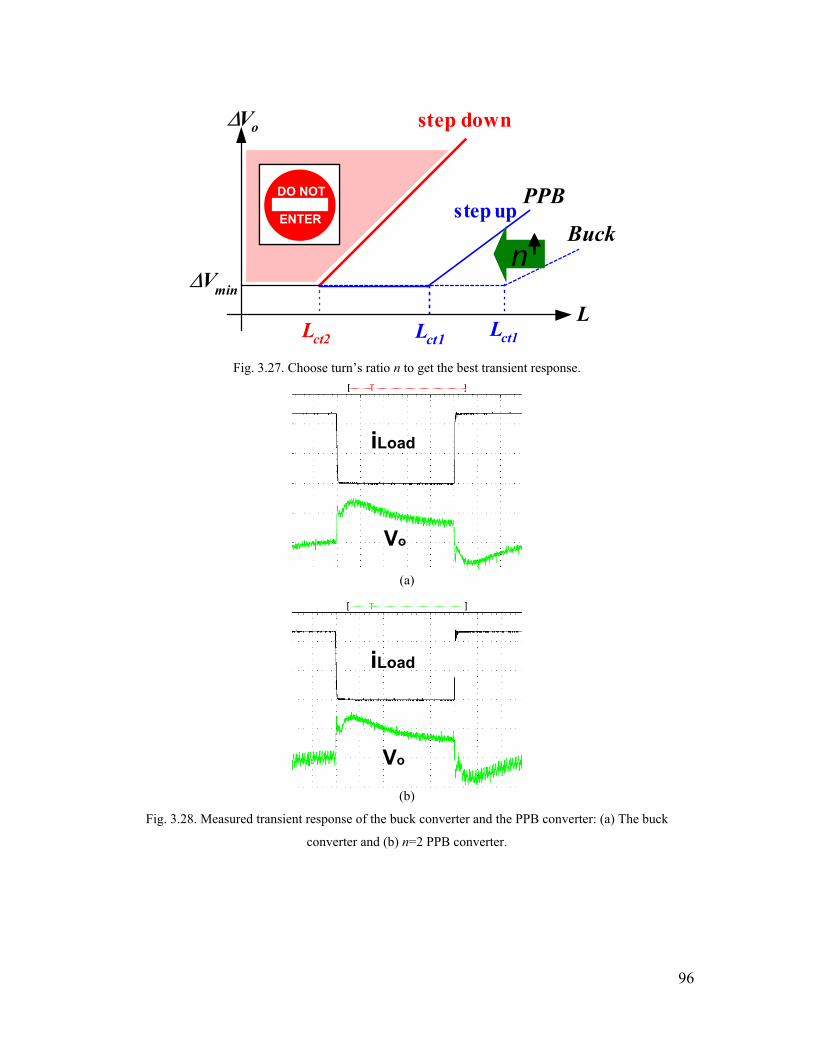
96
L
∆Vo
∆Vmin
step down
Lct2 Lct1
Buckstep up
Lct1
PPB
nn
DO NOT
ENTER
DO NOT
ENTER
Fig. 3.27. Choose turn’s ratio n to get the best transient response.
iLoad
Vo
(a)
iLoad
Vo
(b)
Fig. 3.28. Measured transient response of the buck converter and the PPB converter: (a) The buck
converter and (b) n=2 PPB converter.
97
Since today’s 12V-input buck VRs use an inductance larger than the critical
inductance, VR transient response is worse than what it otherwise would be if critical
inductance were used. Considering the PPB converter uses the critical inductance, the
PPB converter has better transient response than today’s VR approach.
3.5. Summary.
High switching frequency reduces the output capacitors needed, which is beneficial in
terms of size and cost. However, the multiphase buck VR suffers low efficiency at high
switching frequency. Since the extreme duty cycle is the fundamental limitation,
extending the duty cycle is the solution discussed in this chapter.
Employing the transformer concept can extend duty cycle, and therefore offer an
opportunity to improve efficiency. The tapped-inductor buck converter extends the duty
cycle, thereby improving efficiency. However, the tapped-inductor buck converter suffers
a detrimental voltage spike caused by the leakage inductor. Other solutions are needed.
Solutions in isolated converters can be applied to the non-isolated VR application
with some modification. The push-pull buck (PPB) converter is proposed as a solution.
The voltage spike is clamped and the efficiency is improved compared with the buck
converter. Integrated magnetic techniques can be used to further improve the efficiency
and simplify the implementation.
The transformer turn’s ratio n plays an important role impacting the transient
response. Lct2 is not affected while Lct1 is decreased with the increase of n. The critical
inductance is the smaller one of Lct1 and Lct2. When n is increasing, as long as n satisfies
Lct2≤Lct1, the larger n delivers high efficiency and the transient response is the same. If n
is too large, such that Lct2>Lct1, with the increase of n efficiency is improved but transient
response is worsened.
The experimental test results prove that the PPB converter can improve efficiency
while achieving good transient response.
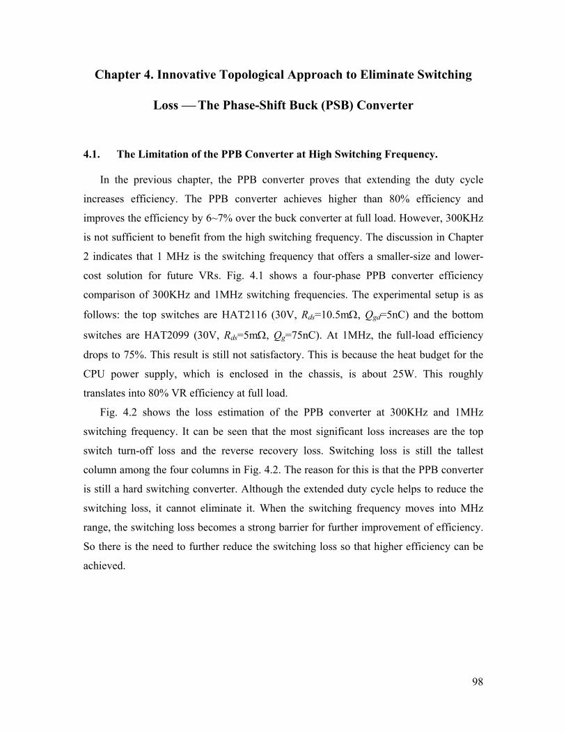
98
Chapter 4. Innovative Topological Approach to Eliminate Switching
Loss The Phase-Shift Buck (PSB) Converter
4.1. The Limitation of the PPB Converter at High Switching Frequency.
In the previous chapter, the PPB converter proves that extending the duty cycle
increases efficiency. The PPB converter achieves higher than 80% efficiency and
improves the efficiency by 6~7% over the buck converter at full load. However, 300KHz
is not sufficient to benefit from the high switching frequency. The discussion in Chapter
2 indicates that 1 MHz is the switching frequency that offers a smaller-size and lower-
cost solution for future VRs. Fig. 4.1 shows a four-phase PPB converter efficiency
comparison of 300KHz and 1MHz switching frequencies. The experimental setup is as
follows: the top switches are HAT2116 (30V, Rds=10.5mΩ, Qgd=5nC) and the bottom
switches are HAT2099 (30V, Rds=5mΩ, Qg=75nC). At 1MHz, the full-load efficiency
drops to 75%. This result is still not satisfactory. This is because the heat budget for the
CPU power supply, which is enclosed in the chassis, is about 25W. This roughly
translates into 80% VR efficiency at full load.
Fig. 4.2 shows the loss estimation of the PPB converter at 300KHz and 1MHz
switching frequency. It can be seen that the most significant loss increases are the top
switch turn-off loss and the reverse recovery loss. Switching loss is still the tallest
column among the four columns in Fig. 4.2. The reason for this is that the PPB converter
is still a hard switching converter. Although the extended duty cycle helps to reduce the
switching loss, it cannot eliminate it. When the switching frequency moves into MHz
range, the switching loss becomes a strong barrier for further improvement of efficiency.
So there is the need to further reduce the switching loss so that higher efficiency can be
achieved.

99
Output Current (A)10 20 30 40 50 60 70 800
Effic
ienc
y
60%65%70%75%80%85%90%95%
100%
1MHz PPB
300KHz PPB
Fig. 4.1. Efficiency comparison of the PPB converter switching at 300 KHz and 1 MHz.
0
2
4
6
8
10
12
14
TopConduction
Top SwitchTurn-off
ReverseRecovery
BottomConduction
Los
s (W
)
300KHz PPB1MHz PPB
Fig. 4.2. Loss analysis of the PPB converter switching at 300 KHz and 1 MHz.
4.2. The Proposed Soft-Switched Phase-Shift Buck (PSB) Converter.
To further reduce the switching loss, soft switching is needed. There have been
tremendous efforts made on soft-switching schemes for topologies with transformer
isolation. The phase-shift controlled full-bridge converter is a well-known and widely
used one. Fig. 4.3 shows a full-bridge converter with current-doubler output. The primary
switches Q1~Q4 are phase-shift controlled, and Q5~Q6 are synchronous FETs. This
topology has soft-switching capability, and therefore has great potential for high-
frequency applications.
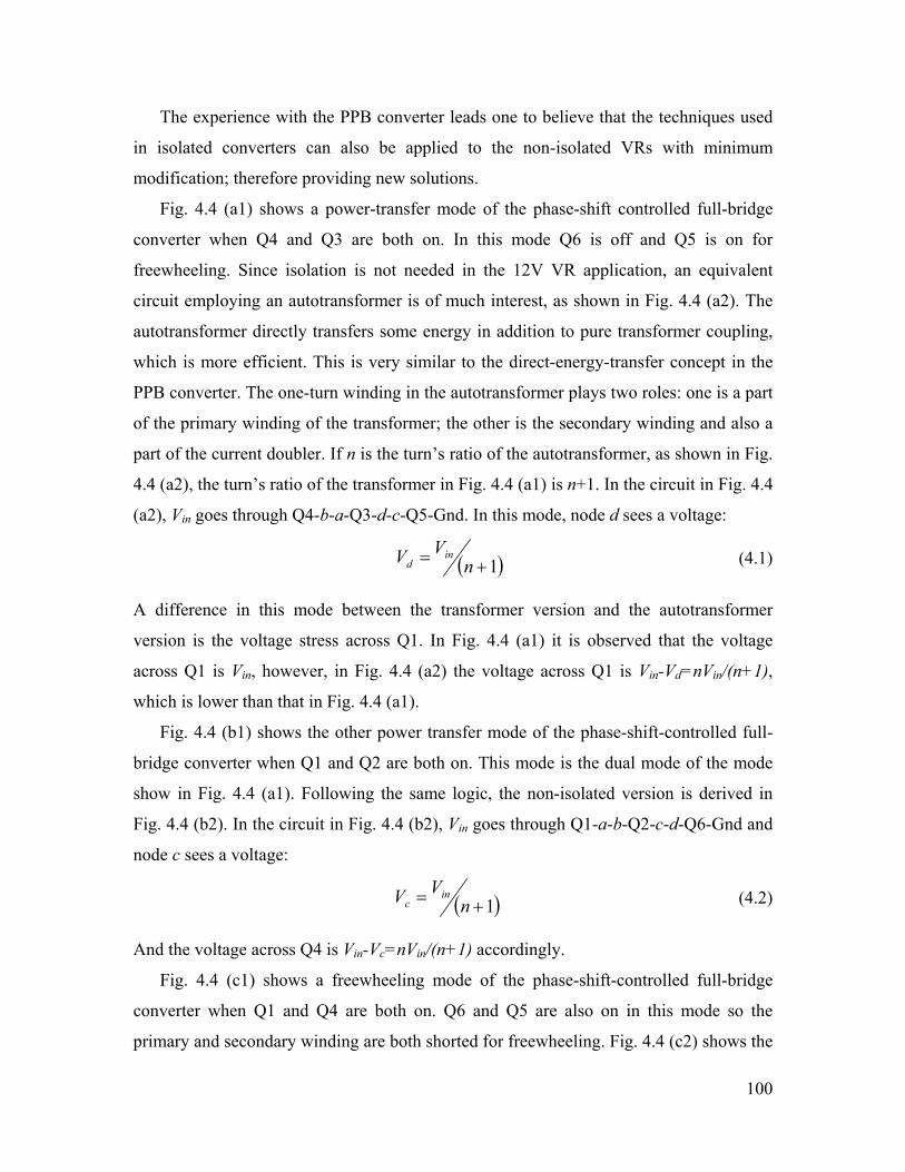
100
The experience with the PPB converter leads one to believe that the techniques used
in isolated converters can also be applied to the non-isolated VRs with minimum
modification; therefore providing new solutions.
Fig. 4.4 (a1) shows a power-transfer mode of the phase-shift controlled full-bridge
converter when Q4 and Q3 are both on. In this mode Q6 is off and Q5 is on for
freewheeling. Since isolation is not needed in the 12V VR application, an equivalent
circuit employing an autotransformer is of much interest, as shown in Fig. 4.4 (a2). The
autotransformer directly transfers some energy in addition to pure transformer coupling,
which is more efficient. This is very similar to the direct-energy-transfer concept in the
PPB converter. The one-turn winding in the autotransformer plays two roles: one is a part
of the primary winding of the transformer; the other is the secondary winding and also a
part of the current doubler. If n is the turn’s ratio of the autotransformer, as shown in Fig.
4.4 (a2), the turn’s ratio of the transformer in Fig. 4.4 (a1) is n+1. In the circuit in Fig. 4.4
(a2), Vin goes through Q4-b-a-Q3-d-c-Q5-Gnd. In this mode, node d sees a voltage:
( )1+= nVV in
d (4.1)
A difference in this mode between the transformer version and the autotransformer
version is the voltage stress across Q1. In Fig. 4.4 (a1) it is observed that the voltage
across Q1 is Vin, however, in Fig. 4.4 (a2) the voltage across Q1 is Vin-Vd=nVin/(n+1),
which is lower than that in Fig. 4.4 (a1).
Fig. 4.4 (b1) shows the other power transfer mode of the phase-shift-controlled full-
bridge converter when Q1 and Q2 are both on. This mode is the dual mode of the mode
show in Fig. 4.4 (a1). Following the same logic, the non-isolated version is derived in
Fig. 4.4 (b2). In the circuit in Fig. 4.4 (b2), Vin goes through Q1-a-b-Q2-c-d-Q6-Gnd and
node c sees a voltage:
( )1+= nVV in
c (4.2)
And the voltage across Q4 is Vin-Vc=nVin/(n+1) accordingly.
Fig. 4.4 (c1) shows a freewheeling mode of the phase-shift-controlled full-bridge
converter when Q1 and Q4 are both on. Q6 and Q5 are also on in this mode so the
primary and secondary winding are both shorted for freewheeling. Fig. 4.4 (c2) shows the

101
corresponding autotransformer version. When Q1, Q4, Q6 and Q5 are on, the
autotransformer windings are also shorted for freewheeling.
Fig. 4.4 (d1) shows the other freewheeling mode of the phase-shift-controlled full-
bridge converter when Q2, Q3, Q5 and Q6 are all on. Fig. 4.4 (d2) shows the
corresponding autotransformer version.
Co RL
VoL
L
1 *
Vin
n* +1
b c
a d
e
Q5Q4
Q1
Q2
Q3 Q6
Fig. 4.3. The full-bridge converter with current-doubler output.
Co RL
VoL
L
1 *
Vin
n*
Q1 Q3
Q4 Q2
Q6
Q5
b c
d
e
a
+1
Co RL
VoL
L
1 *
Vin
n*
Q1 Q3
Q4 Q2
Q6
Q5
a
b c
d
e
(a1) (a2)
Co RL
VoL
L
1 *
Vin
n*
Q1 Q3
Q4 Q2
Q6
Q5
b c
d
e
a
+1
Co RL
VoL
L
1 *
Vin
n*
Q1 Q3
Q4 Q2
Q6
Q5
b c
a d
e
(b1) (b2)
Co RL
VoL
L
1 *
Vin
n*
Q1 Q3
Q4 Q2
Q6
Q5
b c
d
e
a
+1
Co RL
VoL
L
1 *
Vin
n*
Q1 Q3
Q4 Q2
Q6
Q5
a
b c
d
e
(c1) (c2)

102
Co RL
VoL
L
1 *
Vin
n*
Q1 Q3
Q4 Q2
Q6
Q5
b c
d
e
a
+1
Co RL
VoL
L
1 *
Vin
n*
Q1 Q3
Q4 Q2
Q6
Q5
b c
a d
e
(d1) (d2) Fig. 4.4. Deriving an autotransformer version from the full-bridge converter: (a1) the transformer
version, when Q4 and Q3 are “on”, (a2) the autotransformer version, when Q4 and Q3 are “on”, (b1)the
transformer version, when Q1 and Q2 are “on”, (b2) the autotransformer version, when Q1 and Q2 are
“on”, (c1) the transformer version, when Q1 and Q4 are “on”, (c2) the autotransformer version, when Q1
and Q4 are “on”, (d1) the transformer version, when Q2 and Q3 are “on”, and (d2) the autotransformer
version, when Q2 and Q3 are “on”.
The proposed phase-shift buck (PSB) converter in Fig. 4.5 realizes the conceptual
converter featuring the equivalent circuits shown in Fig. 4.4 (a2), (b2), (c2) and (d2).
Q1~Q6 are MOSFETs instead of ideal switches.
As in a full-bridge converter, the PSB converter can be controlled in a traditional
PWM fashion or a phase-shifted fashion. The traditional PWM control leads to hard
switching of the top switches Q1~Q4, while phase-shift control allows soft switching of
Q1~Q4, which is desirable at high switching frequency. Fig. 4.6 shows the operation
principle of the phase-shift control. Vab and ip are the transformer’s primary voltage and
current. They are in exactly the same shapes as those in a phase-shift controlled full
bridge converter. Vc and Vd are nodes “c” and “d” voltages. VDS1 and iDS1 are Q1 drain-
source voltage and current, etc. Duration t7~t8 is the power transfer mode in Fig. 4.4 (a2),
and duration t2~t3 is the power transfer mode in Fig. 4.4 (b2). Duration t9~t0 is the
freewheeling mode in Fig. 4.4 (c2) and duration t4~t5 is the freewheeling mode in Fig. 4.4
(d2).
Shown in Fig. 4.7 are the subintervals of the circuit operation associated with Fig.
4.6. The transformer primary current ip is defined as flowing from node “a” to “b”; Lk is
the transformer leakage inductor; and capacitors C1~C4 are the drain-source capacitors of
switches Q1~Q4.
Fig. 4.7 (a) shows the subinterval t0~t1. Before t0 the circuit is in the freewheeling
mode and the transformer is shorted. The primary current ip is flowing from node “b” to

103
“a”. At t0, Q4 is turned off. However, ip continues flowing due to the existence of Lk,
therefore C2 is discharged and C4 is charged in a fashion determined by the L-C
resonance formed by Lk and the parallel of C2 and C4. Given sufficient energy stored in
Lk, C2 can be fully discharged, after which ip flows through the body diode of Q2.
Fig. 4.7 (b) shows the subinterval t1~t2. At t1, Q2 is turned on. Because ip is flowing
through the body diode of Q2, Q2 is turned on at zero-voltage condition, which
eliminates the turn-on loss. In the meantime, Q5 and Q6 are still carrying current for
freewheeling, which means the transformer is still shorted. Thus the voltage across nodes
“a” and “b” is applied to Lk and builds up ip in the direction from “a” to ”b”. As a result,
the current through Q5 decreases until at t2 it reaches zero.
Fig. 4.7 (c) shows the subinterval t2~t3. This is a power transfer mode. The
transformer acts as an autotransformer and L1 is being charged while L2 is being
discharged. The transformer primary current ip is flowing from node “a” to “b”.
Fig. 4.7 (d) shows the subinterval t3~t4. At t3, Q1 is turned off, but the transformer
primary current ip continues flowing from node “a” to “b”. Because ip is the reflected
output inductor current, C3 is discharged and C1 is charged linearly until at t4 when C3 is
fully discharged so ip flows through the body diode of Q3.
Fig. 4.7 (e) shows the subinterval t4~t5. This is a freewheeling mode. Switches Q2,
Q3, Q5 and Q6 are on so the transformer is shorted.
Fig. 4.7 (f) shows the subinterval t5~t6. This is the dual mode of the subinterval t0~t1.
At t5, ip is flowing from node “a” to “p”. At t5, Q2 is turned off. However, ip continues
flowing due to the existence of Lk, therefore C4 is discharged and C2 is charged in a
fashion determined by the L-C resonance formed by Lk and the parallel of C2 and C4.
Given sufficient energy stored in Lk, C4 can be fully discharged, after which ip flows
through the body diode of Q4.
Fig. 4.7 (g) shows the subinterval t6~t7. This is the dual mode of the subinterval t1~t2.
At t6, Q4 is turned on. Because ip is flowing through the body diode of Q4, Q4 is turned
on at zero-voltage condition, which eliminates the turn-on loss. In the meantime, the
transformer is still shorted. The voltage across nodes “b” and “a” builds up ip in the
direction from “b” to ”a”. As a result, the current through Q6 decreases until at t7 it
reaches zero.
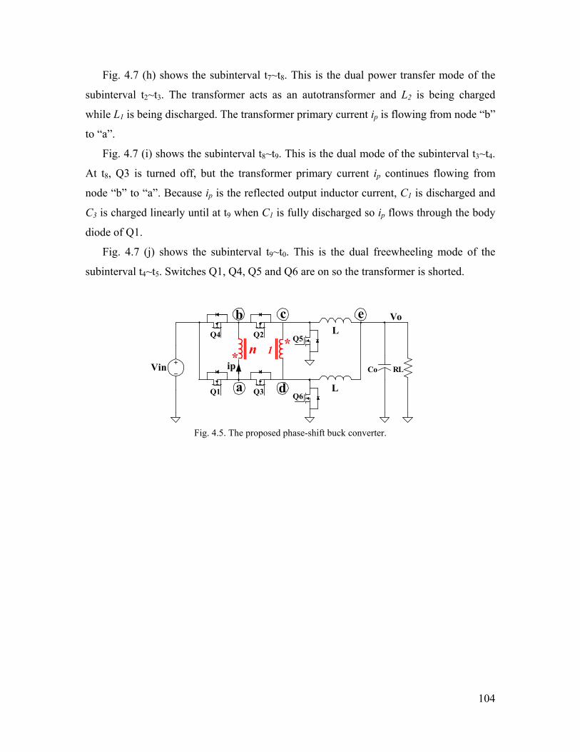
104
Fig. 4.7 (h) shows the subinterval t7~t8. This is the dual power transfer mode of the
subinterval t2~t3. The transformer acts as an autotransformer and L2 is being charged
while L1 is being discharged. The transformer primary current ip is flowing from node “b”
to “a”.
Fig. 4.7 (i) shows the subinterval t8~t9. This is the dual mode of the subinterval t3~t4.
At t8, Q3 is turned off, but the transformer primary current ip continues flowing from
node “b” to “a”. Because ip is the reflected output inductor current, C1 is discharged and
C3 is charged linearly until at t9 when C1 is fully discharged so ip flows through the body
diode of Q1.
Fig. 4.7 (j) shows the subinterval t9~t0. This is the dual freewheeling mode of the
subinterval t4~t5. Switches Q1, Q4, Q5 and Q6 are on so the transformer is shorted.
Co RL
VoL
L
1 *
Vin
n*
b c
a d
e
Q5Q4
Q1
Q2
Q3 Q6
ip
Fig. 4.5. The proposed phase-shift buck converter.

105
Q1 Q3Q4 Q2 Q4
Vab iP
vc
vd
vDS1
vDS3
vDS4
vDS2
iDS1
iDS3
iDS4
iDS2
Q5Q5Q6 Q6Q5
Q6
Q3 Q1
Q6
t0t1
t3 t5 t7 t8t9
Vin(n+1)
nVinn+1
Vin
Vin
Vin
Vin
nVinn+1
t4 t9t2t6
Fig. 4.6. The operation principle of the proposed phase-shift buck converter.
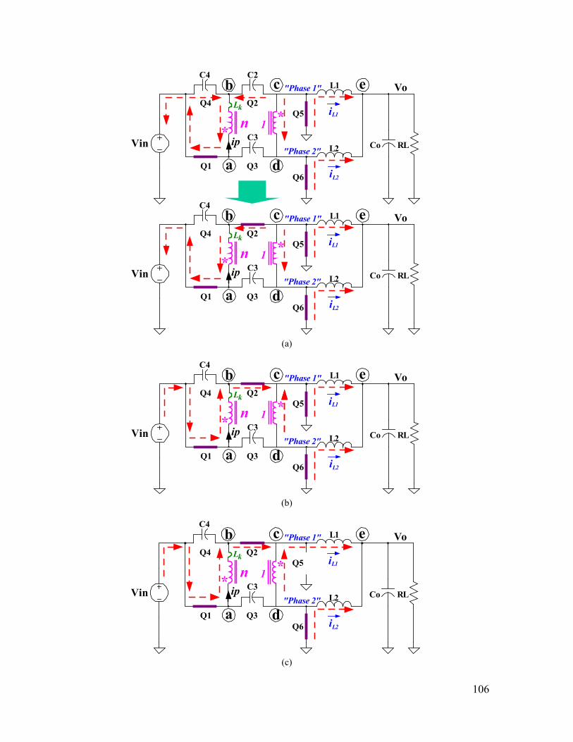
106
Co RL
VoL1
L2
1 *
Vin
n*
Q1 Q3
Q4 Q2
Q6
Q5
a
b c
d
e"Phase 1"
"Phase 2"
kL iL1
iL2
ip
C4 C2
C3
Co RL
VoL1
L2
1 *
Vin
n*
Q1 Q3
Q4 Q2
Q6
Q5
a
b c
d
e"Phase 1"
"Phase 2"
kL iL1
iL2
ip
C4
C3
(a)
Co RL
VoL1
L2
1 *
Vin
n*
Q1 Q3
Q4 Q2
Q6
Q5
a
b c
d
e"Phase 1"
"Phase 2"
kL iL1
iL2
ip
C4
C3
(b)
Co RL
VoL1
L2
1 *
Vin
n*
Q1 Q3
Q4 Q2
Q6
Q5
a
b c
d
e"Phase 1"
"Phase 2"
kL iL1
iL2
ip
C4
C3
(c)
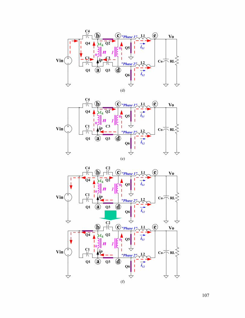
107
Co RL
VoL1
L2
1 *
Vin
n*
Q1 Q3
Q4 Q2
Q6
Q5
a
b c
d
e"Phase 1"
"Phase 2"
kL iL1
iL2
ip
C4
C3C1
(d)
Co RL
VoL1
L2
1 *
Vin
n*
Q1 Q3
Q4 Q2
Q6
Q5
a
b c
d
e"Phase 1"
"Phase 2"
kL iL1
iL2
ip
C4
C3C1
(e)
Co RL
VoL1
L2
1 *
Vin
n*
Q1 Q3
Q4 Q2
Q6
Q5
a
b c
d
e"Phase 1"
"Phase 2"
kL iL1
iL2
ip
C4 C2
C1
Co RL
VoL1
L2
1 *
Vin
n*
Q1 Q3
Q4 Q2
Q6
Q5
a
b c
d
e"Phase 1"
"Phase 2"
kL iL1
iL2
ip
C2
C1
(f)
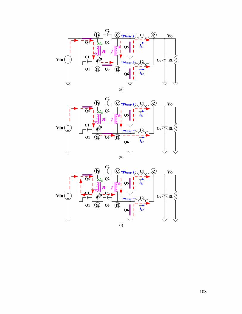
108
Co RL
VoL1
L2
1 *
Vin
n*
Q1 Q3
Q4 Q2
Q6
Q5
a
b c
d
e"Phase 1"
"Phase 2"
kL iL1
iL2
ip
C2
C1
(g)
Co RL
VoL1
L2
1 *
Vin
n*
Q1 Q3
Q4 Q2
Q6
Q5
a
b c
d
e"Phase 1"
"Phase 2"
kL iL1
iL2
ip
C2
C1
(h)
Co RL
VoL1
L2
1 *
Vin
n*
Q1 Q3
Q4 Q2
Q6
Q5
a
b c
d
e"Phase 1"
"Phase 2"
kL iL1
iL2
ip
C2
C1 C3
(i)

109
Co RL
VoL1
L2
1 *
Vin
n*
Q1 Q3
Q4 Q2
Q6
Q5
a
b c
d
e"Phase 1"
"Phase 2"
kL iL1
iL2
ip
C2
C3
(j)
Fig. 4.7. Subintervals of the Circuit Operation: (a) t0~t1, (b) t1~t2, (c) t2~t3, (d) t3~t4, (e) t4~t5, (f) t5~t6, (g)
t6~t7, (h) t7~t8, (i) t8~t9, (j) t9~t0.
In Fig. 4.7, the voltage potentials of nodes “c” and “d” during the power transfer
modes are already expressed in formulas (4.1) and (4.2); during the freewheeling modes
these voltages are zero. These voltages are applied to the output L-C filter. Since the
voltage waveforms of nodes “c” and “d” are the same, with only 180-phase shift, the PSB
converter behaves just like a two-phase interleaved buck converter. The input voltage of
the equivalent buck converter is Vin/(n+1). Accordingly, nodes “c” and “d” are marked as
“Phase 1” and “Phase 2”.
For convenience in comparison with the buck converter, the duty cycle D is defined
as the ratio of the duration of a power transfer mode and a full switching cycle. Then the
voltage conversion gain of the PSB converter is
( )1+= nDVV in
o (4.3)
A design example: Vin=12V, Vo=1.5V, n=1, will yield D=0.25.
The above analysis shows that the PSB converter is capable of realizing the ZVS turn
on of the top switches Q1~Q4. This fact makes it possible to reduce the switching loss by
paralleling snubber capacitors with Q1~Q4. A large drain-source capacitor slows down
the drain-source voltage rise during the turn off of the switch, which reduces the turn-off
loss. The energy stored in the capacitor is recovered during the ZVS turn on; therefore the
switching loss is minimized.
The “phase” voltages are expressed by formulas (4.1) and (4.2). With the transformer
turn’s ratio equal to n, the phase voltages are reduced when compared with that of the
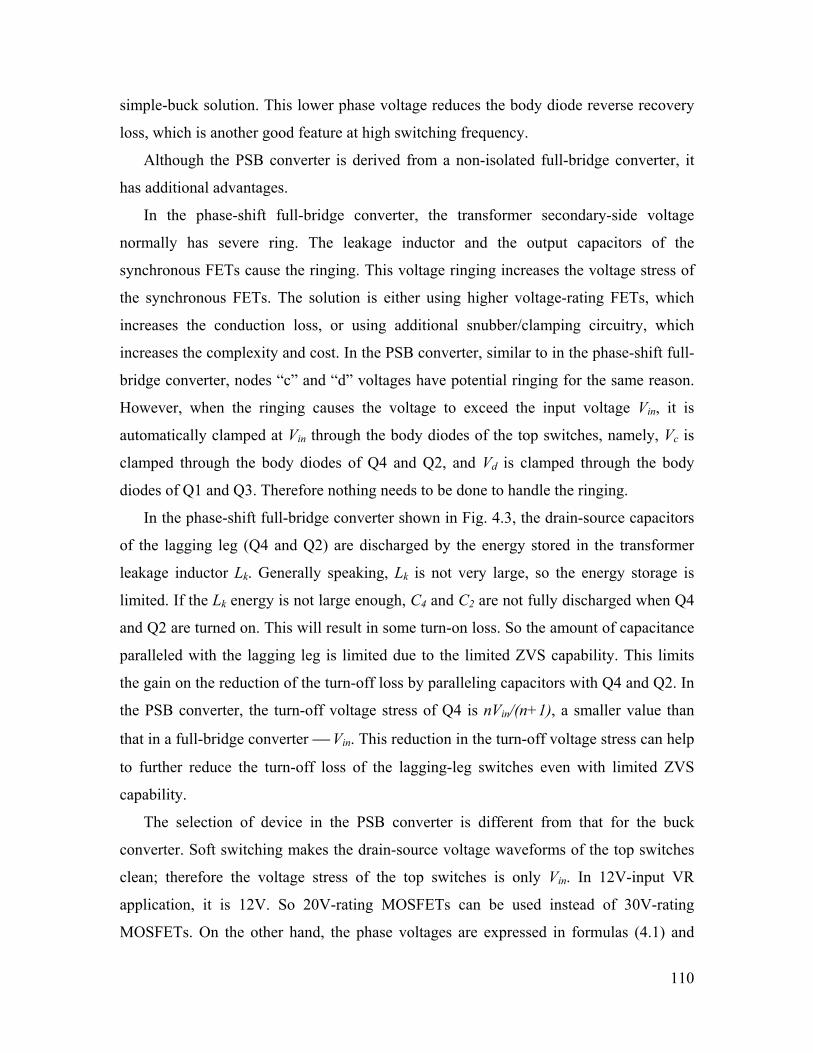
110
simple-buck solution. This lower phase voltage reduces the body diode reverse recovery
loss, which is another good feature at high switching frequency.
Although the PSB converter is derived from a non-isolated full-bridge converter, it
has additional advantages.
In the phase-shift full-bridge converter, the transformer secondary-side voltage
normally has severe ring. The leakage inductor and the output capacitors of the
synchronous FETs cause the ringing. This voltage ringing increases the voltage stress of
the synchronous FETs. The solution is either using higher voltage-rating FETs, which
increases the conduction loss, or using additional snubber/clamping circuitry, which
increases the complexity and cost. In the PSB converter, similar to in the phase-shift full-
bridge converter, nodes “c” and “d” voltages have potential ringing for the same reason.
However, when the ringing causes the voltage to exceed the input voltage Vin, it is
automatically clamped at Vin through the body diodes of the top switches, namely, Vc is
clamped through the body diodes of Q4 and Q2, and Vd is clamped through the body
diodes of Q1 and Q3. Therefore nothing needs to be done to handle the ringing.
In the phase-shift full-bridge converter shown in Fig. 4.3, the drain-source capacitors
of the lagging leg (Q4 and Q2) are discharged by the energy stored in the transformer
leakage inductor Lk. Generally speaking, Lk is not very large, so the energy storage is
limited. If the Lk energy is not large enough, C4 and C2 are not fully discharged when Q4
and Q2 are turned on. This will result in some turn-on loss. So the amount of capacitance
paralleled with the lagging leg is limited due to the limited ZVS capability. This limits
the gain on the reduction of the turn-off loss by paralleling capacitors with Q4 and Q2. In
the PSB converter, the turn-off voltage stress of Q4 is nVin/(n+1), a smaller value than
that in a full-bridge converter Vin. This reduction in the turn-off voltage stress can help
to further reduce the turn-off loss of the lagging-leg switches even with limited ZVS
capability.
The selection of device in the PSB converter is different from that for the buck
converter. Soft switching makes the drain-source voltage waveforms of the top switches
clean; therefore the voltage stress of the top switches is only Vin. In 12V-input VR
application, it is 12V. So 20V-rating MOSFETs can be used instead of 30V-rating
MOSFETs. On the other hand, the phase voltages are expressed in formulas (4.1) and
111
(4.2). They are reduced compared with that in the buck converter. In a 12V-input buck
VR, the switching node (“phase”) voltage suffers high-voltage ringing. The ringing is so
high that 30V-rating MOSFETs are needed. The lower “phase” voltage in the phase-shift
buck converter can alleviate the “phase” voltage ringing; therefore 20V MOSFETs can be
used. Since 20V MOSFETs have better performance than 30V MOEFETS, the phase-
shift buck converter can benefit from the lower voltage rating MOSFETs.
Fig. 4.8 shows the loss estimation of three converters: the buck converter, the PPB
converter, and the PSB converter. In the buck converter and the PPB converter, 30V
MOSFETs are needed. So the top switches are HAT2116 (30V, Rds=10.5mΩ, Qgd=5nC),
and the bottom switches are HAT2099 (30V, Rds=5mΩ, Qg=75nC). In the PSB converter,
all switches are Si4864 (20V, Rds=3.5mΩ, Qg=47nC). All the three converters use four-
phase structure to carry 70A output current. The input voltage is 12V, the output voltage
is 1.3V, the inductance is 150nH, and the switching frequency is 1MHz.
From Fig. 4.8, it is seen that the PSB converter greatly reduces the switching loss.
Also because of the lower “phase” voltage, the body-diode reverse recovery loss is
reduced compared to the buck converter. As far as top-switch conduction losses are
concerned, the rms currents of the top switches are the largest for the PSB converters due
to the current freewheeling. However, because the PSB converter can use 20V
MOSFETs, which have lower Rds(on), the final results of the total top-switch conduction
loss is even smaller than in the other two converters. The same thing happens to the
bottom-switch conduction loss. Although the rms current is the largest, the PSB converter
does not suffer much from the bottom-switch conduction loss.
Getting simple drivers for the top switches is important. The most convenient method
today is to use a bootstrap driver. Fig. 4.9 (a) shows a conventional bootstrap driver used
to drive a top-bottom switch combination. Q1 is the top switch and Q2 is the bottom
switch. The switching node “SW” is connected to the bootstrap driver; it is also
connected to one terminal of a bootstrap capacitor. When Q2 is on, “SW” is pulled down
to ground, thus a bootstrap capacitor is charged by the bias voltage supplier of the driver.
Then the capacitor provides energy to charge the gate capacitor of Q1 during the turn on
of Q1. The device arrangement in the PSB converter is different from Fig. 4.9 (a). Fig.
4.9 (b) shows one leg of the PSB converter. There are three devices in series; therefore
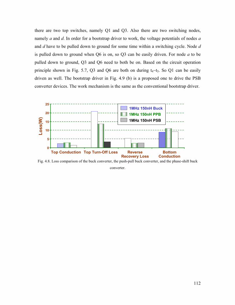
112
there are two top switches, namely Q1 and Q3. Also there are two switching nodes,
namely a and d. In order for a bootstrap driver to work, the voltage potentials of nodes a
and d have to be pulled down to ground for some time within a switching cycle. Node d
is pulled down to ground when Q6 is on, so Q3 can be easily driven. For node a to be
pulled down to ground, Q3 and Q6 need to both be on. Based on the circuit operation
principle shown in Fig. 5.7, Q3 and Q6 are both on during t4~t5. So Q1 can be easily
driven as well. The bootstrap driver in Fig. 4.9 (b) is a proposed one to drive the PSB
converter devices. The work mechanism is the same as the conventional bootstrap driver.
0
5
10
15
20
25
Top Conduction Top Turn-Off Loss ReverseRecovery Loss
BottomConduction
Loss
(W)
1MHz 150nH Buck1MHz 150nH PPB1MHz 150nH PSB
Fig. 4.8. Loss comparison of the buck converter, the push-pull buck converter, and the phase-shift buck
converter.
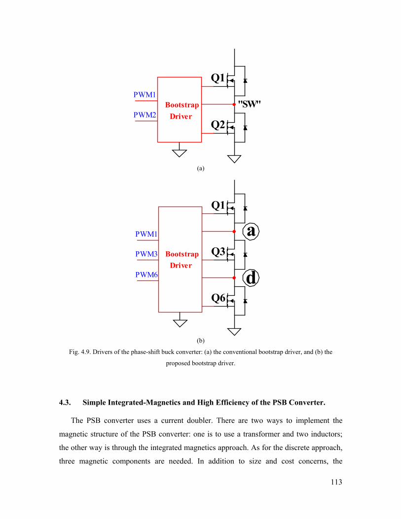
113
Q2
Q1
BootstrapDriver
"SW"PWM1
PWM2
(a)
Q6
Q3
Q1
BootstrapDriver
PWM1
PWM3
PWM6
a
d
(b)
Fig. 4.9. Drivers of the phase-shift buck converter: (a) the conventional bootstrap driver, and (b) the
proposed bootstrap driver.
4.3. Simple Integrated-Magnetics and High Efficiency of the PSB Converter.
The PSB converter uses a current doubler. There are two ways to implement the
magnetic structure of the PSB converter: one is to use a transformer and two inductors;
the other way is through the integrated magnetics approach. As for the discrete approach,
three magnetic components are needed. In addition to size and cost concerns, the
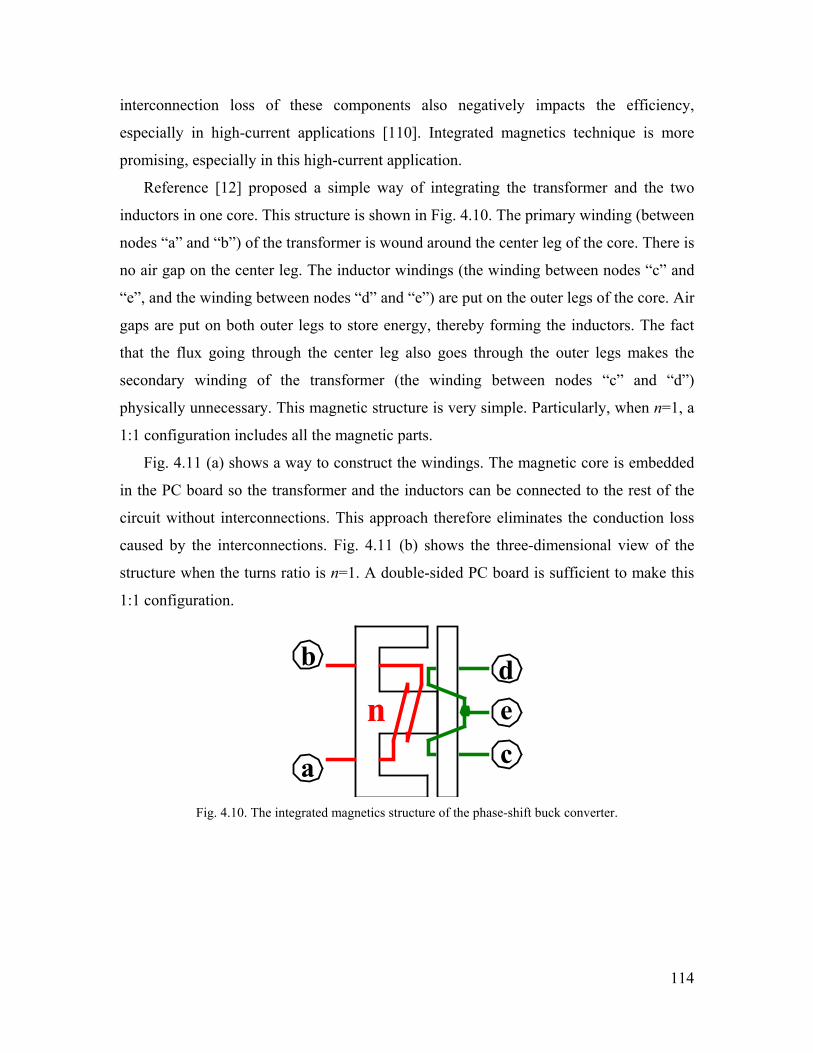
114
interconnection loss of these components also negatively impacts the efficiency,
especially in high-current applications [110]. Integrated magnetics technique is more
promising, especially in this high-current application.
Reference [12] proposed a simple way of integrating the transformer and the two
inductors in one core. This structure is shown in Fig. 4.10. The primary winding (between
nodes “a” and “b”) of the transformer is wound around the center leg of the core. There is
no air gap on the center leg. The inductor windings (the winding between nodes “c” and
“e”, and the winding between nodes “d” and “e”) are put on the outer legs of the core. Air
gaps are put on both outer legs to store energy, thereby forming the inductors. The fact
that the flux going through the center leg also goes through the outer legs makes the
secondary winding of the transformer (the winding between nodes “c” and “d”)
physically unnecessary. This magnetic structure is very simple. Particularly, when n=1, a
1:1 configuration includes all the magnetic parts.
Fig. 4.11 (a) shows a way to construct the windings. The magnetic core is embedded
in the PC board so the transformer and the inductors can be connected to the rest of the
circuit without interconnections. This approach therefore eliminates the conduction loss
caused by the interconnections. Fig. 4.11 (b) shows the three-dimensional view of the
structure when the turns ratio is n=1. A double-sided PC board is sufficient to make this
1:1 configuration.
b deca
n
Fig. 4.10. The integrated magnetics structure of the phase-shift buck converter.
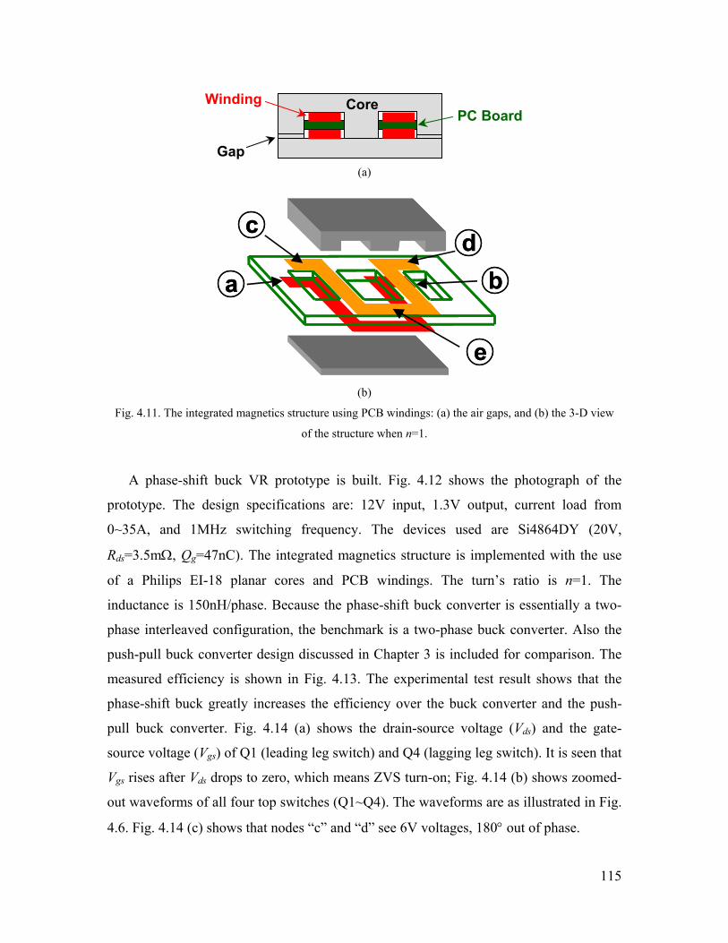
115
PC Board
Gap
Winding Core
(a)
ddbb
cc
aa
ee
(b)
Fig. 4.11. The integrated magnetics structure using PCB windings: (a) the air gaps, and (b) the 3-D view
of the structure when n=1.
A phase-shift buck VR prototype is built. Fig. 4.12 shows the photograph of the
prototype. The design specifications are: 12V input, 1.3V output, current load from
0~35A, and 1MHz switching frequency. The devices used are Si4864DY (20V,
Rds=3.5mΩ, Qg=47nC). The integrated magnetics structure is implemented with the use
of a Philips EI-18 planar cores and PCB windings. The turn’s ratio is n=1. The
inductance is 150nH/phase. Because the phase-shift buck converter is essentially a two-
phase interleaved configuration, the benchmark is a two-phase buck converter. Also the
push-pull buck converter design discussed in Chapter 3 is included for comparison. The
measured efficiency is shown in Fig. 4.13. The experimental test result shows that the
phase-shift buck greatly increases the efficiency over the buck converter and the push-
pull buck converter. Fig. 4.14 (a) shows the drain-source voltage (Vds) and the gate-
source voltage (Vgs) of Q1 (leading leg switch) and Q4 (lagging leg switch). It is seen that
Vgs rises after Vds drops to zero, which means ZVS turn-on; Fig. 4.14 (b) shows zoomed-
out waveforms of all four top switches (Q1~Q4). The waveforms are as illustrated in Fig.
4.6. Fig. 4.14 (c) shows that nodes “c” and “d” see 6V voltages, 180° out of phase.

116
Fig. 4.12. The photograph of the phase-shift buck converter prototype.
2φ Buck
Output Current (A)5 10 15 20 25 30 35 400
Output Current (A)5 10 15 20 25 30 35 400
Effic
ienc
y
60%
65%
70%
75%
80%
85%
90%
Effic
ienc
y
60%
65%
70%
75%
80%
85%
90% PSBPSB
Vo=1.3V, fs=1MHz, L=150nH
PPB
Fig. 4.13. The measured efficiency comparison.

117
Vgs1Vds1
ZVS Turn-on
Vgs4Vds4
ZVS Turn-on
(a)
Vgs4
Vds4
Vgs1
Vds1
Vgs2 Vds2
Vgs3Vds3
(b)
Vc 6V
6VVd
(c)
Fig. 4.14. Test waveforms of the PSB prototype, (a) ZVS turn-on, (b) Top switch waveforms and (c)
Bottom switch waveforms.

118
4.4. The Proposed Matrix-Transformer Phase-shift Buck (MTPSB) Converter.
The PSB converter greatly increases efficiency. However the PSB, which is
essentially a two-phase configuration, uses more devices than a two-phase buck
converter. The large amount of current demanded by the CPU requires VRs to use four-
phase configurations. A four-phase buck converter needs eight devices. Fig. 4.15 shows a
four-phase PSB converter, using twelve devices, which is 50% more than that of a four-
phase buck converter.
With the matrix-transformer concept from [72], the matrix-transformer phase-shift
buck (MTPSB) converter is proposed as a simplify substitute of the four-phase PSB. Fig.
4.16 shows the circuit diagram. In a MTPSB, there are only one set of top switches
Q1~Q4 and two transformers. The transformer primary windings are put in series
between nodes a and b, and the secondary windings are put in parallel between nodes c
and d. To handle the large amount of current, four synchronous FETs (Q5~Q8) and four
output inductors are used. Q7 uses the same gate signal as Q5’s and Q8 uses the same
gate signal as Q6’s. The control strategy of the matrix-transformer phase-shift buck
converter is the same as the phase-shift buck converter.
Fig. 4.17 (a) shows the power transfer mode when Q1 and Q2 are both on. In this
mode, Q6 and Q8 are both on for current freewheeling while Q5 and Q7 are both off for
energy to transfer to the output inductors. The transformers primary windings voltages
are added up while the secondary windings see the same voltage. Therefore the voltage
potentials of nodes c1 and c2 is easily derived as Vin/(2n+1). Fig. 4.17 (b) shows the other
power transformer mode when Q3 and Q4 are both on. In this mode, Q5 and Q7 are both
on for current freewheeling while Q6 and Q8 are both off for energy to transfer to the
output inductors. Again it can be derived that the voltage potentials of nodes c1 and c2
are Vin/(2n+1). Besides the energy transfer modes, there are two freewheeling modes.
The freewheeling modes have all the synchronous FETs on and have the transformer
windings shorted.
From the circuit behavior, it can be concluded that the MTPSB is actually equivalent
to a 2n:1 PSB shown in Fig. 4.18. The difference is that the MTPSB uses two n:1
transformers to implement a 2n:1 transformer and uses four inductor to carry the high
current. The distributed magnetic structure (two transformers and four inductors) delivers
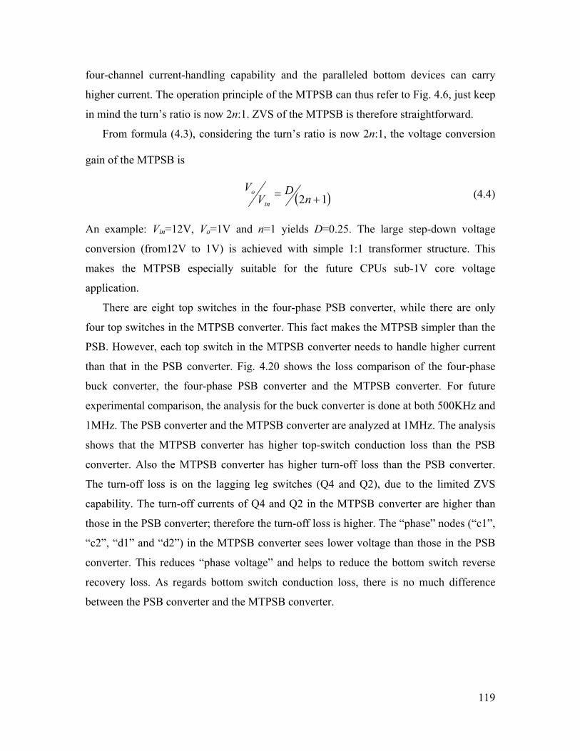
119
four-channel current-handling capability and the paralleled bottom devices can carry
higher current. The operation principle of the MTPSB can thus refer to Fig. 4.6, just keep
in mind the turn’s ratio is now 2n:1. ZVS of the MTPSB is therefore straightforward.
From formula (4.3), considering the turn’s ratio is now 2n:1, the voltage conversion
gain of the MTPSB is
( )12 += nD
VV
in
o (4.4)
An example: Vin=12V, Vo=1V and n=1 yields D=0.25. The large step-down voltage
conversion (from12V to 1V) is achieved with simple 1:1 transformer structure. This
makes the MTPSB especially suitable for the future CPUs sub-1V core voltage
application.
There are eight top switches in the four-phase PSB converter, while there are only
four top switches in the MTPSB converter. This fact makes the MTPSB simpler than the
PSB. However, each top switch in the MTPSB converter needs to handle higher current
than that in the PSB converter. Fig. 4.20 shows the loss comparison of the four-phase
buck converter, the four-phase PSB converter and the MTPSB converter. For future
experimental comparison, the analysis for the buck converter is done at both 500KHz and
1MHz. The PSB converter and the MTPSB converter are analyzed at 1MHz. The analysis
shows that the MTPSB converter has higher top-switch conduction loss than the PSB
converter. Also the MTPSB converter has higher turn-off loss than the PSB converter.
The turn-off loss is on the lagging leg switches (Q4 and Q2), due to the limited ZVS
capability. The turn-off currents of Q4 and Q2 in the MTPSB converter are higher than
those in the PSB converter; therefore the turn-off loss is higher. The “phase” nodes (“c1”,
“c2”, “d1” and “d2”) in the MTPSB converter sees lower voltage than those in the PSB
converter. This reduces “phase voltage” and helps to reduce the bottom switch reverse
recovery loss. As regards bottom switch conduction loss, there is no much difference
between the PSB converter and the MTPSB converter.
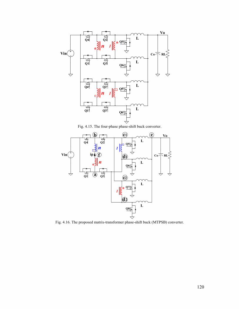
120
Co RL
VoL
L
1 *
Vin
n*Q5Q4
Q1
Q2
Q3 Q6
L
L
1nQ5'Q4'
Q1'
Q2'
Q3' Q6'
Fig. 4.15. The four-phase phase-shift buck converter.
Co RL
VoL
L
1
Vin
n*
b c1
a
d1
e
Q5Q4
Q1
Q2
Q3
Q6
ip
L
L
1 * Q7
Q8
n
c2
d2
f
Fig. 4.16. The proposed matrix-transformer phase-shift buck (MTPSB) converter.

121
Co RL
Vin
VoL
L
L
L
1 1 *b
c1a
c2
e
n
n*
12 +nVin
(a)
Co RL
Vin
VoL
L
L
L
1 1*
a
d1
b
d2
en
n*
12 +nVin
(b)
Fig. 4.17. The equivalent circuits of the matrix-transformer phase-shift buck converter: (a) when Q1 and
Q2 are both on, and (b) when Q3 and Q4 are both on.
Co RL
VoL
L
1 *
Vin
2n*
b c
a d
e
Q5Q4
Q1
Q2
Q3 Q6
L
L
Q7
Q8
Fig. 4.18. The equivalent PSB of the matrix-transformer phase-shift buck converter.
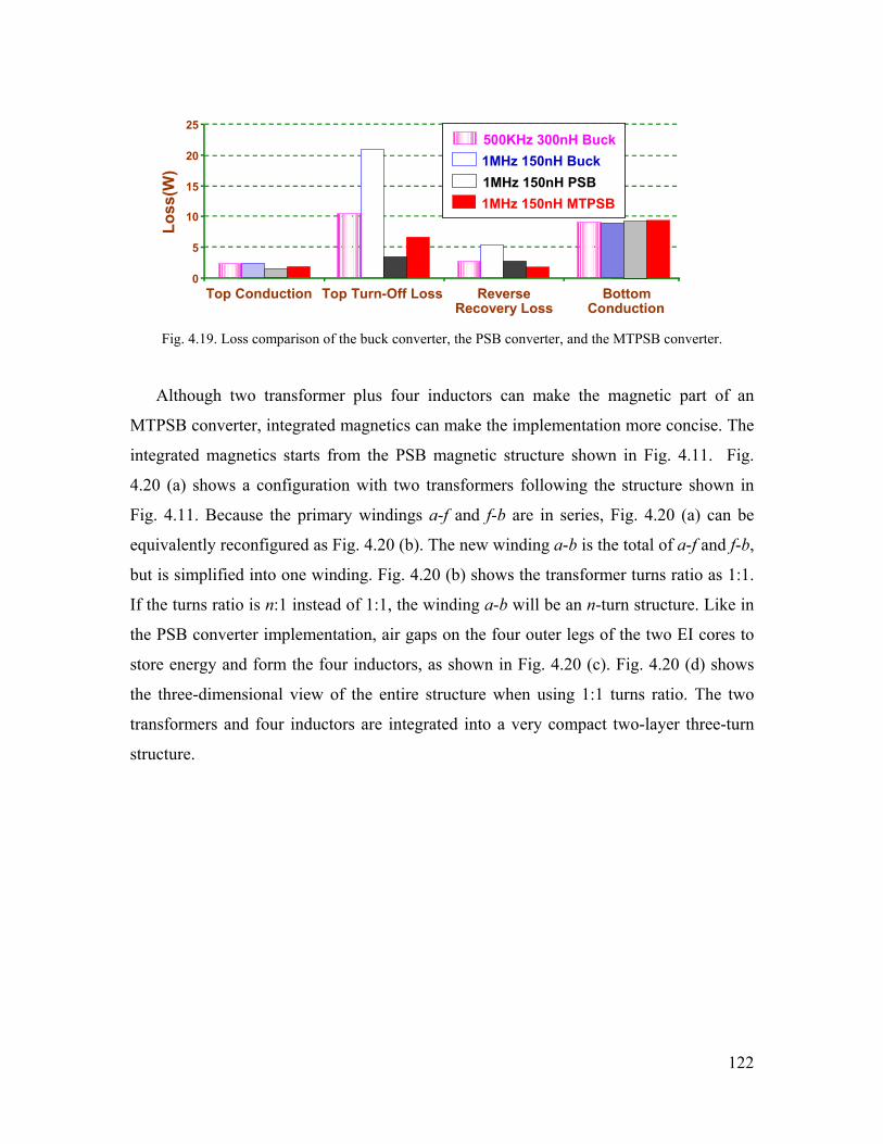
122
0
5
10
15
20
25
Top Conduction Top Turn-Off Loss ReverseRecovery Loss
BottomConduction
Loss
(W)
500KHz 300nH Buck1MHz 150nH Buck1MHz 150nH PSB1MHz 150nH MTPSB
Fig. 4.19. Loss comparison of the buck converter, the PSB converter, and the MTPSB converter.
Although two transformer plus four inductors can make the magnetic part of an
MTPSB converter, integrated magnetics can make the implementation more concise. The
integrated magnetics starts from the PSB magnetic structure shown in Fig. 4.11. Fig.
4.20 (a) shows a configuration with two transformers following the structure shown in
Fig. 4.11. Because the primary windings a-f and f-b are in series, Fig. 4.20 (a) can be
equivalently reconfigured as Fig. 4.20 (b). The new winding a-b is the total of a-f and f-b,
but is simplified into one winding. Fig. 4.20 (b) shows the transformer turns ratio as 1:1.
If the turns ratio is n:1 instead of 1:1, the winding a-b will be an n-turn structure. Like in
the PSB converter implementation, air gaps on the four outer legs of the two EI cores to
store energy and form the four inductors, as shown in Fig. 4.20 (c). Fig. 4.20 (d) shows
the three-dimensional view of the entire structure when using 1:1 turns ratio. The two
transformers and four inductors are integrated into a very compact two-layer three-turn
structure.

123
d1
c1
c2
d2ee
f
b
ee
a
f
(a)
d1
c1
c2
d2e
a
b
(b)
PC Board
Gap
Winding Core
(c)
(d)
Fig. 4.20. The integrated magnetics structure of the matrix-transformer phase-shift buck converter: (a)
Following the PSB implementation, (b) the top view, (c) the air gaps, and (d) the 3-D view.
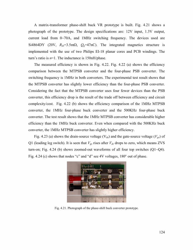
124
A matrix-transformer phase-shift buck VR prototype is built. Fig. 4.21 shows a
photograph of the prototype. The design specifications are: 12V input, 1.3V output,
current load from 0~70A, and 1MHz switching frequency. The devices used are
Si4864DY (20V, Rds=3.5mΩ, Qg=47nC). The integrated magnetics structure is
implemented with the use of two Philips EI-18 planar cores and PCB windings. The
turn’s ratio is n=1. The inductance is 150nH/phase.
The measured efficiency is shown in Fig. 4.22. Fig. 4.22 (a) shows the efficiency
comparison between the MTPSB converter and the four-phase PSB converter. The
switching frequency is 1MHz in both converters. The experimental test result shows that
the MTPSB converter has slightly lower efficiency than the four-phase PSB converter.
Considering the fact that the MTPSB converter uses four fewer devices than the PSB
converter, this efficiency drop is the result of the trade off between efficiency and circuit
complexity/cost. Fig. 4.22 (b) shows the efficiency comparison of the 1MHz MTPSB
converter, the 1MHz four-phase buck converter and the 500KHz four-phase buck
converter. The test result shows that the 1MHz MTPSB converter has considerable higher
efficiency than the 1MHz buck converter. Even when compared with the 500KHz buck
converter, the 1MHz MTPSB converter has slightly higher efficiency.
Fig. 4.23 (a) shows the drain-source voltage (Vds) and the gate-source voltage (Vgs) of
Q1 (leading leg switch). It is seen that Vgs rises after Vds drops to zero, which means ZVS
turn-on; Fig. 4.24 (b) shows zoomed-out waveforms of all four top switches (Q1~Q4).
Fig. 4.24 (c) shows that nodes “c” and “d” see 4V voltages, 180° out of phase.
Fig. 4.21. Photograph of the phase-shift buck converter prototype.
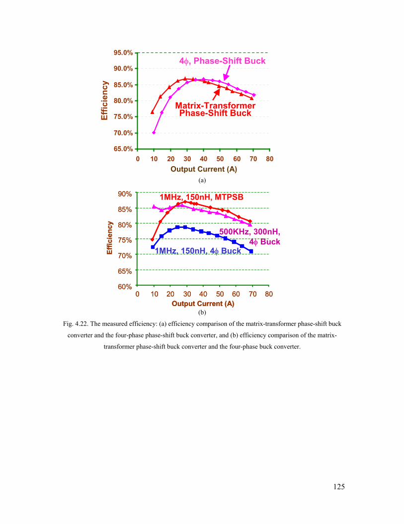
125
65.0%
70.0%
75.0%
80.0%
85.0%
90.0%
95.0%
0 10 20 30 40 50 60 70 80
Effic
ienc
y
4φ, Phase-Shift Buck
Matrix-Transformer Phase-Shift Buck
Output Current (A)
(a)
1MHz, 150nH, 4φ Buck
1MHz, 150nH, MTPSB
500KHz, 300nH, 4φ Buck
Output Current (A)10 20 30 40 50 60 70 800
Output Current (A)10 20 30 40 50 60 70 800
Effic
ienc
y
60%
65%
70%
75%
80%
85%
90%
Effic
ienc
y
60%
65%
70%
75%
80%
85%
90%
(b)
Fig. 4.22. The measured efficiency: (a) efficiency comparison of the matrix-transformer phase-shift buck
converter and the four-phase phase-shift buck converter, and (b) efficiency comparison of the matrix-
transformer phase-shift buck converter and the four-phase buck converter.
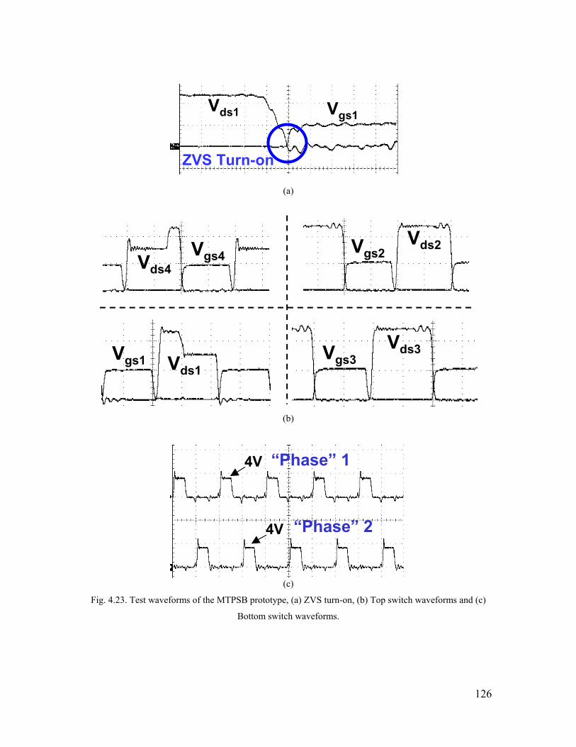
126
Vgs1Vds1
ZVS Turn-on
(a)
Vgs4Vds4
Vgs1 Vds1Vgs3
Vds3
Vgs2Vds2
(b)
4V
4V
“Phase” 1
“Phase” 2
(c)
Fig. 4.23. Test waveforms of the MTPSB prototype, (a) ZVS turn-on, (b) Top switch waveforms and (c)
Bottom switch waveforms.

127
4.5. Cost Benefit of the MTPSB VR Solution.
In Chapter 3, it is concluded that when the switching frequency reaches 1MHz the all-
ceramic solution is better than the OSCON-ceramic solution in terms of both footprint
area and cost, and therefore provides an opportunity to deliver a more cost-effective VR
solution. That being said, the buck converter and the push-pull buck converter cannot
benefit from this solution due to the poor efficiency at 1MHz. However, the emergence of
the MTPSB converter, which is capable of efficient power conversion at 1MHz, makes it
possible to benefit from the all-ceramic solution.
Today’s 12V-input non-isolated VR solution is the multiphase buck converter. The
typical switching frequency is 300~500KHz, and the typical number of phases is four.
There are two major applications for 12V-input non-isolated VRs: one is the desktop
application; the other is the server application. Fig. 4.24 (a) shows the desktop computer
VR solution. In this case, the VR output capacitors are OSCON capacitors plus some
ceramic capacitors. The capacitor design has already been discussed in Chapter 4,
therefore is not explained here. There are eleven OSCON capacitors and 300µF ceramic
capacitor used. Fig. 4.24 (b) shows the server VR solution. In this case, VRs use all
ceramic capacitors for better reliability and low profile, and the amount of ceramic
capacitance is 1600µF. Normally the bottom devices are two MOSFETs in parallel for
efficiency concerns. Fig. 4.25 (a) shows the cost breakdown of the desktop computer VR
design in Fig. 4.24 (a), as of 2002. It can be seen that the capacitor cost is the biggest part
in the total cost. Fig. 4.25 (b) shows the cost breakdown of the server VR design in Fig.
4.25 (b). The cost is normalized based on the desktop computer VR cost. Due to the low
switching frequency (500KHz), the all-ceramic solution is more expensive than the
OSCON-ceramic solution. The shown number is 56% higher.
Fig. 4.24 (c) shows the proposed MTPSB solution. The MTPSB converter operates at
1MHz, and therefore uses only 800µF ceramic capacitors as the output capacitor. Fig.
4.25 (c) shows the cost breakdown of the proposed MTPSB solution. It is very evident
that the capacitor cost is reduced. The high efficiency makes it unnecessary to parallel
devices therefore the device cost is minimal. The additional cost caused by the MTPSB
converter is the cost of the transformers, which is marked as “X” in Fig. 4.25 (c). The
estimation is that the total cost of the MTPSB solution achieves 5% cost reduction
128
compared with the desktop VR solution shown in Fig. 4.24 (a), and 40% cost reduction
compared with the server VR solution shown in Fig. 4.24 (b).
It has already been concluded in Chapter 4 that at 1MHz the all-ceramic solution uses
less footprint area.
Based on the above analysis, it can be concluded that the proposed MTPSB solution
is a more cost-effective solution than today’s multiphase buck solution.

129
Q2Q1
Q4Q3
Q6Q5
Q8Q7
Q2'
Q4'
Q6'
Q8'
Silver Box12VAC Vo=1.3V, Io=70A
CPUCPUfS=500KHz, L=300nH
Needs300µF
#=11
(a)
Q2Q1
Q4Q3
Q6Q5
Q8Q7
Q2'
Q4'
Q6'
Q8'
Silver Box12VAC Vo=1.3V, Io=70A
CPUCPUfS=500KHz, L=300nH
Needs 1600µF
(b)
Silver Box12VAC
1
1*
Q5Q4
Q1
Q2
Q3
Q6
1 * Q7
Q8
1L
L
L
L
Needs 800µF
Vo=1.3V, Io=70A fS=1MHz, L=150nH
CPUCPU
(c)
Fig. 4.24. VR solutions: (a) current desktop computer VR solution, (b) current server VR solution, and
(c) the proposed MTPSB solution.

130
Controlle
rDriv
erUpper
FETs
Lower
FETsAl-E
lec C
in
Ceramic
CoLoutLin
OSCON Co
Controlle
rDriv
erUpper
FETs
Lower
FETsAl-E
lec C
in
Ceramic
CoLoutLin
OSCON Co
Normalized Cost Subtotal=“$1”
(a)
Controlle
rDriv
erUpper
FETsLo
wer FE
TsCer.
Cin
Ceramic Co
LoutLinContro
ller
Driver
Upper FETs
Lower
FETs
Cer. C
in
Ceramic Co
LoutLin
Normalized Cost Subtotal=“$1.56”
(b)
Normalized Cost Subtotal≈“$0.95”
Contro
ller
Driver
Upper
FETs
Lower
FETs
Al-Elec
Cin Cera
mic Co
Lout
Lin
Transfo
rmer
XContro
ller
Driver
Upper
FETs
Lower
FETs
Al-Elec
Cin Cera
mic Co
Lout
Lin
Transfo
rmer
X
(c)
Fig. 4.25. Cost breakdown of the VR solutions: (a) current desktop computer VR solution, (b) current
server VR solution, and (c) the proposed MTPSB solution.

131
4.6. Summary.
High switching frequency reduces the VR output capacitors needed. This benefit is
achieved only when the VR switching frequency is higher than 1MHz. However,
although the PPB converter has good efficiency at 300KHz, its efficiency is still too low
at 1MHz due to the switching loss. Switching loss being a barrier, soft switching is
needed.
The proposed soft-switched phase-shift buck (PSB) converter evolves from the full
bridge converter. With phase-shift control of the top switches, it achieves soft switching
for the top switches. Highly efficient power conversion is achieved at high switching
frequency. The integrated magnetics makes the implementation concise and delivers
good performance.
Given that the PSB converter has good performance, the matrix-transformer phase-
shift buck (MTPSB) converter is a simplified version of the four-phase PSB converter.
The MTPSB converter trades off some performance with circuit complexity. It reduces
the MOSFET count by four compared with the PSB converter while dropping only 1 ~
2% efficiency. This feature establishes itself as a very cost effective solution for future
VRs. The magnetic structure of the MTPSB converter is also very simple with the use of
integrated magnetics.
The proposed matrix-transformer phase-shift buck converter is a more cost-effective
and smaller-size solution than the multiphase buck solution.
132
Chapter 5. The Ultimate Architectural Solution for Future VRs
The Two-Stage Approach
5.1. The Unique Challenges for Laptop VRs.
In Chapter 4, the PSB converter is proposed as a better solution than the 12V-input
multiphase buck converter for desktop application. It is of great interest whether this new
approach can benefit more applications.
Desktop is just one of the two main market segments of personal computers (PCs);
the other is the laptop. Figs. 5.1 and 5.2 show the data from Gartner Dataquest (August
2002). Fig. 5.1 shows the worldwide PC market as of 2002. 77% of the PCs sold are
desktops and 23% are laptops. Fig. 5.2 (a) shows the shipment growth of desktop PCs.
There are 23,575,000 units shipped in the second quarter of 2001, while there are
22,994,000 units shipped in the second quarter of 2002, which is a decline of 2.5%.
Despite the desktop PC market being soft, the laptop PC market is gaining strong growth.
Fig. 5.2 (b) shows the shipment growth of laptop PCs. There are 6,506,000 units shipped
in the second quarter of 2001, while there are 6,901,000 units shipped in the second
quarter of 2002, which translates into 6.1% growth. More recent news indicates that
laptop PCs are expected to oversell desktop PCs in the near future. With laptops gaining
more market share, the research on improving laptop VRs is getting more attention.
Fig. 5.3 shows the power delivery structure of today’s laptop computers. The
electrical power supplied by typical wall outlets supplies 110V alternating current (AC)
voltage to the adapter, which converts the AC voltage into 19V direct current (DC)
voltage. A battery charger draws current from the 19V DC voltage to charge the battery
packs. When AC power is not available, the power selector runs the laptop power from
the batteries.
A laptop CPU VR is used to convert an unregulated high input voltage, either the AC-
DC adapter or battery, to a suitable regulated DC voltage rail to power the core of the
CPU. The state-of-the-art laptop CPU VR solution also uses the multiphase interleaving
synchronous buck topology [1][2][3][4][5][111], as shown in Fig. 5.4, which is the same
as the state-of-the-art desktop VR solution.

133
23%77%
PC Market
Fig. 5.1. The PC market as of year 2002.
Worldwide Non-Mobile PC Unit Shipment Estimates for 2Q02 (Thousands of Units)
2Q01 Shipments 2Q02 Shipments Growth
Total Market 23,575 22,994 -2.5% Source: Gartner Dataquest (July 2002)
(a)
Worldwide Mobile PC Unit Shipment Estimates for 2Q02
(Thousands of Units) 2Q01 Shipments 2Q02 Shipments Growth
Total Market 6,506 6,901 6.1% Source: Gartner Dataquest (August 2002)
(b)
Fig. 5.2. The PC market growth: (a) desktop PCs, and (b) mobile PCs.
19V AC/DCConverter
BatteryCharger
Battery Pack A8.7 - 16.8 Volts Battery Pack B
8.7 - 16.8 Volts
VDC_IN19V
+Vin8.7 - 19V
DecouplingCapacitors
+V_BATTERY8.7 - 16.8V
PowerSelector
CPU VR,DC-DC Convertersand System Loads
Fig. 5.3. Today’s laptop computer power delivery structure.

134
Co RLVin
Q2'Q1
Q3 Q4'
L
L
Q2
Q4
Q3'
Q1'
Fig. 5.4. Today’s laptop VR solution: multiphase buck converter.
Many of the challenges a laptop VR faces are the same as the challenges faced by a
desktop VR. The ever-increasing CPU core current brings the main challenge. Laptops
use mobile CPUs, which have greatly improved in performance in the past few years, just
like their peers in desktops. As they become more powerful, their power consumption has
increased dramatically. Fig. 5.5 shows the current consumption of Intel mobile CPUs. As
the clock frequency increases to 3GHz, the current consumption increases to above 50A.
Just as a desktop VR, a laptop VR needs high efficiency at heavy load to be thermally
alive, and needs to have good transient response. These are the general requirements for a
VR.
Icc
(A)
0
20
40
60
80
100
0 1 2 3 4 50
20
40
60
80
100
0 1 2 3 4 50
20
40
60
80
100
0 1 2 3 4 5
Today
Mobile Processor Clock Freq. (GHz)
Fig. 5.5. Historical data on current consumption of Intel mobile microprocessors.
Laptop VRs have unique challenges that are not raised in desktop VR application.
One of them is the different form-factor. Fig. 5.6 shows a photograph of the CPU VR
solution of IBM Thinkpad A32 laptop computer. It can be seen that the form-factor of a
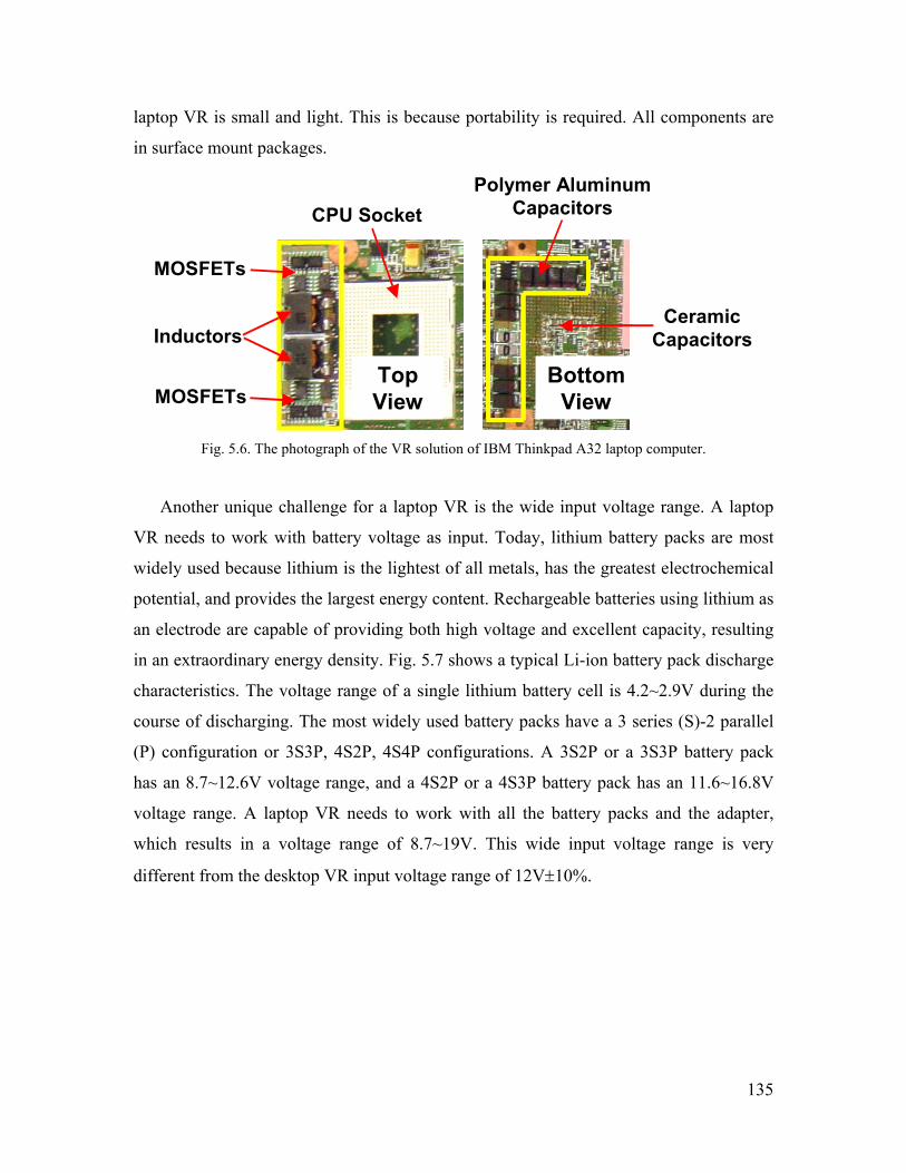
135
laptop VR is small and light. This is because portability is required. All components are
in surface mount packages.
Top ViewTop View
Bottom View
Bottom View
Polymer Aluminum Capacitors
Inductors
MOSFETs
MOSFETs
CPU Socket
Ceramic Capacitors
Fig. 5.6. The photograph of the VR solution of IBM Thinkpad A32 laptop computer.
Another unique challenge for a laptop VR is the wide input voltage range. A laptop
VR needs to work with battery voltage as input. Today, lithium battery packs are most
widely used because lithium is the lightest of all metals, has the greatest electrochemical
potential, and provides the largest energy content. Rechargeable batteries using lithium as
an electrode are capable of providing both high voltage and excellent capacity, resulting
in an extraordinary energy density. Fig. 5.7 shows a typical Li-ion battery pack discharge
characteristics. The voltage range of a single lithium battery cell is 4.2~2.9V during the
course of discharging. The most widely used battery packs have a 3 series (S)-2 parallel
(P) configuration or 3S3P, 4S2P, 4S4P configurations. A 3S2P or a 3S3P battery pack
has an 8.7~12.6V voltage range, and a 4S2P or a 4S3P battery pack has an 11.6~16.8V
voltage range. A laptop VR needs to work with all the battery packs and the adapter,
which results in a voltage range of 8.7~19V. This wide input voltage range is very
different from the desktop VR input voltage range of 12V±10%.

136
A Typical Li-ion Battery Discharge Characteristics (per cell)
2
2.5
3
3.5
4
4.5
TimeVo
ltage
(V)
8
10
12
14
16
Time
Volta
ge (V
)
8
10
12
14
16
TimeVo
ltage
(V)
4S2P Battery Pack 3S2P Battery Pack
Fig. 5.7. Li-ion battery pack discharge characteristics.
Laptops are constrained by battery life. Laptop users often work on the road, which
means the battery is the only energy source available. It is very important to reduce the
power consumption of the entire laptop platform to prolong battery life. Fig. 5.8 shows
the base power scenario of a laptop platform running a battery life benchmark ZDBL4.01
(Ziff Davis BL4.01) [111]. This is a high power scenario and the LCD display is not
included in this pie chart. The biggest power consumer is the CPU. It accounts for 57% of
the base power. The second biggest part is the power supply loss, which accounts for
14% of the base power. All the other components account for 29% of the base power.
To reduce the biggest part of the power pie, mobile CPUs use aggressive power
management; the CPU frequently goes into sleep states. This can even happen between
keystrokes. Fig. 5.9 shows an example of mobile CPU power consumption profile. When
the CPU is performing instructions, it is in the high power state (C0) and draws high
current from the VR; for the rest of the time, it is in the sleep power states and draws low
current. There are multiple sleep power states, sleep state (C1), deep sleep state (C2), etc.
By entering the sleep power states, the CPU consumes less average power. How often the
CPU is in the peak power state determines what the average CPU power is, and this is
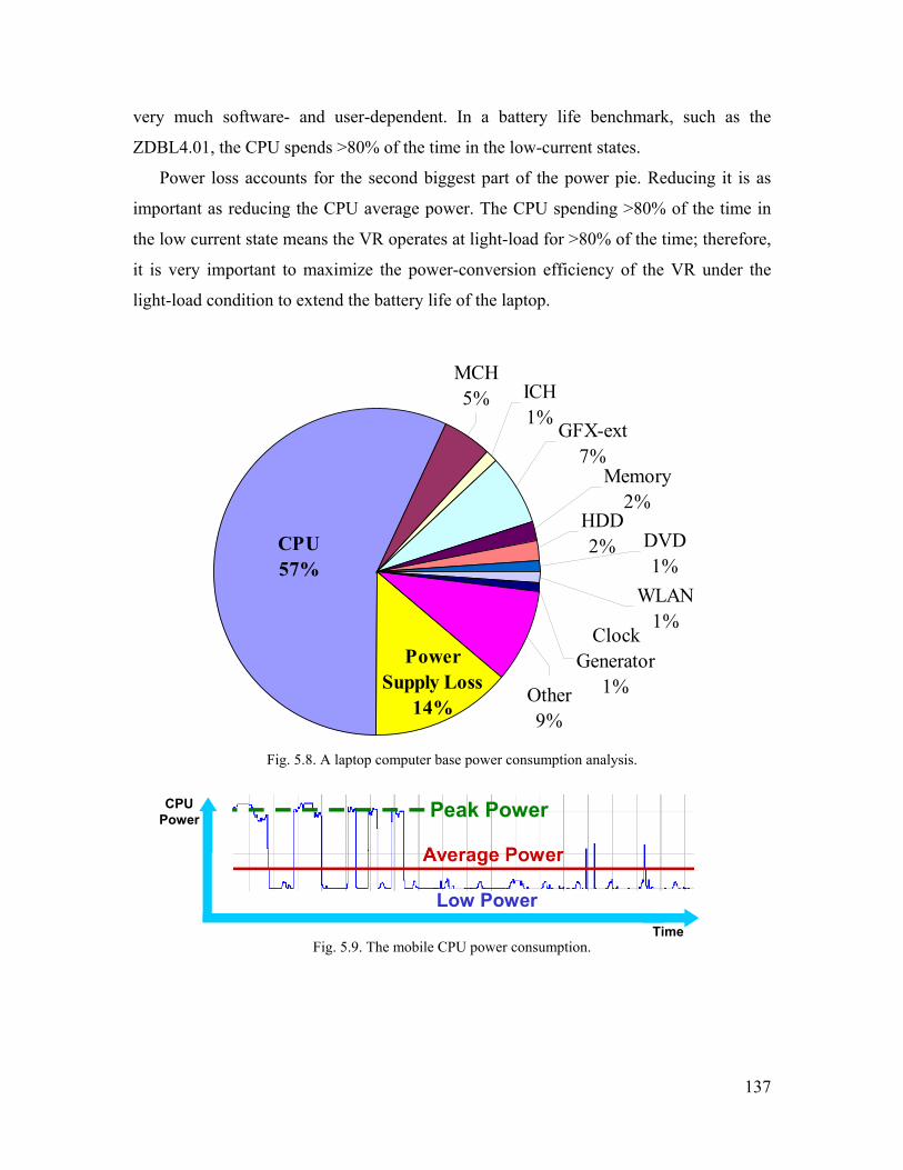
137
very much software- and user-dependent. In a battery life benchmark, such as the
ZDBL4.01, the CPU spends >80% of the time in the low-current states.
Power loss accounts for the second biggest part of the power pie. Reducing it is as
important as reducing the CPU average power. The CPU spending >80% of the time in
the low current state means the VR operates at light-load for >80% of the time; therefore,
it is very important to maximize the power-conversion efficiency of the VR under the
light-load condition to extend the battery life of the laptop.
ClockGenerator
1%Other9%
WLAN1%
PowerSupply Loss
14%
CPU57%
MCH5% ICH
1%
DVD1%
HDD2%
Memory2%
GFX-ext7%
Fig. 5.8. A laptop computer base power consumption analysis.
Peak Power
Time
CPUPower
Low Power
Fig. 5.9. The mobile CPU power consumption.
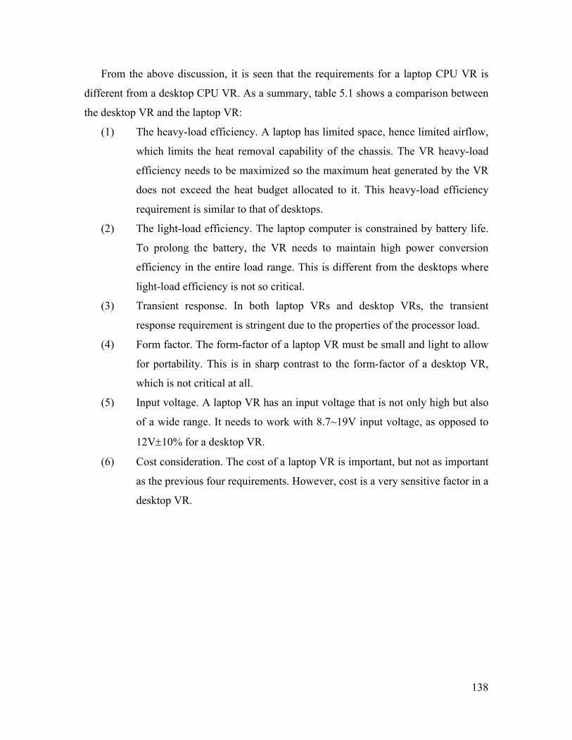
138
From the above discussion, it is seen that the requirements for a laptop CPU VR is
different from a desktop CPU VR. As a summary, table 5.1 shows a comparison between
the desktop VR and the laptop VR:
(1) The heavy-load efficiency. A laptop has limited space, hence limited airflow,
which limits the heat removal capability of the chassis. The VR heavy-load
efficiency needs to be maximized so the maximum heat generated by the VR
does not exceed the heat budget allocated to it. This heavy-load efficiency
requirement is similar to that of desktops.
(2) The light-load efficiency. The laptop computer is constrained by battery life.
To prolong the battery, the VR needs to maintain high power conversion
efficiency in the entire load range. This is different from the desktops where
light-load efficiency is not so critical.
(3) Transient response. In both laptop VRs and desktop VRs, the transient
response requirement is stringent due to the properties of the processor load.
(4) Form factor. The form-factor of a laptop VR must be small and light to allow
for portability. This is in sharp contrast to the form-factor of a desktop VR,
which is not critical at all.
(5) Input voltage. A laptop VR has an input voltage that is not only high but also
of a wide range. It needs to work with 8.7~19V input voltage, as opposed to
12V±10% for a desktop VR.
(6) Cost consideration. The cost of a laptop VR is important, but not as important
as the previous four requirements. However, cost is a very sensitive factor in a
desktop VR.
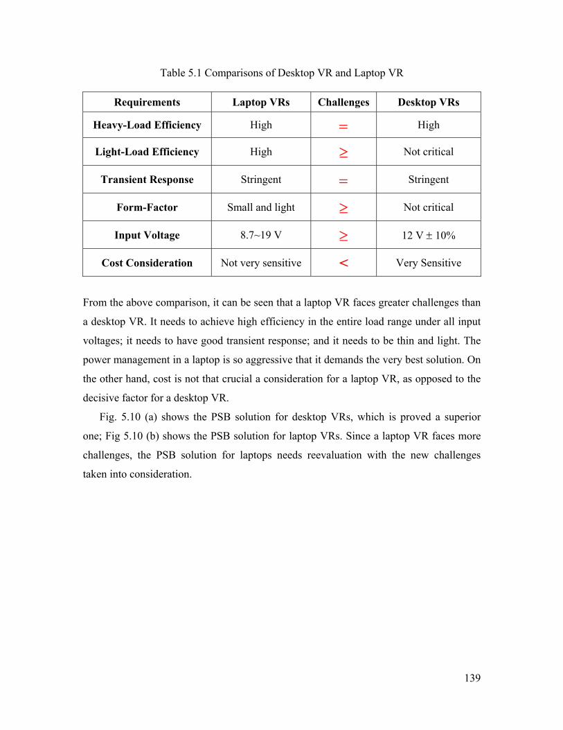
139
Table 5.1 Comparisons of Desktop VR and Laptop VR
Requirements Laptop VRs Challenges Desktop VRs
Heavy-Load Efficiency High = High
Light-Load Efficiency High ≥ Not critical
Transient Response Stringent = Stringent
Form-Factor Small and light ≥ Not critical
Input Voltage 8.7~19 V ≥ 12 V ± 10%
Cost Consideration Not very sensitive < Very Sensitive
From the above comparison, it can be seen that a laptop VR faces greater challenges than
a desktop VR. It needs to achieve high efficiency in the entire load range under all input
voltages; it needs to have good transient response; and it needs to be thin and light. The
power management in a laptop is so aggressive that it demands the very best solution. On
the other hand, cost is not that crucial a consideration for a laptop VR, as opposed to the
decisive factor for a desktop VR.
Fig. 5.10 (a) shows the PSB solution for desktop VRs, which is proved a superior
one; Fig 5.10 (b) shows the PSB solution for laptop VRs. Since a laptop VR faces more
challenges, the PSB solution for laptops needs reevaluation with the new challenges
taken into consideration.
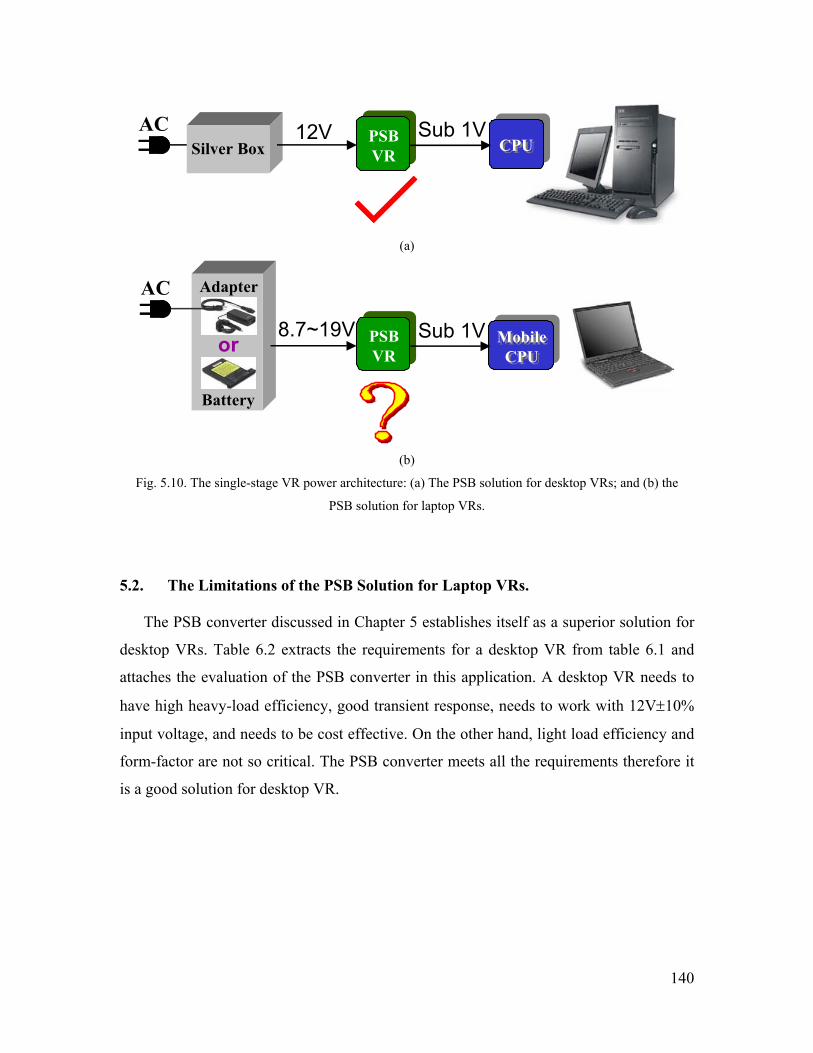
140
Silver Box12VAC PSB
VRSub 1V
CPUCPU
(a)
8.7~19V Sub 1V Mobile CPU
Mobile CPU
Adapter
Battery
or
AC
PSBVR
(b)
Fig. 5.10. The single-stage VR power architecture: (a) The PSB solution for desktop VRs; and (b) the
PSB solution for laptop VRs.
5.2. The Limitations of the PSB Solution for Laptop VRs.
The PSB converter discussed in Chapter 5 establishes itself as a superior solution for
desktop VRs. Table 6.2 extracts the requirements for a desktop VR from table 6.1 and
attaches the evaluation of the PSB converter in this application. A desktop VR needs to
have high heavy-load efficiency, good transient response, needs to work with 12V±10%
input voltage, and needs to be cost effective. On the other hand, light load efficiency and
form-factor are not so critical. The PSB converter meets all the requirements therefore it
is a good solution for desktop VR.
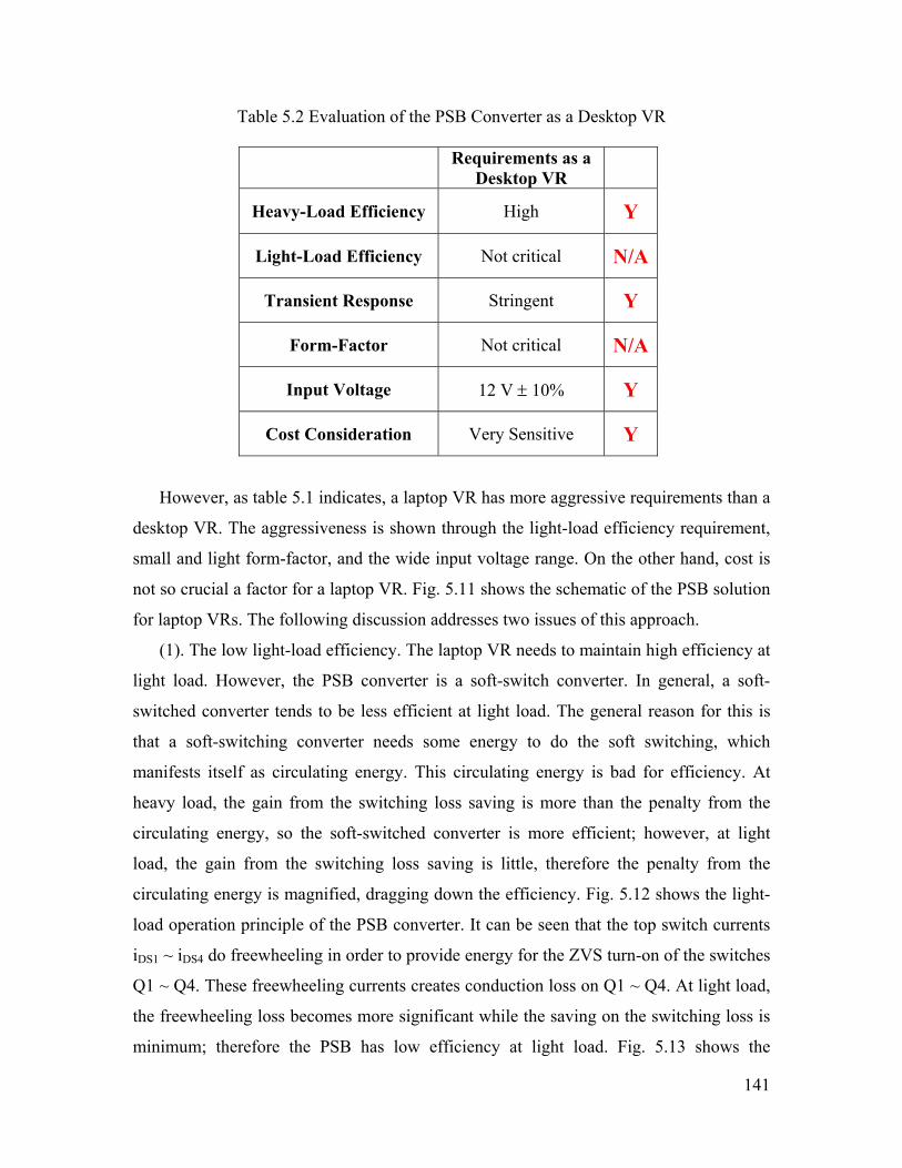
141
Table 5.2 Evaluation of the PSB Converter as a Desktop VR
Requirements as a Desktop VR
Heavy-Load Efficiency High Y
Light-Load Efficiency Not critical N/A
Transient Response Stringent Y
Form-Factor Not critical N/A
Input Voltage 12 V ± 10% Y
Cost Consideration Very Sensitive Y
However, as table 5.1 indicates, a laptop VR has more aggressive requirements than a
desktop VR. The aggressiveness is shown through the light-load efficiency requirement,
small and light form-factor, and the wide input voltage range. On the other hand, cost is
not so crucial a factor for a laptop VR. Fig. 5.11 shows the schematic of the PSB solution
for laptop VRs. The following discussion addresses two issues of this approach.
(1). The low light-load efficiency. The laptop VR needs to maintain high efficiency at
light load. However, the PSB converter is a soft-switch converter. In general, a soft-
switched converter tends to be less efficient at light load. The general reason for this is
that a soft-switching converter needs some energy to do the soft switching, which
manifests itself as circulating energy. This circulating energy is bad for efficiency. At
heavy load, the gain from the switching loss saving is more than the penalty from the
circulating energy, so the soft-switched converter is more efficient; however, at light
load, the gain from the switching loss saving is little, therefore the penalty from the
circulating energy is magnified, dragging down the efficiency. Fig. 5.12 shows the light-
load operation principle of the PSB converter. It can be seen that the top switch currents
iDS1 ~ iDS4 do freewheeling in order to provide energy for the ZVS turn-on of the switches
Q1 ~ Q4. These freewheeling currents creates conduction loss on Q1 ~ Q4. At light load,
the freewheeling loss becomes more significant while the saving on the switching loss is
minimum; therefore the PSB has low efficiency at light load. Fig. 5.13 shows the
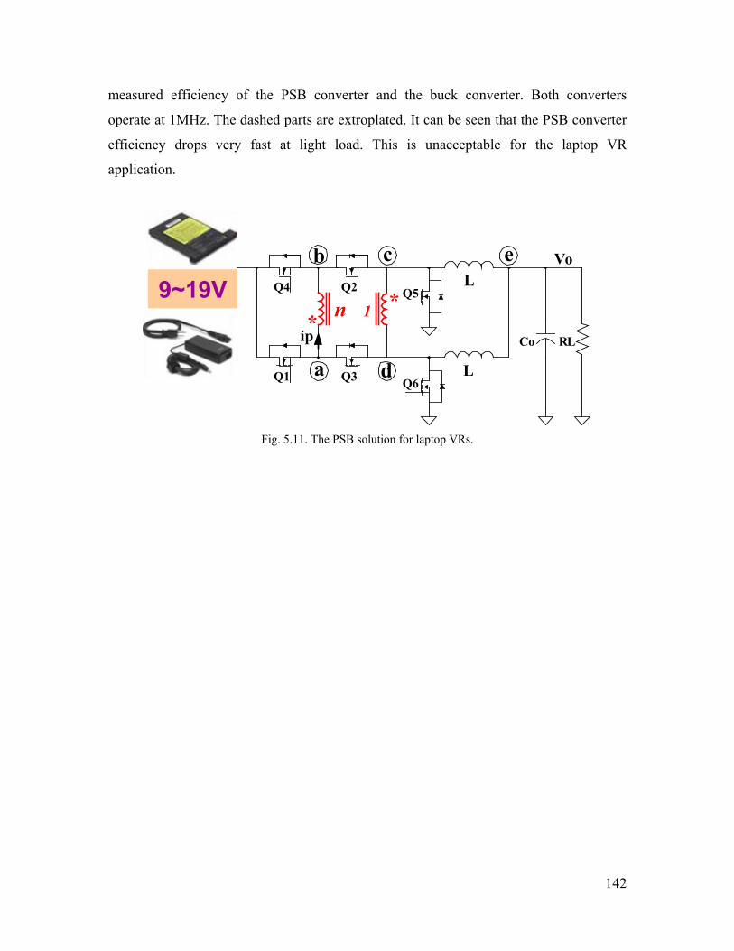
142
measured efficiency of the PSB converter and the buck converter. Both converters
operate at 1MHz. The dashed parts are extroplated. It can be seen that the PSB converter
efficiency drops very fast at light load. This is unacceptable for the laptop VR
application.
Co RL
VoL
L
1 *n*
b c
a d
e
Q5Q4
Q1
Q2
Q3 Q6
ip
9~19V
Fig. 5.11. The PSB solution for laptop VRs.
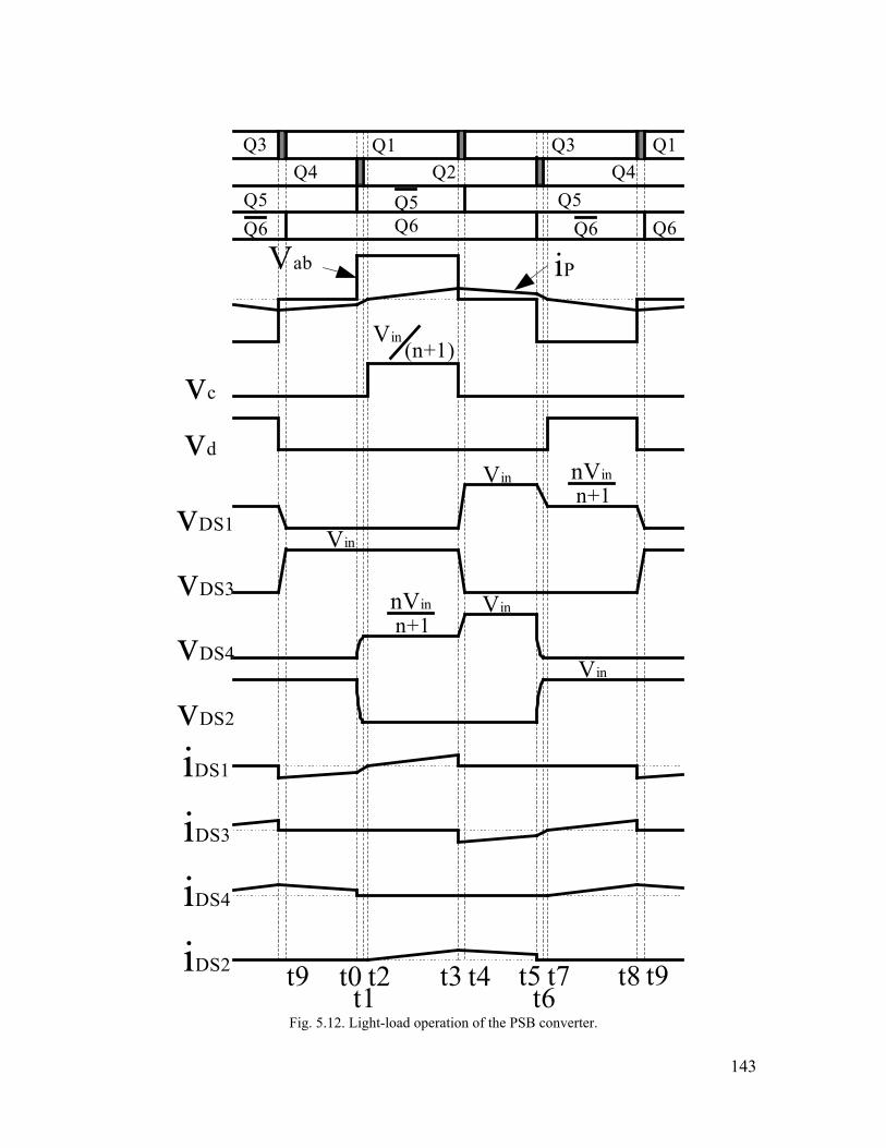
143
Q1 Q3Q4 Q2 Q4
Vab iP
vc
vd
vDS1
vDS3
vDS4
vDS2
iDS1
iDS3
iDS4
iDS2
Q5Q5Q6 Q6Q5
Q6
Q3 Q1
Q6
t0t1
t3 t5 t7 t8t9
Vin(n+1)
nVinn+1
Vin
Vin
Vin
Vin
nVin
n+1
t4 t9t2t6
Fig. 5.12. Light-load operation of the PSB converter.
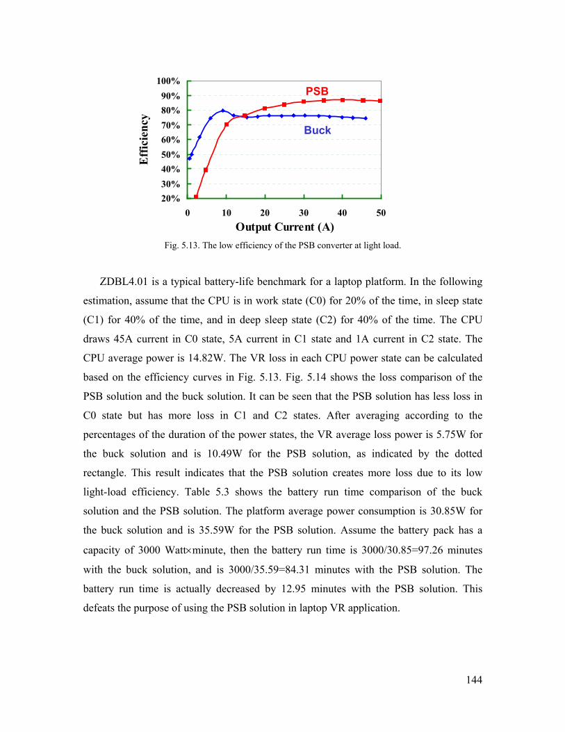
144
20%30%40%50%60%70%80%90%
100%
0 10 20 30 40 50Output Current (A)
Eff
icie
ncy
Buck
PSB
Fig. 5.13. The low efficiency of the PSB converter at light load.
ZDBL4.01 is a typical battery-life benchmark for a laptop platform. In the following
estimation, assume that the CPU is in work state (C0) for 20% of the time, in sleep state
(C1) for 40% of the time, and in deep sleep state (C2) for 40% of the time. The CPU
draws 45A current in C0 state, 5A current in C1 state and 1A current in C2 state. The
CPU average power is 14.82W. The VR loss in each CPU power state can be calculated
based on the efficiency curves in Fig. 5.13. Fig. 5.14 shows the loss comparison of the
PSB solution and the buck solution. It can be seen that the PSB solution has less loss in
C0 state but has more loss in C1 and C2 states. After averaging according to the
percentages of the duration of the power states, the VR average loss power is 5.75W for
the buck solution and is 10.49W for the PSB solution, as indicated by the dotted
rectangle. This result indicates that the PSB solution creates more loss due to its low
light-load efficiency. Table 5.3 shows the battery run time comparison of the buck
solution and the PSB solution. The platform average power consumption is 30.85W for
the buck solution and is 35.59W for the PSB solution. Assume the battery pack has a
capacity of 3000 Watt×minute, then the battery run time is 3000/30.85=97.26 minutes
with the buck solution, and is 3000/35.59=84.31 minutes with the PSB solution. The
battery run time is actually decreased by 12.95 minutes with the PSB solution. This
defeats the purpose of using the PSB solution in laptop VR application.

145
0
5
10
15
20
25
Los
s (W
)
Single Stage BuckPSB
VR Loss in C0
(Work State)VR Loss in C1
(Sleep State)
VR Loss in C2
(Deep Sleep State)
VR Average Loss
Fig. 5.14. Loss comparison of the buck solution and the PSB solution.
Table 5.3. Battery Run Time Comparison of the Buck Solution and the
PSB Solution
Buck VR Solution PSB VR Solution
CPU Average Power (W) 14.82 14.82
CPU VR Average Loss (W) 5.75 10.49
Platform Average Power (W) 30.85 35.59
Battery Capacity (W×m) 3000 3000
Battery Run Time (m) 97.26 84.31
(2). The wide input voltage range. The voltage gain of the PSB converter is
1+=
nD
VV
in
o (5.1)
where D is the duty cycle, n is the transformer turns ratio, Vo is 1.3V, and Vin has a range
of 8.7~19V. Because of the Vin range, the duty cycle has a range too. Using n=2 as an
example, the voltage gain versus duty cycle is plotted in Fig. 5.15. The duty cycle ranges
from 0.2 to 0.45. The wide duty cycle range is problematic. To be able to work with the
high input voltage, a small n has to be used. However, it is not desirable to use a small
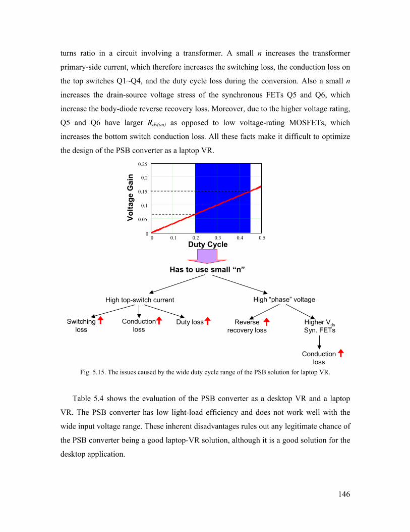
146
turns ratio in a circuit involving a transformer. A small n increases the transformer
primary-side current, which therefore increases the switching loss, the conduction loss on
the top switches Q1~Q4, and the duty cycle loss during the conversion. Also a small n
increases the drain-source voltage stress of the synchronous FETs Q5 and Q6, which
increase the body-diode reverse recovery loss. Moreover, due to the higher voltage rating,
Q5 and Q6 have larger Rds(on) as opposed to low voltage-rating MOSFETs, which
increases the bottom switch conduction loss. All these facts make it difficult to optimize
the design of the PSB converter as a laptop VR.
0 0.1 0.2 0.3 0.4 0.50
0.05
0.1
0.15
0.2
0.25
Volta
ge G
ain
Duty Cycle
Has to use small “n”
High top-switch current High “phase” voltage
Conduction loss
Switching loss
Duty loss Reverse recovery loss
Higher VdsSyn. FETs
Conduction loss
Fig. 5.15. The issues caused by the wide duty cycle range of the PSB solution for laptop VR.
Table 5.4 shows the evaluation of the PSB converter as a desktop VR and a laptop
VR. The PSB converter has low light-load efficiency and does not work well with the
wide input voltage range. These inherent disadvantages rules out any legitimate chance of
the PSB converter being a good laptop-VR solution, although it is a good solution for the
desktop application.

147
Table 5.4 Evaluation of the PSB Converter as a Desktop VR and a Laptop VR
Requirements as a Desktop VR Requirements as a
Laptop VR
Heavy-Load Efficiency High Y High Y
Light-Load Efficiency Not critical N/A High N
Transient Response Stringent Y Stringent Y
Form-Factor Not critical N/A Small and light Y
Input Voltage 12 V ± 10% Y 8.7~19 V N
Cost Consideration Very Sensitive Y Not very sensitive N/A
Wide input-voltage range is not a stranger to many applications. Other researchers
have done much valuable work in dealing with wide input voltage range. There are
different ways to do design trade-offs with wide input-voltage range. References [76] ~
[80] present some method used to deal with wide input voltage range in AC-DC
applications; references [81] ~ [93] present some method used in DC-DC applications.
On the other hand, the two-stage architecture is another attractive solution. References
[94] ~ [97] present the two-stage approach to get an efficient system with wide input-
voltage range. All of these are valuable tips for finding a better solution for laptop VRs.
The two-stage approach is of further interest because references [99] and [100] show
that the two-stage approach is also an attractive solution for desktop VRs. Fig. 5.16
shows the schematic of the two-stage VR. The first stage is a low-frequency two-phase
buck converter, converting the input voltage to an intermediate bus voltage Vbus; the
second stage is a high-frequency multiphase buck converter, converting Vbus to the CPU
core voltage. Fig. 5.17 shows the efficiency achieved in reference [100]. It is seen that the
two-stage solution achieves high efficiency at high switching frequency.
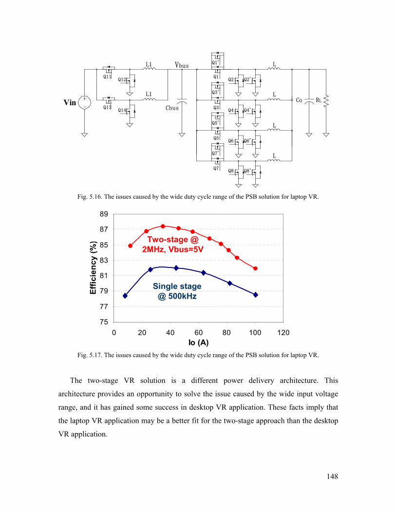
148
Co RLVin
Q2'Q1
Q3Q4'
L
L
Q6'Q5
Q7 Q8'
L
L
Q2
Q4
Q6
Q8
Q5'
Q3'
Q1'
Q7'
Cbus
Q11
Q13
L1
L1
Q12
Q14
Vbus
Fig. 5.16. The issues caused by the wide duty cycle range of the PSB solution for laptop VR.
75
77
79
81
83
85
87
89
0 20 40 60 80 100 120Io (A)
Effic
ienc
y (%
)
Single stage @ 500kHz
Two-stage @ 2MHz, Vbus=5V
Fig. 5.17. The issues caused by the wide duty cycle range of the PSB solution for laptop VR.
The two-stage VR solution is a different power delivery architecture. This
architecture provides an opportunity to solve the issue caused by the wide input voltage
range, and it has gained some success in desktop VR application. These facts imply that
the laptop VR application may be a better fit for the two-stage approach than the desktop
VR application.

149
5.3. Benefits of the the Two-Stage Approach.
Fig. 5.18 shows the measured efficiency of a buck VR operating at 1MHz switching
frequency and different input voltages. It can be observed that when the input voltage is
low, the buck VR is very efficient. For example, the efficiency is still over 90% when the
input voltage is 5V. This fact indicates that a low-input voltage high frequency buck VR
can be very efficient, and this is the foundation of the viability of the two-stage approach.
70%
75%
80%
85%
90%
0 5 10 15 20 25 30 35Output Current (A)
95%
100%
Effic
ienc
y
Vin=9VVin=16V
Vin=19V
Vin=5V
Fig. 5.18. The buck VR has high efficiency at high frequency when the input voltage is low.
Fig. 5.19 shows the proposed two-stage laptop VR. In this structure, the two stages
are optimized for different purposes. The second-stage multiphase buck converter focuses
on achieving high efficiency at high switching frequency; therefore the output capacitors
are greatly reduced. This has been proven possible when a low Vbus is chosen. As to the
first stage, the main tasks are to handle the wide input-voltage range and to create the bus
voltage Vbus efficiently under all input voltage conditions.
In order to get high efficiency, the first stage operates at a low switching frequency.
Also because Vbus is much higher than the CPU core voltage, the first-stage duty cycle is
pretty large. Moreover, since Vbus does not have stringent transient response requirement,
fairly large inductance can be used in the first-stage buck converter. With low switching
frequency, pretty large duty cycle and large inductance, it is very possible for the first
stage to get high efficiency under all input voltage conditions. Therefore, it is possible
that cascading these two stages provides a more efficient high-frequency solution.
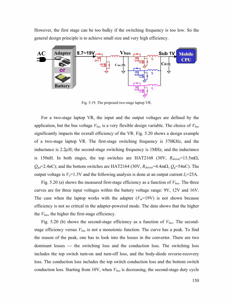
150
However, the first stage can be too bulky if the switching frequency is too low. So the
general design principle is to achieve small size and very high efficiency.
8.7~19V Sub 1V Mobile CPU
Mobile CPU
Adapter
Battery
or
AC
C busQ12Q11
CoQ2Q1
Q4Q3
Q6Q5
L
L
L
Vbus
Fig. 5.19. The proposed two-stage laptop VR.
For a two-stage laptop VR, the input and the output voltages are defined by the
application, but the bus voltage Vbus is a very flexible design variable. The choice of Vbus
significantly impacts the overall efficiency of the VR. Fig. 5.20 shows a design example
of a two-stage laptop VR. The first-stage switching frequency is 370KHz, and the
inductance is 2.2µH; the second-stage switching frequency is 1MHz, and the inductance
is 150nH. In both stages, the top switches are HAT2168 (30V, Rds(on)=13.5mΩ,
Qgd=2.4nC); and the bottom switches are HAT2164 (30V, Rds(on)=4.4mΩ, Qg=54nC). The
output voltage is Vo=1.3V and the following analysis is done at an output current Io=25A.
Fig. 5.20 (a) shows the measured first-stage efficiency as a function of Vbus. The three
curves are for three input voltages within the battery voltage range: 9V, 12V and 16V.
The case when the laptop works with the adapter (Vin=19V) is not shown because
efficiency is not so critical in the adapter-powered mode. The data shows that the higher
the Vbus, the higher the first-stage efficiency.
Fig. 5.20 (b) shows the second-stage efficiency as a function of Vbus. The second-
stage efficiency versus Vbus is not a monotonic function. The curve has a peak. To find
the reason of the peak, one has to look into the losses in the converter. There are two
dominant losses the switching loss and the conduction loss. The switching loss
includes the top switch turn-on and turn-off loss, and the body-diode reverse-recovery
loss. The conduction loss includes the top switch conduction loss and the bottom switch
conduction loss. Starting from 10V, when Vbus is decreasing, the second-stage duty cycle
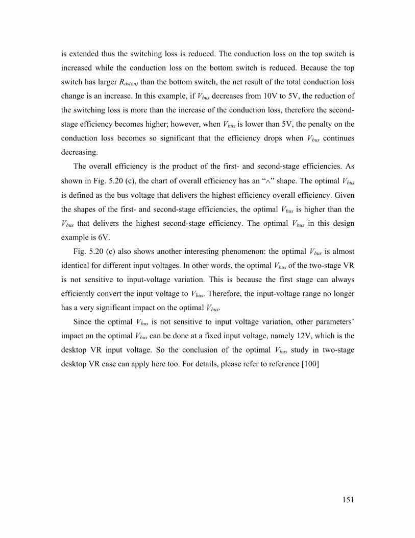
151
is extended thus the switching loss is reduced. The conduction loss on the top switch is
increased while the conduction loss on the bottom switch is reduced. Because the top
switch has larger Rds(on) than the bottom switch, the net result of the total conduction loss
change is an increase. In this example, if Vbus decreases from 10V to 5V, the reduction of
the switching loss is more than the increase of the conduction loss, therefore the second-
stage efficiency becomes higher; however, when Vbus is lower than 5V, the penalty on the
conduction loss becomes so significant that the efficiency drops when Vbus continues
decreasing.
The overall efficiency is the product of the first- and second-stage efficiencies. As
shown in Fig. 5.20 (c), the chart of overall efficiency has an “∧” shape. The optimal Vbus
is defined as the bus voltage that delivers the highest efficiency overall efficiency. Given
the shapes of the first- and second-stage efficiencies, the optimal Vbus is higher than the
Vbus that delivers the highest second-stage efficiency. The optimal Vbus in this design
example is 6V.
Fig. 5.20 (c) also shows another interesting phenomenon: the optimal Vbus is almost
identical for different input voltages. In other words, the optimal Vbus of the two-stage VR
is not sensitive to input-voltage variation. This is because the first stage can always
efficiently convert the input voltage to Vbus. Therefore, the input-voltage range no longer
has a very significant impact on the optimal Vbus.
Since the optimal Vbus is not sensitive to input voltage variation, other parameters’
impact on the optimal Vbus can be done at a fixed input voltage, namely 12V, which is the
desktop VR input voltage. So the conclusion of the optimal Vbus study in two-stage
desktop VR case can apply here too. For details, please refer to reference [100]
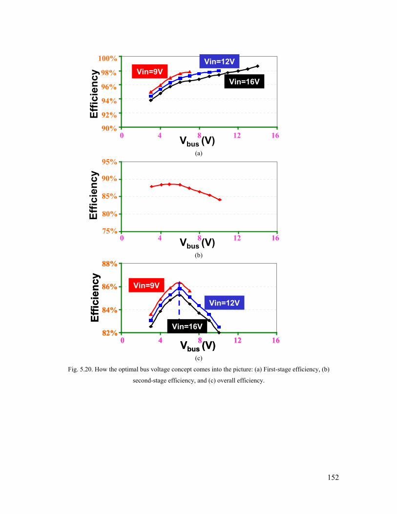
152
Vbus (V)0 4 8 12 16
92%
94%
96%
98%
100%
90%
Effic
ienc
yVin=16V
Vin=12VVin=9V
(a)
Vbus (V)0 4 8 12 1675%
80%
85%
90%
95%
Effic
ienc
y
(b)
Vbus (V)0 4 8 12 16
Effic
ienc
y
82%
84%
86%
88%
Vbus (V)0 4 8 12 16
Effic
ienc
y
82%
84%
86%
88%
Vin=12V
Vin=9V
Vin=16V
(c)
Fig. 5.20. How the optimal bus voltage concept comes into the picture: (a) First-stage efficiency, (b)
second-stage efficiency, and (c) overall efficiency.
153
Presently single-stage laptops VRs use 30V devices because they have to work with
an input voltage up to 19V. Lower voltage-rating devices have smaller FOMs than 30V
devices, and smaller FOMs mean better devices and potentially better performance.
Unfortunately the single-stage buck VR cannot benefit from this fact. For a two-stage
laptop VR, the second-stage buck converter works with Vbus as the input voltage, and
since Vbus is lower than Vin, low voltage-rating devices can be used instead of 30V
MOSFETs.
Two experimental tests are done at 1.3V/25A output. One uses 30V MOSFETs and
the other uses 20V MOSFETs as the second-stage bottom switches. The first stage is the
same: The top switch is HAT2168, the bottom switch is HAT2164, the switching
frequency is 370KHz, and the inductance is 2.2µH. Fig. 5.21 (a) shows the measured
first-stage efficiency as a function of Vbus. Fig. 5.21 (b) shows the measured second-stage
efficiency as a function of Vbus. The bottom curve is measured when HAT2164 (30V,
FOM=180mΩ·nC) is used as the bottom switches. The top curve is measured when
Si4864 (20V, FOM=130mΩ·nC) is used as the bottom switches. It is clearly shown that
the second-stage efficiency benefits from the small-FOM 20V devices. Fig. 5.21 (c)
shows the overall efficiency. The optimal Vbus is 6V and the efficiency is 2% higher using
20V MOSFETs than using 30V MOSFETs.
154
90%
92%
94%
96%
98%
100%
0 2 4 6 8 10 12 14 16Vbus
Effic
ienc
y
(a)
75%
80%
85%
90%
95%
0 2 4 6 8 10 12 14 1675%
80%
85%
90%
95%
0 2 4 6 8 10 12 14 16Vbus
Bottom: HAT2164(30V)Bottom: HAT2164(30V)
Bottom: Si4864(20V)Bottom: Si4864(20V)
Io=25A
Effic
ienc
y
(b)
75%
80%
85%
90%
0 2 4 6 8 10 12 14 1675%
80%
85%
90%
0 2 4 6 8 10 12 14 16Vbus
30V FETs30V FETs
20V FETs20V FETs
Effic
ienc
y
(c)
Fig. 5.21. The two-stage VR can benefit from low voltage-rating devices: (a) first-stage efficiency, (b)
second-stage efficiency, and (c) overall efficiency.
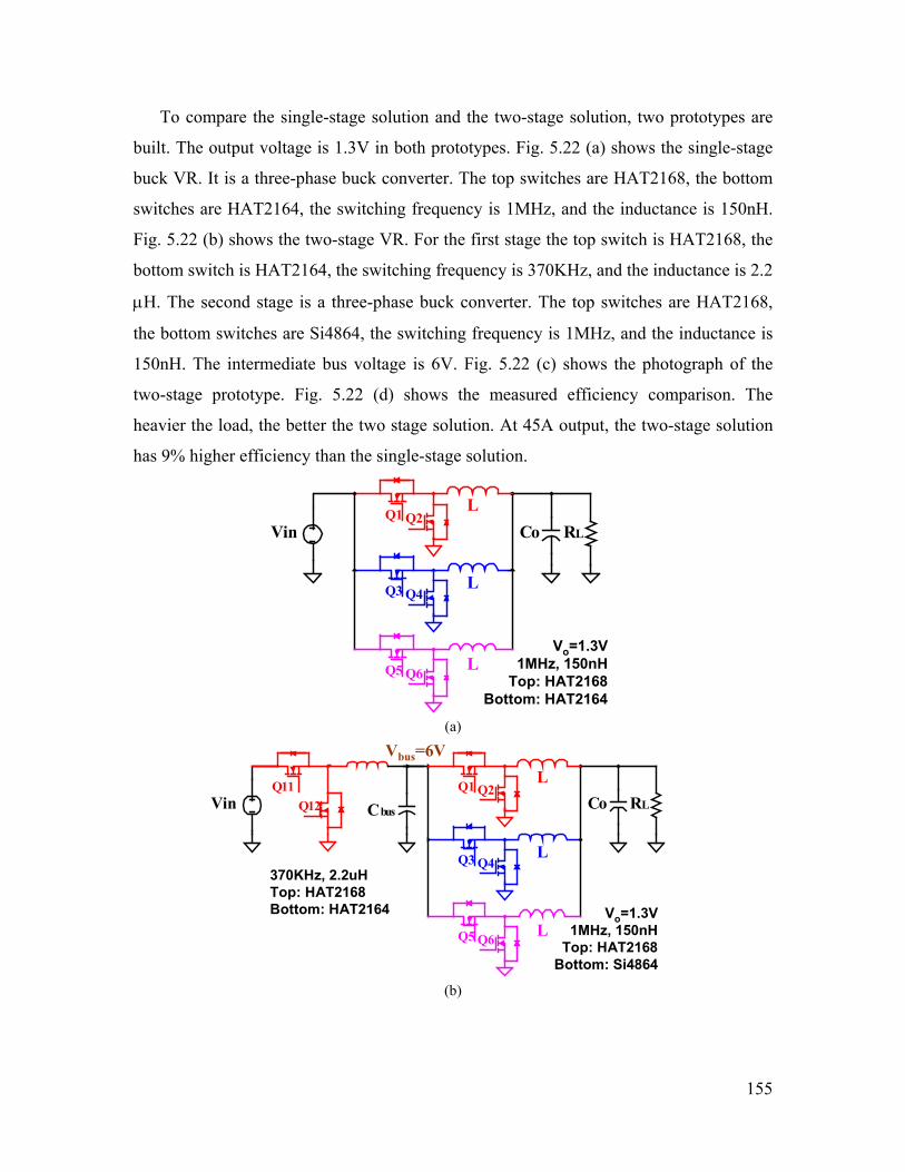
155
To compare the single-stage solution and the two-stage solution, two prototypes are
built. The output voltage is 1.3V in both prototypes. Fig. 5.22 (a) shows the single-stage
buck VR. It is a three-phase buck converter. The top switches are HAT2168, the bottom
switches are HAT2164, the switching frequency is 1MHz, and the inductance is 150nH.
Fig. 5.22 (b) shows the two-stage VR. For the first stage the top switch is HAT2168, the
bottom switch is HAT2164, the switching frequency is 370KHz, and the inductance is 2.2
µH. The second stage is a three-phase buck converter. The top switches are HAT2168,
the bottom switches are Si4864, the switching frequency is 1MHz, and the inductance is
150nH. The intermediate bus voltage is 6V. Fig. 5.22 (c) shows the photograph of the
two-stage prototype. Fig. 5.22 (d) shows the measured efficiency comparison. The
heavier the load, the better the two stage solution. At 45A output, the two-stage solution
has 9% higher efficiency than the single-stage solution.
Co RLQ2Q1
Q4Q3
Q6Q5
L
L
L
Vin
Vo=1.3V1MHz, 150nH
Top: HAT2168Bottom: HAT2164
(a)
Co RLQ2Q1
Q4Q3
Q6Q5
L
L
L
C busVin Q12Q11
Vbus=6V
370KHz, 2.2uHTop: HAT2168Bottom: HAT2164 Vo=1.3V
1MHz, 150nHTop: HAT2168
Bottom: Si4864
(b)

156
(c)
10 20 30 40 50Output Current(A)
50%
60%
70%
80%
90%
0
Effic
ienc
y 9%9%9%1MHz Two-Stage
1MHz Single-Stage
(With Gate Drive Loss)
(d)
Fig. 5.22. The efficiency comparison of the two-stage solution and the single-stage solution: (a) the
single-stage solution, (b) the two-stage solution, (c) the photograph of the two-stage VR prototype, and
(d) the measured efficiency comparison.
Fig. 5.23 shows the loss comparison of the buck solution and the two-stage solution
for a laptop platform running the typical battery-life benchmark ZDBL4.01. It can be
seen that the two-stage solution has much less loss in C0 state but has a little more loss in
C1 and C2 states. After averaging according to the percentages of the duration of the
power states, the VR average loss power is 5.75W for the buck solution and is 4.42W for
the two-stage solution, as indicated by the dotted rectangle. This result indicates that the
two-stage solution creates less loss than the buck solution. Table 5.5 shows the battery

157
run time comparison of the buck solution and the two-stage solution. The platform
average power consumption is 30.85W for the buck solution and is 29.52W for the two-
stage solution. The battery run time is 97.26 minutes for the buck solution, and is 101.63
minutes for the two-stage solution. The battery run time is increased by 4.33 minutes with
the two-stage solution and the increase is translated into 4.5% in percentage.
0
5
10
15
20
25
Los
s (W
)
Single Stage BuckTwo Stage
VR Loss in C0
(Work State)VR Loss in C1
(Sleep State)
VR Loss in C2
(Deep Sleep State)
VR Average Loss
Fig. 5.23. Loss comparison of the buck solution and the two-stage solution.
Table 5.5. Battery Run Time Comparison of the Buck Solution and the
Two-Stage Solution
Buck VR Solution Two-Stage VR Solution
CPU Average Power (W) 14.82 14.82
CPU VR Average Loss (W) 5.75 4.42
Platform Average Power (W) 30.85 29.52
Battery Capacity (W×m) 3000 3000
Battery Run Time (m) 97.3 101.63 Battery Run Time Increase
(m) N/A 4.37
Battery Run Time Increase Percentage N/A 4.5%
158
The two-stage approach solves the wide-input-voltage-range issue. The VR efficiency
is not sensitive to the input voltage any more. It achieves high efficiency at heavy load.
Because the second stage operates at high switching frequency, the transient response is
good and the form-factor is small and light. Table 5.6 shows the evaluation of the two-
stage converter as a laptop VR. The two-stage VR solution has high efficiency at heavy
load, has good transient response, has small-and-light form-factor, and works well with
the wide input voltage range, but it has low light-load efficiency. The efficiency curve in
Fig. 5.22 shows that the two-stage VR efficiency drops quickly at light load, which
increases the VR average loss and shortens battery life.
Table 5.6 Evaluation of The Two-Stage Approach for Laptop VRs
Requirements as a Laptop VR
Heavy-Load Efficiency High Y
Light-Load Efficiency High N
Transient Response Stringent Y
Form-Factor Small and light Y
Input Voltage 8.7~19 V Y
5.4. Improving Sleep-State Efficiency By Adjusting the Intermediate Bus Voltage
The two-stage VR efficiency drops quickly at light load. The loss scenario must be
different at light load. The optimal bus voltage analysis in section 5.3 is done at heavy
load condition. However, because the average inductor current is very low at light load,
the conduction loss is no longer a big contributor in the total loss; the switching loss and
the reverse-recovery loss are more dominant at light load. When the switching loss and
the reverse-recovery loss are more dominant, the lower bus voltage should be more
helpful in reducing them.
Fig. 5.24 (a1) shows the calculated second-stage efficiency versus Vbus when the
output is 5A. The Vbus that delivers the highest efficiency is a little less than 2V. Fig. 5.24

159
(a2) shows the calculated second-stage efficiency versus Vbus when the output is 15A.
The Vbus that delivers the highest efficiency is a little less than 3.5V. Fig. 5.24 (a3) shows
the calculated second-stage efficiency versus Vbus when the output is 25A. The Vbus that
delivers the highest efficiency is a little less than 5V. Fig. 5.24 (b1) ~ (b3) show the
experimental result associated with the calculation of Fig. 5.24 (a1) ~ (a3). The solid
curves are measurement data; the dotted part is information not available in the test set
up. Fig 5.24 (b1) ~ (b3) confirms the prediction made by Fig. 5.24 (a1) ~ (a3). It
becomes clear that the bus voltage that delivers the highest second-stage efficiency is not
a value that is universally true for all load conditions. It is load-dependent. Therefore, the
optimal bus voltage that delivers the highest overall efficiency should also be load-
dependent.
Fig. 5.25 shows how the optimal Vbus forms. The load is 25A in this example, and all
data are measured data. The first-stage efficiency has a trend that the higher the Vbus, the
higher efficiency. The curve goes up from left-hand side to right-hand side. The second-
stage efficiency as has been discussed, has an “∧” shape with the peak located at 5V. The
overall efficiency is the product of the first-stage efficiency and the second-stage
efficiency. Therefore compared with the second-stage efficiency, the overall efficiency
has a steeper ridge in the region where Vbus < 5V, and has a flatter ridge in the region
where Vbus > 6V. Also the peak overall efficiency occurs when Vbus is 6V. In other words,
under the impact of the first-stage efficiency, the optimal Vbus that delivers the highest
overall efficiency moves to a value that is higher than the one that delivers the highest
second-stage efficiency. Based on this observation, the optimal Vbus should also be load
dependent, just as the Vbus that delivers the highest second-stage efficiency is.
Fig. 5.26 shows the experimental test result of the optimal Vbus when the load is 5A,
15A, 18A and 25A. It can be seen that when the load increases, the optimal Vbus
increases. For each load, the efficiency curves with or without drive loss are both shown.
The trend is the same.

160
0 4 8 12 1675%
80%
85%
90%
95%
Vbus
Calculated
Effic
ienc
y
Vbus
Measured0 4 8 12 16
75%
80%
85%
90%
95%
Effic
ienc
y
(a1) (b1)
0 4 8 12 1675%
80%
85%
90%
95%
Vbus
Calculated
Effic
ienc
y
Vbus
Measured0 4 8 12 16
75%
80%
85%
90%
95%
Effic
ienc
y
(a2) (b2)
0 4 8 12 1675%
80%
85%
90%
95%
Vbus
Calculated
Effic
ienc
y
Vbus
Measured0 4 8 12 16
75%
80%
85%
90%
95%
Effic
ienc
y
(a3) (b3)
Fig. 5.24. The load impact on the Vbus that delivers the highest second-stage efficiency: (a1) calculated
efficiency vs. Vbus at 5A output, (b1) measured efficiency vs. Vbus at 5A output, (a2) calculated efficiency
vs. Vbus at 15A output, (b2) measured efficiency vs. Vbus at 15A output, (a3) calculated efficiency vs. Vbus
at 25A output, (b3) measured efficiency vs. Vbus at 25A output.

161
Vbus (V)0 4 8 12 1675%
80%
85%
90%
95%
Effic
ienc
y
2nd stage Eff.
Vbus (V)0 4 8 12 16
92%
94%
96%
98%
100%
90%
Effic
ienc
y1st stage Eff.
Vbus (V)0 4 8 12 16
Effic
ienc
y
75%
80%
85%
90%
95%
Overall Eff.
Fig. 5.25. How the optimal Vbus forms.
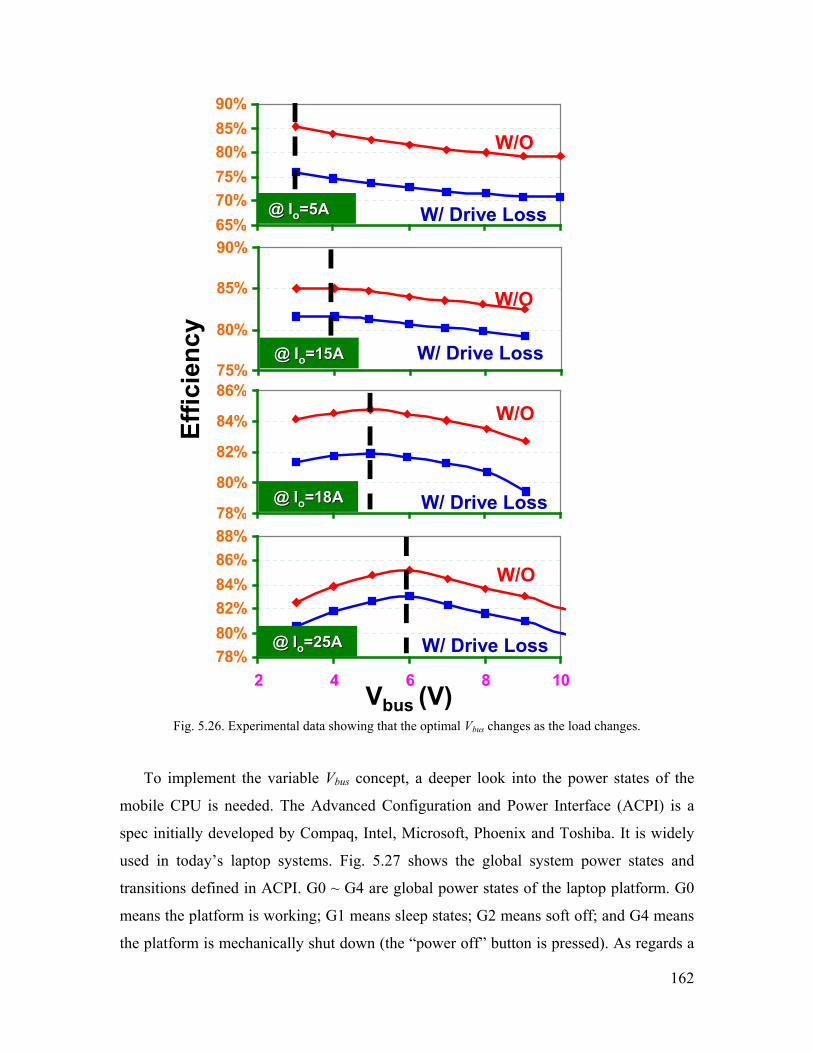
162
65%70%75%80%85%90%
75%
80%
85%
90%
78%
80%
82%
84%
86%
78%80%82%84%86%88%
2 4 6 8 10
W/O
W/ Drive Loss
W/O
W/ Drive Loss
W/O
W/ Drive Loss
W/O
W/ Drive Loss
@ I@ Ioo=18A=18A
@ I@ Ioo=25A=25A
Effic
ienc
y
Vbus (V)
@ I@ Ioo=5A=5A
@ I@ Ioo=15A=15A
Fig. 5.26. Experimental data showing that the optimal Vbus changes as the load changes.
To implement the variable Vbus concept, a deeper look into the power states of the
mobile CPU is needed. The Advanced Configuration and Power Interface (ACPI) is a
spec initially developed by Compaq, Intel, Microsoft, Phoenix and Toshiba. It is widely
used in today’s laptop systems. Fig. 5.27 shows the global system power states and
transitions defined in ACPI. G0 ~ G4 are global power states of the laptop platform. G0
means the platform is working; G1 means sleep states; G2 means soft off; and G4 means
the platform is mechanically shut down (the “power off” button is pressed). As regards a
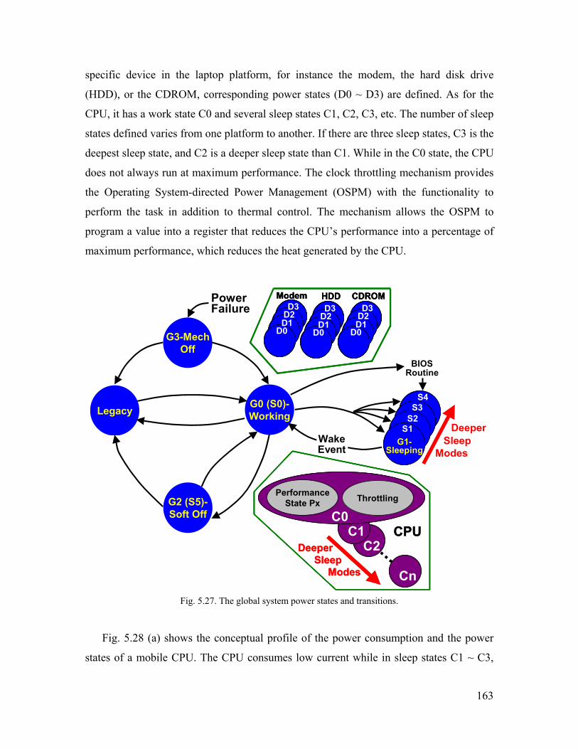
163
specific device in the laptop platform, for instance the modem, the hard disk drive
(HDD), or the CDROM, corresponding power states (D0 ~ D3) are defined. As for the
CPU, it has a work state C0 and several sleep states C1, C2, C3, etc. The number of sleep
states defined varies from one platform to another. If there are three sleep states, C3 is the
deepest sleep state, and C2 is a deeper sleep state than C1. While in the C0 state, the CPU
does not always run at maximum performance. The clock throttling mechanism provides
the Operating System-directed Power Management (OSPM) with the functionality to
perform the task in addition to thermal control. The mechanism allows the OSPM to
program a value into a register that reduces the CPU’s performance into a percentage of
maximum performance, which reduces the heat generated by the CPU.
Legacy
G3-MechOff
G0 (S0)-Working
G2 (S5)-Soft Off
WakeEvent
BIOSRoutine
PowerFailure
DeeperS4
S3S2S2S3
S4
S1G1-
Sleeping
S4S3
S2S2S3
S4
S1G1-
Sleeping
S4S3
S2D1D2D3
D0S4
S3S2D1D2D3
D0S4
S3S2D1D2D3
D0
Modem HDD CDROM
S4S3
S2D1D2D3
D0S4
S3S2D1D2D3
D0S4
S3S2D1D2D3
D0
Modem HDD CDROM
S4S3
S2D1D2D3
D0S4
S3S2D1D2D3
D0S4
S3S2D1D2D3
D0S4
S3S2D1D2D3
D0S4
S3S2D1D2D3
D0S4
S3S2D1D2D3
D0
Modem HDD CDROM
PerformanceState Px Throttling
C0C1
C2
Cn
…CPU
DeeperSleep
Modes
PerformanceState Px Throttling
C0C1
C2
Cn
…CPU
DeeperSleep
Modes
SleepModes
Fig. 5.27. The global system power states and transitions.
Fig. 5.28 (a) shows the conceptual profile of the power consumption and the power
states of a mobile CPU. The CPU consumes low current while in sleep states C1 ~ C3,

164
and performs instructions while in work state C0. During C0, the software dictates the
CPU current; therefore the CPU current is very random in terms of magnitude and
reoccurrence frequency. In the average sense, C0 duration is less than 10~20% of the
total time.
Although the CPU behavior is random during C0, the transition of power states is a
clearly defined event and controlled by the OSPM. For example: C1 is indicated through
the “HLT” pin for IA 32-bit CPUs; C2 is entered by using the “P_LVL2” command
register; and C3 is entered by using the “P_LVL3” command register. The entry/exit of
C1/C2/C3 takes some hardware latency, and the maximum latency is declared in the
Fixed ACPI Description Table (FADT). Upon receiving an interruption, the CPU reads
the required latency value from the FADT and delays for that length before changing its
power state. By doing so the system can make sure that the rest of the platform has been
ready for the new power state when the CPU enters that power state. The latency is in the
100µs plus range.
The CPU is the load for the VR. When the CPU is in C1/C2/C3 states, the current
consumption is a certain value determined by the associated sleep state. When the CPU is
in the C0 state, the current consumption is random from the VR point of view. Based on
this observation, Fig. 5.28 (b) shows the proposed variable Vbus control scheme. When the
CPU is in C1/C2/C3 sleep state, Vbus is positioned at the optimal value associated with the
sleep state; when the CPU is in C0 state, Vbus is positioned at the optimal value associated
with the heavy load, eg: 6V in this case. When there is the CPU power-state transition,
ACPI informs the VR of it and the VR responds by adjusting Vbus. As long as the Vbus
response is quicker than the hardware latency of the state transition, the variable Vbus is
effective in improving the VR efficiency at light load.
Fig. 5.29 shows one implementation of the proposed control scheme. The CPU
power-state information is provided by the ACPI to adjust the reference voltage of the
first-stage buck converter. During the C0 state, Vbus remains constant despite of the load
transitions. For the first-stage converter: the switching frequency is 370KHz, and the
inductance is 2.2µH. The second stage is a three-phase buck converter. The switching
frequency is 1MHz, and the inductance is 150nH. Fig. 5.30 (a) shows the simulation
result of the Vbus transient response. Fig. 5.30 (b) shows the experimental test result. Both

165
tests prove that Vbus response is within 20µs, which is much faster than the hardware
latency for CPU power-state transition. The first-stage switching at 370KHz is the main
reason why Vbus response is so quick.
Software-related load transient
Time
CPUPower C0 C0 C0
C1 C2 C3 C1C2C3 C1 C2 C3 C1C2C3
Deeper Sleep State
(a)
Time
Vbus
6V 6V 6V
< 6V < 6V
(b)
Fig. 5.28. The proposed adjustable Vbus: (a) The Mobile CPU Power States and the Power Consumption,
and (b) the proposed variable Vbus control scheme based on the ACPI information.
CbusVin Q12Q11
CoQ2Q1
Q4Q3
Q6Q5
L1
L2
L3
Loadi
EA
L11
VoVbus
refV
Sleep Mode Work ModeC1/C2/C3... C0
CPU Power State Info(Through the ACPI)
Fig. 5.29. The implementation of the variable Vbus control scheme based on the ACPI information.
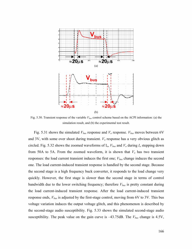
166
Vbus
≈20µs ≈20µs (a)
≈20µs ≈20µs
Vbus
(b)
Fig. 5.30. Transient response of the variable Vbus control scheme based on the ACPI information: (a) the
simulation result, and (b) the experimental test result.
Fig. 5.31 shows the simulated Vbus response and Vo response. Vbus moves between 6V
and 3V, with some over shoot during transient. Vo response has a very obvious glitch as
circled. Fig. 5.32 shows the zoomed waveforms of Io, Vbus and Vo during Io stepping down
from 50A to 5A. From the zoomed waveform, it is shown that Vo has two transient
responses: the load current transient induces the first one; Vbus change induces the second
one. The load current-induced transient response is handled by the second stage. Because
the second stage is a high frequency buck converter, it responds to the load change very
quickly. However, the first stage is slower than the second stage in terms of control
bandwidth due to the lower switching frequency; therefore Vbus is pretty constant during
the load current-induced transient response. After the load current-induced transient
response ends, Vbus is adjusted by the first-stage control, moving from 6V to 3V. This bus
voltage variation induces the output voltage glitch, and this phenomenon is described by
the second-stage audio susceptibility. Fig. 5.33 shows the simulated second-stage audio
susceptibility. The peak value on the gain curve is –43.75dB. The Vbus change is 4.5V,

167
considering the overshoot. (4.5 V)×(–43.75 dB)=30 mV, and 30 mV is just the magnitude
of the glitch on Vo waveform.
Vbus
(a)
Vo
(b)
Fig. 5.31. Simulated Vbus response and Vo response: (a) Vbus response with 3V change in magnitude, and
(b) Vo response showing an obvious glitch.
Io
Io-Induced Transient Response
Vbus–Induced Transient Response
(Appears first)
(Appears second)
Vo
Vbus
Fig. 5.32. Zoomed-in waveforms of Io step change, Vbus response and Vo response.

168
f(Hz)100 1K 10K 100K 1M
Gai
n (d
B) 60
40
Phas
e (°
) 0
100
100
-
-
-
100
80
-
-
120-
200-
Fig. 5.33. The simulated audio susceptibility of the second stage.
One way to reduce the Vo glitch is to further attenuate the audio susceptibility. The
method for accomplishing this is to further increase the second-stage bandwidth.
However, this requires higher switching frequency of the second stage, which decreases
the efficiency.
Another way is to add a feed forward function into the second-stage converter, as
shown in Fig. 5.34. Vpp is the ramp amplitude of the second-stage buck converter. The
feed forward function controls Vpp such that it is proportional to Vbus, that is
ppbus VkV ×= (5.2)
where k is a constant. The duty cycle is
pp
c
VV
D = (5.3)
Therefore
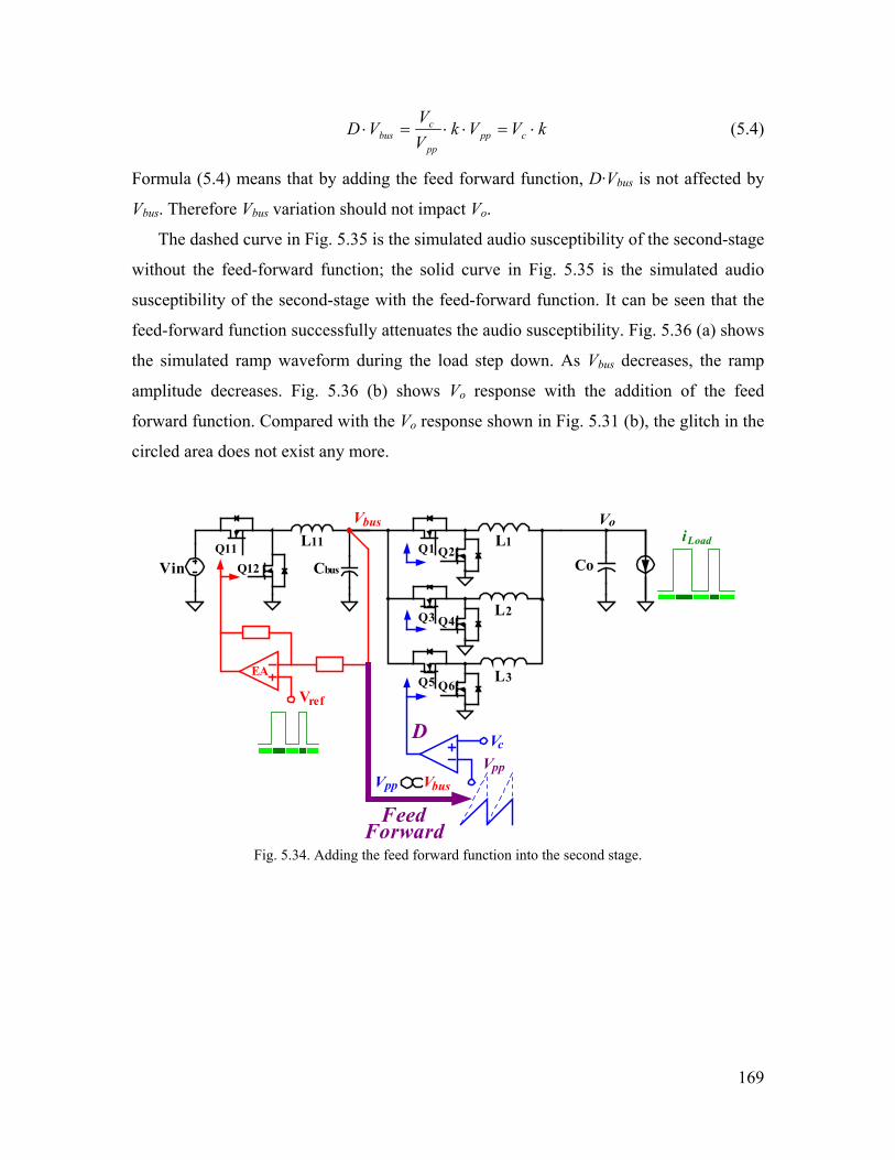
169
kVVkVV
VD cpppp
cbus ⋅=⋅⋅=⋅ (5.4)
Formula (5.4) means that by adding the feed forward function, D·Vbus is not affected by
Vbus. Therefore Vbus variation should not impact Vo.
The dashed curve in Fig. 5.35 is the simulated audio susceptibility of the second-stage
without the feed-forward function; the solid curve in Fig. 5.35 is the simulated audio
susceptibility of the second-stage with the feed-forward function. It can be seen that the
feed-forward function successfully attenuates the audio susceptibility. Fig. 5.36 (a) shows
the simulated ramp waveform during the load step down. As Vbus decreases, the ramp
amplitude decreases. Fig. 5.36 (b) shows Vo response with the addition of the feed
forward function. Compared with the Vo response shown in Fig. 5.31 (b), the glitch in the
circled area does not exist any more.
CbusVin Q12Q11
CoQ2Q1
Q4Q3
Q6Q5
L1
L2
L3EA
L11
VoVbus
refV
ppV Vbus
cV
FeedForward
D
Loadi
ppV
Fig. 5.34. Adding the feed forward function into the second stage.
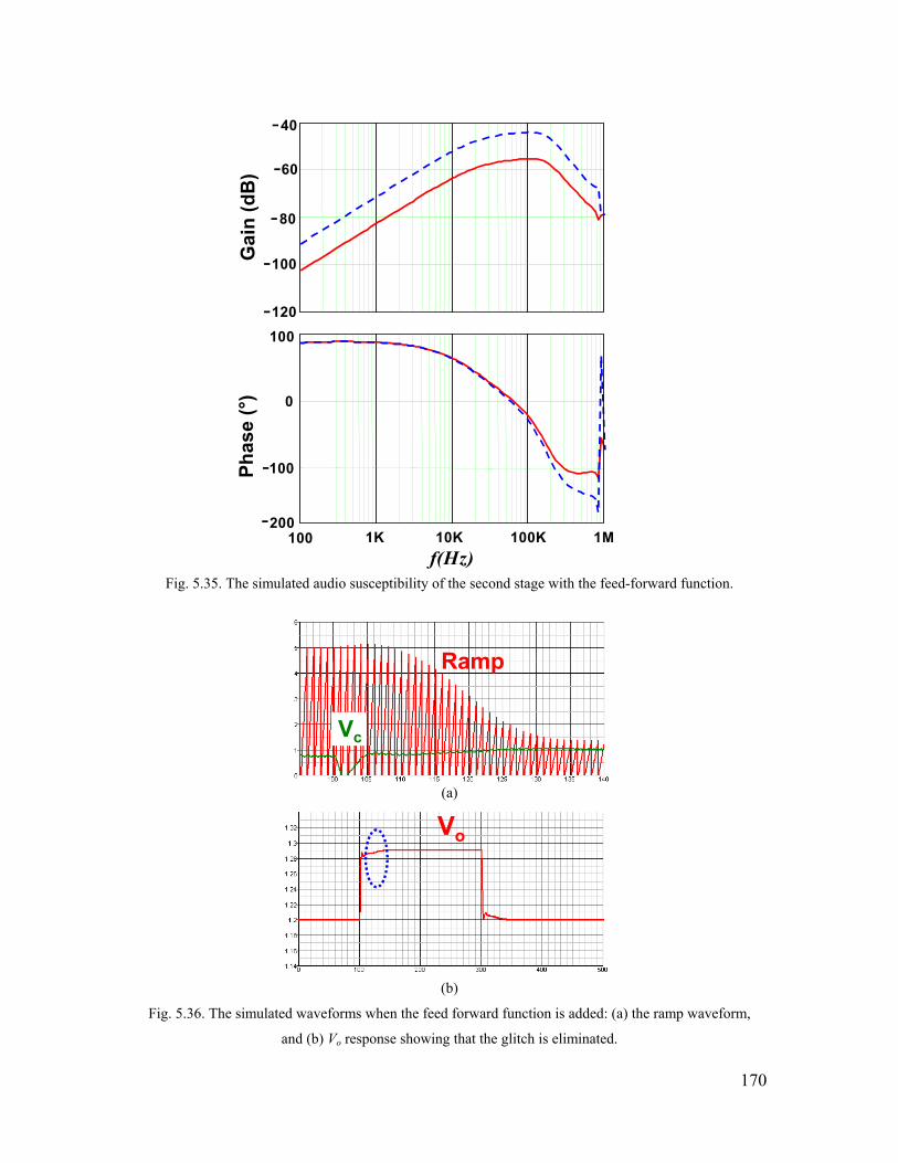
170
f(Hz)100 1K 10K 100K 1M
Gai
n (d
B) 60
40
Phas
e (°
) 0
100
100
-
-
-
100
80
-
-
120-
200-
Fig. 5.35. The simulated audio susceptibility of the second stage with the feed-forward function.
Ramp
Vc
(a)
Vo
(b)
Fig. 5.36. The simulated waveforms when the feed forward function is added: (a) the ramp waveform,
and (b) Vo response showing that the glitch is eliminated.

171
5.5. Improving Light-Load Efficiency Through the Proposed Adaptive Bus-
Voltage Positioning (ABVP).
The ACPI-based variable Vbus control scheme can guarantee that Vbus is optimal
during the sleep states. However, during the C0 state, Vbus is not always optimal. Fig.
5.37 shows that when the CPU is in C0 state, the CPU could be drawing maximum
current, but also could draw lower current. Since the ACPI-based Vbus control scheme
sets Vbus at 6V during the entire C0 state, Vbus is not optimal when the CPU is not drawing
maximum current, marked as the shaded area in Fig. 5.37. Depending on users and
software, the CPU could be in C0 state for most of the time. So there is a pretty good
chance that the shaded areas become dominant. In this case, the bus voltage not being
optimal is significantly bad for efficiency.
Fig. 5.38 shows the ideal positioning of Vbus. The ideal Vbus should be positioned
according to the load current at any time, therefore optimal efficiency can be achieved at
any load. The optimal Vbus trend shown in Fig. 5.26 can be drawn in Fig. 5.39 (a) as the
solid line. It is not a direct line. When the load decreases from full load, the optimal Vbus
decreases. In 45~25A range, the slope of the optimal Vbus-Io line is not very steep; in the
25~3A range, the slope of the optimal Vbus-Io line is steeper. When Vbus reaches 3V at 3A
output, because less than 3V is too low to be practical, it is not further decreased when
the load is less than 3A. The dashed line in Fig. 5.39 (a) is one method to approximate the
solid line. Vbus is kept at 6 V in 45~25A range, decreases linearly to 3V in 25~3A range,
and maintains 3V in 3~0A range. Fig. 5.39 (b) shows another method to approximate the
solid line. Vbus decreases linearly from 6 V to 3 V in the 45A ~ 0A range. The method is
shown in Fig. 5.39 (b) is less accurate, but simpler. Both methods incorporate the element
of Vbus decreasing linearly according to Io. This becomes the key in the implementation.
The adaptive voltage positioning (AVP) concept is already widely used today at the
VR output Vo. AVP positions Vbus according to the load current, described as the load
line. The slope of the load line is defined as Rdroop. Fig. 5.40 shows the proposed adaptive
bus-voltage positioning (ABVP) concept. The ABVP concept also positions Vbus
according to the load current. Different from AVP is that ABVP increases Vbus when Io
increases, as opposed to AVP decreasing Vo when Io increases. The slope of the Vbus-Io
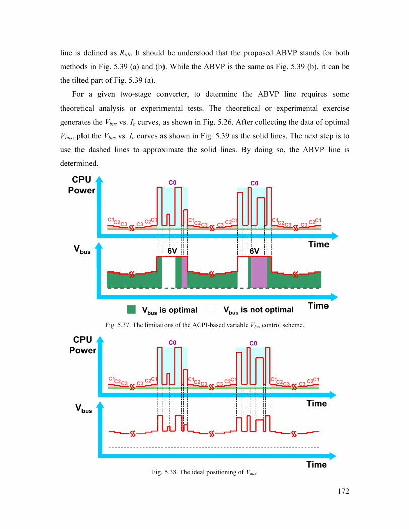
172
line is defined as Rtilt. It should be understood that the proposed ABVP stands for both
methods in Fig. 5.39 (a) and (b). While the ABVP is the same as Fig. 5.39 (b), it can be
the tilted part of Fig. 5.39 (a).
For a given two-stage converter, to determine the ABVP line requires some
theoretical analysis or experimental tests. The theoretical or experimental exercise
generates the Vbus vs. Io curves, as shown in Fig. 5.26. After collecting the data of optimal
Vbus, plot the Vbus vs. Io curves as shown in Fig. 5.39 as the solid lines. The next step is to
use the dashed lines to approximate the solid lines. By doing so, the ABVP line is
determined.
Time
CPUPower
C0 C0
Time
Vbus
C1C2C3C1C2C3
C1C2C3C1C2C3
C1C2C3C1C2C3
6V6V6V6V
Vbus is optimal Vbus is not optimal
Fig. 5.37. The limitations of the ACPI-based variable Vbus control scheme.
Time
CPUPower
C0 C0
C1C2C3C1C2C3
C1C2C3C1C2C3
C1C2C3C1C2C3
Time
Vbus
Fig. 5.38. The ideal positioning of Vbus.
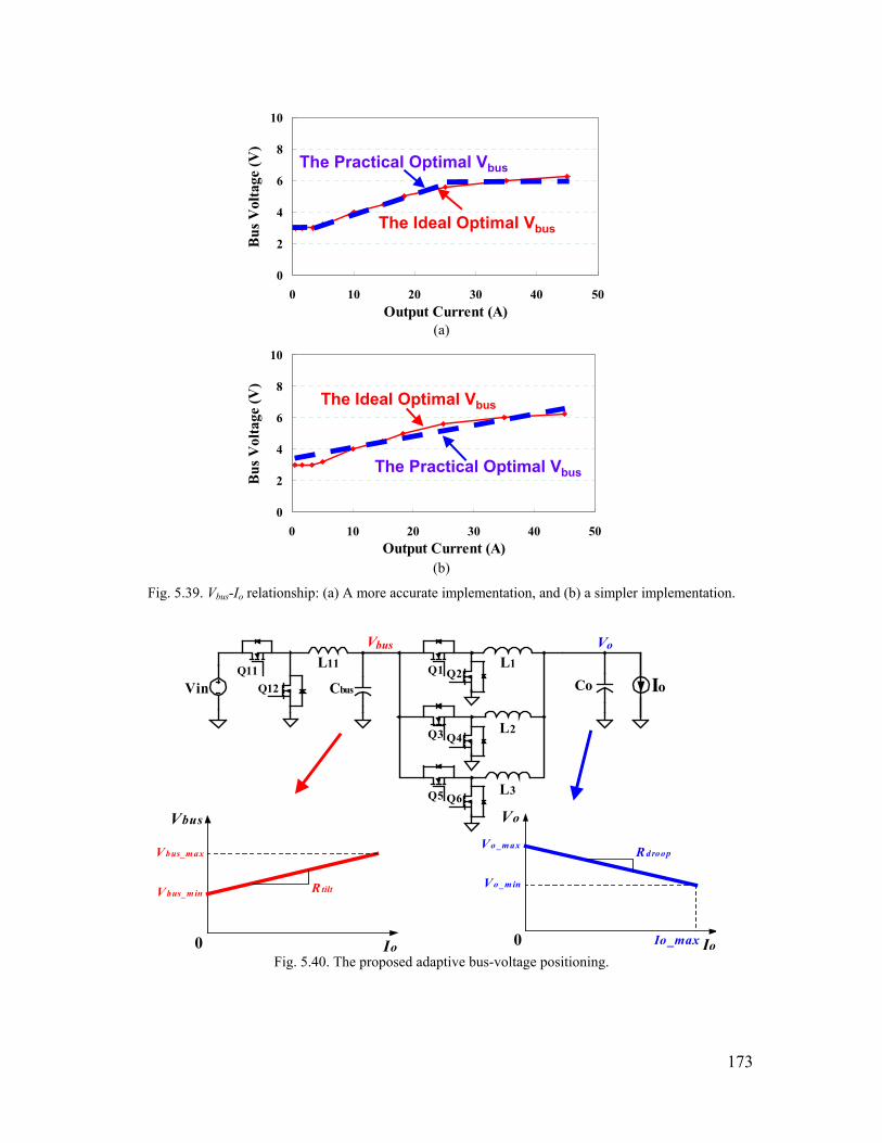
173
0
2
4
6
8
10
0 10 20 30 40 50Output Current (A)
Bus
Vol
tage
(V)
The Ideal Optimal Vbus
The Practical Optimal Vbus
(a)
0
2
4
6
8
10
0 10 20 30 40 50Output Current (A)
Bus
Vol
tage
(V)
The Ideal Optimal Vbus
The Practical Optimal Vbus
(b)
Fig. 5.39. Vbus-Io relationship: (a) A more accurate implementation, and (b) a simpler implementation.
Io
Vo
Vo_m ax
Vo_m in
Io_max0
Rdroop
Io
Vbus
Vbus_m ax
V bus_m in Rtilt
0
CbusVin Q12Q11
CoQ2Q1
Q4Q3
Q6Q5
L1
L2
L3
L11
VoVbus
Io
Fig. 5.40. The proposed adaptive bus-voltage positioning.
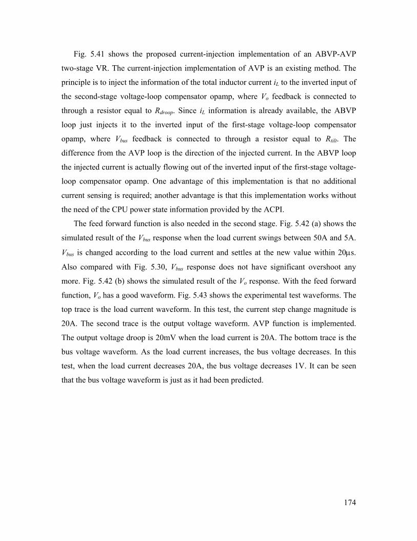
174
Fig. 5.41 shows the proposed current-injection implementation of an ABVP-AVP
two-stage VR. The current-injection implementation of AVP is an existing method. The
principle is to inject the information of the total inductor current iL to the inverted input of
the second-stage voltage-loop compensator opamp, where Vo feedback is connected to
through a resistor equal to Rdroop. Since iL information is already available, the ABVP
loop just injects it to the inverted input of the first-stage voltage-loop compensator
opamp, where Vbus feedback is connected to through a resistor equal to Rtilt. The
difference from the AVP loop is the direction of the injected current. In the ABVP loop
the injected current is actually flowing out of the inverted input of the first-stage voltage-
loop compensator opamp. One advantage of this implementation is that no additional
current sensing is required; another advantage is that this implementation works without
the need of the CPU power state information provided by the ACPI.
The feed forward function is also needed in the second stage. Fig. 5.42 (a) shows the
simulated result of the Vbus response when the load current swings between 50A and 5A.
Vbus is changed according to the load current and settles at the new value within 20µs.
Also compared with Fig. 5.30, Vbus response does not have significant overshoot any
more. Fig. 5.42 (b) shows the simulated result of the Vo response. With the feed forward
function, Vo has a good waveform. Fig. 5.43 shows the experimental test waveforms. The
top trace is the load current waveform. In this test, the current step change magnitude is
20A. The second trace is the output voltage waveform. AVP function is implemented.
The output voltage droop is 20mV when the load current is 20A. The bottom trace is the
bus voltage waveform. As the load current increases, the bus voltage decreases. In this
test, when the load current decreases 20A, the bus voltage decreases 1V. It can be seen
that the bus voltage waveform is just as it had been predicted.

175
CbusVin Q12Q11
CoQ2Q1
Q4Q3
Q6Q5
L1
L2
L3EA
Vref
L11VoVbus
EAVID
iL
iL
Rdroop
Rtilt
ppV Vbus
cV
Feed Forward
ppV
LoadiiLiL1iL11
Fig. 5.41. The proposed current-injection implementation of ABVP.
Vbus
≈20µs ≈20µs
(a)
Vo
(b)
Fig. 5.42. Simulation result of the proposed current-injection implementation of ABVP: (a) Vbus response
and (b) Vo response.
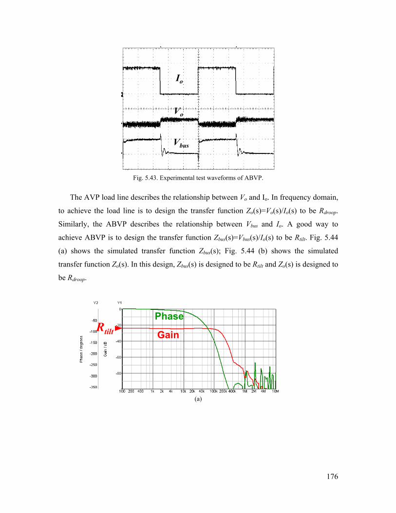
176
Vbus
Vo
Io
Fig. 5.43. Experimental test waveforms of ABVP.
The AVP load line describes the relationship between Vo and Io. In frequency domain,
to achieve the load line is to design the transfer function Zo(s)=Vo(s)/Io(s) to be Rdroop.
Similarly, the ABVP describes the relationship between Vbus and Io. A good way to
achieve ABVP is to design the transfer function Zbus(s)=Vbus(s)/Io(s) to be Rtilt. Fig. 5.44
(a) shows the simulated transfer function Zbus(s); Fig. 5.44 (b) shows the simulated
transfer function Zo(s). In this design, Zbus(s) is designed to be Rtilt and Zo(s) is designed to
be Rdroop.
Gain
PhaseRtilt
(a)
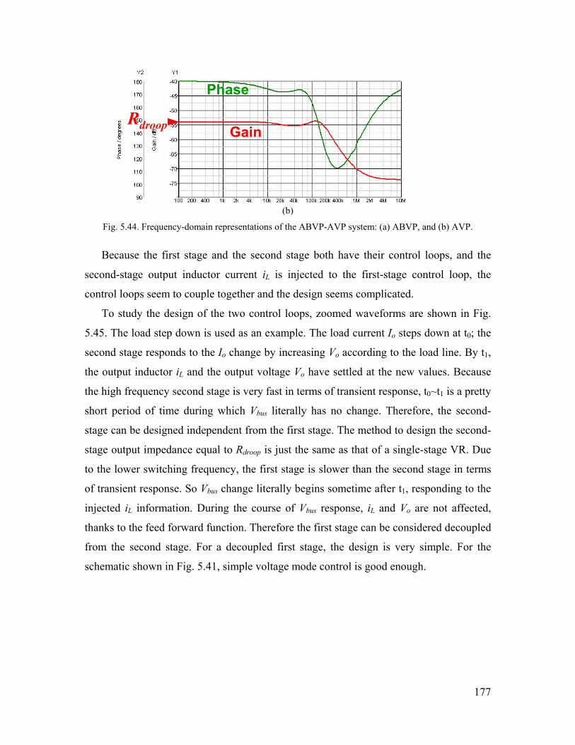
177
Gain
Phase
Rdroop
(b)
Fig. 5.44. Frequency-domain representations of the ABVP-AVP system: (a) ABVP, and (b) AVP.
Because the first stage and the second stage both have their control loops, and the
second-stage output inductor current iL is injected to the first-stage control loop, the
control loops seem to couple together and the design seems complicated.
To study the design of the two control loops, zoomed waveforms are shown in Fig.
5.45. The load step down is used as an example. The load current Io steps down at t0; the
second stage responds to the Io change by increasing Vo according to the load line. By t1,
the output inductor iL and the output voltage Vo have settled at the new values. Because
the high frequency second stage is very fast in terms of transient response, t0~t1 is a pretty
short period of time during which Vbus literally has no change. Therefore, the second-
stage can be designed independent from the first stage. The method to design the second-
stage output impedance equal to Rdroop is just the same as that of a single-stage VR. Due
to the lower switching frequency, the first stage is slower than the second stage in terms
of transient response. So Vbus change literally begins sometime after t1, responding to the
injected iL information. During the course of Vbus response, iL and Vo are not affected,
thanks to the feed forward function. Therefore the first stage can be considered decoupled
from the second stage. For a decoupled first stage, the design is very simple. For the
schematic shown in Fig. 5.41, simple voltage mode control is good enough.

178
Io
Vo
Vbus
iL
t0 t1 Fig. 5.45. The zoomed waveforms of the current-injection ABVP-AVP two-stage VR.

179
The ABVP control intends to position Vbus according to Io at any time. However,
when the CPU is in C0 state, software can create Io transients with all possible amplitudes
and reoccurrence frequencies up to several MHz. How the ABVP-AVP VR responds to
various Io transients is an interesting aspect to examine. For further study, two parameters
are defined: fc1 is the control bandwidth of the first stage; fc2 is the control bandwidth of
the second stage. For a meaningful two-stage VR, the second stage switches at a higher
frequency than the first stage; therefore there is fc1< fc2.
When the Io transient reoccurrence frequency fIo is lower than fc1, there is fIo< fc1< fc2.
Then the first and the second stages are both fast enough to catch up with the Io transient.
Fig. 5.46 shows the simulation waveforms. Io transients have random amplitudes, but the
reoccurrence frequencies are low. IL1 is one phase inductor current of the second stage. iL1
is 1/3 of the instantaneous Io with the addition of some switching ripple. At any Io, Vbus is
set at the value determined by the Vbus-Io line shown in Fig. 5.40. Vbus is always optimal
in this scenario. Vo is set at the value determined by the load line shown in Fig. 5.40.
Io
Software-related load transient
Sleep State
iL1

180
Vbus
Vo
Fig. 5.46. The ABVP-AVP response when there is fIo< fc1< fc2.
When the Io transient reoccurrence frequency fIo is higher than fc2, there is fc1< fc2< fIo.
Then the Io transient is too fast to respond to for both the first and the second stages. Fig.
5.47 (a) shows the simulation waveforms. Io swings between 50A and 5A at 5MHz
reoccurrence frequency. Fig. 5.47 (b) shows iL1 waveform, which is one phase inductor
current of the second stage. Due to the limited second-stage control bandwidth fc2 (<5
MHz), iL1 does not respond to the 5MHz Io transient. As the result, iL1 is 1/3 of the
average value of Io with the addition of some switching ripple. Fig. 5.47 (c) shows iL11
waveform, which is the inductor current of the first stage. Because the second stage only
sees a load of average Io, and the second stage is the load for the first stage, iL11 is also the
result of the load of average Io. Therefore the optimal Vbus is determined by the average
value of Io in this scenario, and that’s exactly what the ABVP control does. Fig. 5.48
shows the simulation transient response of the ABVP-AVP system. Compared with Fig.
5.46, Io has an additional 5 MHZ transient during ta~tb. Therefore Vbus is set at the value
determined by the Vbus-Io line shown in Fig. 5.40, according to the average value of Io.
Vbus is always optimal in this scenario. Vo is set at the value determined by the load line
shown in Fig. 5.40, according to the average value of Io.

181
Io 5MHz
(a)
iL1
(b)
iL11
(c)
Fig. 5.47. The inductor current waveforms when there is fc1< fc2< fIo: (a) Io, (b) iL1, and (c) iL11.

182
Io
5MHz Transients
ta tb
iL1
ABVP
Vbus
Vo
Fig. 5.48. The ABVP-AVP response when there is fc1< fc2< fIo.

183
When the Io transient reoccurrence frequency fIo is between fc1 and fc2, there is fc1< fIo
<fc2. Then the second stage is able to respond to Io transient, while the first stage cannot.
In the two-stage design that been used in this chapter, the first-stage switching frequency
is 370KHz and the control bandwidth is fc1=60KHz; second-stage switching frequency is
1MHz and the control bandwidth is fc2=160KHz. As shown in Fig. 5.49 (a), Io swings
between 50A and 5A at 100KHz reoccurrence frequency. Fig. 5.49 (b) shows iL1
waveform. iL1 is able to respond to the 100KHz Io transient. As a result, iL1 is 1/3 of the
instantaneous value of Io with the addition of some switching ripple. Fig. 5.49 (c) shows
iL11 waveform. Although the second stage sees the instantaneous Io, the first stage is not
fast enough to respond to the 100KHz transient power drawn by the second stage. So iL11
is still the result of the load of average Io. Because the first and the second stages see Io in
two different ways, there is not an optimal Vbus defined for this scenario. Fig. 5.49 (d)
shows the Vbus waveform. It can be seen that the first stage tries to adjust Vbus according
to the instantaneous value of Io, but cannot quite do it due to the limited fc1. Vbus then has
a 100KHz ripple on top of the DC value determined by the average Io. Fig. 5.49 (e) shows
the Vo waveform. Vo is set at the value determined by the load line shown in Fig. 5.40,
according to the instantaneous value of Io.
As a summary, the ABVP control can guarantee the optimal Vbus when the CPU is in
sleep states. When the CPU is in work state, the ABVP control guarantees optimal Vbus if
the load transient reoccurrence frequency is lower than fc1 or higher than fc2; optimal Vbus
cannot be guaranteed when the load transient reoccurrence frequency is between fc1 and
fc2. The difference between fc1 and fc2 is due to the different switching frequencies of the
two stages.
Io 100KHz
(a)

184
iL1
(b)
iL11
(c)
Vbus
(d)
Vo
(e)
Fig. 5.49. The inductor current waveforms when fc1 < fIo< fc2: (a) Io, (b) iL1, (c) iL11, (b) Vbus, and (e) Vo.
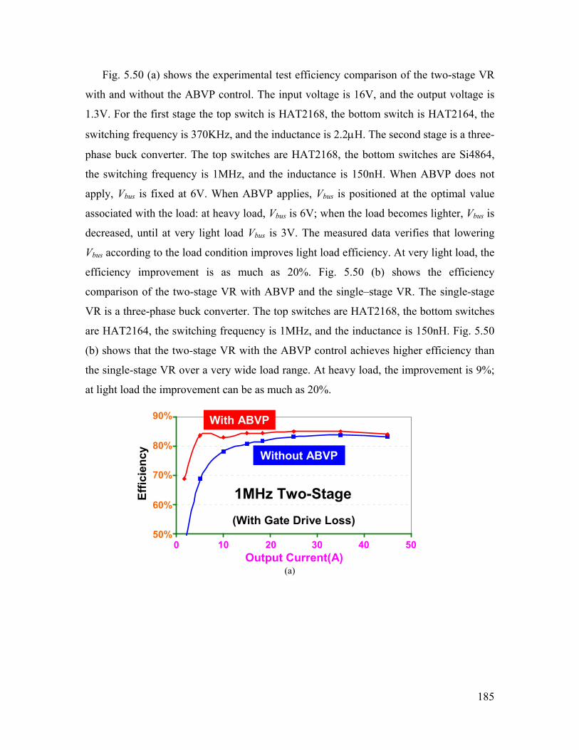
185
Fig. 5.50 (a) shows the experimental test efficiency comparison of the two-stage VR
with and without the ABVP control. The input voltage is 16V, and the output voltage is
1.3V. For the first stage the top switch is HAT2168, the bottom switch is HAT2164, the
switching frequency is 370KHz, and the inductance is 2.2µH. The second stage is a three-
phase buck converter. The top switches are HAT2168, the bottom switches are Si4864,
the switching frequency is 1MHz, and the inductance is 150nH. When ABVP does not
apply, Vbus is fixed at 6V. When ABVP applies, Vbus is positioned at the optimal value
associated with the load: at heavy load, Vbus is 6V; when the load becomes lighter, Vbus is
decreased, until at very light load Vbus is 3V. The measured data verifies that lowering
Vbus according to the load condition improves light load efficiency. At very light load, the
efficiency improvement is as much as 20%. Fig. 5.50 (b) shows the efficiency
comparison of the two-stage VR with ABVP and the single–stage VR. The single-stage
VR is a three-phase buck converter. The top switches are HAT2168, the bottom switches
are HAT2164, the switching frequency is 1MHz, and the inductance is 150nH. Fig. 5.50
(b) shows that the two-stage VR with the ABVP control achieves higher efficiency than
the single-stage VR over a very wide load range. At heavy load, the improvement is 9%;
at light load the improvement can be as much as 20%.
10 20 30 40 50Output Current(A)
50%
60%
70%
80%
90%
0
Effic
ienc
y
(With Gate Drive Loss)
With ABVP
Without ABVP
1MHz Two-Stage
(a)
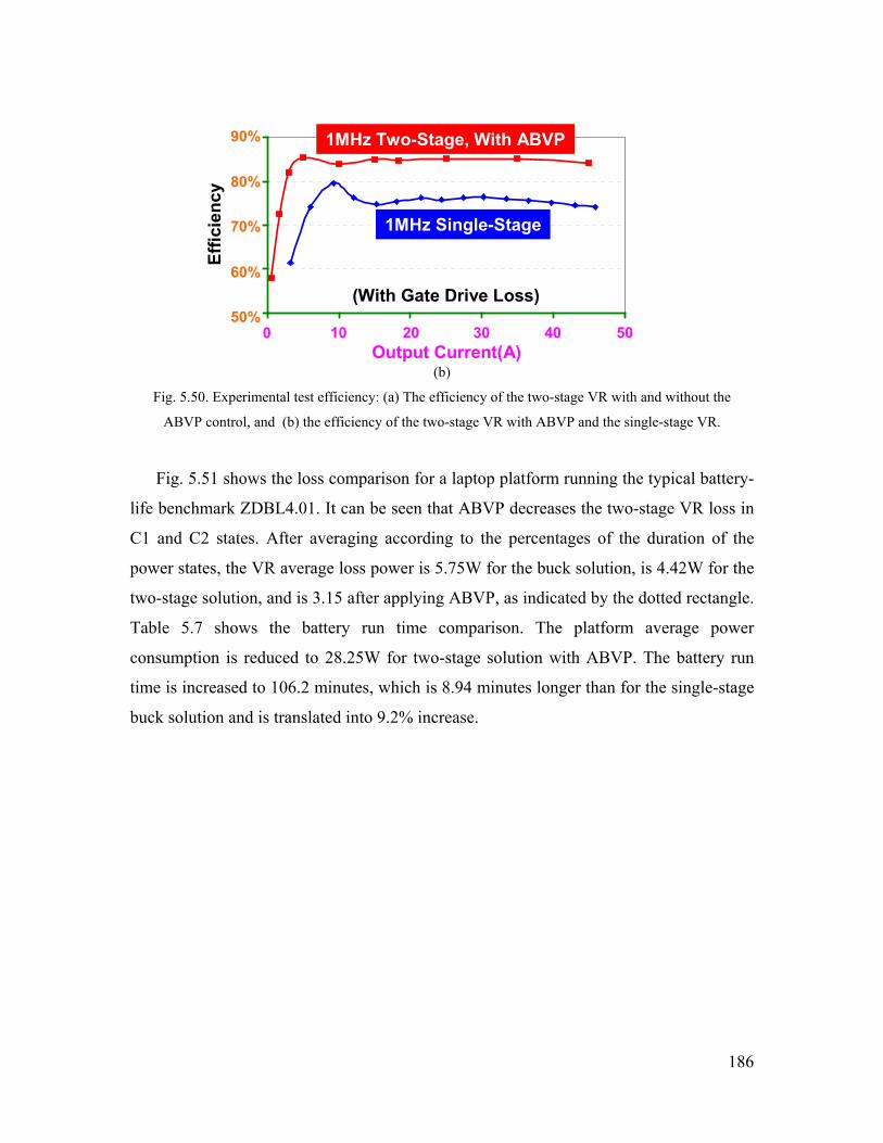
186
10 20 30 40 50Output Current(A)
50%
60%
70%
80%
90%
0
Effic
ienc
y
(With Gate Drive Loss)
1MHz Two-Stage, With ABVP
1MHz Single-Stage
(b)
Fig. 5.50. Experimental test efficiency: (a) The efficiency of the two-stage VR with and without the
ABVP control, and (b) the efficiency of the two-stage VR with ABVP and the single-stage VR.
Fig. 5.51 shows the loss comparison for a laptop platform running the typical battery-
life benchmark ZDBL4.01. It can be seen that ABVP decreases the two-stage VR loss in
C1 and C2 states. After averaging according to the percentages of the duration of the
power states, the VR average loss power is 5.75W for the buck solution, is 4.42W for the
two-stage solution, and is 3.15 after applying ABVP, as indicated by the dotted rectangle.
Table 5.7 shows the battery run time comparison. The platform average power
consumption is reduced to 28.25W for two-stage solution with ABVP. The battery run
time is increased to 106.2 minutes, which is 8.94 minutes longer than for the single-stage
buck solution and is translated into 9.2% increase.
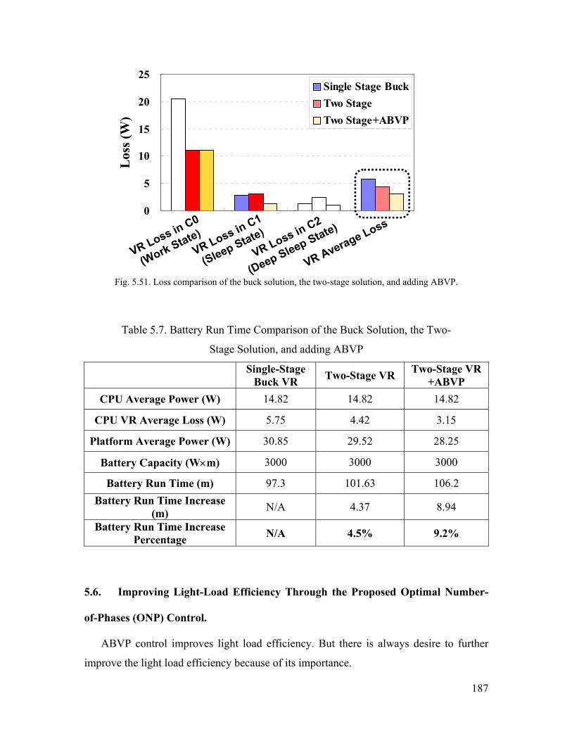
187
0
5
10
15
20
25
Los
s (W
)
Single Stage BuckTwo StageTwo Stage+ABVP
VR Loss in C0
(Work State)VR Loss in C1
(Sleep State)
VR Loss in C2
(Deep Sleep State)
VR Average Loss
Fig. 5.51. Loss comparison of the buck solution, the two-stage solution, and adding ABVP.
Table 5.7. Battery Run Time Comparison of the Buck Solution, the Two-
Stage Solution, and adding ABVP
Single-Stage Buck VR Two-Stage VR Two-Stage VR
+ABVP CPU Average Power (W) 14.82 14.82 14.82
CPU VR Average Loss (W) 5.75 4.42 3.15
Platform Average Power (W) 30.85 29.52 28.25
Battery Capacity (W×m) 3000 3000 3000
Battery Run Time (m) 97.3 101.63 106.2 Battery Run Time Increase
(m) N/A 4.37 8.94
Battery Run Time Increase Percentage N/A 4.5% 9.2%
5.6. Improving Light-Load Efficiency Through the Proposed Optimal Number-
of-Phases (ONP) Control.
ABVP control improves light load efficiency. But there is always desire to further
improve the light load efficiency because of its importance.

188
Fig. 5.52 (a) shows one phase of the second-stage multiphase buck converter. The
devices have parasitic drain-source capacitors Coss1 and Coss2. At light load, because the
average output current iL1 is very low, the conduction loss is no longer a big contributor
in the total loss, while several losses become more significant.
Fig. 5.52 (b) shows the gate-source voltages of the switches. The gate drive loss is
sqggategate fQQVP ⋅+⋅= )( 21 (5.5)
where Vgate is the gate drive voltage; Qg1 and Qg2 are the gate charges of Q1 and Q2; and
fs is the switching frequency.
Fig. 5.52 (c) shows the inductor current iL1 waveform. Although the average of iL1 is
very low, the current ripple still exists and Q1 is turned off at a higher current. The turn-
off loss of Q1 is
sstressoffg
qsgdpkLoffturn fv
iQQ
iP ⋅⋅+
⋅=− _1
2_1 (5.6)
where iL1_pk is the peak value of iL1; Qgd and Qgs2 are two gate charge parameters of Q1;
voff_stress is the turn-off voltage stress of Q1; and fs is the switching frequency.
Fig. 5.52 (d) shows the phase voltage vphase1 waveform. When Q1 is on, Coss2 is
charged to Vbus. This charge process is lossy. When Q1 is off, the inductor current iL1
discharges Coss2 and make the body-diode of Q2 conduct. This discharge process is
lossless. Therefore the loss caused by the charging-discharging of Coss2 is
sbusosss fVCP ⋅⋅⋅= 222cos 3
2 (5.7)
Also there is the body-diode reverse recovery loss, given by formula (5.8)
sbusrrrr fVQP ⋅⋅= (5.8)
The losses given by formulas (5.5) ~ (5.8) are all present even when the load current
is very low. They are the main reasons why the buck converter suffers low efficiency at
light load. Moreover, since Pgate, Pturn-off, Pcoss2 and Prr are all proportional to the
switching frequency fs, they become more significant when the VR is switching at MHz.
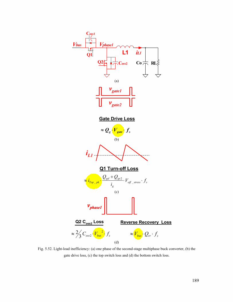
189
Co RLQ2Q1 L1
Vphase1
Coss2
Coss1
Vbus
iL1
(a)
sgateg fVQ ⋅⋅≈
Gate Drive Loss
vgate1
vgate2
(b)
iL1
sstressoffg
gsgdpkTop fV
iQQ
i ⋅⋅+
⋅≈ _2
_
Q1 Turn-off Loss
(c)
vphase1vphase1
Reverse Recovery LossQ2 Coss2 Loss
sbusoss fVC ⋅⋅≈ 223
2srrbus fQV ⋅⋅≈
(d)
Fig. 5.52. Light-load inefficiency: (a) one phase of the second-stage multiphase buck converter, (b) the
gate drive loss, (c) the top switch loss and (d) the bottom switch loss.
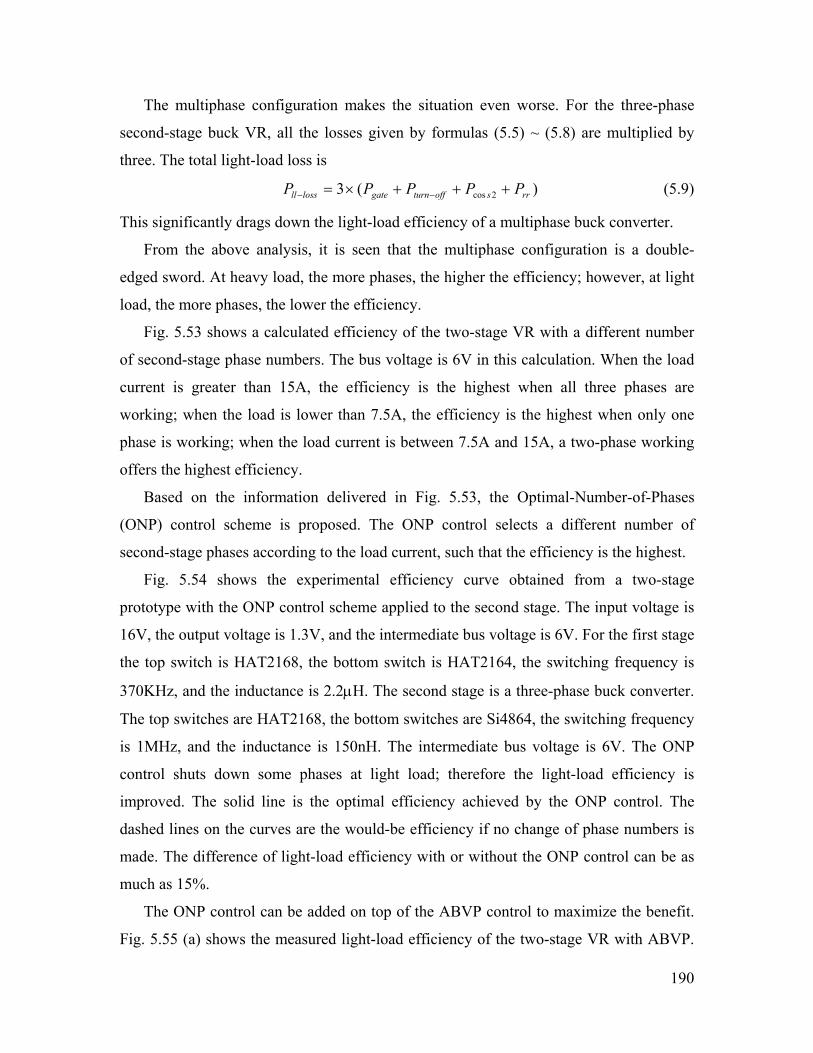
190
The multiphase configuration makes the situation even worse. For the three-phase
second-stage buck VR, all the losses given by formulas (5.5) ~ (5.8) are multiplied by
three. The total light-load loss is
)(3 2cos rrsoffturngatelossll PPPPP +++×= −− (5.9)
This significantly drags down the light-load efficiency of a multiphase buck converter.
From the above analysis, it is seen that the multiphase configuration is a double-
edged sword. At heavy load, the more phases, the higher the efficiency; however, at light
load, the more phases, the lower the efficiency.
Fig. 5.53 shows a calculated efficiency of the two-stage VR with a different number
of second-stage phase numbers. The bus voltage is 6V in this calculation. When the load
current is greater than 15A, the efficiency is the highest when all three phases are
working; when the load is lower than 7.5A, the efficiency is the highest when only one
phase is working; when the load current is between 7.5A and 15A, a two-phase working
offers the highest efficiency.
Based on the information delivered in Fig. 5.53, the Optimal-Number-of-Phases
(ONP) control scheme is proposed. The ONP control selects a different number of
second-stage phases according to the load current, such that the efficiency is the highest.
Fig. 5.54 shows the experimental efficiency curve obtained from a two-stage
prototype with the ONP control scheme applied to the second stage. The input voltage is
16V, the output voltage is 1.3V, and the intermediate bus voltage is 6V. For the first stage
the top switch is HAT2168, the bottom switch is HAT2164, the switching frequency is
370KHz, and the inductance is 2.2µH. The second stage is a three-phase buck converter.
The top switches are HAT2168, the bottom switches are Si4864, the switching frequency
is 1MHz, and the inductance is 150nH. The intermediate bus voltage is 6V. The ONP
control shuts down some phases at light load; therefore the light-load efficiency is
improved. The solid line is the optimal efficiency achieved by the ONP control. The
dashed lines on the curves are the would-be efficiency if no change of phase numbers is
made. The difference of light-load efficiency with or without the ONP control can be as
much as 15%.
The ONP control can be added on top of the ABVP control to maximize the benefit.
Fig. 5.55 (a) shows the measured light-load efficiency of the two-stage VR with ABVP.

191
For the upper curve, the ONP control kicks in when the load is less than 5A; for the lower
curve, all the phases are switching even at light load. It is seen that the efficiency is
increased by 10% after the ONP control is applied.
Fig. 5.55 (b) shows the efficiency comparison of the two-stage VR and the single–
stage VR. The two-stage VR features ABVP and ONP controls. It is shown that the two-
stage VR has much higher efficiency than the single-stage VR over a wide load range
(100:1 in this test).
65%
70%
75%
80%
85%
90%
0 5 10 15 20 25 30Output Current (A)
Effic
ienc
y
3φ Working
1φ Working1φ Working
2φ Working2φ Working
Fig. 5.53. Calculated efficiency with different numbers of 2nd-stage phases.
Output Current(A)
50%
60%
70%
80%
90%
0 10 20 30 40 50
Effic
ienc
y
Output Current(A)
Co RLQ2Q1 L1
Co RLQ2Q1
Q4Q3
L1
L2
C o RLQ 2Q 1
Q 4Q 3
Q 6Q 5
L1
L2
L3
Including Gate Drive LossIncluding Gate Drive Loss
Fig. 5.54. Experimental verification of efficiency improvement of the ONP control.
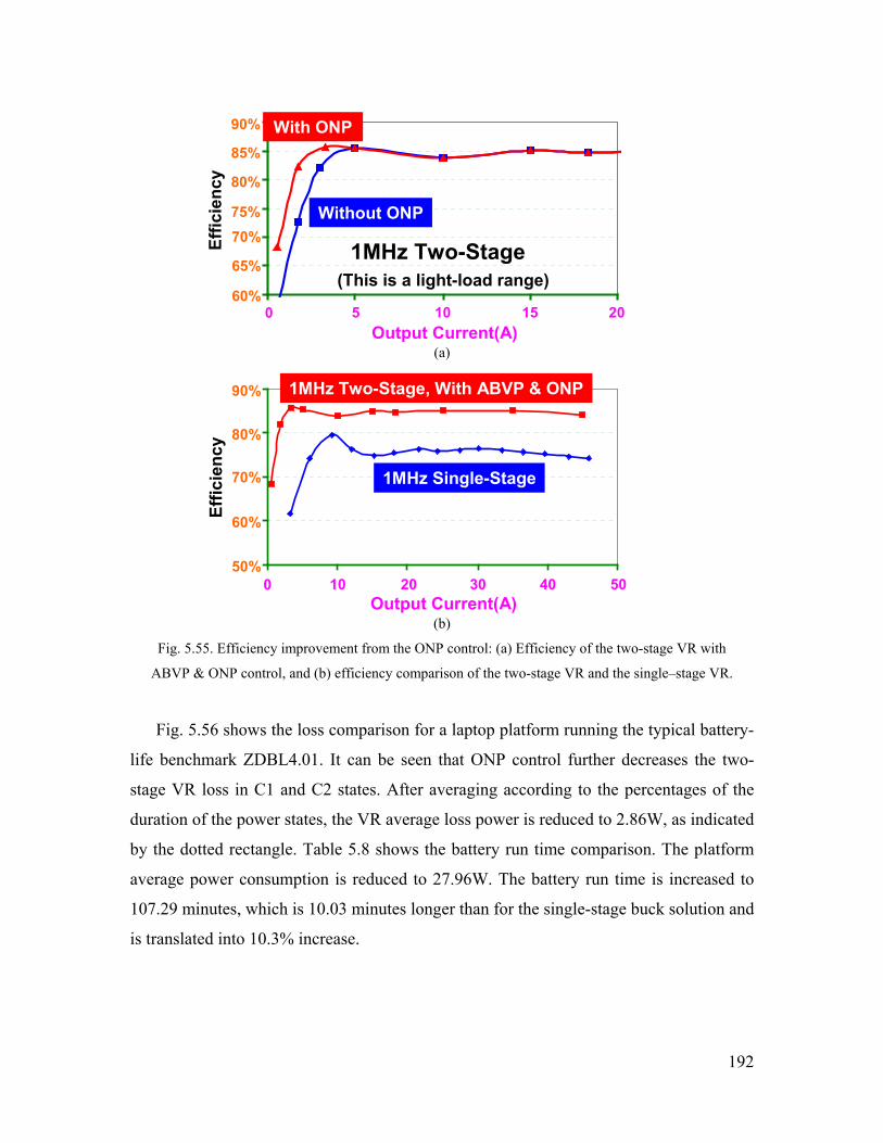
192
5 10 15 20Output Current(A)
0
75%
80%
85%
90%
Effic
ienc
y
60%
65%
70%Without ONP
With ONP
(This is a light-load range)1MHz Two-Stage
(a)
50%
60%
70%
80%
90%
Effic
ienc
y
10 20 30 40 50Output Current(A)
0
1MHz Single-Stage
1MHz Two-Stage, With ABVP & ONP
(b)
Fig. 5.55. Efficiency improvement from the ONP control: (a) Efficiency of the two-stage VR with
ABVP & ONP control, and (b) efficiency comparison of the two-stage VR and the single–stage VR.
Fig. 5.56 shows the loss comparison for a laptop platform running the typical battery-
life benchmark ZDBL4.01. It can be seen that ONP control further decreases the two-
stage VR loss in C1 and C2 states. After averaging according to the percentages of the
duration of the power states, the VR average loss power is reduced to 2.86W, as indicated
by the dotted rectangle. Table 5.8 shows the battery run time comparison. The platform
average power consumption is reduced to 27.96W. The battery run time is increased to
107.29 minutes, which is 10.03 minutes longer than for the single-stage buck solution and
is translated into 10.3% increase.
193
0
5
10
15
20
25
Los
s (W
)Single Stage BuckTwo StageTwo Stage+ABVPTwo Stage+ABVP+ONP
VR Loss in C0
(Work State)VR Loss in C1
(Sleep State)
VR Loss in C2
(Deep Sleep State)
VR Average Loss
Fig. 5.56. Loss comparison of the buck solution, the two-stage solution, adding ABVP, and adding ONP.
Table 5.8. Battery Run Time Comparison of the Buck Solution, the Two-
Stage Solution, adding ABVP and adding ONP
Single-Stage
Buck VR
Two-Stage VR
Two-Stage VR +ABVP
Two-Stage VR +ABVP+ONP
CPU Average Power (W) 14.82 14.82 14.82 14.82
CPU VR Average Loss (W) 5.75 4.42 3.15 2.86
Platform Average Power (W) 30.85 29.52 28.25 27.96
Battery Capacity (W×m) 3000 3000 3000 3000
Battery Run Time (m) 97.3 101.63 106.2 107.29
Battery Run Time Increase (m) N/A 4.37 8.94 10.03
Battery Run Time Increase
Percentage N/A 4.5% 9.2% 10.3%
It should be brought to attention that turning on or turning off a phase should be an
ACPI event, not a response to the software-related light load. The VR controller receives
194
the ACPI signal and therefore knows what power state the processor is in and will be in.
Then the VR selects the optimum number of phases associated with the power state. For
example: Use three phases at C0 state, use two phases at C1 state, and use one phase at
C2 state. By doing so, the VR has high efficiency when the processor is in sleep states.
5.7. Improving Very-Light-Load Efficiency Through the Proposed Baby-Buck
(BB) Concept.
With ABVP and ONP controls, the two-stage VR has greatly improved efficiency
compared with the single-stage VR, as is shown in Fig. 5.55 (b). However, the very light-
load efficiency still leaves room for further improvement.
At very light load, the second-stage is already a single-phase buck converter working
with low Vbus. However, this single-phase buck converter is optimized for heavy load
operation, namely 15~20A per phase. Therefore the devices have fairly large current-
handling capability, hence fairly large gate charge, drain-source capacitance and reverse-
recovery charge. As discussed in section 6.6, these large parameters tend to drag down
the efficiency at light load.
If a buck converter is optimized for light load, it can be very efficient. Fig. 5.57
shows the efficiency curve from TPS54612 monolithic buck converter. The switching
frequency is 350KHz, and the efficiency reaches 95% when the load current is less than
3A.
Fig. 5.58 shows the proposed baby-buck concept. The second stage has an additional
buck channel called baby buck. The baby-buck channel is a tiny buck converter
optimized at a very low current level, e.g.: less than 3A. It can even be a monolithically
integrated power IC. The control scheme of the baby buck can be combined with the
ONP control. When the load decreases, the main phases are shut down one by one, until
when Io is less than 3A, all the main phases are down, leaving only the baby buck channel
working. By doing so, the very light load efficiency can be high. However, since the baby
buck is not designed to carry high current, it must have current-limiting function. When
the load is heavy, the baby buck is still handling 3A, and the rest of the load current is
handled and shared by the main phases.

195
Fig. 5.59 (a) shows the efficiency comparison of the two-stage VR featuring ABVP
and ONP controls. For the upper curve at very-light-load range, only the baby buck
channel is working; for the lower curve, there is no baby-buck channel, so a “strong”
phase is working. It can be seen that the baby buck concept can greatly improve the very-
light-load efficiency. Fig. 5.59 (b) shows the efficiency comparison between the single-
stage VR and the two-stage VR featuring ABVP, ONP and baby buck concepts. The
input voltage is 16V, and the output voltage is 1.3V. The single-stage VR is a three-phase
buck converter. The top switches are HAT2168, the bottom switches are HAT2164, the
switching frequency is 1MHz, and the inductance is 150nH. In the two-stage VR, for the
first stage the top switch is HAT2168, the bottom switch is HAT2164, the switching
frequency is 370KHz, and the inductance is 2.2µH; the second stage is a three-phase
buck converter. The top switches are HAT2168, the bottom switches are Si4864, the
switching frequency is 1MHz, and the inductance is 150nH. The lower curve is the
single-stage VR efficiency. The upper curve is the efficiency of the two-stage VR
featuring ABVP, ONP and baby buck. This comparison shows that the two-stage
architecture with the advanced control concepts is much more efficient than the single-
stage architecture within a wide load range (100:1 in this test).
Source: TPS54612 Datasheet
Fig. 5.57. Efficiency of TPS54612 monolithic buck converter.

196
C busVin Q12Q11
Co RLQ2Q1
Q4Q3
Q6Q5
L
L
L
Q8Q7 L'Baby-Buck Channel
Fig. 5.58. The proposed baby-buck concept.
5 10 15 20Output Current(A)
0
75%
80%
85%
90%
Effic
ienc
y
60%
65%
70%
Without BB
With BB
(This is a light-load range)1MHz Two-Stage
(a)
10 20 30 40Output Current(A)
0 50
1MHz Two-Stage, With ABVP, ONP & BB
1MHz Single-Stage
50%
60%
70%
80%
90%
Effic
ienc
y
(b)
Fig. 5.59. Efficiency of the two-stage VR: (a) The two-stage VR efficiency with and without the baby-
buck concept; and (b) the efficiency comparison between the single stage VR and the two-stage VR
featuring ABVP, ONP and BB concepts.
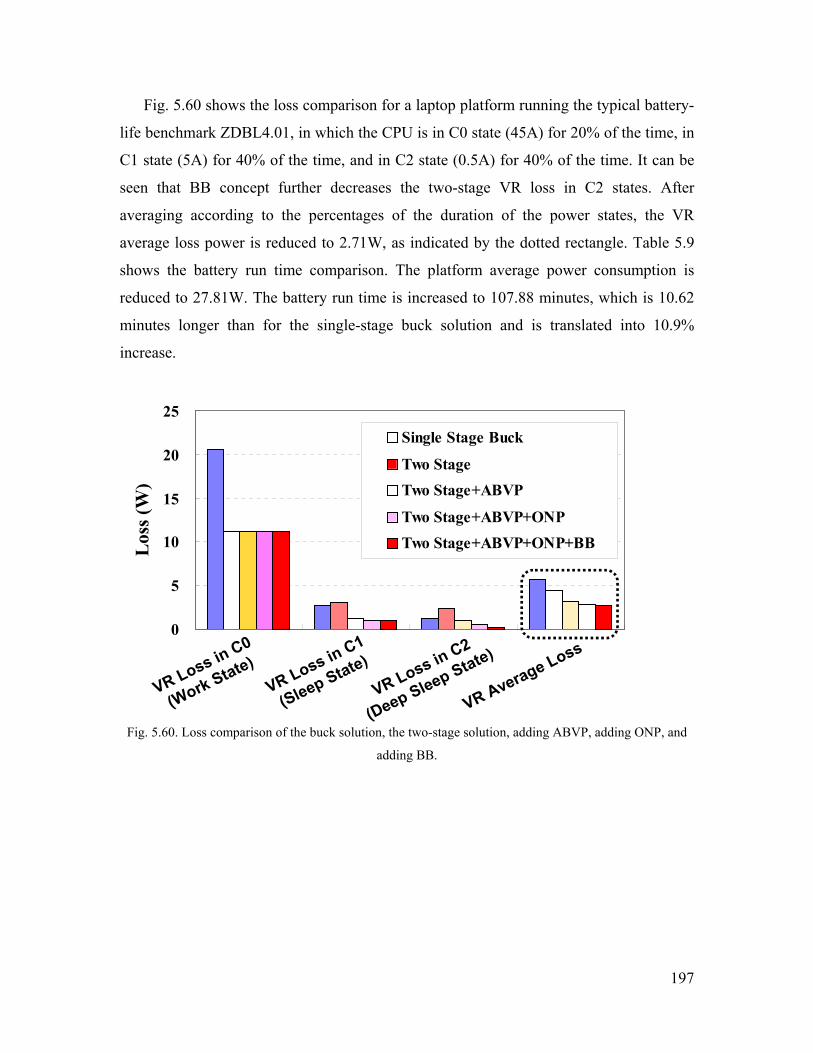
197
Fig. 5.60 shows the loss comparison for a laptop platform running the typical battery-
life benchmark ZDBL4.01, in which the CPU is in C0 state (45A) for 20% of the time, in
C1 state (5A) for 40% of the time, and in C2 state (0.5A) for 40% of the time. It can be
seen that BB concept further decreases the two-stage VR loss in C2 states. After
averaging according to the percentages of the duration of the power states, the VR
average loss power is reduced to 2.71W, as indicated by the dotted rectangle. Table 5.9
shows the battery run time comparison. The platform average power consumption is
reduced to 27.81W. The battery run time is increased to 107.88 minutes, which is 10.62
minutes longer than for the single-stage buck solution and is translated into 10.9%
increase.
0
5
10
15
20
25
Los
s (W
)
Single Stage Buck
Two StageTwo Stage+ABVP
Two Stage+ABVP+ONPTwo Stage+ABVP+ONP+BB
VR Loss in C0
(Work State)VR Loss in C1
(Sleep State)
VR Loss in C2
(Deep Sleep State)
VR Average Loss
Fig. 5.60. Loss comparison of the buck solution, the two-stage solution, adding ABVP, adding ONP, and
adding BB.
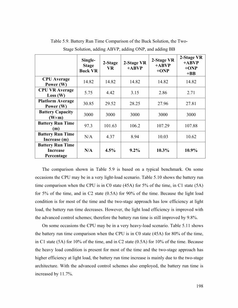
198
Table 5.9. Battery Run Time Comparison of the Buck Solution, the Two-
Stage Solution, adding ABVP, adding ONP, and adding BB
Single-Stage
Buck VR
2-Stage VR
2-Stage VR +ABVP
2-Stage VR +ABVP +ONP
2-Stage VR +ABVP +ONP +BB
CPU Average Power (W) 14.82 14.82 14.82 14.82 14.82
CPU VR Average Loss (W) 5.75 4.42 3.15 2.86 2.71
Platform Average Power (W) 30.85 29.52 28.25 27.96 27.81
Battery Capacity (W×m) 3000 3000 3000 3000 3000
Battery Run Time (m) 97.3 101.63 106.2 107.29 107.88
Battery Run Time Increase (m) N/A 4.37 8.94 10.03 10.62
Battery Run Time Increase
Percentage N/A 4.5% 9.2% 10.3% 10.9%
The comparison shown in Table 5.9 is based on a typical benchmark. On some
occasions the CPU may be in a very light-load scenario. Table 5.10 shows the battery run
time comparison when the CPU is in C0 state (45A) for 5% of the time, in C1 state (5A)
for 5% of the time, and in C2 state (0.5A) for 90% of the time. Because the light load
condition is for most of the time and the two-stage approach has low efficiency at light
load, the battery run time decreases. However, the light load efficiency is improved with
the advanced control schemes; therefore the battery run time is still improved by 9.8%.
On some occasions the CPU may be in a very heavy-load scenario. Table 5.11 shows
the battery run time comparison when the CPU is in C0 state (45A) for 80% of the time,
in C1 state (5A) for 10% of the time, and in C2 state (0.5A) for 10% of the time. Because
the heavy load condition is present for most of the time and the two-stage approach has
higher efficiency at light load, the battery run time increase is mainly due to the two-stage
architecture. With the advanced control schemes also employed, the battery run time is
increased by 11.7%.

199
Table 5.10. Battery Run Time Comparison at Extremely Light Load
Single-Stage
Buck VR
2-Stage VR
2-Stage VR +ABVP
2-Stage VR +ABVP +ONP
2-Stage VR +ABVP +ONP +BB
CPU Average Power (W) 4.42 4.42 14.82 14.82 14.82
CPU VR Average Loss (W) 2.34 2.88 1.58 1.16 0.81
Platform Average Power (W) 17.04 17.58 16.28 15.86 15.51
Battery Capacity (W×m) 3000 3000 3000 3000 3000
Battery Run Time (m) 176.09 170.62 184.32 189.20 193.40
Battery Run Time Increase (m) N/A -5.47 8.23 13.11 17.31
Battery Run Time Increase
Percentage N/A -3.1% 4.7% 7.4% 9.8%
Table 5.11. Battery Run Time Comparison at Extremely Heavy Load
Single-Stage
Buck VR
2-Stage VR
2-Stage VR +ABVP
2-Stage VR +ABVP +ONP
2-Stage VR +ABVP +ONP +BB
CPU Average Power (W) 47.58 47.58 47.58 47.58 47.58
CPU VR Average Loss (W) 16.85 9.46 9.14 9.07 9.03
Platform Average Power (W) 74.71 67.32 67.00 66.93 66.89
Battery Capacity (W×m) 3000 3000 3000 3000 3000
Battery Run Time (m) 40.15 44.56 44.77 44.82 44.85
Battery Run Time Increase (m) N/A 4.41 4.62 4.67 4.69
Battery Run Time Increase
Percentage N/A 11.0% 11.5% 11.6% 11.7%
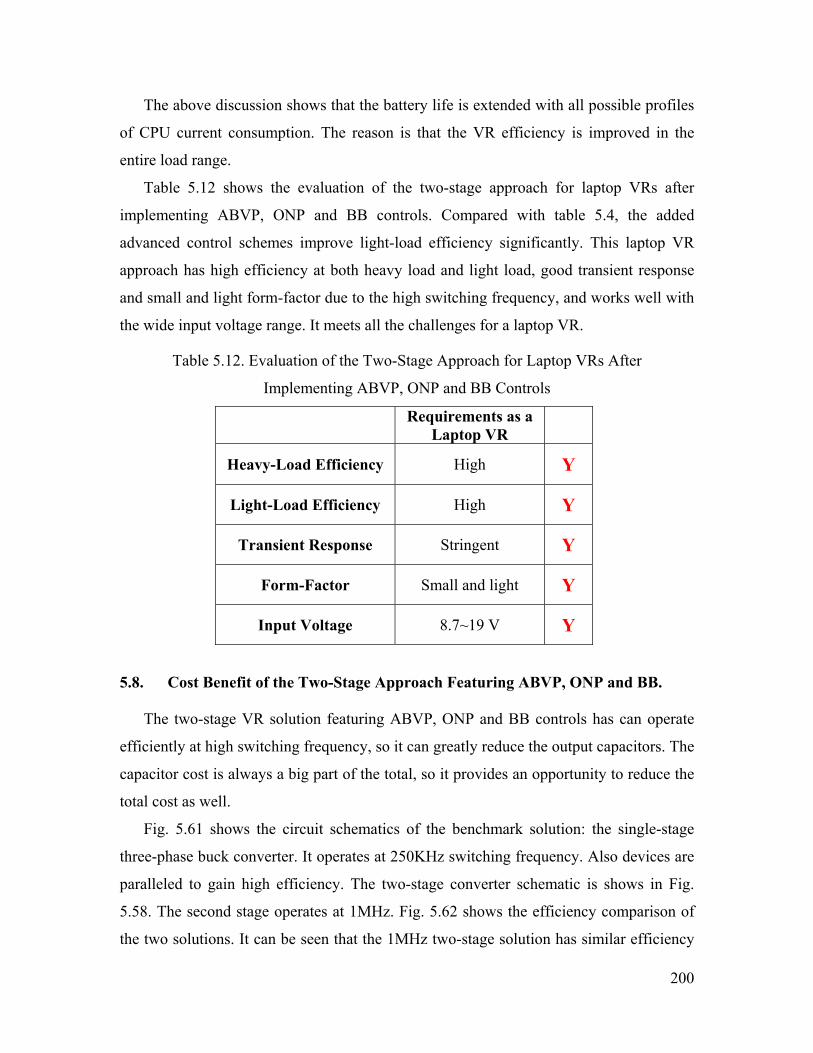
200
The above discussion shows that the battery life is extended with all possible profiles
of CPU current consumption. The reason is that the VR efficiency is improved in the
entire load range.
Table 5.12 shows the evaluation of the two-stage approach for laptop VRs after
implementing ABVP, ONP and BB controls. Compared with table 5.4, the added
advanced control schemes improve light-load efficiency significantly. This laptop VR
approach has high efficiency at both heavy load and light load, good transient response
and small and light form-factor due to the high switching frequency, and works well with
the wide input voltage range. It meets all the challenges for a laptop VR.
Table 5.12. Evaluation of the Two-Stage Approach for Laptop VRs After
Implementing ABVP, ONP and BB Controls
Requirements as a Laptop VR
Heavy-Load Efficiency High Y
Light-Load Efficiency High Y
Transient Response Stringent Y
Form-Factor Small and light Y
Input Voltage 8.7~19 V Y
5.8. Cost Benefit of the Two-Stage Approach Featuring ABVP, ONP and BB.
The two-stage VR solution featuring ABVP, ONP and BB controls has can operate
efficiently at high switching frequency, so it can greatly reduce the output capacitors. The
capacitor cost is always a big part of the total, so it provides an opportunity to reduce the
total cost as well.
Fig. 5.61 shows the circuit schematics of the benchmark solution: the single-stage
three-phase buck converter. It operates at 250KHz switching frequency. Also devices are
paralleled to gain high efficiency. The two-stage converter schematic is shows in Fig.
5.58. The second stage operates at 1MHz. Fig. 5.62 shows the efficiency comparison of
the two solutions. It can be seen that the 1MHz two-stage solution has similar efficiency
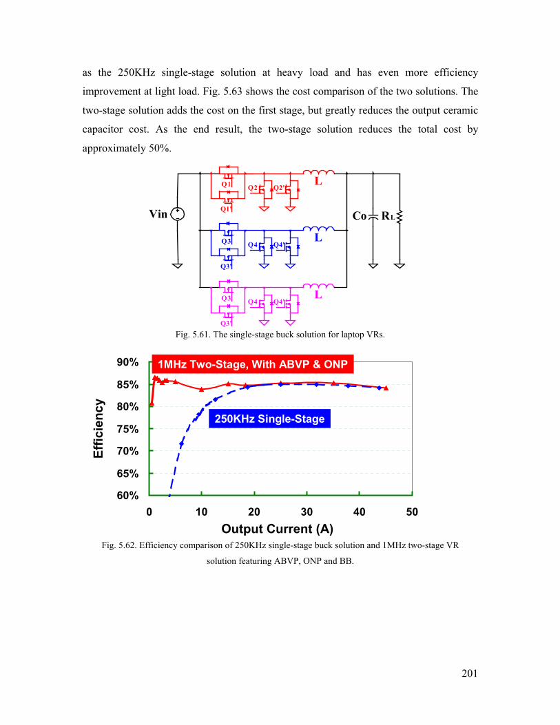
201
as the 250KHz single-stage solution at heavy load and has even more efficiency
improvement at light load. Fig. 5.63 shows the cost comparison of the two solutions. The
two-stage solution adds the cost on the first stage, but greatly reduces the output ceramic
capacitor cost. As the end result, the two-stage solution reduces the total cost by
approximately 50%.
Co RLVin
Q2'Q1
Q3 Q4'
L
L
Q2
Q4
Q3'
Q1'
Q3 Q4'L
Q4
Q3' Fig. 5.61. The single-stage buck solution for laptop VRs.
60%
65%
70%
75%
80%
85%
90%
0 10 20 30 40 50Output Current (A)
Effic
ienc
y
250KHz Single-Stage
1MHz Two-Stage, With ABVP & ONP
Fig. 5.62. Efficiency comparison of 250KHz single-stage buck solution and 1MHz two-stage VR
solution featuring ABVP, ONP and BB.
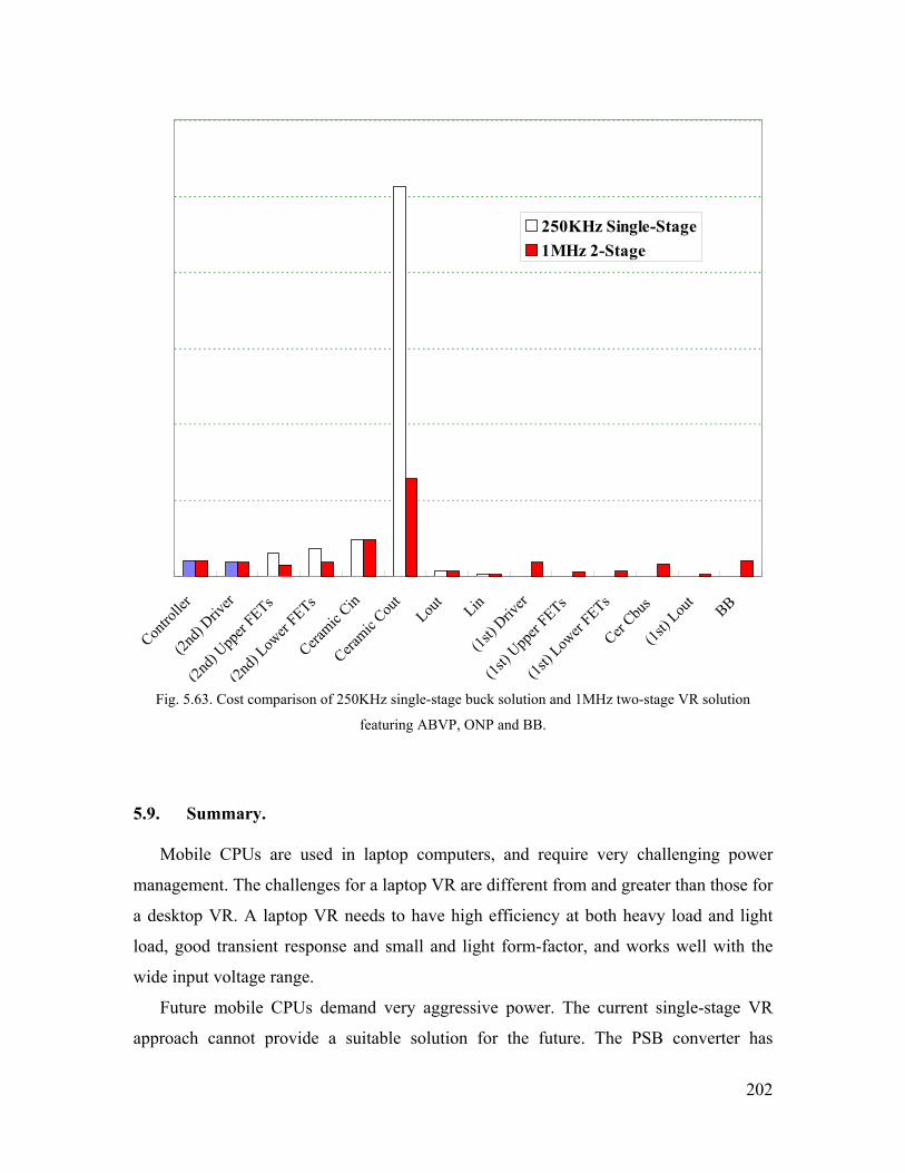
202
Contro
ller
(2nd)
Driver
(2nd)
Upper
FETs
(2nd)
Lower
FETs
Ceramic
Cin
Ceramic
Cout
Lout
Lin
(1st) D
river
(1st) U
pper
FETs
(1st) L
ower
FETs
Cer Cbu
s
(1st) L
out
BB
250KHz Single-Stage1MHz 2-Stage
Fig. 5.63. Cost comparison of 250KHz single-stage buck solution and 1MHz two-stage VR solution
featuring ABVP, ONP and BB.
5.9. Summary.
Mobile CPUs are used in laptop computers, and require very challenging power
management. The challenges for a laptop VR are different from and greater than those for
a desktop VR. A laptop VR needs to have high efficiency at both heavy load and light
load, good transient response and small and light form-factor, and works well with the
wide input voltage range.
Future mobile CPUs demand very aggressive power. The current single-stage VR
approach cannot provide a suitable solution for the future. The PSB converter has

203
disadvantages in light-load efficiency and does not work well with wide input voltage
range; therefore it is not a suitable solution for laptop VRs even although it is still a
suitable solution for desktop VRs. The two-stage approach has been explored in desktop
VR application and is proven to be a good solution. The laptop VR is a better fit for the
two-stage approach. It solves the wide-input-voltage-range issue and significantly
improves efficiency at heavy load.
The intermediate bus voltage Vbus is a very important parameter impacting overall
efficiency. There is not one optimal Vbus value for all load conditions. The heavier the
load, the higher the optimal Vbus is. Based on this fact, the ABVP control is proposed. Vbus
is adaptively positioned according to the load current; therefore optimal Vbus is achieved
under most conditions. Experimental results verify this theoretical prediction.
The ONP control is another control scheme proposed to improve light-load
efficiency. By selecting optimal number of phases based on mobile processor power
states, the VR light-load efficiency is improved. Experimental results verify this.
The baby-buck concept is the third concept proposed to improve the very-light-load
efficiency. By operating the baby-buck channel, the two-stage VR improves efficiency at
very light load.
The two-stage VR featuring the three proposed control schemes has much higher
efficiency than the single-stage VR over a very wide load range; therefore the battery life
is extended.
204
Chapter 6. Conclusion
VR is a dedicated DC-DC converter to power the microprocessor. It faces great
challenges in terms of keeping pace with the fast development of microprocessors. The
state-of-the-art VR solution is the multiphase buck converter. Historically the VR works
with 5V input and delivers 2V or so output voltage at 10, 20A output current. However,
the new generations of microprocessors demand even lower core voltage with tighter
regulation, while drawing substantially higher current. To reduce the distribution loss, the
VR input voltage increases to 12V. After the VR input voltage changes from 5V to 12V,
coupled with the fact that the output voltage goes down to less than 1V with high current,
the VR suffers both low efficiency and bad transient response. When the buck VR works
with 12V input and sub 1V output, the duty cycle is very small. The extreme duty cycle
increases VR switching loss, reverse recovery loss, and conduction loss; therefore makes
the 12V-input VR efficiency drop a good deal when compared with 5V-input VR
efficiency. It has an emergent need to improve VR efficiency. When the VR works with
5V input voltage, it always has symmetrical transient response. When the input voltage
increases to 12V, because of the extreme duty cycle, load step up and load step down
suggest a candidate for the critical inductance respectively. The smaller one should be the
critical inductance. If the real inductance is smaller than the critical inductance, the
transient response is symmetrical; if the real inductance is larger than the critical
inductance, the transient response is asymmetric and has larger voltage spike. The current
VR practice is a trade-off between efficiency and transient response. The choice of the
inductance is larger than the critical inductance in order to achieve high efficiency. The
result is bad transient response.
The bad transient response of current VR solution is handled by using many
capacitors. Future microprocessors will demand higher current with lower voltage and
tighter regulation. If VR design follows the current approach, the future VR solution will
be very bulky and costly. Adaptive voltage positioning (AVP) is a requirement for VR.
The essence is to try to make the VR output impedance equal to the load line slope Rdroop.
Close loop control of the VR is needed to achieve constant output impedance. In
achieving the VR output impedance equal to Rdroop, OSCON capacitors are used together
with ceramic capacitors. The number of OSCON capacitors is to make to the equivalent
205
ESR equal to Rdroop and the ceramic capacitors are used to attenuate the ESL effect of the
OSCON capacitors. In this solution, there is little gain by pushing the control bandwidth
of the VR. Another solution is to use all-ceramic capacitors. The number of the ceramic
capacitors needed is calculated. It is inversely proportional to the control bandwidth. In
this case, pushing the control bandwidth can reduce the amount of ceramic capacitors
needed. The two options of VR output capacitors are compared. The all-ceramic solution
is a better solution in terms of footprint area and cost when the control bandwidth is
beyond a certain value, therefore it provides an opportunity to deliver a more cost-
effective VR solution to future processors. As of 2002, the all-ceramic solution is better
when the VR control bandwidth is higher than 167KHz, which requires 1MHz switching
frequency.
High switching frequency reduces capacitor size and cost, but the multiphase buck
converter cannot benefit from it due to the low efficiency at high switching frequency.
The extreme duty is the bottleneck. The proposed push-pull buck (PPB) converter
extends the duty cycle by employing the transformer concept. Efficiency of the PPB
converter is therefore improved compared with the buck converter. Integrated magnetic
techniques can be used to further improve the efficiency and simplify the
implementation. The transformer turn’s ratio n plays an important role impacting the
transient response. Lct2 is not affected while Lct1 is decreased with the increase of n. The
critical inductance is the smaller one of Lct1 and Lct2. When n is increasing, as long as n
satisfies Lct2≤Lct1, the larger n delivers high efficiency and the transient response is the
same. If n is so large such that Lct2>Lct1, with the increase of n, efficiency is improved but
transient response is worsened. The experimental test results prove that the PPB
converter can improve efficiency while achieving good transient response.
High switching frequency reduces the VR output capacitors needed. This benefit is
achieved only when the VR switching frequency is higher than 1MHz. However,
although the PPB converter has good efficiency at 300KHz, its efficiency is still too low
at 1MHz due to the switching loss. Switching loss being a barrier, soft switching is
needed. The proposed soft-switched phase-shift buck (PSB) converter evolves from the
full bridge converter. With phase-shift control of the top switches, it achieves soft
switching for the top switches. Highly efficient power conversion is achieved at high

206
switching frequency. The integrated magnetics makes the implementation concise and
delivers good performance. Given that the PSB converter has good performance, the
matrix-transformer phase-shift buck (MTPSB) converter is a simplified version of the
four-phase PSB converter. The MTPSB converter trades off some performance with
circuit complexity. It reduces the MOSFET count by four compared with the PSB
converter while dropping only 1 ~ 2% efficiency. This feature establishes itself as a very
cost-effective solution for future VRs. The magnetic structure of the MTPSB converter is
also very simple with the use of integrated magnetics. The proposed matrix-transformer
phase-shift buck converter is a more cost-effective and smaller-size solution than the
multiphase buck solution.
Mobile CPUs are used in laptop computers. They require very challenging power
management. The challenges for a laptop VR are different from and greater than those for
a desktop VR. A laptop VR needs to have high efficiency at both heavy load and light
load, good transient response and small and light form-factor, and work well with the
wide input voltage range. Future mobile CPUs demand very aggressive power. The
current single-stage VR approach cannot provide a suitable solution for the future. The
PSB converter has disadvantages in light-load efficiency and does not work well with
wide input voltage range; therefore it is not a suitable solution for laptop VRs although it
is still a suitable solution for desktop VRs. The two-stage approach solves the wide-input-
voltage-range issue and improves efficiency at heavy load significantly. The intermediate
bus voltage Vbus is a very important parameter impacting overall efficiency. There is not
one optimal Vbus value for all load conditions. The heavier the load, the higher the
optimal Vbus. Based on this fact, the ABVP control is proposed. Vbus is adaptively
positioned according to the load current therefore optimal Vbus is achieved under most
conditions. Experimental results verify the theoretical prediction. The ONP control is
another control scheme proposed to improve the light-load efficiency. By selecting
optimal number of phases based on mobile processor power states, the VR light-load
efficiency is improved. Experimental results show the proof. The baby-buck concept is
the third concept proposed to improve the very-light-load efficiency. By operating the
baby-buck channel, the two-stage VR improves efficiency at very light load. The two-
stage VR featuring the three proposed control schemes has much higher efficiency than

207
the single-stage VR over a very wide load range; therefore the battery life is extended.
The two-stage VR with the proposed control schemes is a good solution for future laptop
VRs.
208
References
[1] Intel Technology Symposium 2001 report.
[2] Intel Corp., “VRM 9.0 DC-DC Converter Design Guidelines,” Nov. 2000.
[3] Intel Corp., “Voltage Regulator Module (VRM) and Enterprise Voltage Regulator-Down
(EVRD) 10.0 Design Guidelines”, Apr. 2003.
[4] M. Zhang, M. Jovanovic and F. C. Lee, “Design Consign Considerations for Low-Voltage On-
board DC/DC Modules for Next Generations of Data Processing Circuits,” IEEE Transactions on
Power Electronics, Vol. 11, No. 2, March 1996.
[5] Steve Goodfellow and Don Weiss, “Designing Power Systems Around Processor Specifications,”
Electronic Design, Jan. 1997, pp.53-57.
[6] Pit-Leong Wong, Fred C. Lee, Xunwei Zhou and Jiabin Chen, “Voltage Regulator Module
(VRM) Transient Modeling and Analysis,” IEEE IAS’99.
[7] X. Zhou, X. Zhang, J. Liu, P. Wong, J. Chen, H. Wu, L. Amoroso, F. C. Lee and D. Chen,
“Investigation of Candidate VRM Topologies for Future Microprocessors,” IEEE APEC’98.
[8] Wenkang Huang, George Schuellein, and Danny Clavette, “A Scalable Multiphase Buck
Converter with Average Current Share Bus”, IEEE APEC’03.
[9] Y. Panvo and M. Jovanovic, “Design Consideration for 12-V/1.5-V, 50-A Voltage Regulator
Modules,” IEEE APEC’00.
[10] P. Xu, X. Zhou, P. Wong, K. Yao and F. C. Lee, “Design and Performance Evaluation of Multi-
Channel Interleaving Quasi-Square-Wave Buck Voltage regulator Module,” HFPC’00.
[11] K. Yao, X. Sun and F.C. Lee, “Design for 5V-Input High Frequency Voltage Regulator Module,”
Proc. CPES Seminar, 2001.
[12] W. Chen, G. Hua, D. Sable and F. C. Lee, “Design of High Efficiency, Low Profile, Low Voltage
Converter with Integrated Magnetics,” IEEE APEC’97, pp. 911-917.
[13] P.-L. Wong “Performance Improvements of Multi-Channel Interleaving Voltage Regulator
Modules with Integrated Coupling Inductors”, Ph.D. Dissertation, Virginia Tech2001.
[14] P.-L. Wong, F.C. Lee, P. Xu and K. Yao, “Critical Inductance in Voltage Regulator Modules,”
IEEE APEC’02.
[15] F. Zhang J.M. Zhang David M. Xu Zhaoming Qian, “A Novel High Performance Voltage
Regulator Module”, IEEE APEC’01.

209
[16] N.K. Poon C.P. Liu M.H. Pong, “ A Low Cost DC-DC Stepping Inductance Voltage Regulator
With Fast Transient Loading Response”, IEEE APEC’01.
[17] Mei Qiu Praveen K. Jain Haibo Zhang, “An AC VRM Topology for High Frequency AC Power
Distribution Systems”, IEEE APEC’02.
[18] Y.Y. Law, J.H. Kong, Joe C.P. Liu, N.K. Poon, M.H. Pong, “Comparison of Three Topologies
for VRM Fast Transient Application”, IEEE APEC’02.
[19] Qun Zhao and Goran Stojcic, “Characterization of Cdv/dt Induced Power Loss in Synchronous
Buck DC-DC Converters”, IEEE APEC’04.
[20] H. Visairo, A. Sánchez, E. Rodríguez, J. Arau and J. A. Cobos, “Multiphase VRM Based on the
Symmetrical Half-Bridge Converter”, IEEE APEC’04.
[21] P. Alou, J. A. Cobos, O. García, R. Prieto and J. Uceda, “Input Voltage influence on Voltage
Regulator Modules based on Multiphase Buck and Multiphase Half Bridge topologies”, IEEE
APEC’04.
[22] Brian Barry, Dr. Richard Morrison, Dr. Michael and Kevin Kelliher, “Comparison of two 12 V
Voltage Regulator Module Topologies”, IEEE APEC’04.
[23] M. Rico, J. Uceda, J. Sebastian and F. Aldana, “Static and Dynamic Modeling of Tapped-
Inductor DC-To-DC Converters,” IEEE PESC’87, pp. 281-288.
[24] J. Wei, P. Xu, H. Wu, F. C. Lee, K. Yao and M. Ye, “Comparison of Three Topology Candidates
for 12V VRM,” IEEE APEC’01, pp. 245-251.
[25] Kaiwei Yao, Fred C. Lee, Yu Meng and Jia Wei, “Tapped-Inductor Buck Converters with A
Lossless Clamp Circuit”, IEEE APEC’02.
[26] P. Xu, J. Wei and F. C. Lee, “The Active-Clamp Couple-Buck Converter - A Novel High
Efficiency Voltage Regulator Modules”, IEEE APEC’01, pp.252-257.
[27] J. Wei, P. Xu and F. C. Lee, “Static And Dynamic Modeling of the Active Clamp Couple-Buck,”
IEEE PESC’01, pp.260-265.
[28] J. Wei, P. Xu and F. C. Lee “A High Efficiency Topology for 12V VRM Push-Pull Buck and
Its Integrated Magnetics Implementations,” APEC’02, pp. 679-685.
[29] Jia Wei, Kaiwei Yao, Ming Xu and Fred C. Lee, “Applying Transformer Concept to Non-
isolated Voltage Regulators Significantly Improves the Efficiency and Transient Response”,
IEEE PESC’03.
[30] I. Cohen and D. Hill, “Rectification and Inversion Circuits,” U.S. Patent 6005779, Dec. 21, 1999.

210
[31] X. Zhou, B. Yang, L. Amoroso, F. C. Lee and P.-L. Wong, “A Novel High-Input-Voltage, High
Efficiency and Fast Transient Voltage Regulator Module Push-Pull Forward Converter,”
IEEE APEC’99, pp. 279-283.
[32] Mao Ye, Peng Xu, Bo Yang and Fred C. Lee, “Investigation of Topology Candidates for 48V
VRM”, IEEE APEC’02.
[33] E. C. W de Jong, I. W. Hofsajer and J. A. Ferreira, “ A New Approach to Low Conversion ratio
DC-DC Converters”, IEEE PESC’02.
[34] P. Xu, Q. Wu, P. Wong and F. C. Lee, “A Novel Integrated Current-Doubler Rectifier”, IEEE
APEC’00.
[35] E. Herbert, “Analysis of the Near Zero Input Current Ripple Condition in a Symmetrical Push-
Pull Power Converter,” HFPC’89.
[36] C. Leu and J. Hwang, “A Built-in Input Filter Forward Converter”, IEEE PESC’94, pp. 917-921.
[37] Peng Xu, Jia Wei, Kaiwei Yao, Yu Meng and Fred C. Lee, “Investigation of Candidate
Topologies for 12V VRM”, IEEE APEC’02.
[38] Peng Xu, Mao Ye and Fred C. Lee, “Single Magnetic Push-Pull Forward Converter Featuring
Built-in Input Filter and Coupled-Inductor Current Doubler for 48V VRM”, IEEE APEC’02.
[39] P.-L. Wong, Q. Wu, P. Xu, B. Yang and F. C. Lee, “Investigating Coupling Inductors in the
Interleaving QSW VRM,” IEEE APEC’00, pp. 973-978.
[40] A. Pietkiewicz and D. Tollik, “Coupled-Inductor Current-Doubler Topology in Phase-Shifted
Full-Bridge DC-DC Converter,” INTELEC’99, pp. 41-48.
[41] Jia Wei, “Investigation of Topology Candidates of High Input Voltage Non-Isolated Voltage
Regulator Module”, M.S. Thesis, Virginia Tech, 2002.
[42] Wenkang Huang, “ A New Control for Multi-phase Buck Converter with Fast Transient
Response”, IEEE APEC’01.
[43] R. Miftakhutdinov, “Analysis and Optimization of Synchronous Buck Converter at High Slew-
Rate Load Current Transients,” proceedings of IEEE PESC’00, pp. 714-720.
[44] R. Miftakhutdinov, “Analysis of Synchronous Buck Converter with Hysteretic Controller at High
Slew-Rate Load Current Transients,” proceedings of HFPC99, pp. 55-69.
[45] R. Miftakhutdinov, “Optimal Design of Interleaved Synchronous Buck Converter at High Slew-
Rate Load Current Transients.” proceedings of IEEE PESC’01, pp. 1714-1718.
[46] A. Rozman and K. Fellhoelter, “Circuit Considerations for Fast, Sensitive, Low Voltage Loads in
a Distributed Power System,” proceedings of IEEE APEC’95, pp. 34-42.

211
[47] D. Briggs, R. Martinez, R. Miftakhutdinov and D. Skelton, “A Fast, Efficient Synchronous-Buck
Controller for Microprocessor Power Supplies,” proceedings of HFPC98.
[48] P. Wong, F.C. Lee, Z. Zhou and J. Chen, “VRM Transient sSudy and Output Filter Design for
Future Processors,” proceedings of IECON '98, pp. 410-415.
[49] J. A. Abu-Qahouq, N. Pongratananukul, I. Batarseh, and T. Kasparis, “Novel Transient
Cancellation Control Method for Future Generation of Microprocessors”, IEEE APEC’02.
[50] Pit-Leong Wong and Fred C. Lee, “Switching Action Delays in Voltage Regulator Modules”,
IEEE APEC’02.
[51] Masahiko Hirokawa, Hiroshi Miyazaki, Ken Matsuura and Tamotsu Ninomiya, "Improvement of
Transient Response in High-Current Output DC-DC Converters", IEEE APEC’03.
[52] A. Soto1, A. de Castro1, P. Alou1, J.A. Cobos1, J. Uceda1 and A. Lotfi2, “Analysis of the Buck
Converter for Scaling the Supply Voltage of Digital Circuits”, IEEE APEC’03.
[53] Xin Zhang, Gary Yao and Alex Q. Huang, “ A Novel VRM control with direct load current
feedback”, IEEE APEC’04.
[54] Yuancheng Ren, Kaiwei Yao, Ming Xu and Fred C. Lee, “Analysis of the Power Delivery Path
from the 12V VR to the Microprocessor”, IEEE APEC’04.
[55] Thilak Senanayake, Tamotsu Ninomiya, “Multiphase Voltage Regulator Module with Current
Amplification and Absorption Technique”, IEEE APEC’04.
[56] Jieli Li, Anthony Stratakos, Aaron Schultz and Charles R. Sullivan, “Using Coupled Inductors to
Enhance Transient Performance of Multi-Phase Buck Converters”.
[57] Jia Luo, Issa Batarseh, X.F. Gao, T. Wu, “Transient Current Compensation for Low-voltage
High-current Voltage Regulator Modules”, IEEE APEC’04.
[58] Wei Gu and Issa Batarseh, “Interleaved Synchronous Buck Regulator with hysteretic voltage
control”, IEEE PESC’01.
[59] Kisun Lee, Kaiwei Yao, Xin Zhang, Yang Qiu and Fred C. Lee, “A Novel Control Method for
Multiphase Voltage Regulators”, IEEE APEC’03.
[60] Shamala A. Chickamenahalli, Suryakumar Mahadevan, Edward Stanford, and Kim Merley,
“Effect of target impedance and control loop design on VRM Stability”, IEEE APEC’02
[61] A. Waizman and C.Y. Chung, “Resonant Free Power Network Design Using Extended Adaptive
Voltage Positioning (EAVP) Methodology,” IEEE Trans. Advanced Packaging, vol. 24, Aug.
2001, pp. 236-244.
212
[62] R. Redl and N.O. Sokal, “Near-Optimum Dynamic Regulation of DC-DC Converters Using
Feed-Forward of Output Current and Input Voltage with Current-Mode Control”, IEEE Trans.
Power Electro, vol. 1, July 1986. pp. 181-192.
[63] G. K. Schoneman and D.M. Mitchell, “Output Impedance Considerations for Switching
Regulators with Current Injected control,” proceedings of IEEE PESC, 1987, pp. 324-335.
[64] R.Redl, B.P. Erisman and Z. Zansky, “Optimizing the Load Transient Response of the Buck
Converter,” proceedings of IEEE APEC’98, pp. 170-176.
[65] K. Yao, Y. Meng, P. Xu and F.C. Lee, “Design Considerations for VRM Transient Response
Based on the Output Impedance,” proceedings of IEEE APEC’02.
[66] C. Blake, R. Monteiro and A. Sawle, “Optimizing Gate Drive Voltage to Achieve over 85%
Efficiency in a 4-Phase, 100A Voltage Regulator Module (VRM)”, proceedings of Intel
Technology Symposium 2002.
[67] Kaiwei Yao, Yuancheng Ren, Julu Sun, Kisun Lee, Ming Xu, Jinghai Zhou and Fred C. Lee,
“Adaptive Voltage Position Design for Voltage Regulators”, IEEE APEC’04.
[68] Kaiwei Yao, Yu Meng and Fred C. Lee, “Control Bandwidth and Transient Response of Buck
Converters”, IEEE PESC’02.
[69] J. A. Abu-Qahouq, N. Pongratananukul, I. Batarseh, and T. Kasparis, “Multiphase Voltage-Mode
Hysteretic Controlled VRM With DSP Control and Novel Current Sharing”, IEEE APEC’02.
[70] Wei Gu, Weihong Qiu, Wenkai Wu†, and Issa Batarseh, “A Multiphase DC/DC Converter with
Hysteretic Voltage Control and Current Sharing”, IEEE APEC’02.
[71] Jia Luo, Nattorn Pongratananukul, Jaber A. Abu-Qahouq, Issa Batarseh, “Time-varying Current
Observer with Parameter Estimation for Multiphase Low-Voltage High-Current Voltage
Regulator Modules”, IEEE APEC’03.
[72] S. Saggini, M. Ghioni, and A. Geraci, “A low-complexity high-performance digital control
architecture for Voltage Regulator Modules”, IEEE PESC’04.
[73] Jia Wei and Fred C. Lee, “An Output Impedance-Based Design of Voltage Regulator Output
Capacitors for High Slew-Rate Load Current Transients”, IEEE APEC’04.
[74] Mark Pavier, Andrew Sawle, Arthur Woodworth, Ralph Monteiro, Jason Chiu, Carl Blake, “High
frequency DC:DC power conversion: The influence of package parasitics”, IEEE APEC’03.
[75] E. Herbert, “Flat Matrix Transformer”, United States Patent, No. 4665357, May 12, 1987.
[76] Ilkka Lindroth, Pontus Melchert and Thomas Sahlstrom, “Methods of Improving Efficiency in
Wide Input Range Boost Converters at Low Input Voltages”, IEEE 2000.

213
[77] Laszlo Huber, Member, IEEE, and Milan M. Jovanovi’c, “Design-Oriented Analysis and
Performance Evaluation of Clamped-Current-Boost Input-Current Shaper for Universal-Input-
Voltage Range”, IEEE 1998.
[78] Martina Baumann and Johann W. Kolar, “A Novel Control Concept for Reliable Operation of a
Three-Phase Three-Switch Buck-Type Unity Power Factor Rectifier with Integrated Boost
Output Stage under Heavily Unbalanced Mains Condition”, IEEE 2003.
[79] G. Spiazzi, S. Buso, “Comparison Between two Single-Switch Isolated Flyback and Forward
High-Quality Rectifiers for Low Power Applications”, IEEE 2002.
[80] Eun-Soo Kim, Ki-Youn Joe and Geun-Hie Rim, “A 12kW Switching Mode Power Supplier with
Free Input Voltage”, IEEE 1994.
[81] George K. Schoneman, “A Novel Zero-Voltage Switched Multiresonant Converter”, IEEE 1991.
[82] John S. Contino and John R. Cielo, “High-Frequency Converter for Power Supplier
Applications”, IEEE 1972.
[83] Laszlo Huber, and Milan M. Jovanovi´c, “Forward-Flyback Converter with Current-Doubler
Rectifier: Analysis, Design, and Evaluation Results”, IEEE 1999.
[84] Peter Mantovanelli Barbosa, and Ivo Barbi, “A Single-Switch Flyback-Current-Fed DC–DC
Converter”, IEEE 1998.
[85] Robert L. Steigerwald, “A Comparison of Half-Bridge Resonant Converter Topologies”, IEEE
1988.
[86] Chung-Wook Roh, Seung-Hoon Han and Myung-Joong Youn, “Dual Coupled Inductor Fed
Isolation Boost Converter for Low Input Voltage Applications”, IEEE 1999.
[87] H. Visairo, E. Rodriguez, P. Alou and J. A. Cobos, “Multi-Output Half-Bridge Converter with
Self-Driven Synchronous Rectification”, IEEE 2002.
[88] P. Alou, O. García, J.A. Cobos, J. Uceda and M. Rascón, “Flyback with Active Clamp: a suitable
topology for Low Power and Very Wide Input Voltage Range applications”, IEEE 2002.
[89] Haruo Watanabe, Hirofumi Matsuo and Haruhiko Hatakeyama, “Analysis of the Novel Soft-
Switching DC-DC Converter with Low Output Voltage”, IEEE 2000.
[90] P. Alou, J. A. Cobos, J. Uceda, M. Rascon and E. de la Cruz, “Design of a Low Output Voltage
DC/DC Converter for Telecom Application with a New Scheme for Self-Driven Synchronous
Rectification”, IEEE 1999.
[91] Simmi Mangat, Youhao Xi, Praveen K. Jain and Yan Fei Liu, “A Modified Asymmetrical Pulse-
Width-Modulated Resonant DC/DC Converter Topology”, IEEE 1998.
214
[92] Laszlo Huber, and Milan M. Jovanovi´c, “Forward Converter with Current-Doubler Rectifier:
Analysis, Design, and Evaluation Results”, IEEE 1997.
[93] Jonathan J. Albrecht, Jason Young and William A. Peterson, “Boost-Buck Push-Pull Converter
for Very Wide Input Range Single Stage Power Conversion”, IEEE 1995.
[94] J. de la Peña, M. Rivas, A. Huertas, M. Pérez and M. Rascon, “Wide input range module for
rectified ac power distribution demonstrator for telecommunication system”, IEEE 2002
[95] A. Femandez, A. Ferreres, P. Villegas, J. Sebastial, and L. Alvarez, “ Size Comparison Between
a Half Bridge Converter with an AICS and a Two-Stage Boost Converter Operating in a Narrow
Input Voltage Range”, IEEE 2001.
[96] P. Alou, J. Oliver, J. A. Cobos, O. Garcia and J. Uceda, “Buck + Half Bridge (d = 50%)
Topology Applied to Very Low Voltage Power Converters”, IEEE 2001.
[97] John Seago, Linear Technology Design Note 209, “2-Step Voltage Regulation Improves
Performance and Decreases CPU Temperature in Portable Computers”, 1999.
[98] Jia Wei and Fred C. Lee, “Two-Stage Voltage Regulator for Laptop Computer CPUs and the
Corresponding Advanced Control Schemes to Improve Light-Load Performance”, IEEE
APEC’04.
[99] Yuancheng Ren, Ming Xu, Kaiwei Yao and Fred C. Lee, “Two-Stage 48V Power Pod
Exploration for 64-Bit Microprocessor”, IEEE APEC’03
[100] Yuancheng Ren, Ming Xu, Kaiwei Yao, Yu Meng, Fred C. Lee and Jinghong Guo, “Two-Stage
Approach for 12V VR”, IEEE APEC’04.
[101] P. Alou, J. A. Cobos, R. Prieto, O. García and J. Uceda, “A two stage Voltage Regulator Module
withfast transient response capability”, IEEE PESC’04.
[102] Seung-Moon Yoo, Ejaz Haq, Seung-Hoon Lee, Yun-Ho Choi, Soo-In Cho, Nam-Soo Kang and
Daeje Chin, “Variable Vcc Design Techniques for Battery-Operated DRAM’s”, IEEE Journal of
Solid-State Circuits, vol. 28, No.4, April 1993.
[103] X. Zhou, “Low-Voltage High Efficiency Fast Transient Voltage Regulator Module”, Ph.D.
dissertation, 1999.
[104] H. Wu, “High Input Voltage, Fast-Transient Voltage Regulator Module,” M.S. thesis, 2000.
[105] P. Xu, “Multiphase Voltage Regulator Modules with Magnetic Integration to Power
Microprocessors”, Ph.D. dissertation, 2001.
[106] J. Wei, “Investigation of High-Input-Voltage Non-Isolated Voltage Regulator Modules Topology
Candidates”, M.S. thesis, 2002.
215
[107] R. Viswanath,V. Wakharker, A. Watwe and V. Leboheur, “Thermal Performance Challenges
from Silicon to Systems”, Intel Technology Journal Q3, 2000.
[108] R. Mahajan, R Nair, V Wakharkar, J Swan, John Tang and G Vandentop, “Emerging Directions
for Packing Technologies”, Intel Technology Journal Vol.6 Issue 2, May 16, 2002.
[109] Moore, Gordon E., “Cramming More Components into Integrated Circuits,” Electronics, Vol. 38,
No. 8, April 1965.
[110] J. Sun, K. Webb and V. Mehrotra, “An Improved Current-Double Rectifier with Integrated
Magnetics”, proceedings of IEEE APEC’02, March 2002. pp. 831-837.
[111] G. Chinn, S. Desai, E. DiStefano, K. Ravichandran and S. Thakkar, “Mobile PC Platforms
Enabled with Intel® Centrino™ Mobile Technology”, Intel Technology Journal Vol.7 Issue 2,
May 21, 2003.
[112] R. Getz and T. Schiff “Options for Controlling Motherboard Thermals”, Intel Developer
UPDATE Magazine, April 2003.
[113] G. Schrom, P. Hazucha, J. Hahn, D. S. Gardner, B. A. Bloechel, G. Dermer, S. G. Narendra, T.
Karnik, V. De, “A 480-MHz, Multi-Phase Interleaved Buck DC-DC Converter with Hysteretic
Control”, IEEE PESC’04.

216
Vita
The author, Jia Wei, was born in Nanjing, China on May 14, 1975. In July 1997, he
received his B.S. from Nanjing University of Aeronautics & Astronautics in Electrical
Engineering. Since August 1999, he has been with the Center for Power Electronics
Systems at Virginia Polytechnic Institute and State University. In May 2002, he received
his M.S. in electrical engineering.
His research work concentrated on low-voltage, high-current voltage regulator design
with emphasis on high input voltage and high-frequency applications.