High Voltage LDO Regulators - Digi-Key Sheets/Rohm PDFs... · High Voltage LDO Regulators ......
12
1/9 www.rohm.com 2011.03 - Rev.B © 2011 ROHM Co., Ltd. All rights reserved. Power Management IC Series for Automotive Body Control High Voltage LDO Regulators BD3570FP, BD3570HFP, BD3571FP, BD3571HFP, BD3572FP, BD3572HFP BD3573FP, BD3573HFP, BD3574FP, BD3574HFP, BD3575FP, BD3575HFP ●Description BD357XFP/HFP SERIES regulators feature a high 50 V withstand-voltage and are suitable for use with onboard vehicle microcontrollers. They offer the output current of 500 mA while limiting the quiescent current to 30μA (TYP).With these devices, a ceramic capacitor can be selected at the output for stable operation, the output tolerance is within ±2% over the wide ambient temperature range (-40 to 125℃), and the short circuit protection is folded-type to minimize generation of heat during malfunction. These devices are developed to offer most robust power-supply design under the harsh automotive environment. The BD357XFP/HFP Series provide ideal solutions to lower the current consumption as well as to simplify the use with battery direct-coupled systems. ●Features 1) Ultra-low quiescent current: 30μA (TYP.) 2) Low-saturation voltage type P-channel DMOS output transistors 3) High output voltage precision: 2%/Iomax = 500 mA 4) Low-ESR ceramic capacitors can be used as output capacitors. 5) Vcc power supply voltage = 50 V 6) Built-in overcurrent protection circuit and thermal shutdown circuit 7) TO252-3, TO252-5, HRP5 Package ●Applications Onboard vehicle devices (body-control, car stereos, satellite navigation systems, etc.) ●Line up matrix BD3570FP/HFP BD3571FP/HFP BD3572FP/HFP BD3573FP/HFP BD3574FP/HFP BD3575FP/HFP Output voltage 3.3V 5.0 V Variable 3.3V 5.0 V Variable SW function - - - 〇 〇 〇 Package FP:TO252-3,TO252-5 HFP:HRP5 ●Absolute maximum ratings (Ta=25℃) Parameter Symbol Limit Unit Supply voltage VCC 50 ※1 V Switch Supply voltage VSW 50 ※2 V Output current IO 500 mA Power dissipation Pd 1.2 (TO252-3) ※3 W 1.3 (TO252-5) ※4 1.6 (HRP5) ※5 Operating temperature range Topr -40 to +125 ℃ Storage temperature range Tstg -55 to +150 ℃ Maximum junction temperature Tjmax 150 ℃ ※1 Not to exceed Pd and ASO. ※2 for ON/OFF SW Regulator only ※3 TO252-3: Reduced by 9.6 mW/℃ over 25 ℃, when mounted on a glass epoxy board (70 mm 70 mm 1.6 mm). ※4 TO252-5: Reduced by 10.4 mW/℃ over 25 ℃, when mounted on a glass epoxy board (70 mm 70 mm 1.6 mm). ※5 HRP5: Reduced by 12.8 mW/℃ over 25 ℃, when mounted on a glass epoxy board (70 mm 70 mm 1.6 mm). No.11036EBT02
Transcript of High Voltage LDO Regulators - Digi-Key Sheets/Rohm PDFs... · High Voltage LDO Regulators ......

1/9 www.rohm.com 2011.03 - Rev.B
© 2011 ROHM Co., Ltd. All rights reserved.
Power Management IC Series for Automotive Body Control High Voltage LDO Regulators BD3570FP, BD3570HFP, BD3571FP, BD3571HFP, BD3572FP, BD3572HFP BD3573FP, BD3573HFP, BD3574FP, BD3574HFP, BD3575FP, BD3575HFP
●Description
BD357XFP/HFP SERIES regulators feature a high 50 V withstand-voltage and are suitable for use with onboard vehicle microcontrollers. They offer the output current of 500 mA while limiting the quiescent current to 30μA (TYP).With these devices, a ceramic capacitor can be selected at the output for stable operation, the output tolerance is within ±2% over the wide ambient temperature range (-40 to 125℃), and the short circuit protection is folded-type to minimize generation of heat during malfunction. These devices are developed to offer most robust power-supply design under the harsh automotive environment. The BD357XFP/HFP Series provide ideal solutions to lower the current consumption as well as to simplify the use with battery direct-coupled systems.
●Features
1) Ultra-low quiescent current: 30μA (TYP.) 2) Low-saturation voltage type P-channel DMOS output transistors 3) High output voltage precision: 2%/Iomax = 500 mA 4) Low-ESR ceramic capacitors can be used as output capacitors. 5) Vcc power supply voltage = 50 V 6) Built-in overcurrent protection circuit and thermal shutdown circuit 7) TO252-3, TO252-5, HRP5 Package
●Applications
Onboard vehicle devices (body-control, car stereos, satellite navigation systems, etc.) ●Line up matrix
BD3570FP/HFP BD3571FP/HFP BD3572FP/HFP BD3573FP/HFP BD3574FP/HFP BD3575FP/HFP
Output voltage 3.3V 5.0 V Variable 3.3V 5.0 V Variable
SW function - - - 〇 〇 〇
Package FP:TO252-3,TO252-5
HFP:HRP5
●Absolute maximum ratings (Ta=25℃)
Parameter Symbol Limit Unit
Supply voltage VCC 50 ※1 V
Switch Supply voltage VSW 50 ※2 V
Output current IO 500 mA
Power dissipation Pd
1.2 (TO252-3) ※3
W 1.3 (TO252-5) ※4
1.6 (HRP5) ※5
Operating temperature range Topr -40 to +125 ℃
Storage temperature range Tstg -55 to +150 ℃
Maximum junction temperature
Tjmax 150 ℃
※1 Not to exceed Pd and ASO. ※2 for ON/OFF SW Regulator only ※3 TO252-3: Reduced by 9.6 mW/℃ over 25 ℃, when mounted on a glass epoxy board (70 mm 70 mm 1.6 mm). ※4 TO252-5: Reduced by 10.4 mW/℃ over 25 ℃, when mounted on a glass epoxy board (70 mm 70 mm 1.6 mm). ※5 HRP5: Reduced by 12.8 mW/℃ over 25 ℃, when mounted on a glass epoxy board (70 mm 70 mm 1.6 mm).
No.11036EBT02

Technical Note
2/9
BD3570FP/HFP, BD3571FP/HFP, BD3572FP/HFP, BD3573FP/HFP BD3574FP/HFP, BD3575FP/HFP
www.rohm.com 2011.03 - Rev.B© 2011 ROHM Co., Ltd. All rights reserved.
●Operating Conditions
Parameter Symbol Min. Max. Unit
Input voltage BD3570,3572,3573,3575FP/HFP VCC 4.5 ※6 36.0 V
BD3571,3574FP/HFP VCC 5.5 ※6 36.0 V
Output current IO - 500 mA
Variable Output Voltage Range VO 2.8 12 V ※6 Please consider that the Output voltage would be dropped (Dropout voltage) according to the output current.
●Electrical Characteristics(Unless otherwise specified, Ta=-40 to125℃, VCC=13.2 V, SW=3V ※7, VO settings is 5V ※8)
Parameter Symbol Limit
Unit Conditions Min. Typ. Max.
Shut Down Current ※7 lshut - - 10 μA SW=GND
Bias current lb - 30 50 μA IO=0mA
Output voltage VO VO×
0.98 VO
VO×
1.02 V
IO=200mA, VO:Please refer to Product line.
ADJ Terminal voltage ※8 VADJ 1.235 1.260 1.285 V IO=200mA
Output current IO 0.5 - - A
Dropout voltage △Vd - 0.25 0.48 V VCC=4.75V,lO=200mA ※9
Ripple rejection R.R. 45 55 - dB f=120Hz,ein=1Vrms,IO=100mA
Line Regulation Reg.I - 10 30 mVVCCD※10≦VCC≦25V IO = 0 mA
Load Regulation Reg.L - 20 40 mV 0mA≦IO≦200mA
Swith Threshold voltage H ※7 SWH 2.0 - - V IO=0 mA
Swith Threshold voltage L ※7 SWL - - 0.5 V IO=0 mA
Swith Bias current ※7 SWI - 22 60 μA SW=5V,lO=0mA
※7 BD3573,3574,3575FP/HFP only ※8 BD3572,3575FP/HFP only ※9 BD3571,3572,3574,3575FP/HFP only ※10 BD3570,3573FP/HFP :VCCD=5.5V
BD3571,3572,3574,3575FP/HFP :VCCD=6.5V
○This product is not designed for protection against radio active rays.

Technical Note
3/9
BD3570FP/HFP, BD3571FP/HFP, BD3572FP/HFP, BD3573FP/HFP BD3574FP/HFP, BD3575FP/HFP
www.rohm.com 2011.03 - Rev.B© 2011 ROHM Co., Ltd. All rights reserved.
●Reference Data: BD3574HFP(Unless otherwise specified, Ta=25℃)
Fig. 1 Total Supply Current
0
10
20
30
40
50
0 5 10 15 20 25
SUPPLY VOLTAGE: VCC [V]
CIR
CU
IT C
UR
RE
NT
: IC
C [μ
A]
Ta=25℃
Ta=125℃
Ta=-40℃
Fig. 6 Output Voltage VS SW Input Voltage
0
1
2
3
4
5
6
0 0.5 1 1.5 2
SUPPLY VOLTAGE: VSW [V]
OU
TP
UT
VO
LT
AG
E:
V O [
V]
Ta=25℃
Ta=-40℃
Ta=125℃
Fig. 9 Output Voltage VS Temperature
4.5
4.75
5
5.25
5.5
-40 0 40 80 120
AMBIENT TEMPERATURE: Ta [℃]
OU
TP
UT
VO
LTA
GE
: V
O [
V]
Fig. 7 Total Supply Current Classified by Load
0
20
40
60
80
100
0 100 200 300 400 500
OUTPUT CURRENT: IO[mA]
CIR
CU
IT C
UR
RE
NT
: IC
C [μ
A]
Fig. 8 Thermal Shutdown Circuit
0
1
2
3
4
5
6
100 120 140 160 180 200
AMBIENT TEMPERATURE: Ta [℃]
OU
TP
UT
VO
LTA
GE
: V
O [
V]
Fig. 10 SW Bias current
0
30
60
90
120
0 5 10 15 20 25
SUPPLY VOLTAGE: VSW [V]
SW
BIA
S C
UR
RE
NT
: I S
W [μ
A]
Ta=-40℃
Ta=25℃
Ta=125℃
Fig. 11 Dropout voltage VS Temperature
0
0.5
1
1.5
2
-40 0 40 80 120
AMBIENT TEMPERATURE: Ta [℃]
DR
OP
OU
T V
OL
TA
GE
: ΔV
d [
V]
Fig. 12 Total Supply Current Temperature
0
10
20
30
40
50
-40 0 40 80 120
AMBIENT TEMPERATURE: Ta [℃]
CIR
CU
IT C
UR
RE
NT
: Ic
c [μ
A]
Fig. 2 Output Voltage VS Power Supply Voltage
0
1
2
3
4
5
6
0 5 10 15 20 25
SUPPLY VOLTAGE: VCC [V]
OU
TP
UT
VO
LT
AG
E:
V O [
V]
Ta=125℃
Ta=-40℃
Ta=25℃
Fig. 3 Output Voltage VS Load
0
1
2
3
4
5
6
0 500 1000 1500 2000
OUTPUT CURRENT: IO [mA]
OU
TP
UT
VO
LTA
GE
: V
O [
V]
Ta=25℃
Ta=125℃
Ta=-40℃
Fig. 4 Dropout Voltage
0
1
2
3
0 100 200 300 400 500
OUTPUT CURRENT: IO[mA]
DR
OP
OU
T V
OLT
AG
E: Δ
Vd[
V]
Ta=125℃
Ta=-40℃
Ta=25℃
Fig. 5 Ripple rejection
0
10
20
30
40
50
60
70
10 100 1000 10000 100000 1000000
FREQUENCY: f [Hz]
RIP
PL
E R
EJE
CT
ION
: R.R
. [d
B]
Ta=125℃
Ta=-40℃
Ta=25℃
Technical Note
4/9
BD3570FP/HFP, BD3571FP/HFP, BD3572FP/HFP, BD3573FP/HFP BD3574FP/HFP, BD3575FP/HFP
www.rohm.com 2011.03 - Rev.B© 2011 ROHM Co., Ltd. All rights reserved.
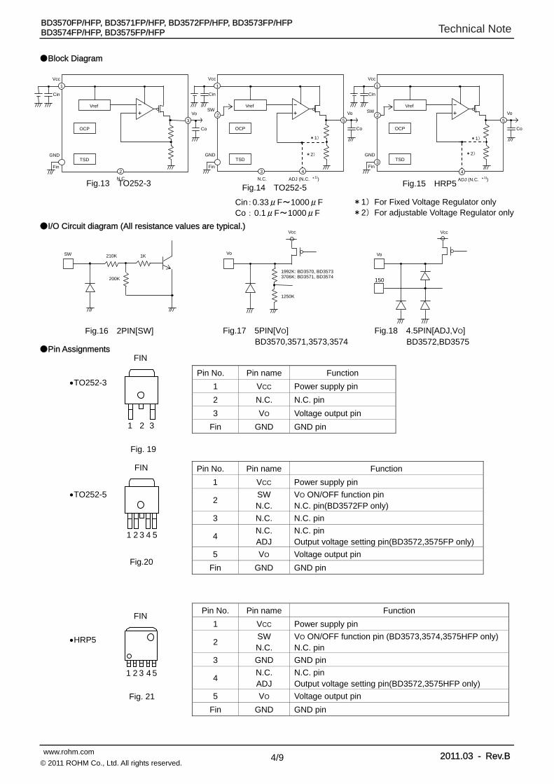
●Block Diagram
●I/O Circuit diagram (All resistance values are typical.)
●Pin Assignments
TO252-3
TO252-5
HRP5
Pin No. Pin name Function
1 VCC Power supply pin
2 N.C. N.C. pin
3 VO Voltage output pin
Fin GND GND pin
Pin No. Pin name Function
1 VCC Power supply pin
2 SW N.C.
VO ON/OFF function pin N.C. pin(BD3572FP only)
3 N.C. N.C. pin
4 N.C. ADJ
N.C. pin Output voltage setting pin(BD3572,3575FP only)
5 VO Voltage output pin
Fin GND GND pin
Pin No. Pin name Function
1 VCC Power supply pin
2 SW N.C.
VO ON/OFF function pin (BD3573,3574,3575HFP only) N.C. pin
3 GND GND pin
4 N.C. ADJ
N.C. pin Output voltage setting pin(BD3572,3575HFP only)
5 VO Voltage output pin
Fin GND GND pin
1 2 3
FIN
Fig. 19
FIN
1 2 3 4 5
Fig.20
Fig. 21
1 2 3 4 5
FIN
GND
Vcc
Vref
OCP
TSD
Vo
Fin
1
N.C.
2
3
Cin
Fig.13 TO252-3
Cin:0.33μF~1000μFCo:0.1μF~1000μF
Co
Fig.14 TO252-5
Vo
Co
ADJ (N.C. *1))
GND
Vcc
Vref
OCP
TSD
Fin
1
5
Cin
4
*1)
*2)
2SW
GND
Vref
OCP
TSD
Vo
5
Co
4Fin
SW2
3
N.C. ADJ (N.C. *1))
*1)
*2)
*1)For Fixed Voltage Regulator only *2)For adjustable Voltage Regulator only
Fig.15 HRP5
Vcc
1
Cin
3
Fig.16 2PIN[SW]
SW 210K 1K
200K
Fig.17 5PIN[VO] BD3570,3571,3573,3574
Vcc
Vo
1992K: BD3570, BD35733706K: BD3571, BD3574
1250K
Fig.18 4.5PIN[ADJ,VO] BD3572,BD3575
Vcc
Vo
150

Technical Note
5/9
BD3570FP/HFP, BD3571FP/HFP, BD3572FP/HFP, BD3573FP/HFP BD3574FP/HFP, BD3575FP/HFP
www.rohm.com 2011.03 - Rev.B© 2011 ROHM Co., Ltd. All rights reserved.
●Output Voltage Adjustment
To set the output voltage insert pull-down resistor R1 between the ADJ and GND pins, and pull-up resistor R2 between the VO and ADJ pins.
Vo = VADJ×(R1+R2) / R1 [V] {VADJ=1.26V(TYP.)}
The recommended connection resistor for the ADJ-GND is 30k~150kΩ.
●Setting of Heat TO252-3 TO252-5 HRP5
Fig. 23 Fig. 24 Fig. 25
Refer to the heat mitigation characteristics illustrated in Figs. 23, 24 and 25 when using the IC in an environment where Ta
≧25℃. The characteristics of the IC are greatly influenced by the operating temperature. If the temperature is in excess of the maximum junction temperature Tjmax, the elements of the IC may be deteriorated or damaged. It is necessary to give sufficient consideration to the heat of the IC in view of two points, i.e., the protection of the IC from instantaneous damage and the maintenance of the reliability of the IC in long-time operation. In order to protect the IC from thermal destruction, it is necessary to operate the IC not in excess of the maximum junction temperature Tjmax. Fig. 23 illustrates the power dissipation/heat mitigation characteristics for the TO252 package. Operate the IC within the power dissipation Pd. The following method is used to calculate the power consumption PC (W).
Vcc : Input voltage
PC=(VCC-VO)×IO+VCC×ICC Vo : Output voltage
Power dissipation Pd≦PC Io : Load current Icc : Total supply current
The load current IO is obtained to operate the IC within the power dissipation.
(For more information about ICC, see page 12.)
The maximum load current Iomax for the applied voltage VCC can be calculated during the thermal design process.
●Calculation example Example: BD3571FP VCC = 12 V and VO = 5 V at Ta = 85℃
IO≦89mA (ICC=30μA)
Make a thermal calculation in consideration of the above so that the whole operating temperature range will be within the power dissipation. The power consumption Pc of the IC in the event of shorting (i.e., if the VO and GND pins are shorted) will be obtained from the following equation.
Pc=VCC×(ICC+Ishort) Ishort = Short current
VCC-VO Io≦ Pd-VCC×ICC
IO≦ 0.624-12×ICC
12-5
θja=104.2℃/W→-9.6mAW/℃25℃=1.2W→85℃=0.624W
0
0.4
1.2 W
0
0.8
1.2
1.6
2.0
25 50 75 100 125 150
IC mounted on a ROHM standard board Substrate size: 70 mm 70 mm 1.6 mm ja = 104.2 (°C/W)
AMBIENT TEMPERATURE: Ta [°C]
PO
WE
R D
ISS
IPA
TIO
N:
Pd
[W
]
0
0.4
1.6 W
0
0.8
1.2
1.6
2.0
25 50 75 100 125 150
IC mounted on a ROHM standard board Substrate size: 70 mm 70 mm 1.6 mmja = 78.1 (°C/W)
AMBIENT TEMPERATURE: Ta [°C]
PO
WE
R D
ISS
IPA
TIO
N:
Pd
[W
]
0
0.4
1.3W
0
0.8
1.2
1.6
2.0
25 50 75 100 125 150
AMBIENT TEMPERATURE: Ta [℃]
PO
WE
R D
ISS
IPA
TIO
N:
Pd
[W
] IC mounted on a ROHM standard board
Substrate size: 70 mm 70 mm 1.6 mm ja = 96.2 (°C/W)
Fig.22
ADJ
Vo
R2
R1
Technical Note
6/9
BD3570FP/HFP, BD3571FP/HFP, BD3572FP/HFP, BD3573FP/HFP BD3574FP/HFP, BD3575FP/HFP
www.rohm.com 2011.03 - Rev.B© 2011 ROHM Co., Ltd. All rights reserved.
●Peripheral Settings for Pins and Precautions 1) VCC pins
Insert capacitors with a capacitance of 0.33μF to 1000μF between the VCC and GND pins. The capacitance varies with the application. Be sure to design the capacitance with a sufficient margin.
2) Capacitors for stopping oscillation for output pins
Capacitors for stopping oscillation must be placed between each output pin and the GND pin. Use a capacitor within a capacitance range between 0.1μF and 1000μF. Since oscillation does not occur even for ESR values from 0.001Ω to 100Ω, a ceramic capacitor can be used. Abrupt input voltage and load fluctuations can affect output voltages. Output capacitor capacitance values should be determined after sufficient testing of the actual application.
●Operation Notes 1) Absolute maximum ratings
Use of the IC in excess of absolute maximum ratings such as the applied voltage or operating temperature range may result in IC damage. Assumptions should not be made regarding the state of the IC (short mode or open mode) when such damage is suffered. A physical safety measure such as a fuse should be implemented when use of the IC in a special mode where the absolute maximum ratings may be exceeded is anticipated.
2) GND potential
Ensure a minimum GND pin potential in all operating conditions. 3) Setting of heat
Use a thermal design that allows for a sufficient margin in light of the power dissipation (Pd) in actual operating conditions. 4) Pin short and mistake fitting
Use caution when orienting and positioning the IC for mounting on printed circuit boards. Improper mounting may result in damage to the IC. Shorts between output pins or between output pins and the power supply and GND pins caused by the presence of a foreign object may result in damage to the IC.
5) Actions in strong magnetic field
Use caution when using the IC in the presence of a strong magnetic field as doing so may cause the IC to malfunction. 6) Testing on application boards
When testing the IC on an application board, connecting a capacitor to a pin with low impedance subjects the IC to stress. Always discharge capacitors after each process or step. Be sure to turn power off when mounting or dismounting jigs at the inspection stage. Furthermore, for countermeasures against static electricity, ground the equipment at the assembling stage and pay utmost attention at the time of transportation or storing the product.
7) This monolithic IC contains P+ isolation and P substrate layers between adjacent elements in order to keep them isolated.
PN junction is formed by the P layer and the N layer of each element, and a variety of parasitic elements will be constituted. For example, when a resistor and transistor are connected to pins as shown in Fig. 19,
the P/N junction functions as a parasitic diode when GND>Pin A for the resistor or GND>Pin B for the transistor (NPN).
Similarly, when GND>Pin B for the transistor (NPN), the parasitic diode described above combines with the N layer of other adjacent elements to operate as a parasitic NPN transistor.

Technical Note
7/9
BD3570FP/HFP, BD3571FP/HFP, BD3572FP/HFP, BD3573FP/HFP BD3574FP/HFP, BD3575FP/HFP
www.rohm.com 2011.03 - Rev.B© 2011 ROHM Co., Ltd. All rights reserved.
The formation of parasitic elements as a result of the relationships of the potentials of different pins is an inevitable result of the IC's architecture. The operation of parasitic elements can cause interference with circuit operation as well as IC malfunction and damage. For these reasons, it is necessary to use caution so that the IC is not used in a way that will trigger the operation of parasitic elements, such as by the application of voltages lower than the GND (P substrate) voltage to input pins.
Fig. 26 Example of a Simple Monolithic IC Architecture
8) Ground wiring patterns
When using both small signal and large current GND patterns, it is recommended to isolate the two ground patterns, placing a single ground point at the application's reference point so that the pattern wiring resistance and voltage variations caused by large currents do not cause variations in the small signal ground voltage. Be careful not to change the GND wiring pattern of any external parts, either.
9) SW Pin Do not apply the voltage to SW pin when the VCC is not applied. And when the VCC is applied, the voltage of SW pin must not exceed VCC.
10) Thermal shutdown circuit (TSD) This IC incorporates a built-in thermal shutdown circuit for the protection from thermal destruction. The IC should be used within the specified power dissipation range. However, in the event that the IC continues to be operated in excess of its power dissipation limits, the attendant rise in the chip's temperature Tj will trigger the thermal shutdown circuit to turn off all output power elements. The circuit automatically resets once the chip's temperature Tj drops. The thermal shutdown circuit operates if the IC is under conditions in express of the absolute maximum ratings. Never design sets on the premise of using the thermal shutdown circuit. (See Fig. 8)
11) Overcurrent protection circuit (OCP) The IC incorporates a built-in overcurrent protection circuit that operates according to the output current capacity. This circuit serves to protect the IC from damage when the load is shorted. The protection circuit is designed to limit current flow by not latching in the event of a large and instantaneous current flow originating from a large capacitor or other component. These protection circuits are effective in preventing damage due to sudden and unexpected accidents. However, the IC should not be used in applications characterized by the continuous operation or transitioning of the protection circuits. At the time of thermal designing, keep in mind that the current capability has negative characteristics to temperatures. (See Fig. 3)
GND
N
P
N N
P+ P+
Parasitic elementor transistor
P substrt
(Pin B) CB
E
Transistor (NPN)
(Pin A)
GND
N
P
N N
P+ P+
Resistor
Parasitic element P
Parasitic elements
(Pin A)
Parasitic element ortransistor
(Pin B)
GND
CB
E
Technical Note
8/9
BD3570FP/HFP, BD3571FP/HFP, BD3572FP/HFP, BD3573FP/HFP BD3574FP/HFP, BD3575FP/HFP
www.rohm.com 2011.03 - Rev.B© 2011 ROHM Co., Ltd. All rights reserved.
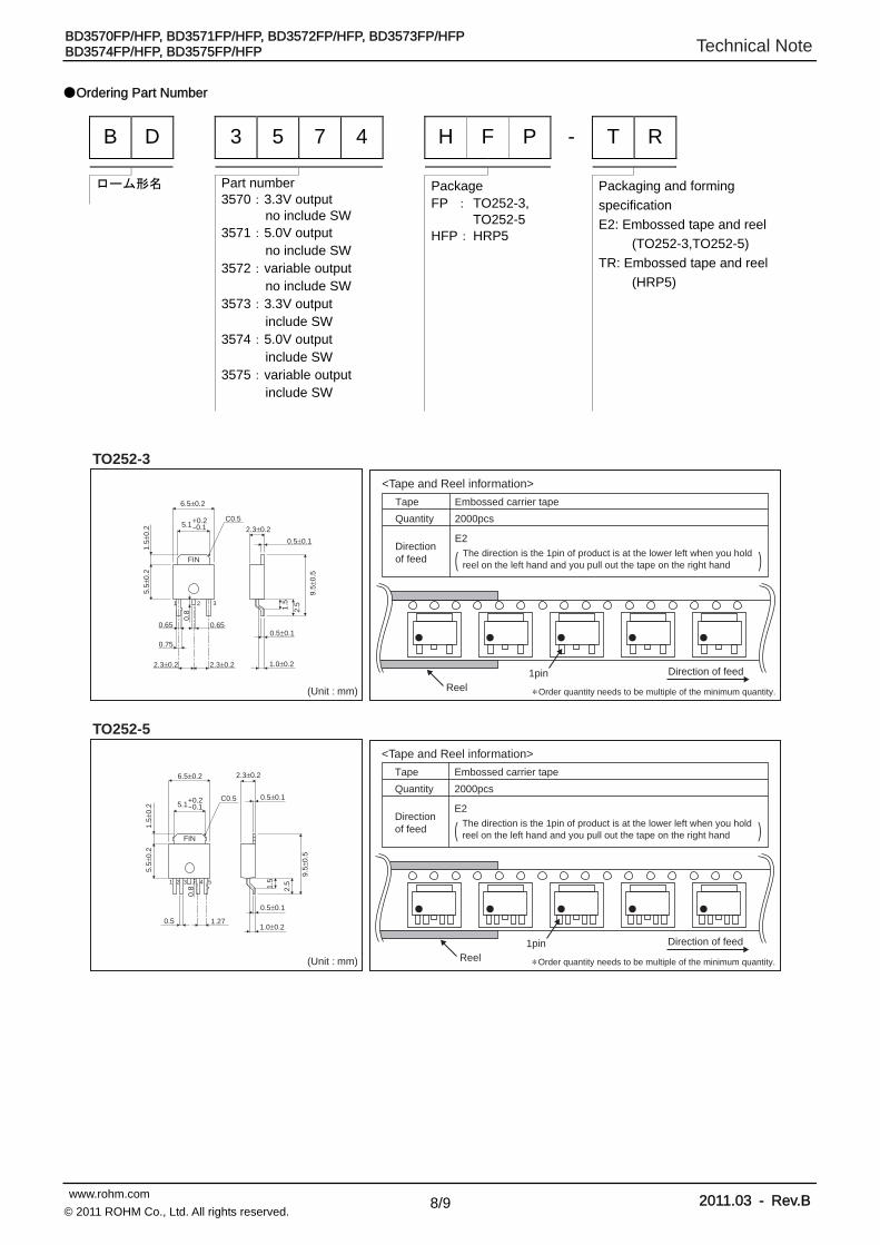
●Ordering Part Number
B D 3 5 7 4 H F P - T R
ローム形名 Part number
3570:3.3V output no include SW 3571:5.0V output no include SW 3572:variable output no include SW 3573:3.3V output include SW 3574:5.0V output include SW 3575:variable output include SW
Package FP : TO252-3, TO252-5 HFP: HRP5
Packaging and forming
specification
E2: Embossed tape and reel
(TO252-3,TO252-5)
TR: Embossed tape and reel
(HRP5)
(Unit : mm)
TO252-3
21 3
0.8
0.65 0.65
1.5
2.5
0.75
FIN
6.5±0.2
2.3±0.2 2.3±0.2
0.5±0.1
1.0±0.2
2.3±0.2
9.5±
0.5
0.5±0.1
5.5±
0.2
1.5±
0.2 5.1+0.2
-0.1C0.5
Direction of feed1pinReel ∗ Order quantity needs to be multiple of the minimum quantity.
<Tape and Reel information>
Embossed carrier tapeTape
Quantity
Direction of feed
The direction is the 1pin of product is at the lower left when you hold reel on the left hand and you pull out the tape on the right hand
2000pcs
E2
( )
(Unit : mm)
TO252-5
1 2 3 54
0.8
0.5 1.27
1.5
2.5
FIN
6.5±0.2 2.3±0.2
0.5±0.1
1.0±0.2
9.5±
0.5
0.5±0.1
5.5±
0.2
1.5±
0.2
C0.55.1+0.2
-0.1
Direction of feed1pinReel ∗ Order quantity needs to be multiple of the minimum quantity.
<Tape and Reel information>
Embossed carrier tapeTape
Quantity
Direction of feed
The direction is the 1pin of product is at the lower left when you hold reel on the left hand and you pull out the tape on the right hand
2000pcs
E2
( )

Technical Note
9/9
BD3570FP/HFP, BD3571FP/HFP, BD3572FP/HFP, BD3573FP/HFP BD3574FP/HFP, BD3575FP/HFP
www.rohm.com 2011.03 - Rev.B© 2011 ROHM Co., Ltd. All rights reserved.
Direction of feed
1pin
Reel ∗ Order quantity needs to be multiple of the minimum quantity.
<Tape and Reel information>
Embossed carrier tapeTape
Quantity
Direction of feed
2000pcs
TR
( )The direction is the 1pin of product is at the upper right when you hold reel on the left hand and you pull out the tape on the right hand
(Unit : mm)
HRP5
S
0.08 S
(MAX 9.745 include BURR)
54321
1.905±0.1
0.83
5±0.
21.
523±
0.15
10.5
4±0.
13−0.05+0.1
0.27
4.5°
(6.5)8.82 ± 0.1
9.395±0.125
0.73±0.11.72
0.08
±0.0
5
(7.4
9)
8.0±
0.13
1.01
7±0.
2
1.2575−4.5°+5.5°
DatasheetDatasheet
Notice - GE Rev.002© 2014 ROHM Co., Ltd. All rights reserved.
Notice Precaution on using ROHM Products
1. Our Products are designed and manufactured for application in ordinary electronic equipments (such as AV equipment, OA equipment, telecommunication equipment, home electronic appliances, amusement equipment, etc.). If you intend to use our Products in devices requiring extremely high reliability (such as medical equipment (Note 1), transport equipment, traffic equipment, aircraft/spacecraft, nuclear power controllers, fuel controllers, car equipment including car accessories, safety devices, etc.) and whose malfunction or failure may cause loss of human life, bodily injury or serious damage to property (“Specific Applications”), please consult with the ROHM sales representative in advance. Unless otherwise agreed in writing by ROHM in advance, ROHM shall not be in any way responsible or liable for any damages, expenses or losses incurred by you or third parties arising from the use of any ROHM’s Products for Specific Applications.
(Note1) Medical Equipment Classification of the Specific Applications JAPAN USA EU CHINA
CLASSⅢ CLASSⅢ
CLASSⅡb CLASSⅢ
CLASSⅣ CLASSⅢ
2. ROHM designs and manufactures its Products subject to strict quality control system. However, semiconductor
products can fail or malfunction at a certain rate. Please be sure to implement, at your own responsibilities, adequate safety measures including but not limited to fail-safe design against the physical injury, damage to any property, which a failure or malfunction of our Products may cause. The following are examples of safety measures:
[a] Installation of protection circuits or other protective devices to improve system safety [b] Installation of redundant circuits to reduce the impact of single or multiple circuit failure
3. Our Products are designed and manufactured for use under standard conditions and not under any special or extraordinary environments or conditions, as exemplified below. Accordingly, ROHM shall not be in any way responsible or liable for any damages, expenses or losses arising from the use of any ROHM’s Products under any special or extraordinary environments or conditions. If you intend to use our Products under any special or extraordinary environments or conditions (as exemplified below), your independent verification and confirmation of product performance, reliability, etc, prior to use, must be necessary:
[a] Use of our Products in any types of liquid, including water, oils, chemicals, and organic solvents [b] Use of our Products outdoors or in places where the Products are exposed to direct sunlight or dust [c] Use of our Products in places where the Products are exposed to sea wind or corrosive gases, including Cl2,
H2S, NH3, SO2, and NO2
[d] Use of our Products in places where the Products are exposed to static electricity or electromagnetic waves [e] Use of our Products in proximity to heat-producing components, plastic cords, or other flammable items [f] Sealing or coating our Products with resin or other coating materials [g] Use of our Products without cleaning residue of flux (even if you use no-clean type fluxes, cleaning residue of
flux is recommended); or Washing our Products by using water or water-soluble cleaning agents for cleaning residue after soldering
[h] Use of the Products in places subject to dew condensation
4. The Products are not subject to radiation-proof design. 5. Please verify and confirm characteristics of the final or mounted products in using the Products. 6. In particular, if a transient load (a large amount of load applied in a short period of time, such as pulse. is applied,
confirmation of performance characteristics after on-board mounting is strongly recommended. Avoid applying power exceeding normal rated power; exceeding the power rating under steady-state loading condition may negatively affect product performance and reliability.
7. De-rate Power Dissipation (Pd) depending on Ambient temperature (Ta). When used in sealed area, confirm the actual
ambient temperature. 8. Confirm that operation temperature is within the specified range described in the product specification. 9. ROHM shall not be in any way responsible or liable for failure induced under deviant condition from what is defined in
this document.
Precaution for Mounting / Circuit board design 1. When a highly active halogenous (chlorine, bromine, etc.) flux is used, the residue of flux may negatively affect product
performance and reliability. 2. In principle, the reflow soldering method must be used; if flow soldering method is preferred, please consult with the
ROHM representative in advance. For details, please refer to ROHM Mounting specification

DatasheetDatasheet
Notice - GE Rev.002© 2014 ROHM Co., Ltd. All rights reserved.
Precautions Regarding Application Examples and External Circuits 1. If change is made to the constant of an external circuit, please allow a sufficient margin considering variations of the
characteristics of the Products and external components, including transient characteristics, as well as static characteristics.
2. You agree that application notes, reference designs, and associated data and information contained in this document
are presented only as guidance for Products use. Therefore, in case you use such information, you are solely responsible for it and you must exercise your own independent verification and judgment in the use of such information contained in this document. ROHM shall not be in any way responsible or liable for any damages, expenses or losses incurred by you or third parties arising from the use of such information.
Precaution for Electrostatic
This Product is electrostatic sensitive product, which may be damaged due to electrostatic discharge. Please take proper caution in your manufacturing process and storage so that voltage exceeding the Products maximum rating will not be applied to Products. Please take special care under dry condition (e.g. Grounding of human body / equipment / solder iron, isolation from charged objects, setting of Ionizer, friction prevention and temperature / humidity control).
Precaution for Storage / Transportation 1. Product performance and soldered connections may deteriorate if the Products are stored in the places where:
[a] the Products are exposed to sea winds or corrosive gases, including Cl2, H2S, NH3, SO2, and NO2 [b] the temperature or humidity exceeds those recommended by ROHM [c] the Products are exposed to direct sunshine or condensation [d] the Products are exposed to high Electrostatic
2. Even under ROHM recommended storage condition, solderability of products out of recommended storage time period may be degraded. It is strongly recommended to confirm solderability before using Products of which storage time is exceeding the recommended storage time period.
3. Store / transport cartons in the correct direction, which is indicated on a carton with a symbol. Otherwise bent leads
may occur due to excessive stress applied when dropping of a carton. 4. Use Products within the specified time after opening a humidity barrier bag. Baking is required before using Products of
which storage time is exceeding the recommended storage time period.
Precaution for Product Label QR code printed on ROHM Products label is for ROHM’s internal use only.
Precaution for Disposition When disposing Products please dispose them properly using an authorized industry waste company.
Precaution for Foreign Exchange and Foreign Trade act Since our Products might fall under controlled goods prescribed by the applicable foreign exchange and foreign trade act, please consult with ROHM representative in case of export.
Precaution Regarding Intellectual Property Rights 1. All information and data including but not limited to application example contained in this document is for reference
only. ROHM does not warrant that foregoing information or data will not infringe any intellectual property rights or any other rights of any third party regarding such information or data. ROHM shall not be in any way responsible or liable for infringement of any intellectual property rights or other damages arising from use of such information or data.:
2. No license, expressly or implied, is granted hereby under any intellectual property rights or other rights of ROHM or any
third parties with respect to the information contained in this document.
Other Precaution 1. This document may not be reprinted or reproduced, in whole or in part, without prior written consent of ROHM. 2. The Products may not be disassembled, converted, modified, reproduced or otherwise changed without prior written
consent of ROHM. 3. In no event shall you use in any way whatsoever the Products and the related technical information contained in the
Products or this document for any military purposes, including but not limited to, the development of mass-destruction weapons.
4. The proper names of companies or products described in this document are trademarks or registered trademarks of
ROHM, its affiliated companies or third parties.

DatasheetDatasheet
Notice – WE Rev.001© 2014 ROHM Co., Ltd. All rights reserved.
General Precaution 1. Before you use our Pro ducts, you are requested to care fully read this document and fully understand its contents.
ROHM shall n ot be in an y way responsible or liabl e for fa ilure, malfunction or acci dent arising from the use of a ny ROHM’s Products against warning, caution or note contained in this document.
2. All information contained in this docume nt is current as of the issuing date and subj ect to change without any prior
notice. Before purchasing or using ROHM’s Products, please confirm the la test information with a ROHM sale s representative.
3. The information contained in this doc ument is provi ded on an “as is” basis and ROHM does not warrant that all
information contained in this document is accurate an d/or error-free. ROHM shall not be in an y way responsible or liable for any damages, expenses or losses incurred by you or third parties resulting from inaccuracy or errors of or concerning such information.