Hi-Rel PNP bipolar transistor -80 V, -5 A · Hi-Rel PNP bipolar transistor -80 V, -5 A Datasheet...
16
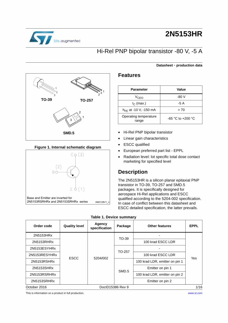
This is information on a product in full production. October 2016 DocID15386 Rev 9 1/16 2N5153HR Hi-Rel PNP bipolar transistor -80 V, -5 A Datasheet - production data Figure 1. Internal schematic diagram Features • Hi-Rel PNP bipolar transistor • Linear gain characteristics • ESCC qualified • European preferred part list - EPPL • Radiation level: lot specific total dose contact marketing for specified level Description The 2N5153HR is a silicon planar epitaxial PNP transistor in TO-39, TO-257 and SMD.5 packages. It is specifically designed for aerospace Hi-Rel applications and ESCC qualified according to the 5204-002 specification. In case of conflict between this datasheet and ESCC detailed specification, the latter prevails. TO-39 SMD.5 TO-257 AM3128V1_n Base and Emitter are inverted for 2N5153RSRHRx and 2N5153SRHRx series Parameter Value V CEO -80 V I C (max.) -5 A h FE at -10 V, -150 mA > 70 Operating temperature range -65 °C to +200 °C Table 1. Device summary Order code Quality level Agency specification Package Other features EPPL 2N5153HRx ESCC 5204/002 TO-39 - Yes 2N5153RHRx 100 krad ESCC LDR 2N5153ESYHRx TO-257 - 2N5153RESYHRx 100 krad ESCC LDR 2N5153RSHRx SMD.5 100 krad LDR, emitter on pin 1 2N5153SHRx Emitter on pin 1 2N5153RSRHRx 100 krad LDR, emitter on pin 2 2N5153SRHRx Emitter on pin 2 www.st.com
Transcript of Hi-Rel PNP bipolar transistor -80 V, -5 A · Hi-Rel PNP bipolar transistor -80 V, -5 A Datasheet...
This is information on a product in full production.
October 2016 DocID15386 Rev 9 1/16
2N5153HR
Hi-Rel PNP bipolar transistor -80 V, -5 A
Datasheet - production data
Figure 1. Internal schematic diagram
Features
• Hi-Rel PNP bipolar transistor
• Linear gain characteristics
• ESCC qualified
• European preferred part list - EPPL
• Radiation level: lot specific total dose contact marketing for specified level
DescriptionThe 2N5153HR is a silicon planar epitaxial PNP transistor in TO-39, TO-257 and SMD.5 packages. It is specifically designed for aerospace Hi-Rel applications and ESCC qualified according to the 5204-002 specification. In case of conflict between this datasheet and ESCC detailed specification, the latter prevails.
TO-39
SMD.5
TO-257
AM3128V1_n
Base and Emitter are inverted for2N5153RSRHRx and 2N5153SRHRx series
Parameter Value
VCEO -80 V
IC (max.) -5 A
hFE at -10 V, -150 mA > 70
Operating temperature range
-65 °C to +200 °C
Table 1. Device summary
Order code Quality levelAgency
specificationPackage Other features EPPL
2N5153HRx
ESCC 5204/002
TO-39-
Yes
2N5153RHRx 100 krad ESCC LDR
2N5153ESYHRxTO-257
-
2N5153RESYHRx 100 krad ESCC LDR
2N5153RSHRx
SMD.5
100 krad LDR, emitter on pin 1
2N5153SHRx Emitter on pin 1
2N5153RSRHRx 100 krad LDR, emitter on pin 2
2N5153SRHRx Emitter on pin 2
www.st.com
Contents 2N5153HR
2/16 DocID15386 Rev 9
Contents
1 Electrical ratings . . . . . . . . . . . . . . . . . . . . . . . . . . . . . . . . . . . . . . . . . . . . 3
2 Electrical characteristics . . . . . . . . . . . . . . . . . . . . . . . . . . . . . . . . . . . . . 4
3 Electrical characteristics (curves) . . . . . . . . . . . . . . . . . . . . . . . . . . . . . . 5
3.1 Test circuit . . . . . . . . . . . . . . . . . . . . . . . . . . . . . . . . . . . . . . . . . . . . . . . . . 6
4 Radiation hardness assurance . . . . . . . . . . . . . . . . . . . . . . . . . . . . . . . . 7
5 Package information . . . . . . . . . . . . . . . . . . . . . . . . . . . . . . . . . . . . . . . . . 8
5.1 TO-257 package information . . . . . . . . . . . . . . . . . . . . . . . . . . . . . . . . . . . 8
5.2 TO-39 package information . . . . . . . . . . . . . . . . . . . . . . . . . . . . . . . . . . . 10
5.3 SMD.5 package information . . . . . . . . . . . . . . . . . . . . . . . . . . . . . . . . . . . .11
6 Ordering information . . . . . . . . . . . . . . . . . . . . . . . . . . . . . . . . . . . . . . . 12
7 Shipping details . . . . . . . . . . . . . . . . . . . . . . . . . . . . . . . . . . . . . . . . . . . . 14
7.1 Date code . . . . . . . . . . . . . . . . . . . . . . . . . . . . . . . . . . . . . . . . . . . . . . . . . 14
7.2 Documentation . . . . . . . . . . . . . . . . . . . . . . . . . . . . . . . . . . . . . . . . . . . . . 14
8 Revision history . . . . . . . . . . . . . . . . . . . . . . . . . . . . . . . . . . . . . . . . . . . 15
DocID15386 Rev 9 3/16
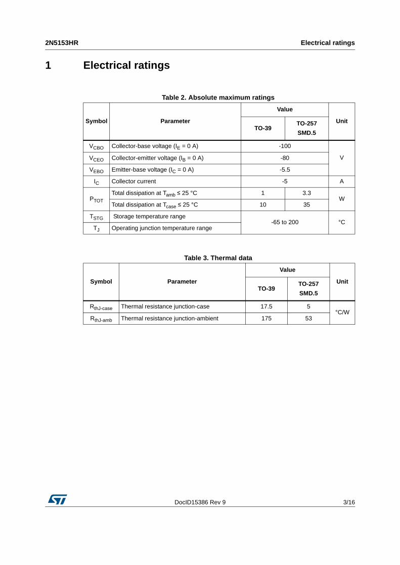
2N5153HR Electrical ratings
16
1 Electrical ratings
Table 2. Absolute maximum ratings
Symbol Parameter
Value
UnitTO-39
TO-257
SMD.5
VCBO Collector-base voltage (IE = 0 A) -100
VVCEO Collector-emitter voltage (IB = 0 A) -80
VEBO Emitter-base voltage (IC = 0 A) -5.5
IC Collector current -5 A
PTOT
Total dissipation at Tamb ≤ 25 °C 1 3.3W
Total dissipation at Tcase ≤ 25 °C 10 35
TSTG Storage temperature range-65 to 200 °C
TJ Operating junction temperature range
Table 3. Thermal data
Symbol Parameter
Value
UnitTO-39
TO-257
SMD.5
RthJ-case Thermal resistance junction-case 17.5 5°C/W
RthJ-amb Thermal resistance junction-ambient 175 53
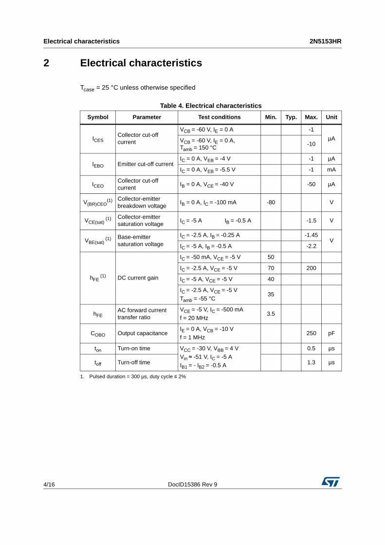
Electrical characteristics 2N5153HR
4/16 DocID15386 Rev 9
2 Electrical characteristics
Tcase = 25 °C unless otherwise specified
Table 4. Electrical characteristics
Symbol Parameter Test conditions Min. Typ. Max. Unit
ICESCollector cut-off current
VCB = -60 V, IE = 0 A -1
µAVCB = -60 V, IE = 0 A, Tamb = 150 °C
-10
IEBO Emitter cut-off currentIC = 0 A, VEB = -4 V -1 µA
IC = 0 A, VEB = -5.5 V -1 mA
ICEOCollector cut-off current
IB = 0 A, VCE = -40 V -50 µA
V(BR)CEO(1)
1. Pulsed duration = 300 µs, duty cycle ≤ 2%
Collector-emitter breakdown voltage
IB = 0 A, IC = -100 mA -80 V
VCE(sat) (1) Collector-emitter
saturation voltageIC = -5 A IB = -0.5 A -1.5 V
VBE(sat) (1) Base-emitter
saturation voltage
IC = -2.5 A, IB = -0.25 A -1.45V
IC = -5 A, IB = -0.5 A -2.2
hFE (1) DC current gain
IC = -50 mA, VCE = -5 V 50
IC = -2.5 A, VCE = -5 V 70 200
IC = -5 A, VCE = -5 V 40
IC = -2.5 A, VCE = -5 V
Tamb = -55 °C35
hFEAC forward current transfer ratio
VCE = -5 V, IC = -500 mA
f = 20 MHz3.5
COBO Output capacitanceIE = 0 A, VCB = -10 V
f = 1 MHz250 pF
ton Turn-on time VCC = -30 V, VBB = 4 V
Vin ≈ -51 V, IC = -5 AIB1 = - IB2 = -0.5 A
0.5 µs
toff Turn-off time 1.3 µs
DocID15386 Rev 9 5/16
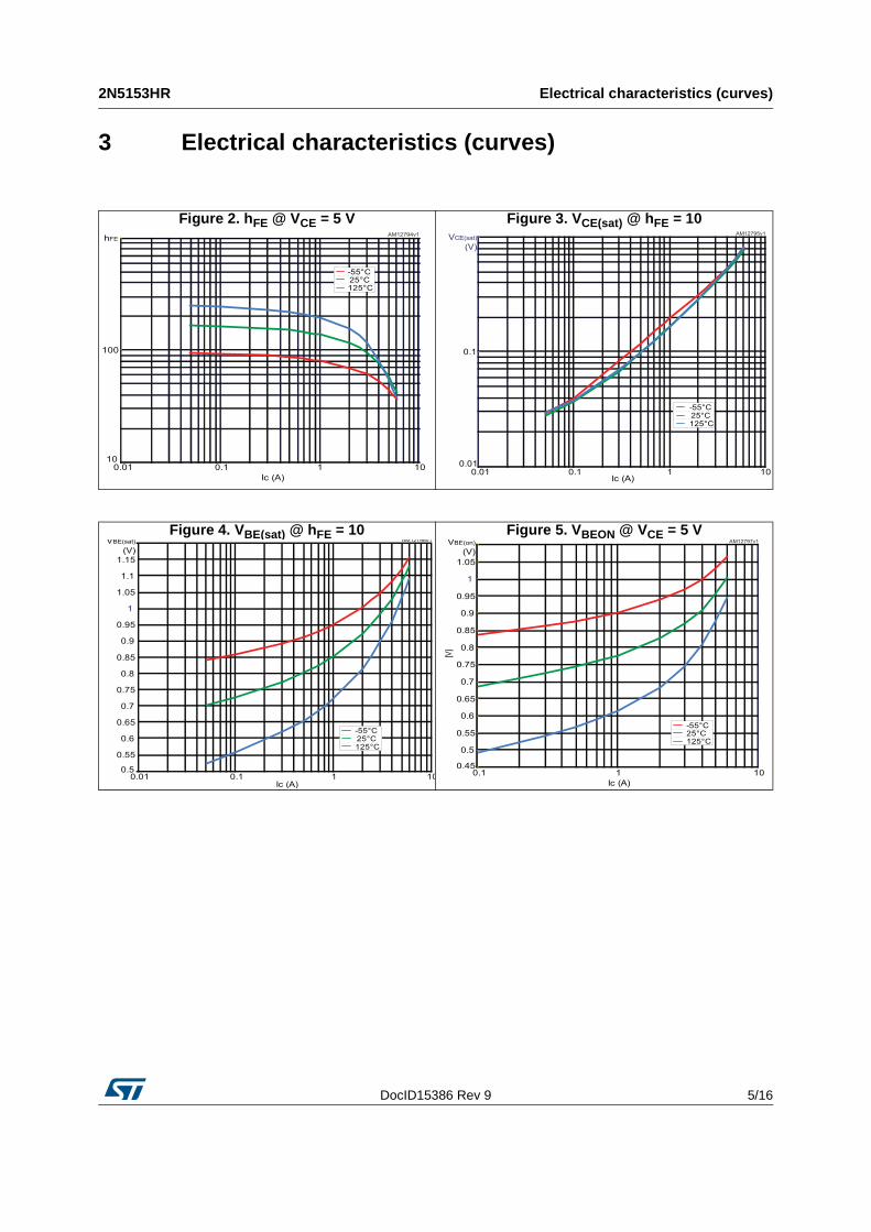
2N5153HR Electrical characteristics (curves)
16
3 Electrical characteristics (curves)
Figure 2. hFE @ VCE = 5 V Figure 3. VCE(sat) @ hFE = 10AM12794v1
Ic (A)0.01 0.1 1 10
10
100
hFE
-55°C25°C125°C
AM12795v1
0.01 0.1 1 100.01
0.1
VCE(sat)
(V)
-55°C25°C125°C
Ic (A)
Figure 4. VBE(sat) @ hFE = 10 Figure 5. VBEON @ VCE = 5 VAM12796v1
Ic (A)0.01 0.1 1 10
VBE(sat)
(V)1.15
1.1
1.05
1
0.95
0.9
0.85
0.8
0.75
0.7
0.65
0.6
0.55
0.5
-55°C25°C125°C
AM12797v1
Ic (A)0.1 1 10
[V]
VBE(on)
(V)1.05
1
0.95
0.9
0.85
0.8
0.75
0.7
0.65
0.6
0.55
0.5
0.45
-55°C25°C125°C
Electrical characteristics (curves) 2N5153HR
6/16 DocID15386 Rev 9
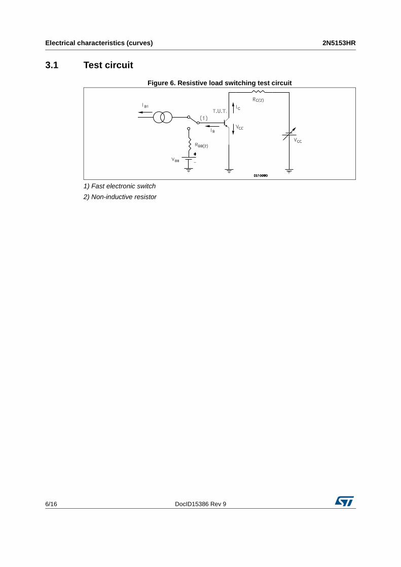
3.1 Test circuit
Figure 6. Resistive load switching test circuit
1) Fast electronic switch
2) Non-inductive resistor
DocID15386 Rev 9 7/16
2N5153HR Radiation hardness assurance
16
4 Radiation hardness assurance
The products guaranteed in radiation within the ESCC system fully comply with the ESCC 5204/002 and ESCC 22900 specifications.
ESCC radiation assurance
Each product lot is tested according to the ESCC basic specification 22900, with a minimum of 11 samples per diffusion lot and 5 samples per wafer, one sample being kept as unirradiated sample, all of them being fully compliant with the applicable ESCC generic and/or detailed specification.
ST goes beyond the ESCC specification by performing the following procedure:
– 11 pieces per wafer tested, 5 biased at least 80% of V(BR)CEO, 5 unbiased and 1 kept for reference
– Irradiation at 0.1 rad (Si)/s
– Acceptance criteria of each individual wafer if as 100 krad guaranteed if all 10 samples comply with the post radiation electrical characteristics provided in Table 5
Delivery together with the parts of the radiation verification test (RVT) report of the particular wafer used to manufacture the products. This RVT includes the value of each parameter at 30, 50, 70 and 100 krad (Si) and after 24 hour annealing at room temperature and after an additional 168 hour annealing at 100 °C.
Table 5. ESCC 5204/002 post radiation electrical characteristics
Symbol Parameter Test conditions Min. Typ. Max. Unit
ICESCollector cut-off current
IE = 0 A, VCB = -60 V
-
-1 µA
IEBO Emitter cut-off currentIC = 0 A, VEB = -4 V -1 µA
IC = 0 A, VEB = -5.5 V -1 mA
ICEOCollector cut-off current
IB = 0 A, VCE = -40 V -50 µA
V(BR)CEO (1)
1. Pulsed duration = 300 µs, duty cycle ≤ 2%.
Collector-emitter breakdown voltage
IB = 0 A, IC = -100 mA -80 V
VCE(sat) (1) Collector-emitter
saturation voltageIC = -5 A, IB = -0.5 A -1.5 V
VBE(sat) (1) Base-emitter
saturation voltage
IC = -2.5 A, IB = -0.25 A -1.45V
IC = -5 A, IB = -0.5 A -2.2
[hFE] (1) Post irradiation gain
calculation(2)
2. The post-irradiation gain calculation of [hFE], made using hFE measurements from prior to and on completion of irradiation testing and after each annealing step if any, is as specified in MILSTD-750 method 1019.
IC = -50 mA, VCE = -5 V [25]
IC = -2.5 A, VCE = -5 V [35] [200]
IC = -5 A, VCE = -5 V [20]
Package information 2N5153HR
8/16 DocID15386 Rev 9
5 Package information
In order to meet environmental requirements, ST offers these devices in different grades of ECOPACK® packages, depending on their level of environmental compliance. ECOPACK® specifications, grade definitions and product status are available at: www.st.com. ECOPACK® is an ST trademark.
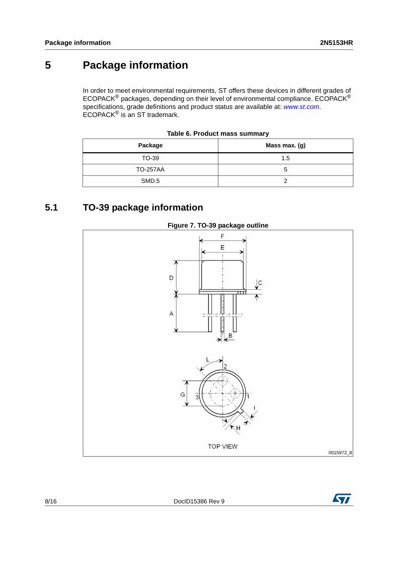
5.1 TO-39 package information
Figure 7. TO-39 package outline
Table 6. Product mass summary
Package Mass max. (g)
TO-39 1.5
TO-257AA 5
SMD.5 2
0015972_8
DocID15386 Rev 9 9/16
2N5153HR Package information
16
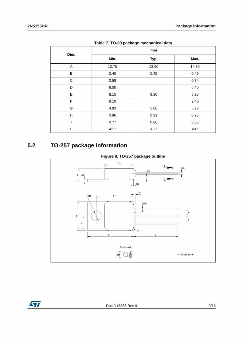
5.2 TO-257 package information
Figure 8. TO-257 package outline
Table 7. TO-39 package mechanical data
Dim.mm
Min. Typ. Max.
A 12.70 13.50 14.30
B 0.40 0.45 0.49
C 0.58 0.74
D 6.00 6.40
E 8.15 8.20 8.25
F 9.10 9.40
G 4.93 5.08 5.23
H 0.86 0.91 0.96
I 0.77 0.80 0.86
L 42 ° 45 ° 48 °
0117268 rev 6
Package information 2N5153HR
10/16 DocID15386 Rev 9
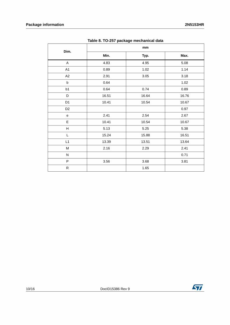
Table 8. TO-257 package mechanical data
Dim.mm
Min. Typ. Max.
A 4.83 4.95 5.08
A1 0.89 1.02 1.14
A2 2.91 3.05 3.18
b 0.64 1.02
b1 0.64 0.74 0.89
D 16.51 16.64 16.76
D1 10.41 10.54 10.67
D2 0.97
e 2.41 2.54 2.67
E 10.41 10.54 10.67
H 5.13 5.25 5.38
L 15.24 15.88 16.51
L1 13.39 13.51 13.64
M 2.16 2.29 2.41
N 0.71
P 3.56 3.68 3.81
R 1.65

DocID15386 Rev 9 11/16
2N5153HR Package information
16
5.3 SMD.5 package information
Figure 9. SMD.5 package outline
Table 9. SMD.5 package mechanical data
Dim.mm Inch
Min. Typ. Max. Min. Typ. Max.
A 2.84 3.00 3.15 0.112 0.118 0.124
A1 0.25 0.38 0.51 0.010 0.015 0.020
b 7.13 7.26 7.39 0.281 0.286 0.291
b1 5.58 5.72 5.84 0.220 0.225 0.230
b2 2.28 2.41 2.54 0.090 0.095 0.100
b3 2.92 3.05 3.18 0.115 0.120 0.125
D 10.03 10.16 10.28 0.935 0.400 0.405
D1 0.76 0.030
E 7.39 7.52 7.64 0.291 0.296 0.301
e 1.91 0.075
7386434 rev 5
Pin 1 indicator

Ord
ering
info
rmatio
n2N
5153HR
12/16D
ocID15386 R
ev 9
6 Ordering information
Table 10. Order code
Order codeAgency
specificationEPPL Quality level Other features Package
Lead finish
Marking(1) Packing
2N51531 - -Engineering
model-
TO-39
Gold 2N51531
Strip pack
2N5153HRG 5204/002/01 Yes ESCC - Gold 520400201
2N5153HRT 5204/002/02 Yes ESCC - Solder dip 520400202
2N5153RHRG 5204/002/01R Yes ESCC 100 krad ESCC LDR Gold 520400201R
2N5153RHRT 5204/002/02R Yes ESCC 100 krad ESCC LDR Solder dip 520400202R
2N5153ESY1 - -Engineering
model-
TO-257
Gold 2N5153ESY1 + BeO
2N5153ESYHRG 5204/002/04 Yes ESCC - Gold 520400204 + BeO
2N5153ESYHRT 5204/002/05 Yes ESCC - Solder dip 520400205 + BeO
2N5153RESYHRG 5204/002/04R Yes ESCC 100 krad ESCC LDR Gold 520400204R + BeO
2N5153RESYHRT 5204/002/05R Yes ESCC 100 krad ESCC LDR Solder dip 520400205R + BeO
2N5153S1 - -Engineering
modelEmitter on pin 1
SMD.5 Gold
2N5153S1
2N5153RSHRG 5204/002/06R Yes ESCC100 krad LDR, emitter
on pin 1520400206R
2N5153SHRG 5204/002/06 Yes ESCC Emitter on pin 1 520400206
2N5153SR1 - -Engineering
modelEmitter on pin 2 2N5153SR1
2N5153RSRHRG 5204/002/07R Yes ESCC100 krad LDR, emitter
on pin 2520400207R
2N5153SRHRG 5204/002/07 Yes ESCC Emitter on pin 2 520400207
1. Specific marking only. The full marking includes in addition, for the engineering models: ST logo, date code, country of origin (FR). For ESCC flight parts: ST logo, datecode, country of origin (FR), ESA logo, serial number of the part within the assembly lot.
DocID15386 Rev 9 13/16
2N5153HR Ordering information
16
Contact ST sales office for information about the specific conditions for:
• Products in die form
• Tape and reel packing

Shipping details 2N5153HR
14/16 DocID15386 Rev 9
7 Shipping details
7.1 Date codeDate code xyywwz is structured as per the table below:
7.2 Documentation
Table 11. Date code
Type x yy ww z
EM (ESCC) 3 Last two digits of the year
Week digitsLot index within the weekESCC flight
Table 12. Documentation provided for each type of product
Quality level Radiation level Documentation
Engineering model Last two digits of the year
ESCC flight 100 krad
Certificate of conformance
0.1 rad/s radiation verification test report
DocID15386 Rev 9 15/16
2N5153HR Revision history
16
8 Revision history
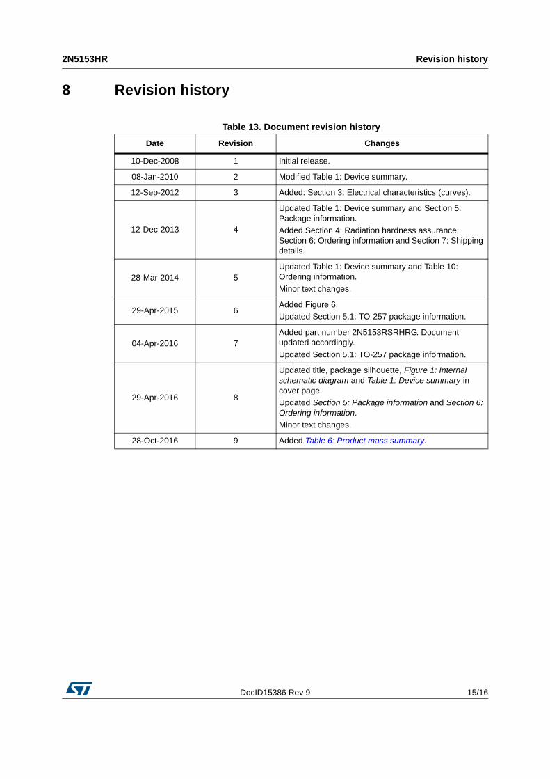
Table 13. Document revision history
Date Revision Changes
10-Dec-2008 1 Initial release.
08-Jan-2010 2 Modified Table 1: Device summary.
12-Sep-2012 3 Added: Section 3: Electrical characteristics (curves).
12-Dec-2013 4
Updated Table 1: Device summary and Section 5: Package information.Added Section 4: Radiation hardness assurance, Section 6: Ordering information and Section 7: Shipping details.
28-Mar-2014 5Updated Table 1: Device summary and Table 10: Ordering information.Minor text changes.
29-Apr-2015 6Added Figure 6.Updated Section 5.1: TO-257 package information.
04-Apr-2016 7Added part number 2N5153RSRHRG. Document updated accordingly.
Updated Section 5.1: TO-257 package information.
29-Apr-2016 8
Updated title, package silhouette, Figure 1: Internal schematic diagram and Table 1: Device summary in cover page.Updated Section 5: Package information and Section 6: Ordering information.Minor text changes.
28-Oct-2016 9 Added Table 6: Product mass summary.
2N5153HR
16/16 DocID15386 Rev 9
IMPORTANT NOTICE – PLEASE READ CAREFULLY
STMicroelectronics NV and its subsidiaries (“ST”) reserve the right to make changes, corrections, enhancements, modifications, and improvements to ST products and/or to this document at any time without notice. Purchasers should obtain the latest relevant information on ST products before placing orders. ST products are sold pursuant to ST’s terms and conditions of sale in place at the time of order acknowledgement.
Purchasers are solely responsible for the choice, selection, and use of ST products and ST assumes no liability for application assistance or the design of Purchasers’ products.
No license, express or implied, to any intellectual property right is granted by ST herein.
Resale of ST products with provisions different from the information set forth herein shall void any warranty granted by ST for such product.
ST and the ST logo are trademarks of ST. All other product or service names are the property of their respective owners.
Information in this document supersedes and replaces information previously supplied in any prior versions of this document.
© 2016 STMicroelectronics – All rights reserved


![[PPT]Bipolar Junction Transistors: Basics - University of …people.virginia.edu/~ag7rq/663/Fall10/lec13_BJT.ppt · Web viewECE 663 Common Base DC current gain - PNP Common Base –](https://static.fdocuments.us/doc/165x107/5ade367c7f8b9ae1408e12ba/pptbipolar-junction-transistors-basics-university-of-ag7rq663fall10lec13bjtpptweb.jpg)