Pb-Free High Temperature Solder Joints for Power Semiconductor ...
Application of the Advanced Activator Technology on Halogen-Free Lead-Free
Solder Paste Development
Xiang Wei, Ph.D.
Adrian Hawkins, Ph.D.
Kester, Inc
Itasca, Illinois
ABSTRACT:
The Surface Mount Technology (SMT) industry has been faced with several challenges in the past decades. Two of the most
recent ones are RoHS compliant lead-free assembly and the adoption of fine-pitch components assembly processes.
Moreover, halogen-free is another new requirement for assembled PCB reliability, environmental and health concerns. All
these requirements create fundamental challenges of developing a solder paste to satisfy everything. One of the resolutions
for these challenges can be the development of the activator package with the advanced organic chemistry technology.
Serial innovative activator system was developed recently for solder paste flux, tacky flux and liquid flux formulation. This
paper will discuss three Type 4 lead-free halogen-free no-clean solder pastes (ROL0) developed based on different innovative
activators, which respond to the challenges described above. The printing performance, coalescence, wetting, BGA voiding
and head-in-pillow characteristics, are compared and discussed in detail. The testing results show all three pastes with the
new activators are fully capable of printing and reflowing 01005 components with different board/device finishes, even in air
reflow. They can handle a wide variety of print variables, including print speed, long abandon time and a wide range of
temperature and humidity. Post-soldering, the paste offers minimized defects, including head-in-pillow and BGA voiding.
Key Words: miniature and fine pitch components, halogen-free, lead-free, solder paste, activator, voiding, head-in-pillow
INTRODUCTION:
Three of the most recent SMT challenges are RoHS compliant lead-free assembly, the adoption of fine-pitch components,
and halogen-free requirement. Solder paste, as one of the major contributors affecting all SMT process and defect ratio, has
been pushed to the far front to meet all these requirements.
The majority lead-free alloys in the current market are Sn-Ag-Cu (SAC) alloys, which have melting point around 217-227C,
34C higher than eutectic Sn63Pb37. This higher melting range requires the solder paste to be reflowed at higher peak
temperatures in the range of 235-245C with longer time, while still able to maintain enough paste flux activity to remove
oxides, prevent bridging and dripping, enable spread and wicking, and decrease voiding. Particularly for the larger board
designed with castle-sized devices, the heating time has been extended much longer to prevent thermal shock and minimize
the voiding, which makes it more challenging for the flux to maintain enough activity during this process.
Fine-pitch components used today include 01005 and 0201 passives, 0.15mm-0.4mm CSP and BGA, and 14-20mil pitch
QFP/QFN. In order to obtain the appropriate and consistent paste release on these fine pad sizes, the stencil thickness
dropped from 8mil to 3mi, and the powder size used in the solder paste dropped from Type 3 (T3 25µm-45µm) to Type 4 (T4
20µm-38µm) and even down to Type 5 (T5 15µm -25µm), according to the surface tension and aspect ratio as well as five
solder particles rule. The finer particles have larger surface area and the oxidation is more significant in air reflow than that
of bigger particles, which requires the solder flux to have higher activity to remove the oxides on the powder surface and
prevent oxidation in the later stages of the reflow process as well. The other side effect of the finer particles is the increase of
cohesion in the solder paste, which has negative impact on the stencil release and requires more efforts on the chemical
reaction control and rheology optimization. Furthermore, the solder paste deposit on the smaller pads has a much larger ratio
of the surface area to the flux volume, which makes it harder for the flux to clean the oxides on the powder, pad and device
surface. The insufficient fluxing will cause poor wetting, solder balling, voiding or un-coalesced solder particles, that is,
“graping” defect. The severe “graping” defect will lead to the mechanical and electrical reliability issues.
The last requirement is coming from major OEMs in US, Japan and Europe, which have been moving from “lead-free” to
“halogen-free” as part of their environmental friendly campaigns, per “Guide to Greener Electronics” issued by
GREENPEACE. In traditional solder pastes, the halogen-contained activator is used to achieve high flux activity to remove
oxides and promote solder wetting. Halogen-free requires totally different design of the activator package, which must
provide equivalent or even higher activity than halogen-contained ones.

The detailed requirement/challenges for formulating a new solder paste can be summarized as:
1. In compliance with halogen-free and RoHS lead-free
2. Appropriate rheoloy with finer power particles for consistent print release for fine-pitch components, and minimum
1 hour abandon time with 25-150mm/s print speeds
3. Sufficient flux activity to provide excellent solderability under higher and longer reflowing process in air
4. Excellent solderability with different surface finishes
5. Maintain or even improve reliability while addressing all of the above
6. Low voiding, head-in-pillow, tombstoning and other defects.
7. Compatible with conformal coating
8. Compatible with both open squeegee and enclosed print heads, e.g. DEK ProFlow and MPM Rheopump
9. ICT (In Circuit Test)-friendly residue
10. Good cleanability or removal of residues, if required.
In order to meet all these requirements, a serial of innovative activator system was developed recently for solder paste flux,
tacky flux and liquid flux formulation. These activators are designed to be activated at different temperature range according
to the thermal profile and application requirements. The fluxing mechanisms are able to perform at multiple stages to remove
oxides and prevent further oxidation from the beginning to the end of the reflowing process. Besides the fluxing application,
the flux chemistry and reaction kinetics are also designed to minimize by-products for no-clean category, or yield water-
soluble by-products for cleanable products, from the chemical reactions between the flux and oxides, as well as between flux
and metal surface. This way, the residue corrosion behavior and cleanability are under control. The by-product effect on the
surface tension, contributing to the wetting performance, is also under consideration during paste formulating. Meanwhile,
the activators with hydrophilic property are used for water soluble products and non-hydrophilic ones are used for no-clean
products.
This paper will discuss three T4 halogen-free lead-free no-clean solder pastes (ROL0) developed based on different
innovative activators. Mixture DOE (Design of Experiment) has been applied during formulating, and most requirements
presented above were used as the model responses. The optimized formula was created from the model to achieve the best
combination of all performance requirements. The printing performance, coalescence, wetting, BGA voiding and head-in-
pillow characteristics, and SIR/ECM reliability test (Surface Insulation Resistivity and Electrochemical Migration) will be
discussed in detail.
EXPERIMENT DESIGN
The pastes evaluated and discussed here consist of three LF HF no-clean T4 solder pastes DA1, DA2 and DA3. All these
pastes are classified as type ROL0 per IPC J-STD-004B. An extensive printing study has been designed and performed to
evaluate the paste capability under a wide variety of printing variables, including duration, abandon time, different speed and
environment conditions.
4mil and 5mil laser cut fine grain stencils, 220mm squeegee with edge guards, side foil clamps, and universal blocks tooling
were used on a Speedline MPM Momentum stencil printer. For most tests, the printing speed was set at 50mm/sec and the
board separation speed is 10mm/sec. The printing environment was controlled at around 22°C and 40%rh by a DEK
environmental control unit.
An 200mm x 254mm test vehicle with Cu OSP finish was used, which has 18868 data points consisting of 0.15mm - 0.50mm
BGA circles and squares, 0201 - 2512 passives, 20mil pitch QFP/QFN, CTBGA228 (0.5mm pitch), and 6.5mm wetting
circles. The selected pad sizes and area ratio are listed in Table 1. ENIG and immersion silver finish boards were also used
for coalescence and wetting analysis.
A Koh Young KY- 3020T laser solder paste inspection system was used to measure the volume of the paste deposits. A Gage
Repeatability and Reproducibility analysis was performed before the printing test to ensure the precision results.
The printed boards were reflowed in a Speedline OmniExcel 7 Reflow Oven for coalescence and wetting analysis. Two
reflow profiles under air atmosphere and three finishing boards (Cu OSP, ENIG and immersion Ag) were used. A 2D X-ray
inspection system was used for BGA voiding evaluation. Head-in-pillow test were performed at Jabil Circuit.

Table 1 - Printing Test Vehicle Pad Design
Test Locations
Aperture Size Area Ratio Stencil
Opening :
Pad Size
Solder Mask
Defined Width
(mm)
Length
(mm)
Pitch size
(mm)
4mil
stencil
5mil
stencil
0.25mm BGA 0.25 - 0.60 0.615 0.492 1:1 Y
0.30mm BGA 0.30 - 0.70 0.750 0.600 1:1 Y
0.50mm BGA 0.50 - 0.90 1.230 0.984 1:1 Y
CTBGA228 0.35 - 0.50 0.861 0.689 1:1 Y
Chip 0201 0.34 0.38 - 0.883 0.706 1:1 N
Chip 0402 0.38 0.40 - 0.959 0.767 1:1 N
QFP32 (20mil) 1.05 0.25 0.50 0.994 0.795 1:1 N
MLF32 (20mil) 0.75 0.25 0.50 0.923 0.738 1:1 N
6.5mm Wetting Pad 6.5 - - 15.99 12.80 1:1 Y
RESULTS AND DISCUSSION
Printability
Figure 1 shows the printing transfer efficiency of three pastes on the selected pad sizes. Each data set includes 20 boards’
Koh Young inspection data. All pastes have release capability down to 0.25mm BGA (9.8mil pad size) with 4mil stencil,
pushing the area ratio down to ~0.60. DA1 has slightly better release than DA2 and DA3 on the finer pitch release. For 0.25
and 0.30mm BGA, the square apertures have slightly lower transfer efficiency than the circle apertures, but with smaller
standard deviation and better print definition, indicating that square shape helps paste release better than the circle. The
lower transfer efficiency is due to peaking phenomena on circle pads (increasing paste height), as well as volume%
calculation method for the rounded corner of square apertures. The 20mil QFN (MLF) has a larger deviation than 20mil QFP
due to the different pad configuration. The paste capability to avoid bridging and stencil cleaning frequency were evaluated
on 20mil QFP/QFNs pads. 20 boards were printed continuously without stencil cleaning. No bridging was noted within 10
boards for all these pastes.
Figure 1 - Printing Transfer Efficiency of DA1, DA2 and DA3 with 4mil Stencil.
The paste has been kneading on the stencil around 8 hours and 10 boards were printed after each hour to evaluate paste
durability on the stencil. The stencil was vacuum/dry cleaned right before the board was printed. Figure 2 shows DA1 and
DA2 stencil life on 4mil stencil, as well as DA3 on 5mil stencil. The printing release is consistent during 8 hours printing for
all three products. The pastes exhibited good rolling and release definition, and didn’t show signs of drying or degradation.
IPC solderball, slump and tackiness tests were also performed every 2 hours and the data was consistent from the beginning
to the end of durability test.

Figure 2 - Solder Paste Stencil Life: (A) DA1 and (B) DA2 with 4mil Stencil; (C) DA3 with 5mil Stencil
The paste recovery performance has been evaluated after it was abandoned on the stencil from one to three hours. Figure 3
presents 1h recovery performance of DA1, DA2 and DA3. From 0.25mm to 6.5mm pads, the first board of all three pastes is
capable to achieve over 70% transfer efficiency after abandoned 1h on the stencil. DA1 and DA2 have slightly better
recovery performance than DA3. All three pastes are capable of recovery around the first or second boards with over 70%
transfer efficiency after 2-3 hours abandon time. The pastes showed no sign of dry out.

Figure 3 – DA1, DA2 and DA3 Solder Paste Recovery Performance after Abandoned 1h on the Stencil.
DA1 was also printed under different speeds and environmental conditions. The consistent releasing data, shown in Figure 4,
indicates DA1 is capable of printing from 50 to 150mm/s speed and at different temperature and humidity conditions. The
environment test data has slightly larger deviation since each set includes 40 board data points for four hours print durability
test. DA2 and DA3 are under evaluation and the higher humidity level 65% will be used as well. DA1 printing performance
in DEK Proflow and MPM Rheopump were also evaluated. The print definition and transfer efficiency is excellent; no
compaction or significant flux separation was observed.
Figure 4 – DA1 Solder Paste Print Performance under Different Speed and Environment Conditions.
Reflow Performance
As explained previously, the most significant challenge for the new solder paste is to provide enough activity to produce a
solid and reliable solder joint, but still meet all halogen-free, lead-free, fine pitch release, and good electric reliability
requirements. In this study, two profiles, listed in Figure 5, were used for coalescence and wetting evaluation under air
atmosphere. “Pb-Free Long” profile provides more challenges for the solder paste since oxidation increases more rapidly and
flux activity decreases with the longer heating time. Table 2 gives an example of DA1 coalescence behavior on 0.25mm
BGA with Cu OSP, ENIG and immersion Ag finish boards reflowed in air. DA2 and DA3 have very similar coalescence

behavior. No graping was observed for all three pastes down to 0.25mm BGA with three different finishes and two profiles
in air reflow. Besides insufficient flux activity, graping can also be due to poor printing release, an extreme situation with
much larger surface area with less flux volume. The solderability differences among three pastes are under evaluation on
0.20mm BGA on 3mil stencil printed boards.
Profiles Max (+)
Slope
Max (-)
Slope
Time 150-
217C (S)
Time >217
C
Peak
Temp. 217C /
Peak
Peak \
217C
Pb-Free Long 1.94 -2.33 100 58 243 0.74 -0.82
Pb-Free MID 3.70 -6.20 75 59 245 0.86 -1.11
Figure 5 – Reflow Profiles.
Table 2 – DA1 Coalescence of 0.25mm BGA Solder Joint in Air Reflow
Profile Cu OSP ENIG Immersion Ag
MID
LONG
The wetting performance was evaluated by measuring the wetting length of the air-reflowed paste on the rectangular pads,
and the printed paste length is 1mm. Figure 6 shows the variability plot of three pastes’ wetting length on Cu OSP, ENIG
and immersion Ag finishes. The board finishes have significant effect on the paste wetting performance. The pastes have the
best wetting performance on ENIG, and the worst on Cu OSP, consistent with the recent solderability study on different
board finishes. [1] On EING board, the wetting ability is following DA1>DA2>DA3; DA1 and DA3 have better wetting
than DA2 on Ag boards; and thee pastes have equivalent wetting performance on Cu OSP boards.
Head-in-Pillow and BGA Voiding
Head-in-Pillow (HiP) defects, in Figure 7, are formed due to the component warpage, resulting in less contact or separation
of solder balls and the paste. At the higher reflow temperature, the surface of the solder ball is oxidized, but the paste cannot
wet the solder ball and is reflowed by itself, causing the formation of two separated solder joints during cooling. One of the
resolutions to mitigate HiP defect is to maintain enough flux activity at higher temperature and improve the solder paste
wetting performance, that is, wicking up the solder ball quickly. The innovative activator packages are designed to meet this
requirement. DA1 head-in-pillow test was performed at Jabil Circuit, San Jose, with the method presented in IPC/APEX
2011. [2] In a total of 10 tested coupons, DA1 has 8 full coalesced solder joints with fast wetting and only 2 partially
coalesced solder joints. With 84% rating, it has the best wetting and soldering performance to mitigate HiP defects compared
to the other products tested in Jabil. [2]

Figure 6 – Wetting Analysis.
Figure 7 - Head-in-Pillow Solder Joint Optical Images. Left: Full Coalesced Solder Joint with Fast Wetting, Center:
Partial Coalesced Solder Joint, Right: Head-in-Pillow Defect
The BGA voiding of DA1 was evaluated on Cu OSP, immersion Sn and immersion Ag finished boards with Pb-free MID
profile, shown in Table 3. Cu OSP board shows the highest average void%, but all are far below 25% per IPC-7095A
specification. An extensive QFN voiding DOE for these paste products, involving different reflow profiles, board and
device finishes, and stencil design is under way. The test result will be shared in the near future.
Table 3 – DA1 BGA Voiding with Pb-free MID Profile, Three Lots Average
Pad Size 0.4mm BGA 0.625mm BGA
Board Finish OSP Immersion
Sn
Immersion
Ag OSP
Immersion
Sn
Immersion
Ag
Ave. Void % 2.85% 0.72% 1.34% 4.71% 4.58% 2.35%
Max. Void % 10.76% 4.96% 7.33% 13.16% 14.28% 10.71%

IPC Classification and Reliability
IPC SIR and ECM test results of DA1 and DA2 are shown in Figure 8, which exceed 108ohm and IRfinal IRintial/10 per J-
STD-004B requirement. The tested boards did not show signs for dendrites, discoloration or corrosion. DA3 was designed
for the different industry application and was evaluated with a special SIR profile, presented in Figure 9. Each point in the
curve presents the condensation point of the paste during temperature and humidity change. DA3 also meets 108ohm of J-
STD requirement and 5x10⁸ ohm of automotive industry requirement on no-clean solder paste under the special profile.
Boards: IPC-B-25, 3 boards/sample
Bias/Test Voltage: 10 / 100 Volts
Temperature/Humidity: 85°C/88.5%
IPC ECM 2.6.14.1 Control Ave. DA1 Ave. DA2 Ave.
IRintial (after 96 hours) 3.35E+10 1.81E+08 1.32E+09
IRfinal (after 596 hours) 2.58E+10 1.73E+08 1.20E+09
Figure 8 – IPC SIR and ECM for DA1 and DA2 solder paste via J-STD-004B
Figure 9 – DA3 10 Days SIR Test under the Special Profile

CONCLUSION
The current test results show that the innovative activator packages are capable of providing desired flux activity for the
developed solder pastes to meet not only J-STD and other reliability specifications, but also the most recent SMT
requirements as discussed previously. The printing and reflow performance of solder pastes DA1, DA2 and DA3 are
excellent. They can also help to mitigate the recent SMT defects issues, e.g. head-in-pillow and voiding. Further studies on
QFN/MLF voiding, ICT, and conformal coating compatibility will be carried out soon to fully understand the solder paste
performance.
ACKNOWLEDGEMENTS
The authors would like to thank the following group and individuals for their efforts and expertise during the solder paste
development and testing:
Quyen Chu and Sundar Sethuraman from Jabil Circuit for HiP test support
Hank Sanftleben and Scott Post from Delphi Electronics Group for the reliability test method and test vehicle
expertise and support.
Peter Biocca for his SMT expertise and support
Dinesh Amine and Kal Chokshi for the formula development and paste preparation during Mixture DOE.
Kyle Loomis and Paul Klimah for their great printing and reliability test support.
REFERENCES
[1]. Hunt, Chris. Zou, Ling. Adams, Sean. Board Finish Solderability with Sn-Ag-Cu; IPC SMEMA Council AMEX 2003;
presented in 2003.
[2]. Sethuraman, Sundar. Mitigating Head-in-Pillow Defects: an Experimental Approach to Identify No-Clean Soldering
Materials; IPC/APEX 2011; presented on April 12, 2011.

Halogen-free Lead-free Solder Paste With Advanced Activator Technology
Xiang Wei, Ph.D.
Kester, Inc. Itasca, IL
February 2012

Three Major SMT Challenges - Solder Paste Responses
Lead-Free Alloys Globally • Higher peak temperatures and longer heating time
• Sufficient flux activity
Fine Pitch Components: 01005, 0.15-0.4mm CSP & BGA, 14mil QFP • Smaller pads with larger ratio of the surface area to flux volume
• Type 4 and Type 5 finer solder powder with larger surface area and higher oxidation
• Sufficient flux activity to clean oxides and prevent poor wetting, solderball, and graping.
Halogen-Free per GREENPEACE • Equivalent or higher flux activity without halogen-contained chemicals

New Generation Solder Paste Requirements
Halogen and lead free
Consistent print release capability for fine-pitch components, and longer abandon time with 25-150mm/s print speeds
Sufficient flux activity to reflow in air with longer and higher temperature profile
Excellent solderability with different surface finishes
Maintain or even improve reliability while addressing all of the above
Low voiding, head-in-pillow, tombstoning and other defects
Compatible with conformal coating
Compatible with both open squeegee and enclosed print heads, e.g. DEK ProFlow and MPM Rheopump
ICT (In Circuit Test)-friendly residue
Good cleanability or removal of residues, if required

Activator Characteristics
Tuned for Thermal Profile
• Fluxing activity as a function of temperature
• Multiple-staged fluxing mechanisms
By-products Management through Flux Chemistry and Reaction
Kinetics
• Minimize by-products for no-clean category
• Yield water-soluble by-products for water-soluble products.
• Consider by-products effect on wetting and solderability performance
Hydrophilic or Non-hydrophilic for Different Applications

Experiment Design - Solder Pastes
Test Method Typical Data Paste Viscosity Malcom 10rpm 1450~1850 Poise IPC-Tack IPC2.4.44 ~40g IPC Solderball IPC2.4.43 Pass IPC Cold Slump IPC2.4.35 0.06, 0.00 IPC Hot Slump IPC2.4.35 0.20, 0.00 Residue Color Very Light and clear Residue Type Hard and Brittle Solder Joints Very Shiny Quantitative Halide IPC2.3.28.1 0.000% Copper Mirror (L,M,H) IPC2.3.32 L Copper Corrosion (L,M,H) IPC2.6.15 L
Surface Insulation Resistivity IPC2.6.3.7 Pass log(Ri) > 8
Electrochemical Migration IPC2.6.14.1 Pass
T4 Halogen-free Lead-free No-clean Solder Pastes: DA1, DA2 & DA3 IPC Classification: ROL0 Formula optimization by Mixture DOE with above requirements as responses Basic Properties

Equipments & Set-Up
6
• Printer & Stencil: MPM Momentum with laser-cut 4mil & 5mil
• Printing Speed: 50-150 mm/sec
• Test Vehicle: 200mm x 254mm with Cu OSP, Immersion Ag, ENIG finishes
• Environmental Control: 22°C & 40%RH
• Koh Young KY-3020 solder paste inspection & Electrovert OmniExcel 7 reflow oven
Test Locations Aperture Size Area Ratio Stencil
Opening : Pad Size
Solder Mask
Defined Width (mm) Length (mm) Pitch Size (mm) 4mil stencil 5mil stencil
0.25mm BGA 0.25 - 0.60 0.615 0.492 1:1 Y
0.30mm BGA 0.30 - 0.70 0.750 0.600 1:1 Y
0.50mm BGA 0.50 - 0.90 1.230 0.984 1:1 Y
CTBGA228 0.35 - 0.50 0.861 0.689 1:1 Y
Chip 0201 0.34 0.38 - 0.883 0.706 1:1 N
Chip 0402 0.38 0.40 - 0.959 0.767 1:1 N
QFP32 (20mil) 1.05 0.25 0.50 0.994 0.795 1:1 N
MLF32 (20mil) 0.75 0.25 0.50 0.923 0.738 1:1 N
Wetting Pad 6.5 - - 15.99 12.80 1:1 Y

Printability V
olum
e(%
)
0
20
40
60
80
10
12
14
16
DA
1
DA
2
DA
3
DA
1
DA
2
DA
3
DA
1
DA
2
DA
3
DA
1
DA
2
DA
3
DA
1
DA
2
DA
3
DA
1
DA
2
DA
3
DA
1
DA
2
DA
3
DA
1
DA
2
DA
3
DA
1
DA
2
DA
3
DA
1
DA
2
DA
3
0201ew 0402ew 05BGAc 025BGAc 030BGAc MLF32ew QFP32EW 025BGAsq 030BGAsq CTBGA228
Paste within PartNumber
Std
Dev
0
5
10
DA
1
DA
2
DA
3
DA
1
DA
2
DA
3
DA
1
DA
2
DA
3
DA
1
DA
2
DA
3
DA
1
DA
2
DA
3
DA
1
DA
2
DA
3
DA
1
DA
2
DA
3
DA
1
DA
2
DA
3
DA
1
DA
2
DA
3
DA
1
DA
2
DA
3
0201ew 0402ew 05BGAc 025BGAc 030BGAc MLF32ew QFP32EW 025BGAsq 030BGAsq CTBGA228
Paste within PartNumber
• Release capability down to 0.25mm BGA with 4mil stencil, area ratio ~0.6
• Criteria: >70% transfer efficiency & less than 20% deviation
• Square pads have slightly better release than circles ones.
• No bridging on 20mil QFP within 10 boards

Print Durability • Knead on the stencil for ~8 hours
• 10 boards were printed after each hour
• Release consistent, good rolling, no signs of drying or degradation
Vol
ume(
%)
0
30
60
90
12
15
0-In
itial 1h 2h 3h 6h 7h
0-In
itial 1h 2h 3h 6h 7h
0-In
itial 1h 2h 3h 6h 7h
0-In
itial 1h 2h 3h 6h 7h
0-In
itial 1h 2h 3h 6h 7h
0-In
itial 1h 2h 3h 6h 7h
0-In
itial 1h 2h 3h 6h 7h
0-In
itial 1h 2h 3h 6h 7h
0-In
itial 1h 2h 3h 6h 7h
0-In
itial 1h 2h 3h 6h 7h Durability
0201ew 0402ew 05BGAc 030BGAc MLF32ew QFP32EW 025BGAsq 030BGAsq 6_5mmcir CTBGA228 PartNumber
DA1 Paste
Std
Dev
0
10
0-In
itial 1h 2h 3h 6h 7h
0-In
itial 1h 2h 3h 6h 7h
0-In
itial 1h 2h 3h 6h 7h
0-In
itial 1h 2h 3h 6h 7h
0-In
itial 1h 2h 3h 6h 7h
0-In
itial 1h 2h 3h 6h 7h
0-In
itial 1h 2h 3h 6h 7h
0-In
itial 1h 2h 3h 6h 7h
0-In
itial 1h 2h 3h 6h 7h
0-In
itial 1h 2h 3h 6h 7h Durability
0201ew 0402ew 05BGAc 030BGAc MLF32ew QFP32EW 025BGAsq 030BGAsq 6_5mmcir CTBGA228 PartNumber
DA1 Paste

Print Durability - Continue
9
Volum
e(%
)
0
30
60
90
12
15
0-In
itial 1h 2h 3h 6h 7h
0-In
itial 1h 2h 3h 6h 7h
0-In
itial 1h 2h 3h 6h 7h
0-In
itial 1h 2h 3h 6h 7h
0-In
itial 1h 2h 3h 6h 7h
0-In
itial 1h 2h 3h 6h 7h
0-In
itial 1h 2h 3h 6h 7h
0-In
itial 1h 2h 3h 6h 7h
0-In
itial 1h 2h 3h 6h 7h
0-In
itial 1h 2h 3h 6h 7h Durability
0201ew 0402ew 05BGAc 030BGAc MLF32ew QFP32EW 025BGAsq 030BGAsq 6_5mmcir CTBGA228 PartNumber
DA2 Paste
Std
Dev
0
10
0-In
itial 1h 2h 3h 6h 7h
0-In
itial 1h 2h 3h 6h 7h
0-In
itial 1h 2h 3h 6h 7h
0-In
itial 1h 2h 3h 6h 7h
0-In
itial 1h 2h 3h 6h 7h
0-In
itial 1h 2h 3h 6h 7h
0-In
itial 1h 2h 3h 6h 7h
0-In
itial 1h 2h 3h 6h 7h
0-In
itial 1h 2h 3h 6h 7h
0-In
itial 1h 2h 3h 6h 7h Durability
0201ew 0402ew 05BGAc 030BGAc MLF32ew QFP32EW 025BGAsq 030BGAsq 6_5mmcir CTBGA228 PartNumber
DA2 Paste
Volum
e(%
)
0
20
40
60
80
10
12
14
0-ini
tial 1h 2h 3h 6h 7h
0-ini
tial 1h 2h 3h 6h 7h
0-ini
tial 1h 2h 3h 6h 7h
0-ini
tial 1h 2h 3h 6h 7h
0-ini
tial 1h 2h 3h 6h 7h
0-ini
tial 1h 2h 3h 6h 7h
0-ini
tial 1h 2h 3h 6h 7h
0-ini
tial 1h 2h 3h 6h 7h
0-ini
tial 1h 2h 3h 6h 7h
0-ini
tial 1h 2h 3h 6h 7h Druability
0201ew 0402ew 05BGAc 030BGAc MLF32ew QFP32EW 025BGAsq 030BGAsq 6_5mmcir CTBGA228 PartNumber
DA3 Paste
5mil Stencil
Std D
ev
0
15
30
0-ini
tial 1h 2h 3h 6h 7h
0-ini
tial 1h 2h 3h 6h 7h
0-ini
tial 1h 2h 3h 6h 7h
0-ini
tial 1h 2h 3h 6h 7h
0-ini
tial 1h 2h 3h 6h 7h
0-ini
tial 1h 2h 3h 6h 7h
0-ini
tial 1h 2h 3h 6h 7h
0-ini
tial 1h 2h 3h 6h 7h
0-ini
tial 1h 2h 3h 6h 7h
0-ini
tial 1h 2h 3h 6h 7h Druability
0201ew 0402ew 05BGAc 030BGAc MLF32ew QFP32EW 025BGAsq 030BGAsq 6_5mmcir CTBGA228 PartNumber
DA3 Paste
5mil Stencil

10
Print Recovery • 10 boards were printed after 1-3h abandon time
• Recovered at the 1st board with over 70% transfer efficiency after 1h abandon time for different pad sizes.
Volu
me(
%)
0
20
40
60
80
10
12
14
2999
3000
3001
3002
3003
3004
3005
3006
3007
3008
2092
2093
2094
2095
2096
2097
2098
2099
2100
2101
3101
3102
3103
3104
3105
3106
3107
3108
3109
3110
2999
3000
3001
3002
3003
3004
3005
3006
3007
3008
2092
2093
2094
2095
2096
2097
2098
2099
2100
2101
3101
3102
3103
3104
3105
3106
3107
3108
3109
3110
2999
3000
3001
3002
3003
3004
3005
3006
3007
3008
2092
2093
2094
2095
2096
2097
2098
2099
2100
2101
3101
3102
3103
3104
3105
3106
3107
3108
3109
3110
2999
3000
3001
3002
3003
3004
3005
3006
3007
3008
2092
2093
2094
2095
2096
2097
2098
2099
2100
2101
3101
3102
3103
3104
3105
3106
3107
3108
3109
3110
2999
3000
3001
3002
3003
3004
3005
3006
3007
3008
2092
2093
2094
2095
2096
2097
2098
2099
2100
2101
3101
3102
3103
3104
3105
3106
3107
3108
3109
3110 PCB ID
DA1 DA2 DA3 DA1 DA2 DA3 DA1 DA2 DA3 DA1 DA2 DA3 DA1 DA2 DA3 Paste
4mil 5mil 4mil 5mil 4mil 5mil 4mil 5mil 4mil 5mil Stencil
0201ew QFP32EW 025BGAsq 6_5mmcir CTBGA228 PartNumber
Std
Dev
0
15
30
2999
3000
3001
3002
3003
3004
3005
3006
3007
3008
2092
2093
2094
2095
2096
2097
2098
2099
2100
2101
3101
3102
3103
3104
3105
3106
3107
3108
3109
3110
2999
3000
3001
3002
3003
3004
3005
3006
3007
3008
2092
2093
2094
2095
2096
2097
2098
2099
2100
2101
3101
3102
3103
3104
3105
3106
3107
3108
3109
3110
2999
3000
3001
3002
3003
3004
3005
3006
3007
3008
2092
2093
2094
2095
2096
2097
2098
2099
2100
2101
3101
3102
3103
3104
3105
3106
3107
3108
3109
3110
2999
3000
3001
3002
3003
3004
3005
3006
3007
3008
2092
2093
2094
2095
2096
2097
2098
2099
2100
2101
3101
3102
3103
3104
3105
3106
3107
3108
3109
3110
2999
3000
3001
3002
3003
3004
3005
3006
3007
3008
2092
2093
2094
2095
2096
2097
2098
2099
2100
2101
3101
3102
3103
3104
3105
3106
3107
3108
3109
3110 PCB ID
DA1 DA2 DA3 DA1 DA2 DA3 DA1 DA2 DA3 DA1 DA2 DA3 DA1 DA2 DA3 Paste
4mil 5mil 4mil 5mil 4mil 5mil 4mil 5mil 4mil 5mil Stencil
0201ew QFP32EW 025BGAsq 6_5mmcir CTBGA228 PartNumber

Print Recovery - Continue
11
• 20 boards were printed after 3h abandon time for DA1
• Dry vacuum cleaning after every 10 boards printed
• Recovered at the 1st or 2nd board with over 70% transfer efficiency for different pad sizes.

Print Speed & Environmental Effects • Print speed: 50-150 mm/sec
• Temperature/Humidity: 22°C/25%rh, 22°C/45%rh, 27°C/22%rh
• Capable to handling with different print speed and temperature/humidity conditions.
Vol
ume(
%)
0
20
40
60
80
10
12
14
16
25% 45% 22% 25% 45% 22% 25% 45% 22% HUMIDITY
22C 27C 22C 27C 22C 27C TEMP
0201ew QFP32EW 035BGAsq PartNumber
Std
Dev
0
10
25% 45% 22% 25% 45% 22% 25% 45% 22% HUMIDITY
22C 27C 22C 27C 22C 27C TEMP
0201ew QFP32EW 035BGAsq PartNumber
Volu
me(
%)
0
20
40
60
80
10
12
14
050m
m/s
100m
m/s
150m
m/s
050m
m/s
100m
m/s
150m
m/s
050m
m/s
100m
m/s
150m
m/s
0201ew QFP32EW 025BGAsq
Speed within PartNumber
Std
Dev
0
10
050m
m/s
100m
m/s
150m
m/s
050m
m/s
100m
m/s
150m
m/s
050m
m/s
100m
m/s
150m
m/s
0201ew QFP32EW 025BGAsq
Speed within PartNumber

Reflow Performance Basic Coalescence & Wetting
• Two reflow profiles and three board finishes
• Check in-coalescence/grapping, separated solderballs and de-wetting
• Measure wetting length
Head-in-Pillow
• Evaluated by Jabil method* * Mitigating Head-in-Pillow Defects: an Experimental Approach to Identify
No-Clean Soldering Materials; IPC/APEX 2011
Voiding
• Three board finishes • X-ray 2D measurement

Reflow Profiles
Profiles Max (+) Slope
Max (-) Slope
Time 150-217°C (S)
Time >217°C
Peak Temp.
217°C / Peak
Peak \ 217°C
Pb-Free Long 1.94 -2.33 100 58 243 0.74 -0.82
Pb-Free MID 3.70 -6.20 75 59 245 0.86 -1.11

0.25mm BGA Coalescence in Air
15
Paste Profile Cu OSP ENIG Immers. Ag
DA1 MID
LONG
DA2 MID
LONG
DA3 MID
LONG
• No grapping down to 0.25mm BGA in air reflow.
• All three activator systems have sufficient activity for two reflow profiles and three board finishes.
• Coalescence on 0.20mm BGA with 3mil stencil is under evaluation.

Wetting Performance • Three finishes with MID file in air
• Printing Length: 1mm
• The spread length was measured under optical microscopy
• Best wetting on ENIG; worst on Cu OSP
• ENIG: DA1>DA2>DA3
• Similar activity on Cu and Ag.
Wet
ting
Leng
th (m
m)
0
0.5
1
1.5
2
2.5
DA1 DA2 DA3 DA1 DA2 DA3 DA1 DA2 DA3
Cu OSP ENIG Immersion Ag
Paste within Board Finish
Std
Dev
0.0
0.1
DA1 DA2 DA3 DA1 DA2 DA3 DA1 DA2 DA3
Cu OSP ENIG Immersion Ag
Paste within Board Finish

Head-in-Pillow HiP Defect Mechanism: Component warpage
Resolutions: • Minimize/control warpage
• Enlarge stencil aperture size
• Improve paste wetting with sufficient activity
Paste Evaluation Methods: • 10 samples for each paste
• Fresh Cu OSP board with 0.61mm BGA circle
• Solder ball: 0.76mm in diameter Pre-conditioned at 125°C for 24h
• 6mil laser-cut stencil
• Four categories:
Full coalescence with fast wetting Full coalescence with slow wetting Partial coalescence HiP Defect / No coalescence

Head-in-Pillow Test Method
1
2
3
* Sethuraman, Sundar. Mitigating Head-in-Pillow Defects: an Experimental Approach to Identify No-Clean Soldering Materials; IPC/APEX 2011

Head-in-Pillow Result • DA1 overall rating is 84%.
• Eight samples have full coalescence with fast wetting within 2 sec after contact; only two have partial coalescence.
• DA1 has sufficient activity and good wetting performance to mitigate HiP defects.
Full Coalescence Partial Coalescence
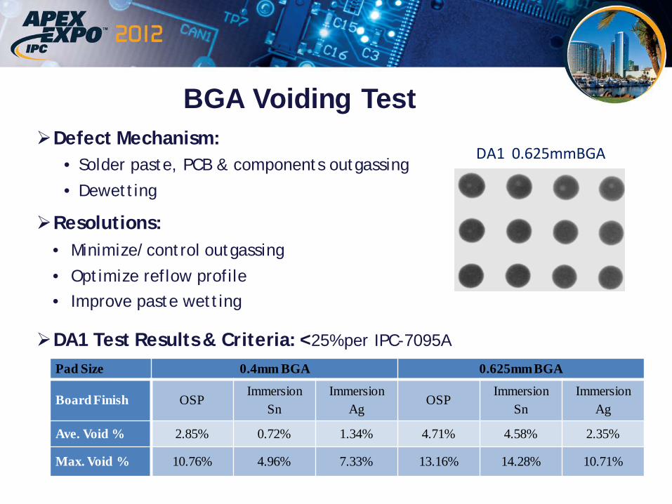
BGA Voiding Test Defect Mechanism:
• Solder paste, PCB & components outgassing
• Dewetting
Resolutions: • Minimize/control outgassing
• Optimize reflow profile • Improve paste wetting
DA1 Test Results & Criteria: <25% per IPC-7095A
20
Pad Size 0.4mm BGA 0.625mm BGA
Board Finish OSP Immersion
Sn Immersion
Ag OSP
Immersion Sn
Immersion Ag
Ave. Void % 2.85% 0.72% 1.34% 4.71% 4.58% 2.35%
Max. Void % 10.76% 4.96% 7.33% 13.16% 14.28% 10.71%
DA1 0.625mmBGA
IPC Reliability Test
Boards: IPC-B-25, 3 boards/sample Bias/Test Voltage: 10 / 100 Volts
Temperature/Humidity: 85°C/88.5%
IPC ECM 2.6.14.1 Control Ave. DA1 Ave. DA2 Ave. IRintial (after 96 hours) 3.35E+10 1.81E+08 1.32E+09 IRfinal (after 596 hours) 2.58E+10 1.73E+08 1.20E+09
DA1
SIR Special Profile Test • Average of three boards
• Condensation points during temperature/humidity change
• Criteria: 5x10⁸ ohm for no-clean solder paste

Conclusion & Future Work The innovative activator packages can provide desired activity to meet
most SMT solderability, lower defects and reliability requirements.
The solder paste DA1, DA2 and DA3 are capable to release down to 0.25mm BGA circle with longer durability and abandon time, variable print speeds, as well as different environmental conditions.
The pastes are capable to reflow in air to form solid solder joint.
Three pastes have similar wetting performance on Cu OSP and immersion Ag, but DA1 has slightly better wetting than other two on ENIG.
The activator mechanism helps mitigate HiP defects and create a wider reflow process window to minimize voiding ratio.
The pastes are capable to meet different industry reliability requirements.
Future Work: • QFN/MLF voiding DOE with different reflow profiles and board/component finishes
• Test on ICT, conformal coating compatibility, and en-closed head printing compatibility.
Acknowledgements
Quyen Chu and Sundar Sethuraman form Jabil Circuit
Hank Sanftleben and Scott Post from Delphi Electronics Group
Peter Biocca and R&D group personnel from Kester

Thank You ! &
Questions ?