
Hakim Weatherspoon CS 3410, Spring 2011 Computer Science Cornell University Memory See: P&H Appendix...
41
Hakim Weatherspoon CS 3410, Spring 2011 Computer Science Cornell University Memory See: P&H Appendix C.8, C.9
-
date post
19-Dec-2015 -
Category
Documents
-
view
216 -
download
0
Transcript of Hakim Weatherspoon CS 3410, Spring 2011 Computer Science Cornell University Memory See: P&H Appendix...

Hakim WeatherspoonCS 3410, Spring 2011
Computer ScienceCornell University
Memory
See: P&H Appendix C.8, C.9

2
Announcements
HW1 due today
HW2 available later todayHW2 due in one week and a halfWork aloneUse your resources
• FAQ, class notes, book, Sections, office hours, newsgroup, CSUGLab
Make sure you• Registered for class, can access CMS, have a Section, and have a
project partner• Check online syllabus/schedule, review slides and lecture notes,
Office Hours, early homework and programming assignments

3
Announcements
Prelims: Evening of Thursday, March 10 and April 28th
Late Policy1) Each person has a total of four “slip days”2) For projects, slip days are deducted from all partners 3) 10% deducted per day late after slip days are exhausted
4
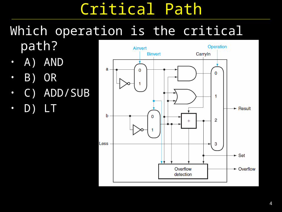
Critical PathWhich operation is the critical path?• A) AND• B) OR• C) ADD/SUB• D) LT

5
Critical PathWhat is the length of the critical path (in gates)?• A) 3• B) 5• C) 8• D) 11
6
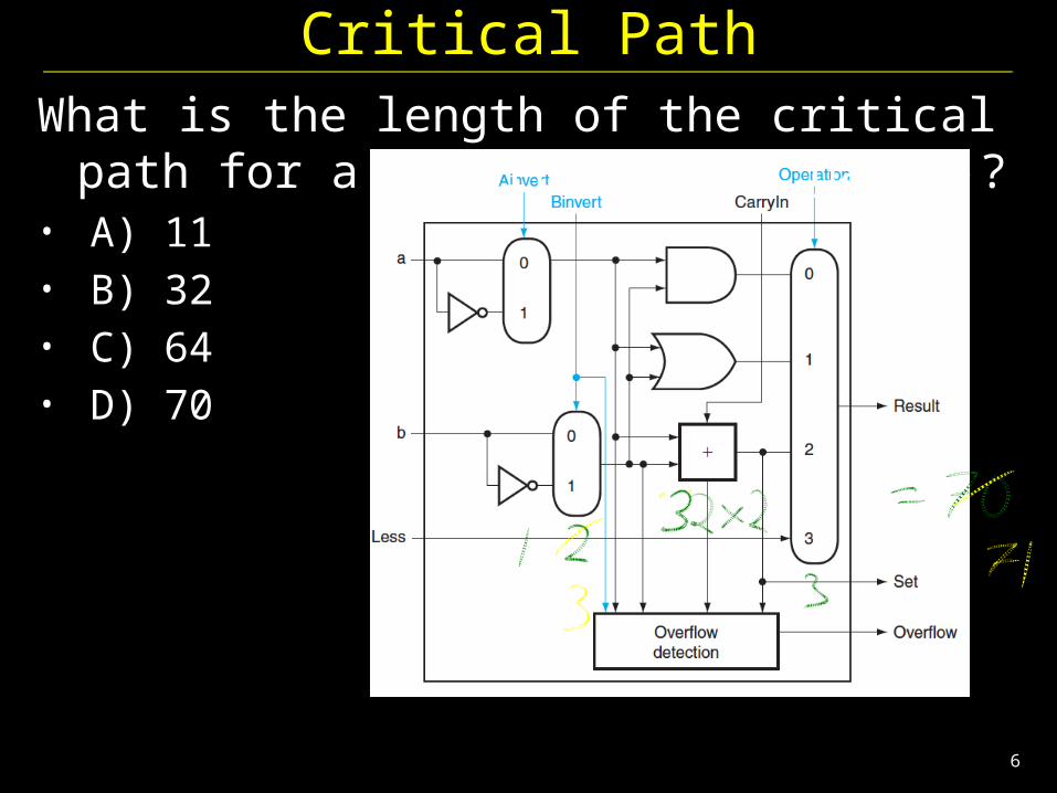
Critical PathWhat is the length of the critical path for a 32-bit
ALU (in gates)?• A) 11• B) 32• C) 64• D) 70
7
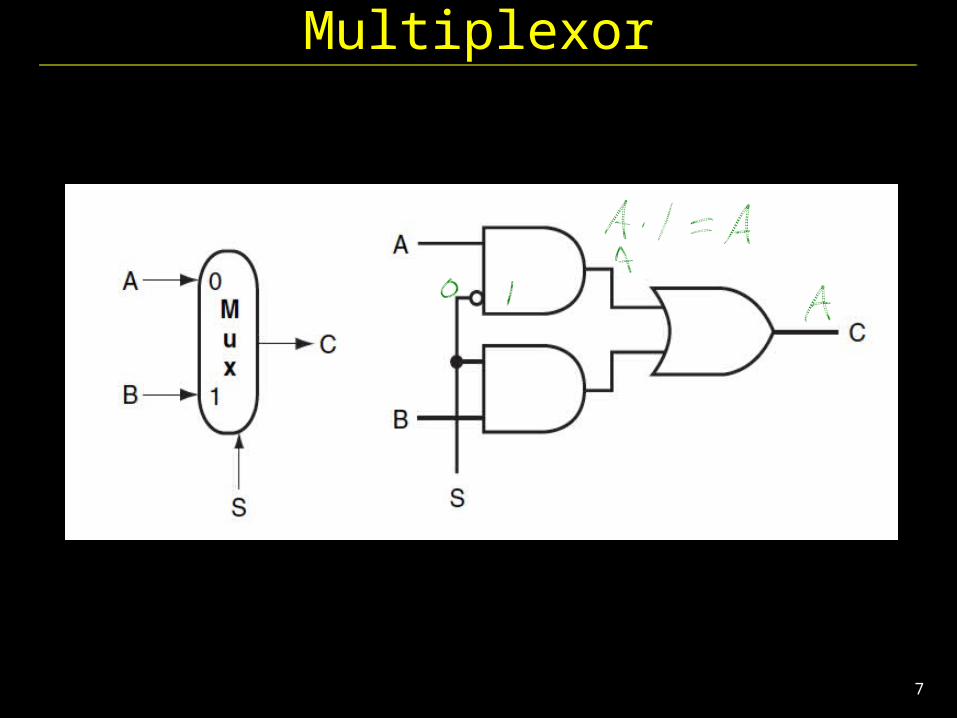
Multiplexor

8
Multiplexor

9
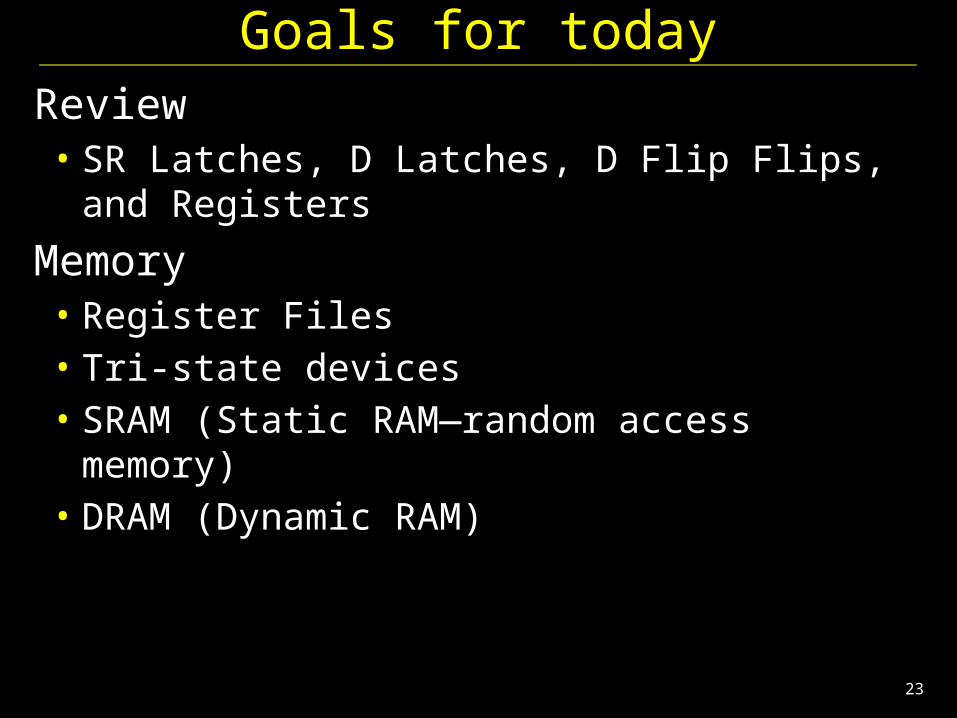
Goals for todayReview• SR Latches, D Latches, D Flip Flips, and Registers
Memory• Register Files• Tri-state devices• SRAM (Static RAM—random access memory)• DRAM (Dynamic RAM)
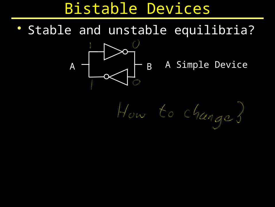
Bistable Devices
A B A Simple Device
• Stable and unstable equilibria?

Bistable Devices
• In stable state, A = B
• How do we change the state?
A B
A B
1
A B
10 0
A Simple Device
• Stable and unstable equilibria?

12
SR Latch
S
R
Q
Q
13
SR Latch
S R Q Q
0 0
0 1
1 0
1 1
S
RQ
Q
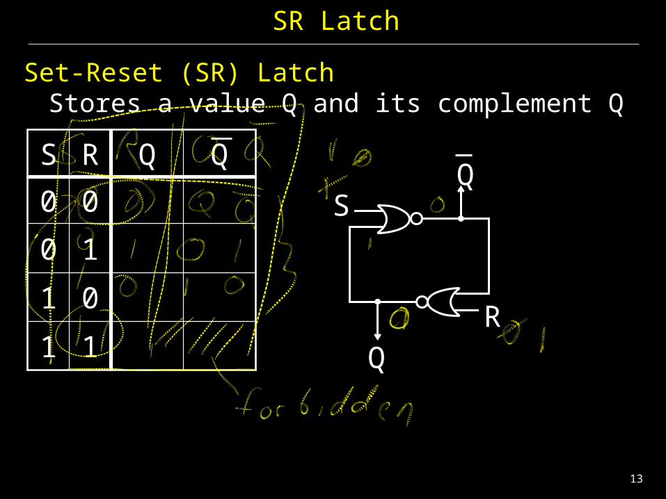
Set-Reset (SR) LatchStores a value Q and its complement Q

14
SR Latch
Set-Reset (SR) LatchStores a value Q and its complement Q
S R Q Q
0 0 Q Q
0 1 0 1
1 0 1 0
1 1 forbidden
S
R
Q
Q
S
RQ
Q
15
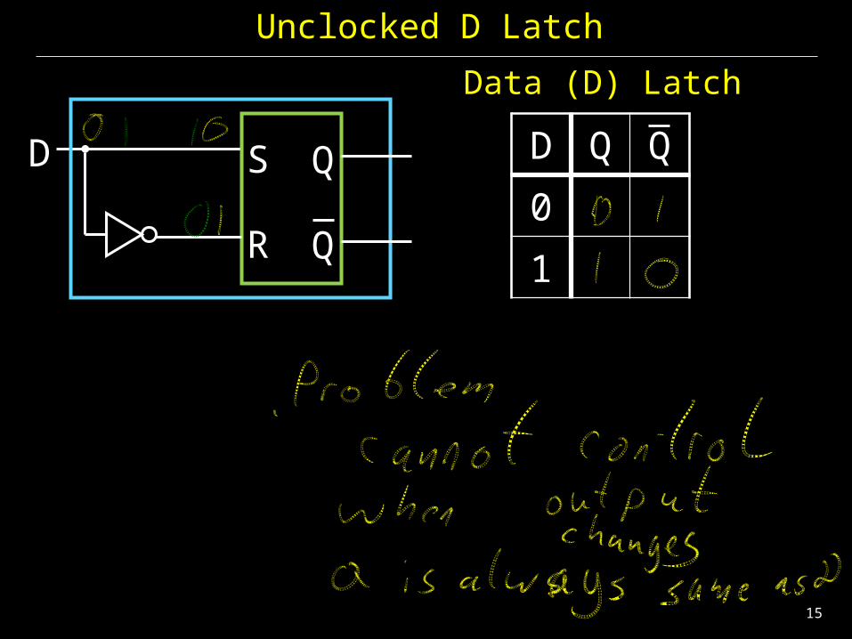
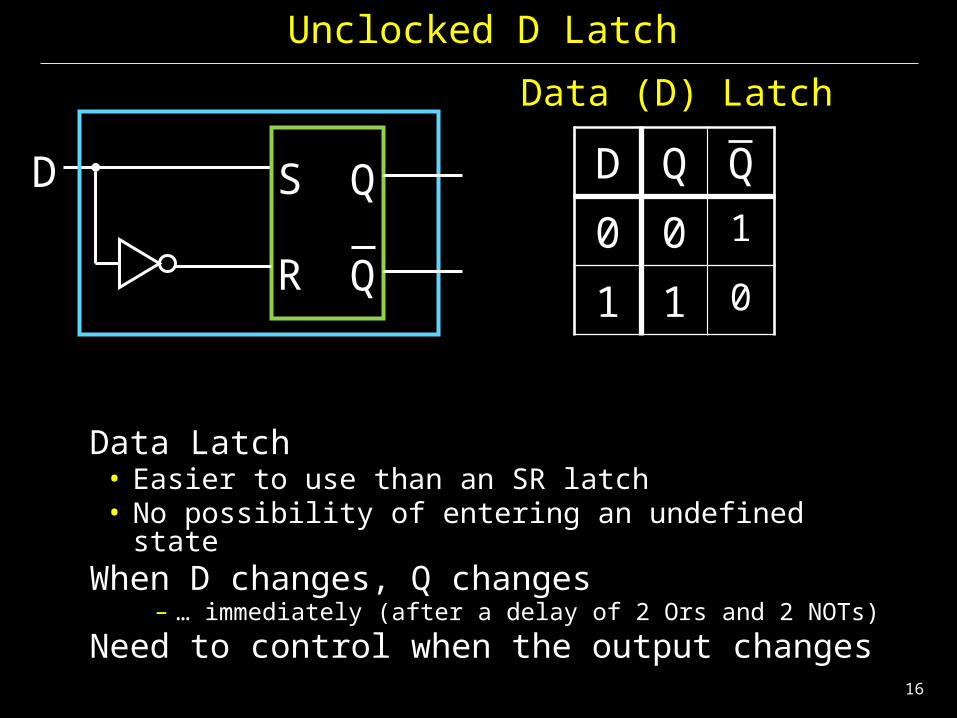
Unclocked D Latch
Data (D) Latch
D Q Q
0
1
S
R
D Q
Q
16
Unclocked D Latch
Data (D) Latch
D Q Q
0 0 1
1 1 0
S
R
D Q
Q
Data Latch• Easier to use than an SR latch• No possibility of entering an undefined state
When D changes, Q changes– … immediately (after a delay of 2 Ors and 2 NOTs)
Need to control when the output changes

17
D Latch with Clock
S
R
D
clk
Q
Q
Level Sensitive D LatchClock high: set/reset (according to D)Clock low: keep state (ignore D)
D Q Q
0 0 1
1 1 0

18
D Latch with Clock
S
R
D
clk
Q
Q
S R Q Q
0 0 Q Q
0 1 0 1
1 0 1 0
1 1 forbidden
D Q Q
0 0 1
1 1 0
clk D Q Q
0 0 Q Q
0 1 Q Q
1 0 0 1
1 1 1 0

19
D Latch with Clock
S
R
D
clk
Q
Q
D Q Q
0 0 1
1 1 0
clk D Q Q
0 0 Q Q
0 1 Q Q
1 0 0 1
1 1 1 0
clk
DQ
20
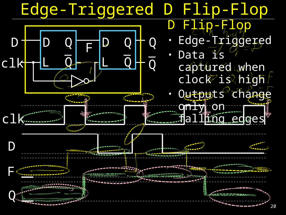
Edge-Triggered D Flip-FlopD Flip-Flop• Edge-Triggered • Data is captured
when clock is high• Outputs change only
on falling edges
D Q
Q
D Q
Qc
FL L
clk
D
F
Q
c
Q
Q
D
clk

21
RegistersRegister• D flip-flops in parallel • shared clock• extra clocked inputs:
write_enable, reset, …
clk
D0
D3
D1
D2
4 44-bitreg

22
Voting Machine
mux
32
...reg
dete
ct
enc
3
decoder (3-to-8)
32 32
32
LED
dec
3
E
+1
regE
regE
regE
mux
23
Goals for todayReview• SR Latches, D Latches, D Flip Flips, and Registers
Memory• Register Files• Tri-state devices• SRAM (Static RAM—random access memory)• DRAM (Dynamic RAM)
24
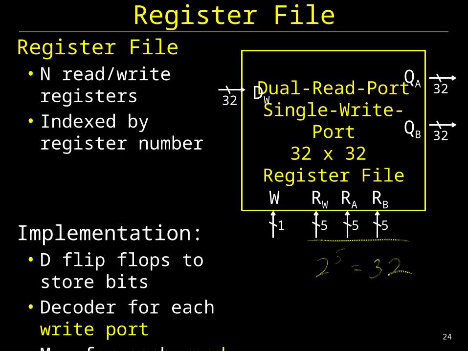
Register FileRegister File• N read/write registers• Indexed by
register number
Implementation:• D flip flops to store bits• Decoder for each write port• Mux for each read port
Dual-Read-PortSingle-Write-Port
32 x 32 Register File
QA
QB
DW
RW RA RBW
32
32
32
1 5 5 5

25
Register FileRegister File• N read/write registers• Indexed by
register number
Implementation:• D flip flops to store bits• Decoder for each write port• Mux for each read port
Dual-Read-PortSingle-Write-Port
32 x 32 Register File
QA
QB
DW
RW RA RBW
32
32
32
1 5 5 5

26
Register FileRegister File• N read/write registers• Indexed by
register number
Implementation:• D flip flops to store bits• Decoder for each write port• Mux for each read port
Dual-Read-PortSingle-Write-Port
32 x 32 Register File
QA
QB
DW
RW RA RBW
32
32
32
1 5 5 5

27
TradeoffsRegister File tradeoffs
+ Very fast (a few gate delays for both read and write)+ Adding extra ports is straightforward– Doesn’t scale
28
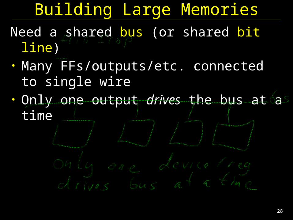
Building Large MemoriesNeed a shared bus (or shared bit line)• Many FFs/outputs/etc. connected to single wire• Only one output drives the bus at a time

29
Tri-State Devices
DQ
E E Vdd
Gnd
E D Q0 0 z
0 1 z
1 0 0
1 1 1
D QD
Tri-State Buffers

30
Tri-State Devices
DQ
E E Vdd
Gnd
E D Q0 0 z
0 1 z
1 0 0
1 1 1
D QD
Tri-State Buffers

31
Shared BusS0D0
shared line
S1D1 S2D2 S3D3 S1023D1023
32
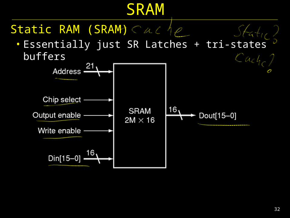
SRAMStatic RAM (SRAM)• Essentially just SR Latches + tri-states buffers

33
SRAM Chip

34
SRAM Chip
row
dec
oder
A21-10 column selector, sense amp, and I/O circuitsA9-0
CSR/W
Shared Data Bus
35
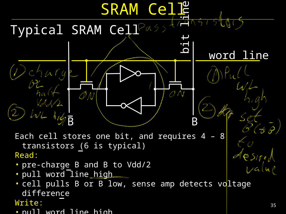
SRAM CellTypical SRAM Cell
BB
word linebit l
ine
Each cell stores one bit, and requires 4 – 8 transistors (6 is typical)Read:• pre-charge B and B to Vdd/2• pull word line high• cell pulls B or B low, sense amp detects voltage differenceWrite:• pull word line high• drive B and B to flip cell

36
SRAM Modules and Arrays
A21-0
Bank 2
Bank 3
Bank 4
1M x 4SRAM
1M x 4SRAM
1M x 4SRAM
1M x 4SRAM
R/W
msb lsb
CS
CS
CS
CS
37
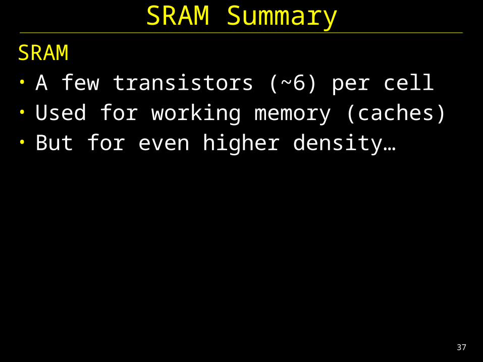
SRAM• A few transistors (~6) per cell• Used for working memory (caches)• But for even higher density…
SRAM Summary
38
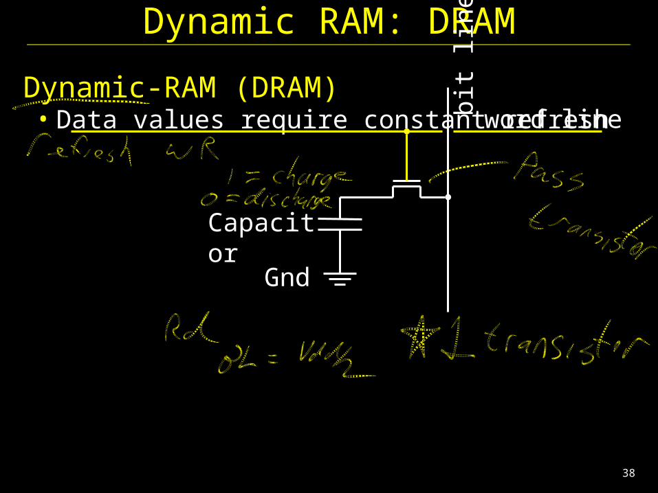
Dynamic RAM: DRAM
Dynamic-RAM (DRAM)• Data values require constant refresh
Gnd
word linebit l
ine
Capacitor

39
Single transistor vs. many gates• Denser, cheaper ($30/1GB vs. $30/2MB)• But more complicated, and has analog sensing
Also needs refresh• Read and write back…• …every few milliseconds• Organized in 2D grid, so can do rows at a time• Chip can do refresh internally
Hence… slower and energy inefficient
DRAM vs. SRAM
40
MemoryRegister File tradeoffs
+ Very fast (a few gate delays for both read and write)+ Adding extra ports is straightforward– Expensive, doesn’t scale– Volatile
Volatile Memory alternatives: SRAM, DRAM, …– Slower+ Cheaper, and scales well– Volatile
Non-Volatile Memory (NV-RAM): Flash, EEPROM, …+ Scales well– Limited lifetime; degrades after 100000 to 1M writes
41
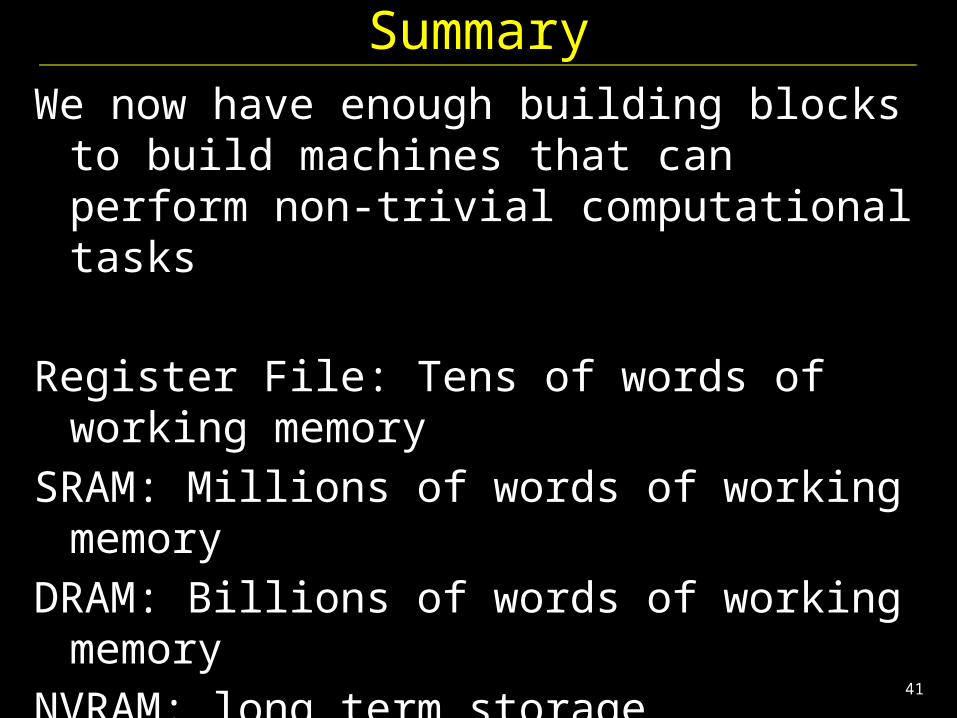
SummaryWe now have enough building blocks to build
machines that can perform non-trivial computational tasks
Register File: Tens of words of working memorySRAM: Millions of words of working memoryDRAM: Billions of words of working memoryNVRAM: long term storage
(usb fob, solid state disks, BIOS, …)

![Hakim Weatherspoon CS 3410 · 2020-01-08 · Calling Conventions Hakim Weatherspoon CS 3410. Computer Science. Cornell University [Weatherspoon, Bala, Bracy, McKee and Sirer]](https://static.fdocuments.us/doc/165x107/5f96a8e542e1ef67bd47302f/hakim-weatherspoon-cs-2020-01-08-calling-conventions-hakim-weatherspoon-cs-3410.jpg)


![Assemblers, Linkers, and Loaders€¦ · Assemblers, Linkers, and Loaders [Weatherspoon, Bala, Bracy, and Sirer] Hakim Weatherspoon. CS 3410. Computer Science. Cornell University](https://static.fdocuments.us/doc/165x107/5f86a2d8bd4b266b2809b708/assemblers-linkers-and-loaders-assemblers-linkers-and-loaders-weatherspoon.jpg)

