Power Integrity and Ground Bounce Simulation of High Speed PCBs

1
Abstract- This paper is concerned with the analysis and opti-mization of the gr ound bounce in digital CMOS circuits.First, an analytical method for calculating the gr ound bounceis pr esented. The proposed method relies on accurate modelsof the short-channel MOS device and the chip-package inter-face par asitics. Next the effect of gr ound bounce on the prop-agation delay and the optimum taper ing factor of a multi-stage buffer is discussed and a mathematical r elationship fortotal pr opagation delay in the pr esence of the ground bounceis obtained. Effect of an on-chip decoupling capacitor on theground bounce wavefor m and circuit speed is analyzed nextand a closed for m expr ession for the peak value of the differ-ential-mode component of the ground bounce in terms of theon-chip decoupling capacitor is pr ovided. Finally a designmethodology for controlling the switching times of the outputdr iver s to minimize the gr ound bounce is pr esented.
Index Terms Signal integr ity, Noise, Ground bounce,Taper ed buffer , On-chip decoupling capacitor , Skew control.
I. INTRODUCTION
Signal integrity is a crucial problem in VLSI circuits and isbecoming increasingly important as the minimum feature size ofdevices shrinks to 130 nanometers and below. A major compo-nent of the circuit noise is the inductive noise. In fact, fasterclock speeds and larger number of devices and I/O drivers as dic-tated by Moore’s Law (and therefore larger value of total circuitcurrent) have resulted in increased amount of this type of noise in
the power and ground planes (i.e., the noise, also known as
the power/ground bounce). It is a critical and challenging designtask to control the amount of inductive noise that is inserted intothe power planes.
Package pins, bonding wires, and on-chip IC interconnectsall have parasitic inductances. When an inductor current experi-ences time-domain variation, a voltage fluctuation is generatedacross the inductor. This voltage is proportional to the inductanceof the chip-package interface and the rate of change of the cur-rent. As a result, when the logic cells in a circuit are switched onand off, the voltage levels at the power distribution lines of thecircuit fluctuate. This inductive noise is sometimes referred to asthe simultaneous switching noise because it is most pronouncedwhen a large number of I/O drivers switch simultaneously.
To quantify the magnitude of the inductive noise and itseffect on the circuit performance by way of an example, assumethat the effective inductance between the ground of the chip andthe ground of the Printed-Wiring Board (PWB) plane is 10nH,and the rate of change of the switching current is 5 mA/nsec perI/O pin (c.f. Fig. 1). Assuming that 16 drivers switch at the sametime (to provide data for a 16-bit bus), the peak value of theground bounce is about 0.8V, which is quite large in the contextof today’s operating voltage levels and can therefore cause harm-ful effects on the circuit, such as false switching in the logicgates, especially in dynamic logic gates, timing failure, and tim-ing jitter in the on-chip clock generators.
Fig. 1. A simplified circuit schematic of 16 output buffers switch-ing simultaneously.
Due to the large slew rates of the currents flowing throughthe bond wires and package pins, the ground and supply voltageseen by the output drivers experience bouncing due to the para-sitics associated with the package and connections to the chip.Fluctuations on the supply and ground rails are further increasedwhen output drivers switch simultaneously. A number ofresearchers have studied the power and ground (P/G) bounceproblem. The P/G bounce noise is the switching noise on thepower-supply and ground lines which consists of the resistive IRdrop due to bond wire and trace resistances, inductive -noisedue to the chip-package interface inductance including bond wireself-inductance, trace self inductance, trace-to-trace mutualinductance, and capacitive coupling due to the chip-packageinterface cross-coupling capacitances. While, due to circuit inno-vations and device scaling, the speed and accuracy of integratedcircuits have steadily increased, the performance of packages,especially for low-cost applications, has not significantlyimproved. This trend follows from the rather poor scalablility ofpackaging technology and the design environments in whichthese packages are being employed.
dIdt-----
P. Heydari is with the Department of Electrical and Computer Engineering, Uni-versity of California, Irvine, CA 92697-2625 USA.M. Pedram is with the Department of Electrical Engineering Systems, University of Southern California, Los Angeles, CA 90089 USA.
.
.....
L = 10 nH
mA/nsecI∆t∆
----- 5=
.
.. ...
VDD
1
2
16
Out1
Out2
Out16
CL1
CL2
CL16
NLI∆t∆
----- 0.8V=
I∆
Ground Bounce in Digital VLSI Circuits
Payam Heydari, Member, IEEE, Massoud Pedram, Fellow, IEEE

2
In the past a number of approaches have been proposed toanalyze the power/ground bounce and its effect on the perfor-mance of VLSI circuits. In [1], Senthinathan et al. described anaccurate technique for estimating the peak ground bounce noiseby observing a negative local feedback that is actually present inthe current path of the driver. The work, however, suffers from anunrealistic assumption about the time-domain variations of theswitching current waveform. More specifically, paper [1]assumes that the switching currents of output drivers have a tri-angular wave-shapes. In [2], Vaidyanath et al. relax this assump-tion by deriving an expression for peak value of ground bouncevalue under the more realistic and milder assumption that theground bounce is a linear function of time during the output tran-sition of the driver. The authors do not obtain time domain wave-form of the ground bounce and use a simplistic model of the pad-pin parasitics (i.e., inductance only).
More recently a number of researchers have tried to considerthe short channel effects of MOS devices on the ground bouncewaveform [3][4][5]. While most prior works were concentratedon the case where all the drivers switch simultaneously, paper [4]considers the more realistic case where the drivers may switch atdifferent times. The idea of considering the effects of groundbounce on the tapered buffer has been presented in a paper byVemuru [6]. The author, however, does not provide the quantita-tive analysis required for designing the optimum number of driv-ers in the tapered buffer chain. In [7], Vittal et al. describe analgorithm based on integer linear programming to skew theswitching time of the drivers to minimize the ground bounce.However, since the ground bounce is analyzed by a high-levelapproach and does not utilize the characteristics of the groundbounce waveform, the proposed technique is far from beingaccurate. In addition, it increases the propagation delay throughthe output buffers.
This paper is devoted to the analysis and optimization of theground bounce. We use a simple, yet accurate, circuit to modelthe chip-package interface parasitics. The ground bounce isaddressed with no assumptions about the form of the switchingcurrent or noise voltage waveforms. Throughout this paper, themain focus will be on the ground bounce noise. However, thesame approach can also be used for power-supply noise analysis.We circumvent the drawbacks of previous approaches by adopt-ing a more accurate chip-package interface model consisting ofresistive, and inductive components. Next, the effect of groundbounce on the tapered buffer design is considered, and a mathe-
matical approach is adopted to consider the ground bounce effecton the propagation delay and the optimal tapering factor. We nextaddress the impact of an on-chip decoupling capacitor on thepeak value of the ground bounce. This is an important problemsince the decoupling capacitors are widely used to control theground bounce and to reduce the resonant frequency of the powerand ground network [8][9][10]. We thus present a method to finda closed-form expression for the peak value of the differential-mode component of the ground bounce as a function of thedecoupling capacitor. We also propose a technique to skew theoutput buffers. By this method the peak amplitude of the groundbounce is reduced to at least 65% of its value when all the driversswitch simultaneously. Our technique does not introduce a largedelay after skewing the switching times of buffers.
II. CIRCUIT MODELING
In this section a simplified circuit model for the chip-packageinterface parasitics based on the layout schematic of the outputpad drivers, the bond wires, and package pins is presented. Wealso discuss how to analyze the ground bounce in the generalcase of several off-chip drivers switching as the same time.
A. Modeling the chip-package interface parasitics
Fig. 2 depicts the layout schematic of three identical outputpad drivers along with bond wires and package pins.
Fig. 2. A layout schematic for the output drivers along with thebonding wires, pads and package pins.
VDD
GND
Vin
tr
VDD
Q1
Q2
LbRb
Vin:rv
Rv Rv
RG RG
rG
CL
Rp Lp
VDD
Cp Cb
Fig. 3. The circuit representation of Fig. 2
Cp Cb
Vin Q5
Q6
rv
rG
CL
Cp Cb
LbRbRp Lp
Cp Cb
Vin Q3
Q4
rv
rG
CL
LbRbRp Lp
Cp Cb
Chip GND
PWB GND
LGLG
CG CG
Lv Lv
CvCv
LbRbRp Lp LbRbRp Lp

3
In general, there are two major inductive components whichcontribute to the total ground bounce: the inductive noise due tothe on-chip interconnect, and the inductive noise due to the chip-package interface consisting of bond wire self-inductance, traceand pin self-inductances, and trace-to-trace mutual inductance.
Shown in Fig. 3 is the electrical model of Fig. 2. The on-chippower/ground wires are modeled as a single RLC circuit(RG,LG,CG) for the on-chip ground wire and a single RLC circuit(Rv,Lv,Cv) for the on-chip power-supply wire. The off-chip driv-ers are normally placed in a close proximity to the pads and bondwires. Therefore the on-chip ground and power lines exhibitsmall electrical parasitics and thus the two representative RLCcircuits for on-chip power and ground wires, (Rv,Lv,Cv) and(RG,LG,CG), are very small compared to the chip-package inter-face parasitics and can thus be ignored. Bond wires, and packagetraces and pins are modeled using two separate RLC circuitsdenoted by (Rb,Lb,Cb) and (Rp,Lp,Cp), respectively, as depicted inFig. 3.
There are two RLC circuits in series that are on the path fromthe chip ground to the PWB ground. Table I lists the typical chip-package interface parasitics for the CPGA, PPGA, H-PBGA, andTQFP packages [11] [12]. The values listed assume that the pack-age is mounted on the mother-board using a socket, so the pin/land parasitics include the socket effects as well as connectingvia parasitics inside the package.
Based on practical values specified in Table I, the circuitmodel can be simplified to a series RL circuit because the magni-tude response of the capacitive reactance at today’s target clockfrequencies is more than ten times larger than that of the equiva-lent impedance of the series RL circuit. The ground wiring con-nection of Fig. 3 is thus simplified to the circuit shown in Fig. 4where all the ground and power wires reach a single point. Theupcoming ground bounce analysis will be performed on the cir-cuit shown in Fig. 4 where N output drivers driving off-chipcapacitive loads. According to this figure, R and L represent theground and power chip-package interface parasitics while Rw andLw represent the load terminal parasitics. tr is the rise-time of theinput waveform and T is the cycle time.
Another design aspect which should be considered whenanalyzing the ground bounce is that the output pad driver has alarge dimension because it should drive a large capacitor. To esti-mate the range of transistor sizes used in output buffers, assumethat there is a single CMOS driver driving a 50 pF off-chipcapacitor. Also assume that the off-chip operating frequency isaround 200MHz. A simple calculation reveals that in order tocharge up this capacitor to the supply voltage of 2.5V in less than20% of the total clock period, the required current is 125mA. Thedevice parameters provided by MOSIS for a 0.25µm NMOS
device is: , µn,0 = 320 cm2/V.sec, and VTH0=0.4V.Using square-law MOS model the W/L ratio is approximately290, which for a minimum channel-length transistor gives rise toa channel width of 73µm. The large current drive requirement forthe off-chip CMOS drivers often demands the use of taperedbuffer chains.
Fig. 4. Circuit schematic of N output pad drivers.
B. Multiple output drivers
Ground bounce can become very large when multiple outputdrivers switch simultaneously. In this case the ground bounceequation is first calculated for a single driver. To account for theswitching effects of multiple output drivers, the NMOS (PMOS)gain parameter, βn(p) is modified as the summation of gainparameters of transistors in individual switching drivers. How-ever, in reality, not all the drivers switch exactly at the same time.Similar to [5], we assume that N output drivers switch simulta-neously while the remaining M drivers are quiet. The circuit rep-resentation of the problem is depicted in Fig. 5 (a). To considerthe effect of inactive drivers, assume that the gate terminals ofquiet drivers are at logic level “ HIGH”, which causes the NMOStransistors to be in the linear region and the PMOS transistors tobe in the cutoff region. The output terminals of the quiet driversare at logic level “LOW” . Unfortunately, the outputs of quietdrivers are exposed to the coupled noise coming from the supplyand ground rails. Shown in Fig. 5 (b) is the circuit of Fig. 5 (a)while the NMOS transistors of quiet drivers are modeled approx-imately by their drain-source resistances. The AC ground nodesof rDS resistors experience the coupled fluctuations from groundand supply lines as also depicted in Fig. 4 (b). As a result, theamount of current flowing through the quiet NMOS transistors
TABLE ISUMMARY OF PACKAGE I/O LEAD ELECTRICAL PARASITICS
FOR DIFFERENT PACKAGES
Electr ical Par ameter sWire-bonding Package Type
CPGA PPGA H-PBGA TQFP
Bond wire/die bump Rb (mΩ) 126-165 136-188 114-158 70-150
Bond wire/die bump Lb (nH) 2.3-4.1 2.5-4.6 2.1-4.1 1-4
Bond wire/die bump Cb (pF) 0.2-0.5 0.1-0.3 0.2-0.6 0.1-0.3
Pin/Land Rp (mΩ) 20 20 0 90-97
Pin/Land Lp (nH) 4.5-7.0 4.5-7.0 4.0-6.0 3-5
Pin/Land Cp (pF) 0.1 0.1 0.02 0.1-0.3
tox 58A°=
VDD
LR
Vin,1 Vout,1 Vout,N
....
L R
Vin,N
CL
tr
VDD
0
L, R: Equivalent inductance and resistance
Chip Gnd
PWB Gnd
of the bonding wire package planeand pin parasitics (chip-package interface)
CL
....LwRw LwRw

4
will be negligible, i.e., quiet drivers do not affect the groundbounce analysis. As mentioned earlier, the contribution of the Nswitching drivers on the ground bounce is taken into account bycalculating the ground bounce due to the switching action of asingle buffer and then modifying the device gain parameter, βn(p).
III. OFF-CHIP GROUND BOUNCE ANALYSIS
Consider an off-chip buffer driving a large capacitive load, asdepicted in Fig. 6. The chip-package interface parasitics are mod-eled using series RL circuits for ground, power and signal paths.Our goal is to obtain the ground bounce through a detailed circuitanalysis. This approach is easily extended to include a more gen-eral case in which several buffers switch simultaneously.
Fig. 6. An output driver driving CL . The series RL circuits modelthe chip-package interface parasitics
Since the input waveform is comprised of two differentshapes, a ramp voltage and a flat voltage part, and since theNMOS and PMOS devices operate in different regions of opera-tions during the transition from one input state to another, in whatfollows, the ground bounce for each of these two input shapes isanalyzed separately. Notice that a similar analysis may be per-formed for the power-supply bounce during the low-to-high out-put transitions. During the ground bounce analysis, only theeffect of NMOS current on the ground bounce is considered i.e.,
the effect of PMOS currents is ignored [3], [6]. Fig. 7 demon-strates the input, output, and ground bounce waveform in a cir-cuit consisting of a large off-chip inverter implemented in0.25µm CMOS process and a 4pF capacitive load.
Fig. 7. Ground bounce from HSPICE simulation results of a0.25µm CMOS process and classification of regions in groundbounce analysis
The chip-package interface parasitics for ground, supply, andsignal lines are modeled by series RL circuits whose values areindicated in Fig. 7. The NMOS transistor is off so long asvgs<Vtn. As vgs exceeds the threshold voltage, the NMOS transis-tor first enters its saturation region. The transistor stays in satura-tion region during the entire low-to-high input transition becausethe off-chip driver drives large capacitive loads, and as a result,the driver output slowly decreases from a logic high to a logiclow. As the output voltage decreases, so does the drain-sourcevoltage of the NMOS transistor. Eventually at t = ts (ts > tr) theNMOS transistor makes a transition from saturation region to lin-ear region. The NMOS transistor will stay in the linear region for
, until the next edge transition. This particular form ofdevice operating-mode transition in the presence of large capaci-tive loads allows one to utilize the BSIM3 MOS model withsome simplifications as detailed next.
According to the BSIM3 model for the short-channel NMOStransistor [8], the NMOS I-V equations for the saturation and lin-ear regions are as follows:
VDD
Vin
vn
….
….
….
….
VDD VDD
N M
VDD
Vin
vn
….
….
….
….
VDD VDD
N M
Fig. 5. N output drivers switch simultaneously and the remain-ing M drivers are quiet. (a) the actual circuit. (b) the simplifiedcircuit.
VDD
LR
Vin,1
Vout,1 Vout,N
....
L R
Vin,N
CL
tr
VDD
0
CL
....LwRw LwRw ....rDS,1 rDS,M
N M
(a)
(b)
Vin,1 Vout,1
tr
VDD
0CL
LwRw
VDDL R
LR
Symbol WaveD0:A0:v(in)
D0:A0:v(output)D0:A0:v(chp_gnd)
Volta
ges (
lin)
-500m
0
500m
1
1.5
2
2.5
Time (lin) (TIME)10n 12n 14n
Time=9.55e-09
2.5
2.09
0.561
An offichip driver driving a 4pF load capacitor
Vol
tage I
I I
I IIIV
Input : purple Output: red Ground_bounce: blue
L = 7nH, R = 0.6, CL=4pF
Region I: 0 tVtn
VDD--------- tr≤ ≤
Region II: Vtn
VDD
--------- tr t tr≤ ≤
Region III: tr t ts≤ ≤
Region IV: t ts≥
t ts>

5
(1)
where . From the aforementioned
discussion, the NMOS transistor will enter the linear region whenthe input voltage is VDD due to the presence of large off-chipcapacitive loads. The overdrive voltage is thus constant at VDD -Vtn. As a result, the nonlinear relationship between the saturateddrift velocity, νd,sat, and the drain-source saturation voltage,VDS,sat, is evaluated at . This leads to the following sim-plified transistor equation that holds true for the output drivers:
(2)
where
and
To account for the voltage variation of the source node, aconstant modifying factor, γ, varying between 0.7-0.9 is added tothe formulation. In this paper we assume that γ=0.8.
A similar current-voltage relationship can be derived for thePMOS transistor. Running several experiments and comparingthe results with the HSPICE simulation reveals that this simplifi-cation causes at most 2% error.
To obtain a better estimate for the ground bounce waveform,we distinguish between four different sub-intervals. Ourapproach is to derive the closed-form expressions for the groundbounce at each of these sub-intervals by solving the characteristicordinary differential equation (ODE) coming out of the circuitanalysis. We omit the details of how the differential equations aresolved and only provide the final expressions.
A. Ramp input
During the low-to-high input transition the NMOS transistorof the output driver experiences multiple region transitions.Unlike what is commonly assumed, the ground bounce is notzero for . Therefore we need to decompose theinterval [0 , tr] into two subintervals and obtain the groundbounce waveform for each of these regions.
1) Region I ( ):
During this interval, the NMOS transistor operates in itsweak-inversion region. When the transistor is operating in itsweak inversion region the amount of drain current flowingthrough the drain path is very small. Instead there is another cur-rent path from input to the ground network provided by the gate-
to-bulk capacitance Cgb of the transistor. Remember that in weakinversion, because the inversion layer contains littlecharge. However, Cgs can be thought as the series combination ofthe oxide and depletion capacitors [13], Therefore,
where Cox is the parallel plate gate-to-channel capacitor, and Cjsis the depletion-region capacitor. Writing a KVL for the signalpath consisting of the input source, capacitor Cgb, and the seriesRL circuit leads to the following ODE:
(3)
(4)
where , , , .
2) Region II ( ):
If the overdrive voltage is larger than the NMOS thresholdvoltage, Vtn, the NMOS transistor turns on and operates in its sat-uration region. The off-chip driver’s drain current flowingthrough the chip-package interface parasitics will generate theground bounce, vn. Utilizing the characteristic I-V equation of asaturated NMOS transistor (Eq. (2)) and writing a simple KVLfor the drain current path consisting of NMOS transistor and theRL circuit in the circuit shown in Fig. 6, leads us to the followingODE:
(5)
where and .
Solving the above ODE for vn yields the following expres-sion for the ground bounce in the interval interms of t:
(6)
where:
, , , .
and with the following initial condition:
Note that Eq. (4) is a monotonically increasing function oftime. Therefore, the peak value of the voltage vn(t) occurs at theend of this operating region when t = tr . For the input set-tles at VDD and the ground bounce amplitude decreases. This
ID
WυsatCoxW VGS Vtn VDS sat,–– )( VDS VDS sat,≥
µnCoxWL----- 1
1VDS
LEsat-------------+
---------------------- VGS VtnVDS
2---------–– VDS VDS VDS sat,≤
=
VDS sat,LEsat VGS Vtn–( )LEsat VGS Vtn–+------------------------------------------=
VGS VDD=
ID
βn VGS Vtn– )( VDS VDS sat,≥
12--- µnCox
WL----- VDD Vtn)–( VDS VDS VDS sat,≤
=
βn0.5µnCox W L⁄( )
1VDD Vtn–----------------------- γ
LEsat-------------+
-------------------------------------------=
VDSsat,LEsat VGS Vtn–( )
LEsat γ VDD Vtn–( )+--------------------------------------------------=
0 Vtn VDD )⁄( tr ],[
0 tVtn
VDD---------tr≤ ≤
Cgs Cgd= 0≈
Cgs Cgb Cgd+ + Cgb≈ WLCox Cj s
Cox Cj s+---------------------- =
d2vn
dt2---------- R
L---( )dvn
dt--------
vn
LCgb------------++ R
L--- VDD
tr
----------= 0 tVtn
VDD
---------- tr≤ ≤
vn t( )VDD
trωd
--------------eα t– ωd tsin 2α VDD
trωn2
--------------
1ωn
ωd------e
α t– ωdt θ+( )sin–+=
α R2L------= ωn
2 1LCgb------------= ωd ωn
2 α2–= θ ωd
α------tan
1–=
Vtn
VDD----------tr t tr≤ ≤
τd
dvnR 1
βn-----+
L---------------------vn+
VDD
tr---------- R
L---Vtn– R
L---
VDD
tr----------τ+= 0 τ τr≤ ≤
τ tVtn
VDD---------- tr–= τr 1
Vtn
VDD----------– tr=
Vtn VDD )⁄( tr t tr≤ ≤
vn t( ) vn t0( )ep t t0–( )– Us
p------ 1 e
p t t0–( )––( )+ u t t0–( )=
vn t( ) vn t0( )ep t t0–( )– Us
p------ 1 e
p t t0–( )––( )
Ur
p2------ p t t0–( ) 1 e
p t t0–( )––( )–[ ]+ + u t t0–( )=vn t( ) vn t0( )e
p t t0–( )– Us
p------ 1 e
p t t0–( )––( )
Ur
p2------ p t t0–( ) 1 e
p t t0–( )––( )–[ ]+ + u t t0–( )=vn t( ) vn t0( )e
p t t0–( )– Us
p------ 1 e
p t t0–( )––( )
Ur
p2------ p t t0–( ) 1 e
p t t0–( )––( )–[ ]+ + u t t0–( )= t0 t tr≤ ≤
pR
1βn-----+
L---------------------= Us
VDD
tr---------- R
L---Vtn–= Ur
RL---
VDD
tr----------= t0
Vtn
VDD----------tr=
vn 0( ) VDDtrωd--------------e α t– ωd tsin 2α VDD
trωn2
--------------
1ωnωd---------e α t– ωd t θ+( )sin–
tVtn
VDD-------------
tr=
+=
t tr>

6
means that vn(tr) is a global maximum for the ground bouncewaveform.
B. Constant input
For the input waveform reaches the supply voltageVDD. The rate of change of drain current flowing through theseries RL circuit decreases, which causes the ground bounce todecrease in time as well. The ground bounce analysis is per-formed on two distinct sub-intervals; when the NMOStransistor is still in the saturation region, and when the tran-sistor makes a transition to the linear operating region.
1) Region III ( ):
Over the time interval , the input is flat at VDD andthe NMOS transistor operates in the saturation. The correspond-ing ODE becomes:
(7)
with the following initial condition:
The ground bounce over this time interval is:
(8)
At t = ts the NMOS transistor experiences a transition in itsoperating mode and enters the linear region. The drain-sourcevoltage of NMOS transistor at is equal to the saturateddrain-source voltage, VDS,sat . The equivalent circuit at isdemonstrated in Fig. 8.
Fig. 8. The equivalent circuit of Fig. 6. at
ts is determined by solving the following KVL equationaround the loop:
(9)where ωc is the clock frequency in rad/sec, and vn(tr) is obtainedby evaluating (6) at . VDS,sat is given by Eq. (2) in which
.
2) Region IV ( ):
For , the NMOS transistor enters the linear region and ismodeled by a voltage dependent finite on-resistance rDS . Shownin Fig. 9, the equivalent circuit consisting of the load capacitor,
CL, the parasitic resistance and inductance, Rw and Lw, a voltagedependant resistance, rDS, and the chip-package interface equiva-lent parasitics, R and L, all in series, is solved to obtain theground bounce voltage.
Fig. 9. The equivalent circuit of Fig. 6. at
Note that during the design of the output drivers, their W/Lratio is assumed to be large enough so that they can provide suffi-cient current for the off-chip load. This implies that rDS values ofoff-chip drivers lie within the range of 20Ω-80Ω . In practice,
and the ground bounce experi-
ences a decaying oscillatory waveform over as alsoshown in Fig. 7. Since in each cycle of the oscillation the electricenergy across the load capacitor converts to the electromagneticenergy stored in the electromagnetic field across the inductor anddissipated energy in the resistor, we have a complete fluctuationaround the steady-state which is zero volt in this case and theground bounce passes through a minimum undershoot. The cur-rent i satisfies the following second-order ODE:
(10)
with the following initial conditions:
The solution to Eq. (10) is utilized to derive ground bounce volt-age vn(t) over the time interval :
(11)
where
, , ,
, .
Fig. 10 compares our analytical approach with the HSPICEsimulation for the three output drivers switching simultaneously
t tr>
tr t ts≤ ≤t ts≥
tr t ts≤ ≤tr t ts≤ ≤
td
dvnR
1βn-----+
L---------------------vn+
RL--- VDD Vtn–( )= tr t ts≤ ≤
vn tr–( ) vn tr
+( )=vn tr–( ) vn tr
+( )=
vn t( ) vn tr( )ep– t tr–( ) R
R 1 βn⁄+---------------------- VDD Vtn)–( 1 e
p– t tr–( )–
+ u t tr–( )= vn t( ) vn tr( )ep– t tr–( )
+ u t tr–( )=
tr t ts≤ ≤
t ts=t ts
–=
LwRw
CL
LRID βn VDD vn– Vtn– )(=
Vout
t ts–=
VDDβn
CL------ VDD Vtn–( )–VDD
βn
CL------ VDD Vtn–( ) ts tr–( )
βn
CL------ vn t( ) td
tr
ts1
Rw jωc Lw+R jωc L+
----------------------------+ vn ts( )––– VDS sat,≈1Rw jω cLw+R jω cL+
----------------------------+ vn ts( )– VDS sat,≈
1Rw jωcLw+R jω cL+
----------------------------+ vn ts( )– VDS sat,≈
t tr=VGS VDD vn ts( )–=
t ts>t ts>
LwRw
CL
LR
Vout
rDS i
vn(t)
t ts+
=
R Rw rDS
+ +( ) 2 L Lw+( ) CL⁄<ts T 2⁄,[ ]
d 2idt 2-------
Rw R rDS+ +L
------------------------------- didt----- 1
LCL----------i+ + 0= t ts≥
i ts( ) I βn VDD Vtn vn ts( ) )––(==
didt----- ts( ) I ′=
1 Rβn+( ) vn ts( ) Rβn VDD Vtn)–(–L
-----------------------------------------------------------------------------------=
t ts≥
vn t( ) Vc ωd′ t ts–( )cos Vs ωd
′sin t ts–( )+( )eα′ t ts–( )–
= t ts≥
α′ Rw rDS R+ +2 L Lw+( )
-------------------------------= ωn′ 2 1
L Lw+( )CL---------------------------= ωd
′2 ωn′2 α′ 2
–=
Vc RI LI ′+= VsRα′ Lωn
′2–ωd′
-------------------------- IR Lα′–
ωd′------------------ I
′+=Vs
Rα′ Lωn′2–
ωd′-------------------------- I R Lα′–
ωd′------------------
I ′+=

7
and with the chip-package interface parameter values specified inthe figure.
Clearly our analysis can follow the HSPICE simulation innsec. The undershoot time is predicted within 1%
error. The error in the transition between the exponential and thedecaying oscillatory case is due to the error in modeling the time-varying nonlinear voltage-controlled on-resistance of the MOSdevice.
IV. TAPERED BUFFER DESIGN FOR GROUND BOUNCE OPTIMIZATION
To drive large off-chip capacitances with a minimum ofpropagation delay, it is necessary to use an output buffer consist-ing of a number of CMOS inverters with gradually increasingdriving capability as also indicated in Fig. 11 [14]. The taperingfactor u is the ratio between the gate aspect ratios of two consec-utive inverters in the inverter chain.
Fig. 11. A CMOS buffer consisting of a series of inverters withgradually increasing driving capability. The chip-package inter-
face parasitics are modeled using series RL circuits.
The ground bounce causes an increase in the propagationdelay of the output buffer and thus affects the optimal scalingfactor in a series of tapered buffers [6]. As a result, the analyticalresults for the optimum scaling factor and the optimum numberof output drivers proposed in [14] and [15] are no longer validbecause they do not address the effects of non-ideal ground andpower lines. As a consequence, new formulas that account for thepower/ground noise effect on the tapered buffer design isrequired. From section III.A recall that the ground bounce isdependent on the nonzero input transition time of the driver.Hence, the first step is to derive the propagation delay of a singledriver having short-channel devices controlled by a real flattenedramp input and under the ideal ground condition (R, L=0).
Fig. 12 shows the result of the HSPICE simulation per-formed on a 0.25µm CMOS inverter. The device parameters aretaken from TSMC 0.25µ single-poly, five metal CMOS processprovided by MOSIS. The device characteristics are also specifiedin the figure.
Fig. 12. The input and output waveforms of an inverter simulatedby HSPICE. (W/L)n=5/0.25, (W/L)p=10/0.25 (in terms of µm),and CL=0.09pF.
0 0.5 1 1.5 2 2.5 3
x 10−9
−0.4
−0.2
0
0.2
0.4
0.6
0.8
1
Our simulation : −−
HSPICE:−
Time (sec)
Gro
un
d b
ou
nce
(vo
lts)
Ground bounce waveforms: L=2nH, W/L=100/0.25, CL=15pF, R=1ohm
Fig. 10. Ground bounce simulation. (dash): our simulation(plane): HSPICE.
0 t 0.5≤ ≤
.....
LR
LwRw
LRCL
VDD
Vout
W L⁄( )i
W L⁄( ) i 1–------------------------ u= ; for i = 1, ...., P
Symbol Wave
D0:A0:v(in)
D0:A0:v(out)V
olt
ag
es
(li
n)
0
200m
400m
600m
800m
1
1.2
1.4
1.6
1.8
2
2.2
2.4
2.6
Time (lin) (TIME)4.98n 5n 5.02n 5.04n 5.06n 5.08n 5.1n 5.12n 5.14n 5.16n 5.18n 5.2n
5.22n
The response of an inverter to a flattened ramp (CL=0.09pF)
NMOS: SaturationPMOS: Linear
NMOS: SaturationPMOS: Saturation
PMOS: Cutoff NMOS: Saturation
NMOS: LinearPMOS: Cutoff
I
I I
I I I
IV
tr / 2 tPHL
II I
I I I
IV
8
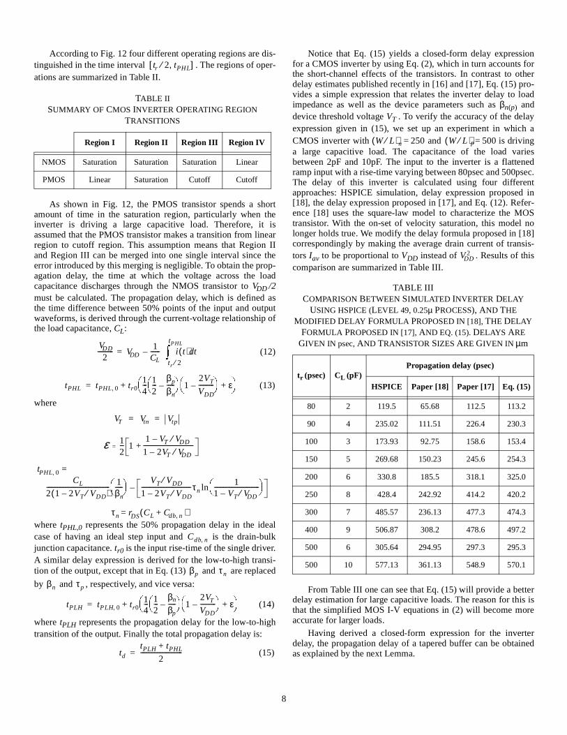
According to Fig. 12 four different operating regions are dis-tinguished in the time interval . The regions of oper-ations are summarized in Table II.
As shown in Fig. 12, the PMOS transistor spends a shortamount of time in the saturation region, particularly when theinverter is driving a large capacitive load. Therefore, it isassumed that the PMOS transistor makes a transition from linearregion to cutoff region. This assumption means that Region IIand Region III can be merged into one single interval since theerror introduced by this merging is negligible. To obtain the prop-agation delay, the time at which the voltage across the loadcapacitance discharges through the NMOS transistor to VDD /2must be calculated. The propagation delay, which is defined asthe time difference between 50% points of the input and outputwaveforms, is derived through the current-voltage relationship ofthe load capacitance, CL:
(12)
(13)
where
where tPHL,0 represents the 50% propagation delay in the idealcase of having an ideal step input and is the drain-bulkjunction capacitance. tr0 is the input rise-time of the single driver.A similar delay expression is derived for the low-to-high transi-tion of the output, except that in Eq. (13) and are replaced
by and , respectively, and vice versa:
(14)
where tPLH represents the propagation delay for the low-to-hightransition of the output. Finally the total propagation delay is:
(15)
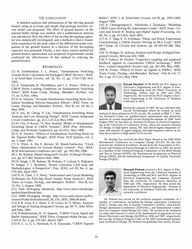
Notice that Eq. (15) yields a closed-form delay expressionfor a CMOS inverter by using Eq. (2), which in turn accounts forthe short-channel effects of the transistors. In contrast to otherdelay estimates published recently in [16] and [17], Eq. (15) pro-vides a simple expression that relates the inverter delay to loadimpedance as well as the device parameters such as βn(p) anddevice threshold voltage VT . To verify the accuracy of the delayexpression given in (15), we set up an experiment in which aCMOS inverter with and is drivinga large capacitive load. The capacitance of the load variesbetween 2pF and 10pF. The input to the inverter is a flattenedramp input with a rise-time varying between 80psec and 500psec.The delay of this inverter is calculated using four differentapproaches: HSPICE simulation, delay expression proposed in[18], the delay expression proposed in [17], and Eq. (12). Refer-ence [18] uses the square-law model to characterize the MOStransistor. With the on-set of velocity saturation, this model nolonger holds true. We modify the delay formula proposed in [18]correspondingly by making the average drain current of transis-tors Iav to be proportional to VDD instead of . Results of thiscomparison are summarized in Table III.
From Table III one can see that Eq. (15) will provide a betterdelay estimation for large capacitive loads. The reason for this isthat the simplified MOS I-V equations in (2) will become moreaccurate for larger loads.
Having derived a closed-form expression for the inverterdelay, the propagation delay of a tapered buffer can be obtainedas explained by the next Lemma.
TABLE IISUMMARY OF CMOS INVERTER OPERATING REGION
TRANSITIONS
Region I Region I I Region I I I Region I V
NMOS Saturation Saturation Saturation Linear
PMOS Linear Saturation Cutoff Cutoff
tr 2⁄ tPHL,[ ]
VDD
2---------- VDD
1CL------ i t( ) td
tr 2⁄
tPHL–=
tPHL tPHL 0, tr 0+14--- 1
2---
βp
βn
-----–
12VT
VDD
----------–
ε+
=
VT Vtn Vtp= =
ε 12--- 1
1 VT VDD⁄–
1 2VT VDD⁄–--------------------------------+=
tPHL 0, =CL
2 1 2VT VDD⁄–( )----------------------------------------- 1
βn
----- VT VDD⁄
1 2VT VDD⁄–--------------------------------τn
11 VT VDD⁄–-----------------------------
ln–
τn rDS CL Cdb n,+( )=
Cdb n,
βp τn
βn τp
tPLH tPLH 0, tr0+ 14--- 1
2---
βn
βp-----–
12VT
VDD----------–
ε+
=
td
tPLH tPHL+
2---------------------------=
TABLE IIICOMPARISON BETWEEN SIMULATED INVERTER DELAY
USING HSPICE (LEVEL 49, 0.25µ PROCESS), AND THE MODIFIED DELAY FORMULA PROPOSED IN [18], THE DELAY
FORMULA PROPOSED IN [17], AND EQ. (15). DELAYS ARE GIVEN IN psec, AND TRANSISTOR SIZES ARE GIVEN IN µm
tr (psec) CL (pF)Propagation delay (psec)
HSPI CE Paper [18] Paper [17] Eq. (15)
80 2 119.5 65.68 112.5 113.2
90 4 235.02 111.51 226.4 230.3
100 3 173.93 92.75 158.6 153.4
150 5 269.68 150.23 245.6 254.3
200 6 330.8 185.5 318.1 325.0
250 8 428.4 242.92 414.2 420.2
300 7 485.57 236.13 477.3 474.3
400 9 506.87 308.2 478.6 497.2
500 6 305.64 294.95 297.3 295.3
500 10 577.13 361.13 548.9 570.1
W L⁄( )n 250= W L⁄( )p 500=
VDD2

9
L emma 1. Consider a chain of P inverters, each made up ofshort channel devices. Assume that the gate aspect ratio of eachstage is u times larger than that of the previous stage. As anapproximation assume that the rise time of any stage is η timeslarger than the propagation delay of the previous stage plus therise time of the previous stage (i.e., , for
). Then the total propagation delay is given by:
(16)
where and tp0 is the propagation delay of a
minimum size inverter driving another minimum size inverterwhen the input rise time is zero (i.e., the first term of Eq. (13)).
Proof: According to Eq. (13) for a single inverter the propa-gation delay can be thought as a linear combination of a term rep-resenting the delay for an input excitation with a zero valued risetime and a term representing a linearly dependent function of therise time.
(L1.1)
where A is the coefficient of tr0 in equations (13), (14) and (15).
Now suppose that a chain of P inverters is given. If the gateaspect-ratio of inverters is gradually scaled up with a constantfactor of u, then the load capacitor seen by each inverter is scaledup by the same factor. So are the gain factors βn and βp of transis-tors. By revisiting Eq. (13) it is observed that only the first termof the delay expression is affected by scaling and the second termremains unaffected. Hence, for each stage, the first term of thedelay expression is scaled up by scaling factor u. As a conse-quence, the equation for the first inverter is:
and the equation for the second inverter has a similar mathemati-cal form:
(L1.2)
Next, one must determine the rise time of the second inverterin terms of the rise time of the first one. According to theassumption made in Lemma 1, we can write:
(L1.3)
By combining equations (L1.1), (L1.2) and (L1.3) and elimi-nating the tp0 term from equation (L1.2) we obtain:
Similarly the propagation delays of subsequent inverters canbe obtained in terms of the propagation delay of previous stages:
(L1.4)
The total propagation delay is the summation of propagationdelays of all individual stages.
(L1.5)
The above equation is indeed a geometric series that directlyyields the desired expression in (16).
Lemma 1 is utilized to design the multistage tapered bufferdriving large off-chip capacitors while accounting for the non-zero rise and fall times as well as the short-channel effects of theMOS transistors. Our goal is to design a chain of tapered invert-ers that is capable of driving a large off-chip capacitance CL witha minimum of propagation delay. To achieve the same delay forthe last stage, it is required that . Therefore, thetotal propagation delay depends on the tapering factor u, the ratiobetween the external load capacitance CL of the last stage andCin, x, and the input rise-time tr. Also in practice, η in Eq. (16) isa real number between 1 and 2. Fig. 13 shows the effect of non-zero input rise time on the optimum tapering factor for variousvalues of x. The optimal tapering factor increases with increasingnumber of stages. For instance in the case of 10 stage buffersshown in the figure, the optimal tapering factor is the well known
if tr = 0, but it becomes approximately 9, otherwise.
Before considering the effect of ground bounce on the totalpropagation delay of buffer chains, the impact of the groundbounce on the delay of a single buffer is analyzed. To simplifythe derivations, the chip-package-interface parasitics is modeledby a single inductor. The delay of a single inverter in the presenceof non-ideal inductive chip-package interface parasitics for thepower and ground connections is derived. It turns out that thedelay increases by an additional factor due to the presence ofground bounce. This additional term is inversely proportional tothe input transition time:
(17)
where .
Fig. 13. Propagation time vs. tapering factor for various values ofx
tr i, ηtd i, tr i 1–,+=
2 i P≤ ≤
tp uηA 1+[ ]P
1–ηA
--------------------------------- tp0ηA 1+[ ]P
1–η
--------------------------------- tr 0+=
A18--- 1
8---
βn
βp
-----βp
βn
-----+
–=
td1 tp0 Atr0+=
td1 utp0 Atr0+=
td2 utp0 Atr1+=
tr1 ηtd1 tr 0+=
td2 ηA 1+( )td1=
td i, ηA 1+( )td i 1–,= 2 i P≤ ≤
tp td1 ηA 1+( )i
i 0=
P 1–=
CL xCi n= uPCi n=
e 2.7182=
tp0 GBN, tp0δtr 0
-----+=
δ L2 βn
2 βp2
+
2----------------- VDD
VDD VT–----------------------=
1 2 3 4 5 6 7 8 9 100
0.5
1
1.5
2
2.5
3
3.5x 10
−8
Taper Factor
Pro
pagatio
n D
ela
y (s
ec)
x=5,uop
=e
x=5x=10x=50x=100

10
The analysis is extended to include the effect of groundbounce on the optimum number of stages of a tapered buffer. In atapered buffer chain, the output transition time of the drivinginverter is the input transition time of the driven inverter. Thetransition time is a function of the buffer’s tapering factor whichis also seen from Eq. (16). The transition time of propagating sig-nal significantly affects the magnitude of the ground bounce.Reducing the tapering factor causes the propagation delays of theearlier stages of the multistage buffer to be reduced accordingly.Smaller propagation delay results in reduced input transition timeto the final stages of the tapered buffer. By reducing the inputtransition time, the ground bounce peak amplitude increases asindicated from Eq. (17). Larger amplitudes of the ground bouncereduces the current capability of the MOS devices and conse-quently results in an increase in the propagation delay of themulti-stage buffer. Therefore we expect that in the presence ofnoisy power/ground lines, the number of inverters decreases andthe tapering factor increases. Another important observation isthat the output transition times of first stages in a tapered bufferare not affected by ground bounce due to relatively small magni-tudes of ground bounce during their switching transitions [6].Using this observation, the total propagation delay in the pres-ence of the ground bounce is obtained using Lemma 2.
L emma 2. For a multistage tapered buffer with the samespecification as in Lemma 1 and in the presence of the groundbounce, the total propagation delay is obtained by the followingequation:
(18)where tp,initial has the same form as tp given in Eq. (14) exceptthat tpo is replaced by tp0,GBN .
Proof: The proof for this Lemma is similar to the proof ofLemma 1, except that the propagation delay of each stage has anadditional term compared to Eq. (L1.4). More precisely:
(L2.1)
This additional term is inversely proportional to the rise-timeof the previous stage due to the effect of the inductor. To obtainthe desired Eq. (18) the same steps are taken as in the proof ofLemma 1.
Fig. 14 shows a plot of tp vs. the tapering factor for bothcases of the ground bounce being present (non-ideal groundplane) and the ideal ground plane. As we expect the optimumtapering factor increases and therefore the optimum number ofbuffers decreases accordingly. For instance for , the opti-mal tapering factor increases from 4.8 to 5.7. This discussionconfirms that the optimum tapering factor should be increased inthe presence of the ground bounce.
According to Fig. 14, for a given x, the propagation delay ofthe tapered buffer drastically increases as a result of taking thepower/ground noise into consideration.
Fig. 14. The effect of ground bounce on the optimal tapering fac-tor.
V. ON-CHIP DECOUPLING CAPACITOR
We need to properly estimate the amount of required on-chipdecoupling capacitors. Overestimation is costly from the areapoint of view whereas underestimation may lead to noise marginproblems. The key advantage of a large on-chip decouplingcapacitor is that it forces the same fluctuations to appear on bothon-chip power and ground planes. Fig. 15 (a) shows the result ofHSPICE simulation on a circuit consisting of five identical off-chip drivers in standard 0.25µm CMOS process with
and , driven by five smaller inverterswith and . The drivers switch simulta-neously while driving five 2pF capacitors. On-chip power andground wires are connected to the off-chip power and groundtraces through bond wires and package pins whose parasitics aremodeled by series RL circuits ( , ). The groundbounce is a periodic function whose half-period variation for therising edge of the input signal to the second driver is predictedusing the detailed analysis provided in section III. Interestingly,the power supply noise for a balanced driver is the reverse of ashifted version of the ground bounce by half a period as also indi-cated in Fig. 15 (a):
(19)
Fig. 15 (b) demonstrates the result of HSPICE simulation on thesame circuit, but in the presence of a 20pF decoupling capacitor.The 20pF decoupling capacitor cancels out the differential com-ponent of the power/ground fluctuations and causes the powerand ground fluctuations to be nearly identical.
tp GBN, tp ini t ial,δ A⋅
ηA 1+( )P 2–utp0 GBN, tr 0+( ) utp0 GBN,–
------------------------------------------------------------------------------------------------+=
td i, ηA 1+( ) i 1–tp0
δtr i 1–,-------------+=
x 100=
1 2 3 4 5 6 7 8 9 100
1
2
3
4
5
6
7
8
9x 10
−8
Taper Factor
Pro
paga
tion
Del
ay (
sec)
x=5x=10x=50x=100
Noisy ground and power lines
Ideal ground and power lines
W L⁄( )n 40= W L⁄( )p 100=W L⁄( )n 16= W L⁄( )p 40=
R 0.5= L 10nH=
vnsuppl y
t( ) VDD vn tT2---–
–=

11
Fig. 15. Power/ground noise caused by simultaneous switchingof five inverters. (a) power/ground noise without decouplingcapacitor. (b) power/ground noise with a 20pF decoupling capac-itor.
A very large decoupling capacitor reduces the peak values ofthe effective fluctuations on power and ground wires which isreferred to as the effective P/G noise
( ), and smooths out the oscillations.Fig. 16 shows the effective P/G noise of the same circuit with dif-ferent values of decoupling capacitors. A large decoupling capac-itor reduces the peak value of the effect P/G noise and causes theeffective P/G noise to become a sinusoidal waveform with aperiod equal to half of the clock cycle time.
Fig. 16. Power/ground noise with different values of decouplingcapacitors. (a) ground bounce. (b) power-supply noise. (c) driveroutput. (d) the effective P/G noise.
From Fig. 16 one concludes that the effective P/G noise canbe decomposed into a common-mode component and a differen-tial-mode component. The output pad buffers consist of taperedinverter chains to drive large off-chip capacitors with a shorttransition time. As a result, the input to the last stage of the out-put buffer is driven by another predriver stage and the common-mode noise component, which appears on the P/G busses, alsoshows up on the input line. This implies that the common-modecomponent of bounces on supply and ground wires due to chip-package parasitics does not affect the circuit performance. In thepresence of a large on-chip decoupling capacitor, power andground fluctuations become in-phase signals and the differential-mode component will be filtered out. Therefore, the relevantsteps that should be taken to correctly compute the value of thedecoupling capacitors are:• Decompose the circuit into two distinct parts, one used for
the differential-mode component and the other used for thecommon-mode component of P/G fluctuations.
• Analyze the differential-mode circuit and compute the cor-rect amount of on-chip decoupling capacitor.
Vo
ltag
es (
lin
)
0
1
2
3
Time (lin) (TIME)0 5n 10n 15n 20n 25n 30n
Ground bounce: decap = 0
Vo
ltag
es (
lin
)
-2
0
2
4
Time (lin) (TIME)0 5n 10n 15n 20n 25n 30n
Ground bounce: decap = 20pF
(a)
(b)
Supply bounce
Ground bounceOutput
Supply bounce
Ground bounce
Output
vnP G⁄
t( ) vnsupply
t( ) vn t( )–=
Vo
lta
ge
s (
lin
)
2
4
Time (lin) (TIME)0 2n 4n 6n 8n 10n 12n
Ground bounce: 0.1pF-5pF-20pF
Vo
lta
ge
s (
lin
)
-2
0
Time (lin) (TIME)0 2n 4n 6n 8n 10n 12n
Supply noise: 0.1pF-5pF-20pF
Vo
lta
ge
s (
lin
)
0
2
Time (lin) (TIME)0 2n 4n 6n 8n 10n 12n
The driver output: 0.1pF-5pF-20pF
Re
su
lt (
lin
)
1.5
2
2.5
3
Time (lin) (TIME)0 2n 4n 6n 8n 10n 12n
The effective P/G noise: 0.1pF-0.5pF-20pF
Red : 0.1pFBrown: 5pFGreen: 20pF

12
Fig. 17 depicts the two circuits corresponding to common-mode and differential-mode fluctuations on P/G wires along withthe relevant values of voltages and currents shown in this figure.
Fig. 17. Decomposition of the output pad driver decoupled by CDinto differential-mode and common-mode equivalent circuits.(a) The differential-mode circuit. (b) The common-mode circuit.
Similar to the signal analysis of a differential amplifier [13],for the differential-mode circuit, the decoupling capacitor is vir-tually replaced by two identical capacitors each twice the originaldecoupling capacitance value. The two virtual voltage sources,Vid/2 and -Vid/2, exhibit the differential-mode component of theeffective P/G noise. Shown in Fig. 17(a), these two voltagesources are 180 degrees out of phase, and node O thus becomesan AC ground. The equivalent decoupling capacitor, 2CD, isplaced in parallel with other chip-package interface parasitics.Furthermore, since the input to the buffer is fed from the previousstage, the differential-mode component on the supply line alsoappears on the input line of the buffer. Considering the above dis-cussions, the differential equation relating the differential-modecomponent of noise fluctuations, vnd , to supply voltage and elec-trical parameters of the circuit is:
(20)
where
; ;
; .
Eq. (20) is a second-order ODE, which causes the voltagevnd(t) to exhibit two different responses in the time-interval
depending on the circuit electrical values. If , the
circuit shows an overdamped response, whereas if , thecircuit shows an underdamped response. In both cases vnd(t) willincrease with time over the time-interval . We obtain aclosed-form relationship between the maximum value of groundbounce and the on-chip decoupling capacitor for each of the tworesponses. This relationship can help circuit designers choose thecorrect amount of the decoupling capacitor based on a certainallowable peak value of the differential-mode component of theground bounce.
A. Overdamped response
With a sufficiently large value, the decoupling capacitor, CD,will be able to smooth out the ringing. In practice, the chip-pack-age interface parasitic resistance and inductance vary between0.4Ω-2Ω and 2nH-15nH, respectively. For an overdampedresponse over the time-interval , the decoupling capaci-tance needs to be at least 3nF which is excessively large. There-fore, the overdamped response rarely occurs in reality [19][20].The peak value of the ground bounce is obtained approximatelyby solving Eq. (20) and setting t= tr which yields:
(21)
where Eq. (21) is utilized to obtain the relationship between the peakvalue of the differential-mode component of the ground bounceand the decoupling capacitor as also shown in Fig. 18. It is easilyverified that vnd(tr) is a monotonically decreasing function interms of CD. In this case the vnd waveform after adding thedecoupling capacitor is an exponential-like waveform.
B. Underdamped response
If , the circuit shows a damped oscillatory transitionsin the interval . A large decoupling capacitor will be able toreduce the differential-mode of the effective P/G noise to negligi-ble values. However, the noise waveform still experiences smallringings because the chip-package interface parasitic resistance issmall.
Once again, the peak value of the ground bounce is obtainedapproximately by solving Eq. (20) and setting t= tr which yields:
(22)
Once again, it is verified that vnd(tr) is a monotonically
decreasing function of CD because . This is depicted
in Fig. 18. Therefore, by increasing its value the differential-mode component of the noise can be reduced to arbitrarily smallvalues. Furthermore, vnd(tr) is also a monotonically decreasingfunction of CD and its value approaches zero for sufficientlylarge values of CD. In this case the vnd waveform after adding the
Vout
L R
Vin
CL
Lw
Rw
2CD
2CD
-Vid /2
Vid /2
O
AC Ground
(a)
+
-L R
Vout
L R
Vin
CL
Lw
Rw
CD
Vic/2
Vic/2
(b)
+
-L R
I = 0
+-+-
+-+-
d2vnd
dt 2------------- 2αc
dvnddt
----------+ + ωn c,2 vnd+ + E1
ttr--- E0+= 0 t tr≤ ≤
ωn c,2 1 Rβ+ n
2LCD-------------------= αc 0.5
βn
2CD---------- R
L---+
=
E0βn
2CD----------
VDD
tr---------- R
L---Vtn–
= E1Rβn
2LCD--------------VDD=
0 tr,[ ] αc ωn c,≥αc ωn c,<
0 tr,[ ]
0 tr,[ ]
vnd tr( )E1
ωn c,2----------
2αcE1tr
ωn c,4-------------------–
E1 tr⁄ E0 p1–
p12 p2 p1–( )
-------------------------------ep– 1tr+=
E1 tr⁄ E0 p2–
p22 p1 p2–( )
-------------------------------+ ep– 2tr
p1 2, αc αc2 ωn c,
2–±=
αc ωn c,<0 tr,[ ]
vnd tr( )E1
ωn c,2----------
2αcE1tr
ωn c,4-------------------–
1ωn c, ωd c,--------------------- ×+=
E1
tr----- 1
ωn c,---------- ωd c, tr 2Φc–( )sin E0 ωd c, tr Φc+( )sin– e
αctr–
vnd tr( )∂CD∂
------------------- 0<

13
decoupling capacitor is a damped oscillatory waveform. Fig. 18shows the variation of the peak value of the ground bounce interms of CD . In Fig. 18, if , Eq. (21) is utilized whereas
if , Eq. (22) is used.
Fig. 18. Variation of the differential-mode part of ground bouncevs. the on-chip decoupling capacitor for three different W/Lratios.
VI. SKEW CONTROL FOR GROUND BOUNCE OPTIMIZATION
One way to further minimize the peak ground bounce ampli-tude is to delay the switching time of the output buffers, andthereby prohibit all the buffers from switching simultaneously.This is easily done by inserting a chain of buffers in the signalpath to the output drivers. Based on a special property of theground bouce waveform, one can propose an optimum skew timefor switching of output buffers under which the ground bounce isattenuated up to 65% of its original value as described below.
As shown in section III.B.2 the ground bounce declinestoward zero as a damped oscillatory waveform and therefore itexperiences an undershoot. If the switching time of the nextdriver is tuned to occur at exactly the same time that the groundbounce passes through its undershoot point, then the peak valueof the ground bounce will be maximally attenuated. Suppose asbefore that there are N+M output drivers. The problem can beexpressed as minimizing the ground bounce such that the totalskew time is less than a delay constraint, Tc.
(23)
s.t.
Since the output drivers have the same physical dimensions,we can equate all the skew times (τi = τd for all i). The ratio
gives the number of drivers that are allowed to beskewed within a certain time constraint Tc. If the total number of
output drivers are greater than this ratio, then we have to wraparound and set the switching time of driver to the
switching time of the first driver and so on. As mentioned abovevn(t) experiences an undershoot, we must determine the timewhen this undershoot occurs. Differentiating Eq. (11) withrespect to time variable t gives the time τd at which the waveformexperiences an undershoot.
where (24)
where . By introducing seconds delay in
switching the second driver, the ground bounce will be reducedby more than 60% as shown in Fig. 19. drivers areequally triggered by seconds from each other. The rest ofdrivers are triggered such that the st driver switches
simultaneously with the first driver. The nd driverswitches simultaneously with the second driver and so on. Fig.19 depicts the skew control of three output drivers under theassumption that the time constraint Tc = T/2 half of the clockperiod.
Fig. 19. Ground bounce control by skewing the switching timesof three drivers.
In practice, the parasitics of the chip-package interface arewidely unknown in the early stages of the circuit design. How-ever, skewing the off-chip drivers to prevent them from switch-ing simultaneously will considerably reduce the ground bounce.As a practical approximation, we can assume to be roughlyequal to three-four times the input rise-time and use the abovemethodology under this new assumption for the buffer skewing.
αc ωn c,≥αc ωn c,<
10−11
10−10
10−9
0
0.1
0.2
0.3
0.4
0.5
0.6
0.7
0.8
0.9
1
On−chip decoupling capacitance (F)
Gro
und
boun
ce (
volts
) W/L=200/0.25, R=1, L=5nH, CL=50pF VDD=2.5v
W/L=200/0.25, R=1, L=2nH, CL=15pF VDD=2.5v
HSPICEOurs
min vn tr( )
τ i
i 1=
kTc≤ 1 k N M+≤ ≤
Tc τd⁄
Tc τd⁄ 1+
τd ts t∆+= t∆ 1ωd
′------Vs Φ′tan Vc–
Vs Vc Φ′tan+--------------------------------
tan1–=
Φ′ωd
′
α′------
tan1–
= τd
Tc τd⁄ 1–τd
Tc τd⁄ 1+
Tc τd⁄ 2+
0 1 2 3 4 5 6
x 10−9
−1
−0.5
0
0.5
1
1.5
2
2.5
3
3.5
Time (sec)
Am
plit
ude (
volts)
---: The ground bounce after skew optimization
-.-. : The ground bounce when all the drivers switch simultaneously
τd
14
VII. CONCLUSION
A detailed analysis and optimization of the off-chip groundbounce using an accurate and simple chip-package interface cir-cuit model was proposed. The effect of ground bounce on thetapered buffer design was studied, and a mathematical analysiswas introduced. Next the effect of the on-chip decoupling capaci-tor was analytically investigated, and a method to find a closed-form expression for the peak value of the differential-mode com-ponent of the ground bounce as a function of the decouplingcapacitor was proposed. Finally, a new skew control method forground bounce optimization was proposed. Experimental resultsconfirmed the effectiveness of this method in reducing theground bounce.
REFERENCES
[1] R. Senthinathan, J. L. Prince, “ Simultaneous SwitchingGround Noise Calculation for Packaged CMOS Devices” , IEEE.J. of Solid-State Circuits, vol. 26, No. 11, pp. 1724-1728, Nov.1991.[2] A. Vaidyanath, B. Thoroddsen, and J. L. Prince, “ Effects ofCMOS Driver Loading Conditions on Simultaneous SwitchingNoise” , IEEE Trans. Comp., Packag., Manufact. Technol., vol.17, no. 4, Nov. 1994.[3] S. R. Vemuru, “ Accurate Simultaneous Switching Noise Esti-mation Including Velocity-Saturation Effects” , IEEE Trans. onComp., Packag., and Manufact. Technol. - Part B, vol. 19, No. 2,May 1996 .[4] S. Jou, W. Cheng, Y. Lin, “Simultaneous Switching NoiseAnalysis and Low Bouncing Design” , IEEE Custom IntegratedCircuit Conference, pp. 25.5.1-25.5.4, May 1998.[5] H. Cha, O Kwon, “A New Analytic Model of SimultaneousSwitching Noise in CMOS Systems”, IEEE Proc. Electronic.Comp. and Technolo Conference, pp. 615-621, May 1998.[6] S. R. Vemuru, “ Effects of Simultaneous Switching Noise onthe Tapered Buffer Design” , IEEE Trans. VLSI Systems, vol. 5,no. 3, Sept. 1997.[7] A. Vittal, A. Ha, F. Brewer, M. Marek-Sadowska, “ClockSkew Optimization for Ground Bounce Control” , Proc. IEEE/ACM International Conference on CAD, pp. 395-399, 1996.[8] J. M. Rabaey, Digital Integrated Circuits: A Design Perspec-tive, pp. 477-482, Prentice-Hall, 1996.[9] D. Singh, J. M. Rabaey, M. Pedram, F. Cattour, S. Rajkapol,N. Sehgal, T. J. Mozdzen, “ Power Conscious CAD tools andMethodologies: A Perspective” , Proc. IEEE, vol. 83, No. 4, pp.570-594, April 1995.[10] H. H. Chen, J. S. Neely, “ Interconnect and Circuit ModelingTechniques for Full-chip Power Supply Noise Analysis” , IEEETrans. on Comp., Packag., and Manufact. Technol. - Part B, vol.21, No. 3, August 1998.[11] Intel Packaging Databook, http://www.intel.com/design/packtech/packbook.htm.[12] AMD Packaging Design, http://www.amd.com/us-en/Pro-cessors/ProductInformation/0,,30_118_1850_1860,00.html.[13] P. R. Gray, P. J. Hurst, S. H. Lewis, R. G. Meyer, Analysisand Design of Analog Integrated Circuits, pp. 66-71, John Wileyand Sons, 2001.[14] N.Hedenstierna, K. O. Jeppson, “CMOS Circuit Speed andBuffer Optimization,” IEEE Trans. Computer-Aided Design, vol.CAD-6, No. 2, pp. 270-281, March 1987.[15] N. C. Li, G. L. Haviland, A. A. Tuszynski, “ CMOS Tapered
Buffer” , IEEE J. of Solid-State Circuits, vol.30, pp. 1005-1008,August 1990.[16] A. Chatzigeorgiou,S. Nikolaidis, I. Tsoukalas, ”ModelingCMOS Gates Driving RC Interconnect Loads,” IEEE Trans. Cir-cuits and System II: Analog and Digital Signal Processing, vol.48, No. 4, pp. 413-418, April 2001.[17] K. T. Tang, E. G. Friedman, “ Delay and Power ExpressionsCharacterizing a CMOS Inverter Driving an RLC Load,” IEEEInt’ l Symp. on Circuits and Systems, pp. III-283-III-286, May2000.[18] D. Hodges, H. Jackson, Analysis and Design of Digital Inte-grated Circuits, McGraw Hill, 1988.[19] T. Gabara, W. Fischer, “Capacitive coupling and quantizedfeedback applied to conventional CMOS technology,” IEEEProc. Custom Integrated Circuits Conf., pp. 281-284, May 1996.[20] R. Evans, “Effects of losses on signals in PWB's,” IEEETrans. Comp., Packag., and Manufact. Technol. - Part B, vol. 17,No. 2, pp. 217-222, May 1994.
Payam Heydar i (S’ 98-M’00) his B.S. degree inElectronics Engineering and M.S. degree in Elec-trical Engineering from the Sharif University ofTechnology, Tehran, Iran in 1992 and 1995,respectively. He received his Ph.D. degree in Elec-trical Engineering at the University of SouthernCalifornia in 2001.
During the summer of 1997, he was with Bell-labs,Lucent Technologies where he worked on noise
analysis in deep submicron VLSI circuits. He worked at IBM T. J. Wat-son Research Center on gradient-based optimization and sensitivityanalysis of custom integrated circuits during the summer of 1998. SinceAugust 2001, he has been an Assistant Professor of electrical engineer-ing at the University of California, Irvine, where his research interestsare design of high-speed analog, RF, and mixed-signal integrated cir-cuits, and analysis of signal integrity and high-frequency effects of on-chip interconnects in high-speed VLSI circuits.
Dr. Heydari has received the Best Paper Award at the 2000 IEEEInternational Conference on Computer Design (ICCD). He has alsoreceived the Technical Excellence Award from the Association of Pro-fessors and Scholars of Iranian Heritage in California in 2001. He servesas a member of the Technical Program Committees of the IEEE Designand Test in Europe (DATE), the International Symposium on PhysicalDesign (ISPD), and the International Symposium on Quality ElectronicDesign (ISQED).
Massoud Pedr am received a B.S. degree in Elec-trical Engineering from the California Institute ofTechnology in 1986 and M.S. and Ph.D. degrees inElectrical Engineering and Computer Sciencesfrom the University of California, Berkeley in1989 and 1991, respectively. He then joined thedepartment of Electrical Engineering - Systems atthe University of Southern California where he iscurrently a professor.
Dr. Pedram has served on the technical program committee of anumber of conferences, including the Design automation Conference(DAC), Design and Test in Europe Conference (DATE), Asia-PacificDesign automation Conference (ASP-DAC), and International Confer-ence on Computer Aided Design (ICCAD). He served as the TechnicalCo-chair and General Co-chair of the International Symposium on LowPower Electronics and Design (SLPED) in 1996 and 1997, respectively.He was the Technical Program Chair of the 2002 International Sympo-sium on Physical Design. Dr. Pedram has published four books, 60 jour-

15
nal papers, and more than 150 conference papers. His research hasreceived a number of awards including two ICCD Best Paper Awards, aDistinguished Paper Citation from ICCAD, a DAC Best Paper Award,and an IEEE Transactions on VLSI Systems Best Paper Award. He is arecipient of the NSF's Young Investigator Award (1994) and the Presi-dential Faculty Fellows Award (a.k.a. PECASE Award) (1996).
Dr. Pedram is a Fellow of the IEEE, a member of the Board of Gov-ernors for the IEEE Circuits and systems Society, an IEEE Solid StateCircuits Society Distinguished Lecturer, a board member of the ACMInterest Group on Design Automation, and an associate editor of theIEEE Transactions on Computer Aided Design, the IEEE Transactionson Circuits and Systems, and the ACM Transactions on Design Automa-tion of Electronic Systems. His current work focuses on developingcomputer aided design methodologies and techniques for low powerdesign, synthesis, and physical design. For more information, please goto URL address: http://atrak.usc.edu/~massoud/.