GRETINA Electronics Requirement document - …ddoering/Gretina/Docs/Digitizer... · Web...
47
GRETINA Digitizer Specification Document # GRT- -PRELIMINARY- June 8, 2006 Dionisio Doering, John Joseph, Harold Yaver, Sergio Zimmermann Gamma Ray Energy Tracking
Transcript of GRETINA Electronics Requirement document - …ddoering/Gretina/Docs/Digitizer... · Web...

GRETINA Digitizer Specification
Document # GRT-
-PRELIMINARY-
June 8, 2006
Dionisio Doering, John Joseph, Harold Yaver, Sergio Zimmermann
Gamma Ray Energy TrackingIn-Beam Nuclear Array

Accepted and Approved by:
Sergio Zimmermann __________________________Date________________
I-Yang Lee _________________________________Date_________________
2

GRETINA Digitizer SpecificationGamma Ray Energy Tracking In-Beam Nuclear Array (GRETINA)
Revision History
Revision No. Pages Affected Effective Date
3

1 INTRODUCTION.......................................................................................................51.1 OVERALL DESCRIPTION................................................................................51.2 PRECEDENCE....................................................................................................5
2 DIGITIZER MODULES.............................................................................................52.1 GRETINA DIGITIZER TOP LEVEL BLOCK DIAGRAM..............................52.2 FUCTIONAL DESCRIPTION............................................................................6
2.2.1 VMEBUS INTERFACE..............................................................................62.2.1.1 FUNCTIONAL DESCRIPTION.............................................................72.2.1.2 VME TO MAIN FPGA TIMING............................................................72.2.1.3 GRETINA DIGITIZER MEMORY MAP..............................................82.2.1.4 VME FPGA MEMORY MAP.................................................................92.2.1.5 VMEBUS J1/P1 CONNECTOR PIN ASSIGNMENTS.......................112.2.1.6 VMEBUS J2/P2 CONNECTOR PIN ASSIGNMENTS.......................12
2.2.2 FRONT END PREAMP AND DIGITIZER..............................................132.2.2.1 ANALOG INPUT..................................................................................132.2.2.2 FRONT END PREAMP........................................................................142.2.2.3 CENTRAL CONTACT REPEATER OUTPUT...................................152.2.2.4 DIGITIZER CIRCUIT...........................................................................15
2.2.3 EVENT FIFO.............................................................................................152.2.4 MAIN FPGA.............................................................................................15
2.2.4.1 MODES OF OPERATION....................................................................182.2.4.1.1 INTERNAL MODE.........................................................................192.2.4.1.2 EXTERNAL MODE.......................................................................192.2.4.1.3 INTERNAL WITH VALIDATION MODE...................................192.2.4.1.4 TTCL MODE...................................................................................20
2.2.4.2 CHECKING SYNCHRONISM.............................................................212.2.4.3 INITIALIZATION................................................................................21
2.2.4.3.1 SYSTEM INITIALIZATION..........................................................212.2.4.3.2 INITIALIZATION OF TTCL COMMUNICATION.....................21
2.2.4.4 CLOCK MANAGEMENT....................................................................222.2.4.5 OUTPUT DATA FORMAT..................................................................222.2.4.6 SYSTEM REGISTERS.........................................................................23
2.2.5 DAC OUTPUTS........................................................................................272.2.6 FRONTBUS INTERFACE.......................................................................272.2.7 SERIALIZER/DESERIALIZER...............................................................322.2.8 AUXILLIARY INPUT INTERFACE.......................................................322.2.9 100MHz CLOCK DISTRIBUTION..........................................................322.2.10 FRONT PANEL LED INDICATORS......................................................332.2.11 VOLTAGE MONITORS...........................................................................332.2.12 TEMPERATURE MONITORS................................................................33
4

1 INTRODUCTION
1.1 OVERALL DESCRIPTION
The GRETINA Digitizer module is a combination of digitizer and digital signal processor. It accepts 10 inputs directly from the detector module pre-amplifiers and digitizes at a nominal frequency of 100 MHz with 14 bits ADC precision. The ADC counts interface to the FPGA, which digitally processes the data.
1.2 PRECEDENCE
The design of the GRETINA Digitizer electronics board must meet the Digitizer specific requirements defined in the GRETINA Electronics Requirements Document.
2 DIGITIZER MODULES
2.1 GRETINA DIGITIZER TOP LEVEL BLOCK DIAGRAM
Figure 1: GRETINA DIGITIZER BLOCK DIAGRAM
5

2.2 FUCTIONAL DESCRIPTION
The LBNL GRETINA Digitizer Electronics board … (Describe the Block Diagram)
The Trigger system through the SER/DES and the VME host can both access the Main FPGA simultaneously. How do we protect the Digitizer from competing concurrent access?
2.2.1 VMEBUS INTERFACE
The GRETINA Digitizer board will communicate with a host computer using the VME64x protocol. The slave interface will support the A32/D32 address and data format for block transfers and single read/write access. Geographical addressing (GADDR) will be used to determine the base address of each board in a crate, so any Digitizer can be used in any slot without the need to set a board address on the electronics card.
Figure 2: GRETINA VME INTERFACE BLOCK DIAGRAM
2.2.1.1 FUNCTIONAL DESCRIPTION
The design of the VME interface on the Gretina Digitizer will be implemented using a Xilinx Spartan3 FPGA and a small number of buffers, drivers and transceivers that are
6

required to physically interface to the VME back plane. The VME FPGA will control the block transfer and programmed IO read/write access to the Digitizer Main FPGA, the configuration Flash memory, and the VME FPGA internal register memory map. The VME FPGA will include functional blocks that will control reset and configuration of the Main FPGA at system power-on and on command when requested by the VME host. The 3 main addressable locations on the Digitizer board are the Main FPGA, the VME Controller FPGA, and the Main FPGA Configuration Memory. Control of the on-board peripherals will be provided through the Main FPGA memory map. These peripherals include the Front End ADC circuits, the output DACs, the FrontBus interface, and the Main Readout FIFO to list a few.
The VME interface requires a stand-alone 50MHz clock that will be buffered through a 1 to 4 low skew differential clock distribution circuit. The 50MHz clock signal will be routed to the Main FPGA and to the Serializer/Deserializer (SER/DES) block to satisfy the operational requirements of each sub-system. A constant clock is required by the Main FPGA to allow readout of internal status registers in the case that the recovered SER/DES clock falls out of lock or is not present.
The configuration memory will be implemented with one Intel 128/64/32Mbit, 64k sector flash memory component and will be used primarily to hold configuration programs for the Main FPGA. The Main FPGA Configuration Flash will be accessible on the VME bus for Read/Write operations as required.
2.2.1.2 VME TO MAIN FPGA TIMING
The following timing diagrams show representations of programmed I/O (single data transfer) access only. Block transfer is supported for all registers in the MAIN and VME FPGA. The Block Transfer timing for transfers from the MAIN FPGA to the VME FPGA is not shown because the VME FPGA will handles all the control protocol as long as the MAIN FPGA asserts LACK for every valid DATA STROBE/CYCLE. Block Transfer will be allowed for read access to the MAIN FPGA configuration Flash memory. Block Transfer for write access to the MAIN FPGA configuration Flash memory may not be supported.
Local VME Read Cycle _________________________________________________ VME_ADDR(31:1) XXXXXXXXXX_________________________________________________XXXXX ________________________________________________________________ VME_RNW _____________________ _______ VME_DBE_N(3:0) \__________________________________/ ___________________________________________________ ___ VME_DTACK_N \________/ ___________________ VME_DATA(31:0) -------------------------------------------<___________________>-
The VME FPGA generates VME_DTACK_N for completed valid cycle.
VME FPGA to MAIN FPGA Read Timing _______________________________________________ LADDR(31:0) XXXXXXXXXX_______________________________________________XXXXXXXXXXX _________________________________________
7

CS(0) _____________/ \____________ ____________________________________________________________________ RNW _________________ STRB __________________________/ \_______________________ __________ LACK _____________________________________/ \___________________ ___________________ LDATA(31:0) ---------------------------------<___________________>-------------- __ __ __ __ __ __ __ __ __ __ __ CLK50 __/ \__/ \__/ \__/ \__/ \__/ \__/ \__/ \__/ \__/ \__/ \___
The MAIN FPGA generates LACK when LDATA is valid on the data bus.
Local VME Write Cycle _____________________________________________ VME_ADDR(31:1) XXX_____________________________________________XXXXXXX ______ ______ VME_RNW \________________________________________/ ____________ ________ VME_DBE_N(3:0) \________________________________/ __________________________________________ _____ VME_DTACK_N \_____/ ________ VME_DATA(31:0) --------<________>------------------------------------
The VME FPGA generates VME_DTACK_N for completed valid cycle.
VME to MAIN Write Timing ______________________________________ LADDR(31:0) XXXXXXXXXX______________________________________XXXXXXXXXXX _____________________________ CS(0) ____________________/ \___________ ______________ _____ RNW \_________________________________________/ ________ STRB ________________________________/ \____________________ ____ LACK ______________________________________/ \__________________ ___________________ LDATA(31:0) -----------------------<___________________>--------------- __ __ __ __ __ __ __ __ __ __ CLK50 __/ \__/ \__/ \__/ \__/ \__/ \__/ \__/ \__/ \__/ \__
The MAIN FPGA generates LACK when LDATA is latched in the device.
2.2.1.3 GRETINA DIGITIZER MEMORY MAP
The Geographical Address bits on the VME back plane determine the Base Address of the Digitizer boards. The GA bits are compared to bit 31 to 27 of the VME address word.
Table 1GRETINA Digitizer: Top Level Memory Map Bit Definitions
31:27 26 25 24 23:0 Start Address/DescriptionGA 0 0 0 Addressable
MemoryBase Address + 0x0000000: Main FPGA Registers
GA 0 0 1 Addressable Memory
Base Address + 0x1000000: VME FPGA Registers
GA 1 1 1 FLASH ADDR Base Address + 0x7000000: Up to 16Mbyte Configuration Flash
8

2.2.1.4 VME FPGA MEMORY MAP
Description Address Access Width
DIGITIZER MAIN FPGA Configuration Control Register BASE_ADDRESS + 0x1000000 RW 32
All bits in the Register are Self-Clearing, unless noted otherwise. Bit Value1 0
Bit 0: Configure Main Digitizer FPGAIf this bit is set, the Main Digtizer FPGA will be erased and programmed with a Configuration Bit Stream that is stored in the on board flash memory
ConfigureMain FPGA Idle
Bit 1: Reset Main Digitizer FPGAIf this bit is set, a reset pulse is transmitted to the Main Digitizer FPGA
ResetMain FPGA Idle
Bits[31:2]: TBD
Description Address Access Width
DIGITIZER MAIN FPGA Configuration Status Register BASE_ADDRESS + 0x1000004 R 32
Status of the MAIN FPGA Configuration Bit Value1 0
Bit 0: MAIN FPGA DONE Bit Status DONE CNFG Bit 1: MAIN FPGA INIT_N Bit Status ERASE OK Bit 2: MAIN FPGA PROG_N Bit Status CNFG OK Bit 3: MAIN FPGA HALT Config Status HALT OK Bit 5: MAIN FPGA RESET Status RESET OK Bits[31:4]: TBD
Description Address Access Width
DIGITIZER Voltage and Temperature Status Register BASE_ADDRESS + 0x1000008 R 32
Status of the Digitizer Voltage and Temperature Bit Value1 0
Bit 0: All Power Supplies OK OK FAULT Bit 1: Over Voltage Status FAULT OK Bit 2: Under Voltage Status FAULT OK Bit 3: Temperature Sensor 0 Status FAULT OK Bit 4: Temperature Sensor 1 Status FAULT OK Bit 5: Temperature Sensor 2 Status FAULT OK Bits[31:6]: Not Used
Description Address Access Width
VME GP CONTROL Register BASE_ADDRESS + 0x1000010 RW 32
General purpose VME Control setting Bit Value1 0
Bits [31:0]: TBD VALUE
Description Address Access Width
VME IRQ CONTROL Register BASE_ADDRESS + 0x1000014 RW 32
Interrupt setup for the Digitizer VME interface Bit Value1 0
Bits [2:0]: IRQ value VALUE Bits [31:3]: TBD VALUE
Description Address Access Width
FLASH MEMORY CONTROL REGISTERSBASE_ADDRESS + 0x1000020
to0x100002C
RW 32
Setup for the Digitizer Flash Memory Interface Bit Value1 0
Bits [31:0]: TBD VALUE
Description Address Access WidthVME FPGA SAND BOX REGISTER BlOCK BASE_ADDRESS
+ 0x1000030RW 32
9

to0x100003C
3 Registers to use for Test and Debug Bit Value1 0
Bits [31: 0]: Registers for general purpose Read/Write access VALUE
Description Address Access Width
VME FPGA VERSION/REVISION Status Register BASE_ADDRESS + 0x100007C R 32
Status of the MAIN FPGA Configuration Bit Value1 0
Bits [15: 0]: VHDL Version Number VALUE Bits [23:16]: BOARD Revision Number VALUE Bits [31:24]: TBD VALUE
10

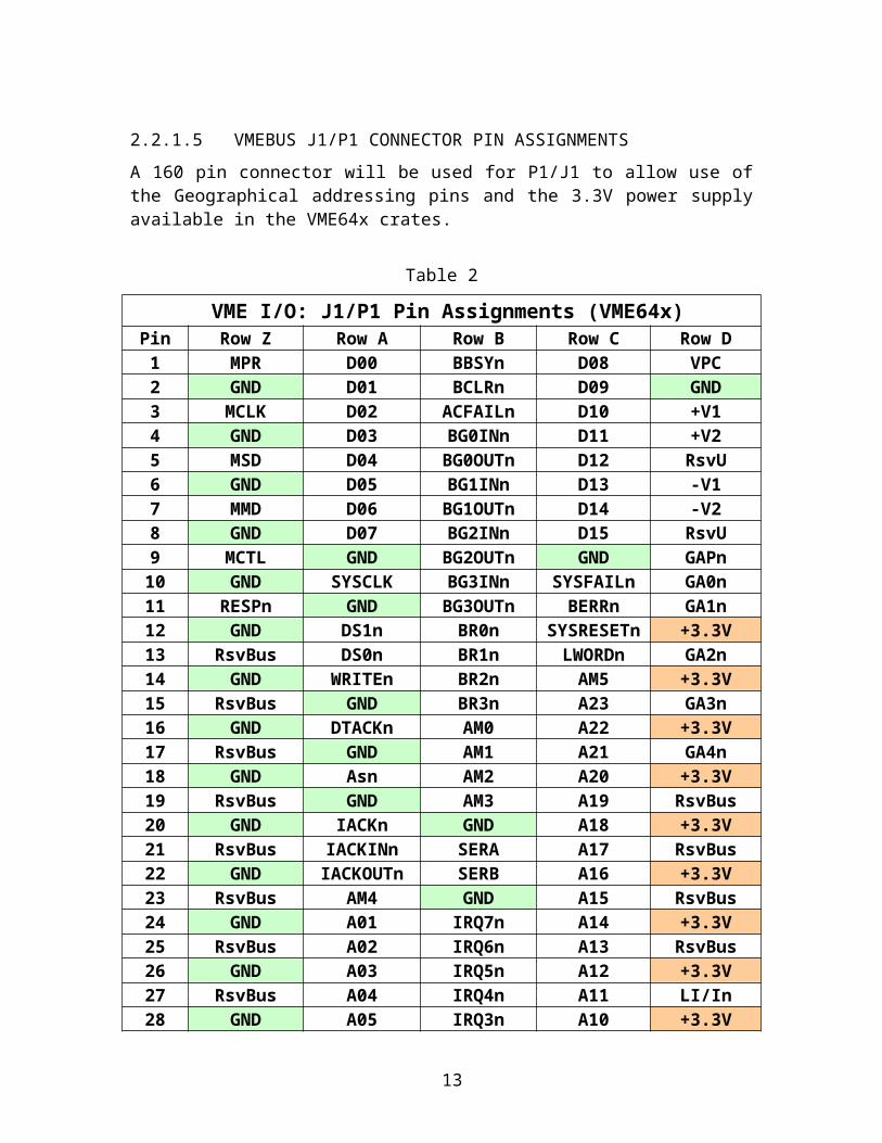
2.2.1.5 VMEBUS J1/P1 CONNECTOR PIN ASSIGNMENTS
A 160 pin connector will be used for P1/J1 to allow use of the Geographical addressing pins and the 3.3V power supply available in the VME64x crates.
Table 2
VME I/O: J1/P1 Pin Assignments (VME64x)Pin Row Z Row A Row B Row C Row D1 MPR D00 BBSYn D08 VPC2 GND D01 BCLRn D09 GND3 MCLK D02 ACFAILn D10 +V14 GND D03 BG0INn D11 +V25 MSD D04 BG0OUTn D12 RsvU6 GND D05 BG1INn D13 -V17 MMD D06 BG1OUTn D14 -V28 GND D07 BG2INn D15 RsvU9 MCTL GND BG2OUTn GND GAPn10 GND SYSCLK BG3INn SYSFAILn GA0n11 RESPn GND BG3OUTn BERRn GA1n12 GND DS1n BR0n SYSRESETn +3.3V13 RsvBus DS0n BR1n LWORDn GA2n14 GND WRITEn BR2n AM5 +3.3V15 RsvBus GND BR3n A23 GA3n16 GND DTACKn AM0 A22 +3.3V17 RsvBus GND AM1 A21 GA4n18 GND Asn AM2 A20 +3.3V19 RsvBus GND AM3 A19 RsvBus20 GND IACKn GND A18 +3.3V21 RsvBus IACKINn SERA A17 RsvBus22 GND IACKOUTn SERB A16 +3.3V23 RsvBus AM4 GND A15 RsvBus24 GND A01 IRQ7n A14 +3.3V25 RsvBus A02 IRQ6n A13 RsvBus26 GND A03 IRQ5n A12 +3.3V27 RsvBus A04 IRQ4n A11 LI/In28 GND A05 IRQ3n A10 +3.3V29 RsvBus A06 IRQ2n A09 LI/On30 GND A07 IRQ1n A08 +3.3V31 RsvBus -12 VDC +5 VSTDBY +12 VDC GND32 GND +5 VDC +5 VDC +5 VDC VPC
11

2.2.1.6 VMEBUS J2/P2 CONNECTOR PIN ASSIGNMENTS
A 96 pin connector will be used for P2/J2 because there are no proposed connections to Row D and Row Z.
Table 3
VME I/O: P2/J2 Pin Assignments (VME64x)Pin Row Z Row A Row B Row C Row D1 UsrDef UsrDef +5 VDC UsrDef UsrDef2 GND UsrDef GND UsrDef UsrDef3 UsrDef UsrDef RETRYn UsrDef UsrDef4 GND UsrDef A24 UsrDef UsrDef5 UsrDef UsrDef A25 UsrDef UsrDef6 GND UsrDef A26 UsrDef UsrDef7 UsrDef UsrDef A27 UsrDef UsrDef8 GND UsrDef A28 UsrDef UsrDef9 UsrDef UsrDef A29 UsrDef UsrDef10 GND UsrDef A30 UsrDef UsrDef11 UsrDef UsrDef A31 UsrDef UsrDef12 GND UsrDef GND UsrDef UsrDef13 UsrDef UsrDef +5 VDC UsrDef UsrDef14 GND UsrDef D16 UsrDef UsrDef15 UsrDef UsrDef D17 UsrDef UsrDef16 GND UsrDef D18 UsrDef UsrDef17 UsrDef UsrDef D19 UsrDef UsrDef18 GND UsrDef D20 UsrDef UsrDef19 UsrDef UsrDef D21 UsrDef UsrDef20 GND UsrDef D22 UsrDef UsrDef21 UsrDef UsrDef D23 UsrDef UsrDef22 GND UsrDef GND UsrDef UsrDef23 UsrDef UsrDef D24 UsrDef UsrDef24 GND UsrDef D25 UsrDef UsrDef25 UsrDef UsrDef D26 UsrDef UsrDef26 GND UsrDef D27 UsrDef UsrDef27 UsrDef UsrDef D28 UsrDef UsrDef28 GND UsrDef D29 UsrDef UsrDef29 UsrDef UsrDef D30 UsrDef UsrDef30 GND UsrDef D31 UsrDef UsrDef31 UsrDef UsrDef GND UsrDef GND32 GND UsrDef +5 VDC UsrDef VPC
12
2.2.2 FRONT END PREAMP AND DIGITIZER
Each GRETINA Digitizer electronics board has 10 front-end input channels. The data signals from the detector amplifiers are transmitted to the digitizer front-end inputs on differential wire pairs in a mass terminated cable assembly. The receptacle connector on the Digitizer is a 100-pin double density D type with 75-mil contact spacing, manufactured by ITT/Cannon, part number 2DD100SBRP. The received input signal is buffered with a true differential input amplifier before the signal is digitized using a 14-bit 100Msps Analog to Digital Converter. The digitized data of all channels is read out simultaneously by a controller/processor FPGA at 200Mbytes/sec/channel.
2.2.2.1 ANALOG INPUT
The analog inputs to the digitizer front-end amplifiers are true differential, high impedance type.
ADD BLOCK DIAGRAM
The pin assignments for the analog input signals are defined in. The labeling for the signals is as follows:
CH1P: Channel 1, positive polarity input signalCH1N: Channel 1, negative polarity input signalSHIELD1: Internal cable shield for Channel 1 wire pair
CH2P: Channel 2, positive polarity input signalCH2N: Channel 2, negative polarity input signalSHIELD2: Internal cable shield for Channel 2 wire pair
………
CH9P: Channel 9, positive polarity input signalCH9N: Channel 9, negative polarity input signalSHIELD9: Internal cable shield for Channel 9 wire pair
CH10P: Channel 10, positive polarity input signalCH10N: Channel 10, negative polarity input signalSHIELD10: Internal cable shield for Channel 10 wire pair
SP1: Auxiliary wire pair connections and shieldSP2: Auxiliary wire pair connections and shieldCONNECT TO FPGA?
13

Table 4
Digitizer Input Interface (100pin ITT Cannon Double Density D Connector, 2DD100SBRP)
Pin Description Pin Description Pin Description Pin Description1 SHIELD10 27 SHIELD102 CH10P 28 CH10N 52 SP2 76 SP23 GND 29 GND 53 GND 77 SP24 GND 30 GND 54 SHIELD9 78 SHIELD95 GND 31 GND 55 CH9N 79 CH9P6 SHIELD8 32 SHIELD8 56 GND 80 GND7 CH8P 33 CH8N 57 GND 81 GND8 GND 34 GND 58 GND 82 GND9 GND 35 GND 59 SHIELD7 83 SHIELD710 GND 36 GND 60 CH7N 84 CH7P11 SHIELD6 37 SHIELD6 61 GND 85 GND12 CH6P 38 CH6N 62 GND 86 GND13 GND 39 GND 63 GND 87 GND14 GND 40 GND 64 SHIELD5 88 SHIELD515 GND 41 GND 65 CH5N 89 CH5P16 SHIELD4 42 SHIELD4 66 GND 90 GND17 CH4P 43 CH4N 67 GND 91 GND18 GND 44 GND 68 GND 92 GND19 GND 45 GND 69 SHIELD3 93 SHIELD320 GND 46 GND 70 CH3N 94 CH3P21 SHIELD2 47 SHIELD2 71 GND 95 GND22 CH2P 48 CH2N 72 GND 96 GND23 GND 49 GND 73 GND 97 GND24 GND 50 GND 74 SHIELD1 98 SHIELD125 SP1 51 SP1 75 CH1N 99 CH1P26 SP1 100 GND
2.2.2.2 FRONT END PREAMP
High impedance input buffers are used to allow the cable termination resistors to dominate the impedance matching of the transmission line and to improve isolation while allowing signal balance on the wire pair. The full-scale amplitude at the input of the front-end amplifier is +/- TBD (1.75V?).
14

2.2.2.3 CENTRAL CONTACT REPEATER OUTPUT
The central contact of the detector shall be connected to the Channel 10 wire pair of the Master Digitizer that is connected to a differential repeater amplifier. The repeater amplifier is used to buffer the Central Contact signal for connection to a front panel LEMO connector. This allows the Central Contact signal to be viewed externally during run-time.
2.2.2.4 DIGITIZER CIRCUIT
The Digitizer circuit will utilize a 100Msps Analog Devices AD6645ASQ-105 ADC for each input channel. The Main FPGA reads out each digitizer channel ADC simultaneously and writes the data to an internal circular buffer in real time.
2.2.3 EVENT FIFO
The Main FPGA writes full events into the Event FIFO after receiving a valid command from the trigger system. The Event FIFO is implemented using two 256Kx18, 7ns FIFO memory chips. Write control is managed solely by the Main FPGA while read control is managed by the Main FPGA through the VME interface.
(start here)
2.2.4 MAIN FPGA
Figure 1 shows the block diagram of the Digitizer. The main FPGA is responsible for control the data acquisition. It uses a Spartan 3 FPGA XC3S5000 (5M gates, 104 Block RAMs) from Xilinx. The configuration memory has 16 M bits and is accessible from VME for in system reconfiguration.
Four Digitizers instrument one crystal. One of these modules is configured as master and is connected to the crystal’s central contact. The other three modules are configured as slaves. The VHDL code for all the 4 modules will be identical which means that we are going to have one part of the code that is the master and another part of the code that is the slave. The master code will be enabled only for the modules that are working as a master while the slave code will be enable in all the modules.
Figure 3 shows a block diagram of the main FPGA. All the FPGA logic is enabled when the module is configured as a master. However, when the module is configured as a slave, the master logic is disabled. The front bus logic receives commands and information from the front bus and either executes the command or sends back the information requested. The VME control block does the communication between the main FPGA and the VME FPGA. This means that the main FPGA access the VME bus only through the VME FPGA. The DAC control block is responsible for retrieving information from the channels, processing it, and controlling the DAC chips. VME registers will configure the processing. The channels block communicates with the FIFO
15

interface. The FIFO interface reads data out of the channel module, and during readout transfers data to the VME control.
ADC
ADC
ADC
ADC
ADC
ADC
ADC
ADC
ADC
ADC
FIFO DAC
VMEFPGA
FBBuffer
SD Chip
FIFOInterface
DACControl
VMEControl
Front BusLogic
MasterLogic
MasterLogicEnable
C.C. LED
C.C. PileUp
EN
Channels
Figure 3: Main FPGA Block Diagram
The channels block implements all the following DSP algorithms:
Leading Edge Discrimination: • yn = xn - xn-k (differentiation)• yn = (xn + xn-2) + xn-1<<1 (´4, Gaussian filtering)• Threshold comparison ® LED time
Constant Fraction Discrimination: • yn = xn - xn-k (differentiation) • yn = (xn + xn-2) + xn-1<<1 (´2, Gaussian filtering)• yn = xn-k- fxn (constant fraction, f is an attenuation factor)• Zero crossing comparison ® CFD time
Trapezoidal filter and energy determination (V.T Jordanov, G.F. Knoll, NIM A345 (1994) 337-345)
• yn = yn-1 + ( (xn + xn-2m-k) )– (xn-m + xn-m-k) )• Maximum tracking ® energy
Pole-Zero correction• yn = xn + In /t (where t is the pre-amplifier time constant)• In = In-1 + xn
16

The master logic block will be enabled by the master logic enable signal. This signal will be sent by the VME FPGA and will indicate to the main FPGA if it is a master or slave module, which will be determined by a VME register.
Table 5 – Master Logic Enable.
Slot Master Enable Board type1 1 Master2 0 Slave3 0 Slave4 0 Slave
The master logic uses the front panel bus to control the four modules connected to a crystal. Also, it interfaces with the serializer/deserializer (SerDes), which communicates with the TTCL. Figure 4 shows the block diagram of the front bus master logic.
Figure 4. Block Diagram of the Front Bus Master Logic
The main logic block coordinates all the others block and interprets the TTCL commands. The SerDes logic is responsible for reading and validating the data package received from the TTCL. This data package is described in [xxx1]. Once it validates the data package, it sends it to the main logic that will then execute the commands required. It is also responsible for sending the information back to the TTCL as well as the fast data. This other data package structure is described in [xxx2]. In order to be able to send the fast data the central contact leading edge (LED) discriminator and the central contact pile up signals are connected directly to this block. The time stamp memory is a set of
17

registers that store all the time stamps that were sent to the TTCL and still point to valid raw data inside the circular buffer.
2.2.4.1 MODES OF OPERATION
The main FPGA will operate in four different modes (see Table 6). When a gamma ray interacts with the crystal, some of the ADC inputs will detect a leading edge (through the LED algorithm). These digitizers will then set a special wired-or line in the front bus (refer to Section 2.2.6) to share the information that an event has taken place (I am not sure I wrote it correctly… we need to understand how do you define “event”).
Table 6. Master Logic Enable.
Mode Board type00 Internal01 External10 Internal with validation11 TTCL
2.2.4.1.1 INTERNAL MODE
In the internal mode all the channels may start an event. But in order for a channel to be able to start an event it needs to be enabled. This will be done by one VME register.
Once a LED of any enabled channel happens then it will set the FB_LED line in the front bus that triggers all the channels. This will start the timers that will latch the results of the DSP algorithms (Energy, CFD, etc). Once all of these results are done, they will be stored in the Header Memory with index 0. After that they will be transferred to the pre-buffer memory.
Finally this data will be readout by the FIFO interface. The FIFO interface is shared with all the 10 channels. It will first add the extra slave or master header (depending if the board is a slave or a master board) and then it will start reading out every channel data package.
This mode can be used with one single board or one full crate without TTCL communication. In this mode it is not expected to have any validation so all the events will be readout.
2.2.4.1.2 EXTERNAL MODE
This mode is very similar to the internal mode. The difference between them is that in this mode the signal that set the FB_LED line in the front bus that triggers all the channels is not set by the LED of one of the channels but by one of the Auxiliary inputs.
18

2.2.4.1.3 INTERNAL WITH VALIDATION MODE
This mode is also very similar to the internal mode. The difference for this mode is that in it the results of the DSP algorithms and the raw data will not be automatically transferred to the pre-buffer memory. They will be waiting for a validation signal. The validation signal will be connected to one of the auxiliary inputs.
2.2.4.1.4 TTCL MODE
While operating in TTCL Mode the crystal crate will be connected through the serdes of the master board to the TTCL.
An event will start when a LED fires form the Central Contact (CC). The CC will be always connected to the Master Digitizer Board on channel 10. The CC LED information will be sent to all the channels in the four boards through a special line in the Front Bus and it will also be sent to the TTCL through the fast data.
Once every channel received the CC LED information they will start the timers that will latch the results of the DSP algorithms (Energy, CFD, etc). Once all of these results are done, they will be stored in a Header Memory specifically defined to this event by the Master Digitizer Board. This means that all the channels are going to be storing the information of one event in the same Header Memory index.
The master board will be calculating the low energy of the CC and will request from the slave board and from itself the hit pattern. When both information are available in the Master Digitizer Board it will wait the TTCL to demand slow data from the digitizer boards, and then it will send these information to the TTCL. The Master Digitizer Board will also store the Time Stamp and the Header Memory index where the results of this event are stored. Once all the steps above are completed the boards are ready to handle another event or to receive a readout command.
Once the TTCL makes a decision that an event needs to be readout it will send to the digitizer boards a readout command and the time stamp of this event. The Master Digitizer Board will then compare this time stamp with all the time stamps that it has stored and are still valid. Valid means that the raw data are still available inside the circular buffer. If the Master Digitizer Board finds a match it will send a readout command to all channels informing which Header Memory needs to be readout.
Once the channels receive the readout command they will transfer the information from the Header Memory and the raw data to the pre-buffer memory. Then they will flag that this pre-buffer is read to be sent to the external FIFO. The FIFO interface is shared with all the 10 channels. It will first add the extra slave or master header (depending if the board is a slave or a master board) and then it will start reading out every channel data package. This concludes the life cycle on an event that was readout.
19

If an event is not going to be readout because the TTCL does not sends a readout command for that particular event it will be flushed out the Header Memory after its corresponding data is over written in the circular buffer.
2.2.4.2 CHECKING SYNCHRONISM
Every channel has its own timer that generates the time stamp. So it is necessary to verify if all channels are in sync. Since the sync command will be sent every 2us and we don’t want to overload the front bus communication we are going to divide this task in two.
Every time the Master Digitizer board receives the sync command it will check the TTCL time stamp against the Central Contact time stamp, if both match then no error flag will be set. This is going to be done at a 2us second rate.
In a slower rate the Master Digitizer Board will be checking the Central Contact time stamp against each channel. This is going to be done by sending a command that latch the current status of all channels as a broadcast command through the Front Bus. Then the Master Digitizer Board will broadcast the CC TS and each channel will compare the CC TS with its latched TS. If there is a mismatch the channel will raise an error flag.
The Master Digitizer Board will send a command to get the status of each board. If there is any error the Master Board will then signalize to the TTCL. No action besides send this information to the TTCL will be done. If a TS reset needs to be done, the TTCL will send specifically a command asking for that. Otherwise this flag will be set forever.
2.2.4.3 INITIALIZATION
2.2.4.3.1 SYSTEM INITIALIZATION
All the board will behave as a slave board after start up or reset. The VME FPGA will set a bit indicating if the board is master and after that the board will enable the master logic block.
The VME FPGA will know that this board is a master board through a VME register.
??????????
2.2.4.3.2 INITIALIZATION OF TTCL COMMUNICATION
During initialization and reset the SERDES link will be down for some period of time while it gets lock. After locking the system will start receiving clock with a 20 ns period.The TTCL will keep the SYNC signal active until its lock signal goes high and this means that the Master Digitizer Board will start receiving nine MSB equals to ‘0’ and nine LSB equals to ‘1’.
20

Once the main FPGA has clock and the system reset goes low, then the Master Digitizer Board will be able to start sending data to the TTCL. Initially it will send sync data allowing the SERDES chip to get lock. After the TTCL SERDES lock then it will start sending real data down to the Master Digitizer Board.
The SD block of the Master Digitizer Board will get out the sync mode once it receives the first data that is different from the sync data. After that a different command will be sent to the main logic of the Master Logic (Figure 4) every 5 clocks.
If the lock signal goes down or a reset happens then the SD Block of the Master Digitizer Board will go back to the sync mode and it will be waiting for the same procedure to happen again in order to start receiving commands.
2.2.4.4 CLOCK MANAGEMENT
The main FPGA has three clock inputs. One of them comes from the VME FPGA and is always present. The second one is the system clock source that comes either from the TTCL link or from the Front Bus. And the third one is an external clock from the auxiliary IOs.
When one board is working by itself the clock may come from the VME FPGA or from the auxiliary IOs. When the boards are working as an independent crate the slave boards will receive their clock through the Front Bus and the Main Digitizer Board will receive its clock from the VME FPGA or the auxiliary IOs.
When working on the TTCL mode the Main Digitizer Board will receive its clock from the recovered clock of the TTCL link and will spread it through the front bus to all the slave boards.
2.2.4.5 OUTPUT DATA FORMAT
The output data package will contain three types of header and the raw data that was read from the ADC. The structure of the data package can be seen on Figure 5
21

Slave Header
Package Header ch0
Raw Data
Package Header ch8
Raw Data
.
.
.
.
.
.
Slave Header
Package Header ch0
Raw Data
Package Header ch9
Raw Data
.
.
.
.
.
.
Master Header
Figure 5 – (a) Data package from a slaver board. (b) Data package from a master board.
The Package header contains the information that belongs to the channels. Its structure is shown in Figure 6.
0 1 2 3 4 5 6 7 8 9 10 11 12 13 14 15 16 17 18 19 20 21 22 23 24 25 26 27 28 29 30 31
Board ID1 Packet length (header included)LED / external timestamp bit 0 - 15* LED / external timestamp bit 16 – 31*
LED / external timestamp bits 32 - 48* Energy bits 0 – 15Energy bit 16 – 24 x x x S E C P CFD Timestamp bit 0 – 15
CFD Timestamp bit 16 - 31 CFD Timestamp bit 32 – 47CFD point 1 bit 0 - 15 CFD point 1 bit 16 – 31CFD point 2 bit 0 - 15 CFD point 2 bit 16 – 31
Raw data point 0 (Sign extended) Raw data point 1 (Sign extended)Raw data point 2 (Sign extended) Raw data point 3 (Sign extended)
.
.
.
.
.
.
Figure 6 – Data Package.
*The TS is updated at 20ns.Notes:S is for the sign of the LED crossing. (1 is negative).E is for external trigger flag (the timestamp is external and LED and CFD are not valid).C is for CFD valid indicating that a CFD crossing occurred.P is for pileup flag indicating that the energy is corrupted.1Board ID will be composed of 4 bits for channel ID and 12 bits for the board serial number.
22

The slave header contains information from the event that is commom to all the channels on that specific board. This slave header is also produced on the Master Digitizer board, once the slave code doesn’t know that it is inside the Master Digitizer Board.
If we want to add an extra header for the Master Board then the FIFO interface will have to know that it is a master board and it has to add the master header to the data package. This changes the structure of the VHDL because now the slave code will be different on the master board. Or is there one way around?
2.2.4.6 Main FPGA Registers REGISTERS
The address shown in the tables that describe the registers are only the bits 9 down to 2. This makes the addresses here compatible with the address written inside the VHDL code.
Description Address Access WidthBoard ID 0x00 R 32
Value is the board serial number that is given by the switch configuration. Bit Value1 0
Bits[11: 0]: Board Id Value Bits[31:12]: TBD
Description Address Access WidthProgramming Done 0x01 R 32
Value is the board serial number that is given by the switch configuration. Bit Value1 0
Bits[9: 0]: Programming status of the channels Bit 10: Programming status of the debug module Bit 11: Programming status of the DAC module Bit 12: and FIFO 0 EF flag Bit 13: and FIFO 1 EF flag Bit 14: and FIFO 0 PAE flag Bit 15: and FIFO 0 HF flag Bit 16: and FIFO 0 PAF flag Bit 17: and FIFO 0 FF flag and FIFO 1 FF flag Bits[31:18]: TBD
Description Address Access WidthExternal Window 0x02 W 32
External validation window length. Value at reset is 0x07FF. Bit Value1 0
Bits[10: 0]: External window length Value Bits[31:11]: TBD
Description Address Access WidthPileup Window 0x03 W 32
Pileup window length. Value at reset 0x0400 (10us). Bit Value1 0
Bits[10: 0]: Pileup window length Value Bits[31:11]: TBD
Description Address Access WidthNoise Window 0x04 W 32
Noise window length. Value at reset 0x0040 (640ns). Bit Value1 0
Bits[ 6: 0]: Noise window length Value Bits[31:11]: TBD
23

Description Address Access WidthExternal trigger sliding length 0x05 W 32Length before we read the energy when we operate in external trigger. Value at reset 0x01C2 (4.5us)
Bit Value1 0
Bits[10: 0]: External trigger sliding length Value Bits[31:11]: TBD
Description Address Access WidthCollection time 0x06 W 32Collection time maximum length (length of the flat top in the trapezoid).Value at reset 0x01C2 (4.5us)
Bit Value1 0
Bits[8: 0]: Collection time Value Bits[31:9]: TBD
Description Address Access WidthIntegration time 0x07 W 32Integration time length (length of one side of the trapezoid). Value at reset 0x01C2 (4.5us)
Bit Value1 0
Bits[8: 0]: Integration time Value Bits[31:9]: TBD
Description Address Access WidthControl/Status channel #Number * RW 32
This register address is the only one that is read/write. Bit Value1 0
Bit 0: START/STOP. This bit must be set to one for the channel to operate. Value at reset is 0. Read/Write. Bit 1: Debug Mode. This bit when set to 1 puts the channel in debug mode operation using internal data. Value at reset 0. (Read/Write) Bit 2: Pile-up drop-out enable. When this bit is set to one, the channel drops any event that occurs in a pileup window else it just notifies pileup through a flag inthe event header. Value at reset 1. Read/Write. Bits [4:3]: Trigger mode. We have the following configuration:00: Internal mode01: External mode10: Internal with Validation mode11: TTCS Decision modeValue a reset: 00. Read/Write. Bit 5: CFD Tap delay setup. If set to 0, the tap delay is filling-up and no event can be acquired. Read-only. Bit 6: Tap delay 1 setup. If set to 0, the tap delay is filling-up and no event can be acquired. Read-only. Bit 7: Tap delay 2 setup. If set to 0, the tap delay is filling-up and no event can be acquired. Read-only. Bit 8: Tap delay 3 setup. If set to 0, the tap delay is filling-up and no event can be acquired. Read-only. Bit 9: Tap delay 4 setup. If set to 0, the tap delay is filling-up and no event can be acquired. Read-only. Bits [11:10]: Polarity validation. Value at reset 11.01: only positive trigger considered10: only negative trigger considered11: both triggers considered00: no trigger considered (the LED still firesexternally though, as opposed toSTART/STOP) Read/Write. Bits[14:12]: TBD Bit 15: Pre-buffer Ready flag Bits[31:16]: TBD
* There is one of this registers for each channels and their address are specified by the next table.
Description Address Access WidthControl/Status channel 0 0x10 RW 32Control/Status channel 1 0x11 RW 32Control/Status channel 2 0x12 RW 32
24

Control/Status channel 3 0x13 RW 32Control/Status channel 4 0x14 RW 32Control/Status channel 5 0x15 RW 32Control/Status channel 6 0x16 RW 32Control/Status channel 7 0x17 RW 32Control/Status channel 8 0x18 RW 32Control/Status channel 9 0x19 RW 32
Description Address Access WidthLED Threshold * W 32This is the LED threshold. Only bits 17 to 0 are used. This is an unsigned value and the three lower bits are extra precision bit. (The dot is between bit 3 and 2).The value at reset is 0x7FFF (full range so that no event should trigger). It is internally converted to a signed value depending on how the sign of the current sample is.Write-only.
Bit Value
1 0
Bits[17: 0]: LED Threshold Value Bits[31:18]: TBD
* There is one of this registers for each channels and their address are specified by the next table.
Description Address Access WidthControl/Status channel 0 0x20 W 32Control/Status channel 1 0x21 W 32Control/Status channel 2 0x22 W 32Control/Status channel 3 0x23 W 32Control/Status channel 4 0x24 W 32Control/Status channel 5 0x25 W 32Control/Status channel 6 0x26 W 32Control/Status channel 7 0x27 W 32Control/Status channel 8 0x28 W 32Control/Status channel 9 0x29 W 32
Description Address Access WidthCFD Parameters * W 32Bit 12-7: CFD delay. Value at reset is 0x3F giving a delay of 630ns. Write-onlyBit 6-5: CFD fraction. It is a value indicating what fraction is used (see table 9 for values). Value at reset is “00” giving a fraction of 0.5. Write-onlyBit 4-0: CFD threshold. It is an unsigned value of the CFD threshold. The dot is after bit 0. Value at reset is 0x10 (160kev). Write-only
Bit Value
1 0
Bits[ 4: 0]: CFD threshold Value Bits[ 6: 5]: CFD fraction Value Bits[12: 7]: CFD delay Value Bits[31:13]: TBD
* There is one of this registers for each channels and their address are specified by the next table.
Description Address Access WidthControl/Status channel 0 0x30 W 32Control/Status channel 1 0x31 W 32Control/Status channel 2 0x32 W 32Control/Status channel 3 0x33 W 32Control/Status channel 4 0x34 W 32Control/Status channel 5 0x35 W 32Control/Status channel 6 0x36 W 32Control/Status channel 7 0x37 W 32Control/Status channel 8 0x38 W 32Control/Status channel 9 0x39 W 32
Description Address Access WidthRaw data sliding length * W 32Delay before we start retrieving raw data. Only bits 10 to 0 are used. Value at reset is 0x01C2 (4.5us). Write-only
Bit Value1 0
Bits[10: 0]: Raw data sliding length Value Bits[31:11]: TBD
* There is one of this registers for each channels and their address are specified by the next table.
25

Description Address Access WidthControl/Status channel 0 0x40 W 32Control/Status channel 1 0x41 W 32Control/Status channel 2 0x42 W 32Control/Status channel 3 0x43 W 32Control/Status channel 4 0x44 W 32Control/Status channel 5 0x45 W 32Control/Status channel 6 0x46 W 32Control/Status channel 7 0x47 W 32Control/Status channel 8 0x48 W 32Control/Status channel 9 0x49 W 32
Description Address Access WidthRaw data window * W 32Length of raw data retrieved. Only bits 9 to 0 are used. Value at reset is 0x32 (500ns). Write-only
Bit Value1 0
Bits[ 9: 0]: Raw data length Value Bits[31:10]: TBD
* There is one of this registers for each channels and their address are specified by the next table.
Description Address Access WidthControl/Status channel 0 0x50 W 32Control/Status channel 1 0x51 W 32Control/Status channel 2 0x52 W 32Control/Status channel 3 0x53 W 32Control/Status channel 4 0x54 W 32Control/Status channel 5 0x55 W 32Control/Status channel 6 0x56 W 32Control/Status channel 7 0x57 W 32Control/Status channel 8 0x58 W 32Control/Status channel 9 0x59 W 32
Description Address Access WidthDebug data buffer address 0x60 W 32Used by debug module (see section XIII of the Gretina VHDL modules description document).
Bit Value1 0
Bits[31: 0]: Value
Description Address Access WidthDebug data buffer data 0x61 W 32Used by debug module (see section XIII of the Gretina VHDL modules description document).
Bit Value1 0
Bits[31: 0]: Value
Description Address Access WidthLED Flag window 0x62 W 32Number of clock cycles the LED flag is kept raise on the Fast Data. Range varies from 1 (10ns) to 1024 (~1us).
Bit Value1 0
Bits[31: 0]: Value
Description Address Access WidthInternal Mode operation Mask 0x63 W 32When operating in internal mode this register enable the channels that can write on the fast signal on the FB Leading edge detected.
Bit Value1 0
Bits[10: 0]: Channels that are enabled Value Bits[31:10]: TBD
Description Address Access WidthFront Bus Enabled 0x64 W 32This is only used if the board in not working on the TTCL mode. If the front bus is enable means that we have a full crate (four boards, one master and three slaves) otherwise the board is working by itself.
Bit Value
1 0
Bit 0: Front Bus enabled Value
26

Bits[31: 1]: TBD Value
2.2.5 DAC OUTPUTS
The GRETINA Digitizer will utilize 2 general-purpose 100MHz Digital to Analog converters (DAC) that will have outputs available at the front panel of the module. The design will be implemented with current output DACs to allow signal summing using a NIM module. The board will be designed to allow the option of loading the circuit as a differential voltage output DAC if required. The option must be selected at the time that the board is assembled and will not be user selectable in the system. Signals required by the DACs: Clock and 8 bit data word. (Analog Devices AD9748ACP)
2.2.6 FRONTBUS INTERFACE
The FrontBus Interface will be used by the Master Digitizer to distribute the system clock and to communicate with the three Slave Digitizers in each VME crate. The Master will set some control registers asking the boards to execute some task and will read and write from other registers in order to transfer information. The Master Digitizer is always connected to the Central Contact of the Crystal, so the time require to fetch hit patterns will not affect the ability to supply information to the “Fast Decision Trigger” algorithms.
The 50MHz System Clock is recovered from the Serial Data transmitted by the Global Trigger and Timing crate and then routed as a differential pair to all of the Digitizers over the FrontBus. The 50MHz clock is multiplied to 100MHz in the Main FPGA and then used to digitize the input data for each channel.
Pin Count - 40STROBE –Starts transaction (it has a internal pull up resistor)READWRITE BASE ADDR (3)REG ADDR (5)DATA (10)GND (10) {1 per every 3 signals}DIFF PAIR (4)WIRED-OR (2)SPARES (3)
FRONT Bus Interface System Clock: Differential 2The system clock …..
27

Figure 7: FRONTBUS CLOCK DISTRIBUTION
1. Data Bus: 10 bit bi-directional parallel busa. Valid data latched on each clock transitionb. The data and command bus are implemented using standard LVT245
transceivers (Bus Hold and built in series termination resistors)
2. Address Bus: 3 bits wide
Table 7 – Front Bus Address.
Front Bus Address
Target Device for Read Access only
000 Digitizer 0 (Master)001 Digitizer 1010 Digitizer 2011 Digitizer 3
For Read access, the Master activates one Digitizer per complete cycle.
3. Command Bus 4 bits wide
Table 8 – Front Bus command.
Front Bus Command
Command Name Command Description
0111 Write trigger data to slave. This command performs a read out operation and will send the Header Memory index in the data.
0001 Reset TS All time stamps will be reset.
28

0010 Send TS Send the time stamp that will be compared with the channel TS to verify if they are in sync
0011 Get Status Read the status of every board. *Data contains the information about which status is going to be readout.
0100 Fetch hit pattern Read the hit pattern.0101 Latch status Latch the status of all channels in the same
time, so it is possible to compare the TS of the channels.
0110 Calibration Inject 0000 IDLE Do nothing.
* This is an option if we want to have more then 10 bits of status for every board.
4. Leading Edge Detect Wired-OR signal – 1 bitThis signal is used to indicate that a detector crystal has detected a leading edge.
29

Table 9 - Frontbus Interface
Frontbus Interface (34-pin MT Connector AMP)
Pin NAME Description1 CLK_IO_P FB Clock positive polarity2 CLK_IO_N FB Clock negative polarity3 GND Board Ground4 GND Board Ground5 DATA(0) FB Data Bus Bit 06 DATA(1) FB Data Bus Bit 17 GND Board Ground8 DATA(2) FB Data Bus Bit 29 DATA(3) FB Data Bus Bit 310 GND Board Ground11 DATA(4) FB Data Bus Bit 412 DATA(5) FB Data Bus Bit 513 GND Board Ground14 DATA(6) FB Data Bus Bit 615 DATA(7) FB Data Bus Bit 716 GND Board Ground17 DATA(8) FB Data Bus Bit 818 DATA(9) FB Data Bus Bit 919 GND Board Ground20 ADDR(0) FB Address Bit 021 ADDR(1) FB Address Bit 122 GND Board Ground23 ADDR(2) FB Address Bit 224 CMD(0) FB Command Bit 025 GND Board Ground26 CMD(1) FB Command Bit 127 CMD(2) FB Command Bit 228 GND Board Ground29 CMD(3) FB Command Bit 330 SPARE Spare Pin31 SPARE Spare Pin32 GND Board Ground33 SPARE Spare Pin34 SPARE Spare Pin35 GND Board Ground36 SPARE W-OR Spare Pin (Wired OR)37 LE DETECT FB Leading Edge Detect (Wired OR)38 GND Board Ground39 SP DIFF PAIR Spare Pin DIFF40 SP DIFF PAIR Spare Pin DIFF
There will be two types of commands for the Front Bus, the read and write. The signal will be asserted on the falling edge of the clock and will be valid on the raising edge of the clock. The timing diagrams of these two commands are shown in Figure 8 and Figure9.
30

During a reset all the modules will start working as slave, so none of them are going to be driving the control signals. The Strobe*1 line is the signal that tells the board that a new command needs to be executed. In order to avoid any false commands from being executed right after a reset this line will have a pull-up resistor.
DATA
CLK
Address
Strobe*
ZZ Data
XX
ZZ
Address XX
RNW XX XX
Figure 8: Front Bus communication timing diagram – master write operation.
DATA
CLK
Address
Strobe*
ZZ Data
XX
ZZ
Address XX
RNW XX XX
Figure 9: Front Bus communication timing diagram – master read operation.
1 * means that the signal has its logic inverted.
31

2.2.6.1 Registers for the Front Bus
Description Address Access WidthSlave Board 0 Hit Pattern 0x00 RW 10Hit pattern of the latest hit that happened in the board with slave address #0. This board is also the Master board.
Bit Value1 0
Bits[9: 0]: Hit Pattern Value
Description Address Access WidthSlave Board 1 Hit Pattern 0x01 RW 10Hit pattern of the latest hit that happened in the board with slave address #1.
Bit Value1 0
Bits[9: 0]: Hit Pattern Value
Description Address Access WidthSlave Board 2 Hit Pattern 0x02 RW 10Hit pattern of the latest hit that happened in the board with slave address #2.
Bit Value1 0
Bits[9: 0]: Hit Pattern Value
Description Address Access WidthSlave Board 3 Hit Pattern 0x03 RW 10Hit pattern of the latest hit that happened in the board with slave address #3.
Bit Value1 0
Bits[9: 0]: Hit Pattern Value
Description Address Access WidthTime stamp 0 0x04 RW 10These are part of the 48 bits of the time stamp that will be used the check the synchronism of the system.
Bit Value1 0
Bits[9: 0]: Time stamp bits [ 9: 0] Value
Description Address Access WidthTime stamp 1 0x05 RW 10These are part of the 48 bits of the time stamp that will be used the check the synchronism of the system.
Bit Value1 0
Bits[9: 0]: Time stamp bits [19:10] Value
Description Address Access WidthTime stamp 2 0x06 RW 10These are part of the 48 bits of the time stamp that will be used the check the synchronism of the system.
Bit Value1 0
Bits[9: 0]: Time stamp bits [29:20] Value
Description Address Access WidthTime stamp 3 0x07 RW 10These are part of the 48 bits of the time stamp that will be used the check the synchronism of the system.
Bit Value1 0
Bits[9: 0]: Time stamp bits [39:30] Value
Description Address Access WidthTime stamp 1 0x08 RW 10These are part of the 48 bits of the time stamp that will be used the check the synchronism of the system.
Bit Value1 0
Bits[7: 0]: Time stamp bits [47:40] Value
32

Bits[9: 8]: TBD Value
2.2.7 SERIALIZER/DESERIALIZER
Part: National Semiconductor DS92LV18TVV Connector : Shielded RJ45 connector
1. LVDS Transmit 2. LVDS Receive
a. Recovers 50MHz system clock from serial data stream
System Clock generated by the Global Trigger Module through G-Link serial communication channel.
Discussion of Digitizer-to-Digitizer Communication-Added complication to HardwareInterface is full duplexProtocol – defined by G-Link device
Add reference to JTA SER/DES docs on DocDB
2.2.8 AUXILLIARY INPUT INTERFACE
16 inputs max, .1x.1 header 1 ground per input pin.
2.2.9 100MHZ CLOCK DISTRIBUTION
The MAIN FPGA will generate a 100MHz clock from the recovered 50MHz system clock and this clock will by distributed as an LVDS signal to all of the Analog Front Ends. List Part -- State skews and delays
2.2.10 FRONT PANEL LED INDICATORS
18 FP LED indicators1 per Digitizer Channel, Bi-Color, Green/Yellow (10)Definition:
Channel Off LED OffChannel On GREEN SolidTaking Data GREEN BlinkingFIFO Readout YELLOW SolidRate OVR YELLOW Blinking
VME Activity YELLOWFPGA READY GREEN+3.3V DC GREEN+5.0V DC GREEN-5.0V DC GREEN3 TBD Controlled by Main FPGA
33

2.2.11 VOLTAGE MONITORS
Voltage monitor chip on boardMonitored Voltages: +3.3V, +5.0V, -5.0V, +1.2V (Main FPGA)Powered by +12V in to board
Power-OK connected to Power on reset circuitPower-OK Over-Voltage Fault and under voltage fault to VME FPGA
2.2.12 TEMPERATURE MONITORS
Three temperature monitor switches that trip if board temp exceed 70C. Connected to VME FPGA. Can be used to hold the Main FPGA in a reset state
34

Time Stamp data --Sync signal to synchronize time stamp counters of all boardsStore data in temporary buffer - Circular buffer to cover latency of trigger system, 20us FIFO buffer for portion of 20us circular buffer to be readGenerate trigger primitives-- Running trigger total Receive trigger -- Readout pattern of segments in crystal based on look-up tableInformation to send from Digitizers to global trigger: channel ID 2bytesLED time 6 bytesLow resolution energy 2 bytes10 Mbytes/sec per crystal (from PEP)a gamma-ray interacts with 20 segments. Each interaction interacts with 9 segments => 2.3 hits per gamma ray. (Electronic req. document)2400 bytes/gamma-ray (Electronic req. document)10Mbytes/2400= ~4200 interaction/sec.xtal => 2.3 * 4200 = ~10k hits/sec.xtalWe send 10 bytes to the trigger per segment that collect the charge (see 10/28/05)Therefore, if we funnel all the info thru just one serial connection we have a total of: 30 xtals * 10 * 10k = 3 MbytesTherefore, ~30 Mbits/sec if all information of the trigger passes thru just one serializer.So, a serializer with 50 Mbits/sec will be enough.
10/24/2005Trigger:Energy: we need to send the lower resolution energy information from the digitizer to the Global trigger.Auxiliary detector trigger: the digitizers need to send the Level-1 trigger decision to the global trigger even for auxiliary detector trigger.Level-1 trigger is generated by the digitizers, energy above some thresholdLevel-2 trigger: global triggerHow to recognize the “main hit”, in comparison with a waveform adjacent to the main hit? The waveform has to be above threshold even after 500 ns (or 450 ns?… because there are these few samples we need to save before the hit itself)Level-1 trigger will always done after ~500 ns after the hit.The info to read before the LED is settable.What happen if we have two hits in the same segment or central contact within 10 usecs? The waveform will be dropping to zero, and the second hit comes, and it adds to the first hit. What threshold do we use now? The output of the pre-amp was still above threshold when the second hit happened…What information the trigger has to send back:… next time…. for low resolution energy we should use a form of filtering (like trapezoidal), just with smaller number of samples. The low-res discriminator will be used by the digitizer to make the determination if the segment sees net charge.
Trigger losses: we need to recognize the segment that collected the charge. One procedure is described above. What about the dead time? That one segment will not recognize another event until the ADC trace is fully store. Is this correct? This should impact the dead time requirement.
What about a moving threshold depending on the pile-up in the pre-amplifier??? There is a triangular differentiator inside the FPGA that differentiate twice before going to the LED and 4 x before the CFD.
What information we received back from the trigger? At least channel ID, just the ID that detects net charge and the time stamp. The digitizer will have the map of the crystal to know which channels they need to readout. The crystal “map” has to be downloaded from the VME host.
The beginning time before the LED and the length of the of the waveform recorded has to be programmable.
If there is a pile-up condition (detected by the 2x differentiator), we tag this event.If two pulses within ~100 ns the pile-up will not detect this condition.pipeup is a problem after the filtering of LED and the energy calculation. As long as the pile-up is spaced more than the 10 us for high resolution energy determination, we will not see the effect.IY suggests that the trapezoidal filter will take care of the energy measurement, even in the case of pile-up. We need to check.
The trapezoidal filter has to be programmable.
Segment ControlEach segment will have a number of user-controlled parameters. For example there should be a method of turning off individual segments in case they become noise or defective.
Trigger LatencyWhen GRETINA is running by itself, with no trigger data from auxiliary detectors, it is desirable to keep the trigger latency as short as possible. In this case the total time from a level-1 trigger till the return of the level-2 trigger can be no longer than 20usec. This latency includes the time it takes the trigger data to reach the trigger module, the time it takes the trigger module to process the data, and how long it takes the level-2 trigger notification to get back to the digitizer modules. It should be noted that this latency determines how long the data storage (pipelines) must be in the digitizer modules.
When GRETINA is running with auxiliary detectors it is desirable to make the trigger latency as long as possible. The longer latency in this case will allow us to interface with slower devices and interactions. The limiting factor on how long this latency can be will be how large you can make the storage pipeline in the digitizer modules. It is desirable to be able to make this latency 100 usec when interfacing with auxiliary detectors.
Time Stamp IncrementThe time stamp in the digitizer modules shall be incremented at least once every 10 nsec. It will use the same clock as the ADCs.The time stamp will be 48 bits (52 bits) and will be clocked once every 10 nsec (1 nsec?). Clock Synchronization and verificationThere needs to be a method to synchronize all of the time stamp clocks to the same value in the digitizer modules and auxiliary detectors. This could be implemented with a common pulser for all preamps.
There also needs to be a method to verifying the time stamp synchronization between segments. This method should be independent of the clock distribution tree.
Harold feels that it will be difficult to adjust all pre-amplifiers in the same way to use them to check the clock synchronization.There is a differential amplifier going to each ADC. They have a common input, which we could exercise to synchronize.10 ns clock = 100 MHz. Time increments by 10 ns clock ticks, this clock is distributed by the serial communication.If we send a command thru the serializer to reset and stop all time stamps. Then we send a command to start counting the time stamp, them all time stamps should be synchronized.It get decoupled of reset the boards. How to check it they are in synch????Requirement: we have to be able to independently verify the time stamp: to have a “charge inject” like signal generated by the calibration system. This “charge inject” like is a LVDS signal, that can be multiply by 4 (with a buffer) in the detector side. It can also be passive. It feeds back to the digitizer thru the 11th pair available in the cable.If we verify with the precision of +/- 1 time stamp, is this adequate???
DIGITIZERSProcedure to check the synchronizationWhat is the algorithm to recognize the contact that collected all the charge?We need this information to tell the other digitizers connected to the same crystal that they need to readout the adjacent channels in the circular buffers.Host computer will check the trigger info? If there is local communication between the digitizers, how we arbitrate when the host wants to access the same information?Harold: has a concern that, if the gamma-ray goes from one crystal to the other, and not a lot of energy is left in the gamma-ray, do we have to force the readout of adjacent crystals
35