General Description Features - Diodes Incorporated · Battery Powered Equipment Figure 1. Package...
29
Data Sheet 1 Dec. 2012 Rev. 2. 6 BCD Semiconductor Manufacturing Limited HIGH SPEED, EXTREMELY LOW NOISE LDO REGULATOR AP2121 General Description The AP2121 series are positive voltage regulator ICs fabricated by CMOS process. Each of these ICs con- sists of a voltage reference, an error amplifier, a resis- tor network for setting output voltage, a current limit circuit for current protection and a chip-enable circuit (5-pin products only). The AP2121 series feature high supply voltage ripple rejection, low dropout voltage, low noise, high output voltage accuracy, and low current consumption which make them ideal for use in various battery-powered devices. The AP2121 series have 1.2V, 1.3V, 1.5V, 1.8V, 2.5V, 2.8V, 2.85V, 3.0V, 3.2V and 3.3V versions. The AP2121 are available in standard SOT-23-3, SOT- 23-5 and CSP-4 packages. Features · Low Dropout Voltage at I OUT =100mA: 150mV Typical (Except 1.2V, 1.3V and 1.5V Versions) · Low Standby Current: 0.1μA Typical · Low Quiescent Current: 25μA Typical · High Ripple Rejection: 70dB Typical (f=1kHz) · Output Current: More Than 200mA (300mA Limit) · Extremely Low Noise: 30μVrms (10Hz to 100kHz) · Excellent Line Regulation: 4mV Typical · Excellent Load Regulation: 12mV Typical · High Output Voltage Accuracy: ±2% · Excellent Line Transient Response and Load Transient Response · Compatible with Low ESR Ceramic Capacitor (as Low as 1μF) Applications · Mobile Phones, Cordless Phones · Wireless Communication Equipment · Portable Games · Cameras, Video Recorders · Sub-board Power Supplies for Telecom Equip- ment · Battery Powered Equipment Figure 1. Package Types of AP2121 SOT-23-5 SOT-23-3 CSP-4
Transcript of General Description Features - Diodes Incorporated · Battery Powered Equipment Figure 1. Package...

Data Sheet
1
Dec. 2012 Rev. 2. 6 BCD Semiconductor Manufacturing Limited
HIGH SPEED, EXTREMELY LOW NOISE LDO REGULATOR AP2121
General Description
The AP2121 series are positive voltage regulator ICsfabricated by CMOS process. Each of these ICs con-sists of a voltage reference, an error amplifier, a resis-tor network for setting output voltage, a current limitcircuit for current protection and a chip-enable circuit(5-pin products only).
The AP2121 series feature high supply voltage ripplerejection, low dropout voltage, low noise, high outputvoltage accuracy, and low current consumption whichmake them ideal for use in various battery-powereddevices.
The AP2121 series have 1.2V, 1.3V, 1.5V, 1.8V, 2.5V,2.8V, 2.85V, 3.0V, 3.2V and 3.3V versions.
The AP2121 are available in standard SOT-23-3, SOT-23-5 and CSP-4 packages.
Features
· Low Dropout Voltage at IOUT=100mA: 150mVTypical (Except 1.2V, 1.3V and 1.5V Versions)
· Low Standby Current: 0.1μA Typical· Low Quiescent Current: 25μA Typical· High Ripple Rejection: 70dB Typical (f=1kHz)· Output Current: More Than 200mA (300mA
Limit)· Extremely Low Noise: 30μVrms (10Hz to
100kHz) · Excellent Line Regulation: 4mV Typical· Excellent Load Regulation: 12mV Typical· High Output Voltage Accuracy: ±2%· Excellent Line Transient Response and Load
Transient Response· Compatible with Low ESR Ceramic Capacitor (as
Low as 1μF) Applications
· Mobile Phones, Cordless Phones· Wireless Communication Equipment · Portable Games· Cameras, Video Recorders· Sub-board Power Supplies for Telecom Equip-
ment· Battery Powered Equipment
Figure 1. Package Types of AP2121
SOT-23-5SOT-23-3 CSP-4

Data Sheet
2
Dec. 2012 Rev. 2. 6 BCD Semiconductor Manufacturing Limited
HIGH SPEED, EXTREMELY LOW NOISE LDO REGULATOR AP2121
Pin Configuration
Figure 2. Pin Configuration of AP2121 (Top View)
K Package (SOT-23-5)
NC
VOUT
VIN
GND
CE
N Package (SOT-23-3)
VIN
GND
VOUT
Pin Description
Pin NumberPin Name Function
SOT-23-3 SOT-23-5 CSP-4(J4/J4A)
CSP-4(J4C/J4B)
3 1 A2 A1 VIN Input voltage
1 2 B1 B2 GND Ground
3 A1 B1 CE Active high enable input pin. Logic high=enable, logic low=shutdown
4 NC No connection
2 5 B2 A2 VOUT Regulated output voltage
J4/J4A Package(CSP-4 (P 0.5)/CSP-4 (P 0.4))
3
21
1
2
3 4
5
A1 A2
B1 B2
Pin 1 Mark CE VIN
GND VOUT
A1 A2
B1 B2
Pin 1 Mark
CE
VIN
GND
VOUT
J4C/J4B Package(CSP-4 (P 0.5)/CSP-4 (P 0.4))
Data Sheet
3
Dec. 2012 Rev. 2. 6 BCD Semiconductor Manufacturing Limited
HIGH SPEED, EXTREMELY LOW NOISE LDO REGULATOR AP2121
Functional Block Diagram
Figure 3. Functional Block Diagram of AP2121
SOT-23-5/CSP-4(J4/J4A)/CSP-4(J4C/J4B)
VREF
CURRENT LIMIT
VREF
CURRENT LIMIT
VIN
CE
VOUT
GND2/B1/B23/A1/B1
1/A2/A1 5/B2/A2VIN VOUT
GND1
3 2
SOT-23-3
Data Sheet
4
Dec. 2012 Rev. 2. 6 BCD Semiconductor Manufacturing Limited
HIGH SPEED, EXTREMELY LOW NOISE LDO REGULATOR AP2121
Package Temperature Range Condition
Part Number Marking ID Packing TypeLead Free Green Lead Free Green
SOT-23-3 -40 to 85oC
AP2121N-1.2TRE1 AP2121N-1.2TRG1 EF9 GF9 Tape & Reel
AP2121N-1.3TRE1 AP2121N-1.3TRG1 EG9 GG9 Tape & Reel
AP2121N-1.5TRE1 AP2121N-1.5TRG1 EF1 GF1 Tape & Reel
AP2121N-1.8TRE1 AP2121N-1.8TRG1 EF3 GF3 Tape & Reel
AP2121N-2.5TRE1 AP2121N-2.5TRG1 EF4 GF4 Tape & Reel
AP2121N-2.8TRE1 AP2121N-2.8TRG1 EF5 GF5 Tape & Reel
AP2121N-3.0TRE1 AP2121N-3.0TRG1 EF6 GF6 Tape & Reel
AP2121N-3.2TRE1 AP2121N-3.2TRG1 EF7 GF7 Tape & Reel
AP2121N-3.3TRE1 AP2121N-3.3TRG1 EF8 GF8 Tape & Reel
SOT-23-5 -40 to 85oC
Active High (Pull-down resistor built-in) AP2121AK-1.2TRE1 AP2121AK-1.2TRG1 E1T G1T Tape & Reel
Active High (Pull-down resistor built-in) AP2121AK-1.3TRE1 AP2121AK-1.3TRG1 E1R G1R Tape & Reel
Active High (Pull-down resistor built-in) AP2121AK-1.5TRE1 AP2121AK-1.5TRG1 E1Z G1Z Tape & Reel
Active High (Pull-down resistor built-in) AP2121AK-1.8TRE1 AP2121AK-1.8TRG1 E1U G1U Tape & Reel
Active High (Pull-down resistor built-in) AP2121AK-2.5TRE1 AP2121AK-2.5TRG1 E1V G1V Tape & Reel
Active High (Pull-down resistor built-in) AP2121AK-2.8TRE1 AP2121AK-2.8TRG1 E1W G1W Tape & Reel
Active High (Pull-down resistor built-in) AP2121AK-3.0TRE1 AP2121AK-3.0TRG1 E1X G1X Tape & Reel
Active High (Pull-down resistor built-in) AP2121AK-3.2TRE1 AP2121AK-3.2TRG1 E3Z G3Z Tape & Reel
Active High (Pull-down resistor built-in) AP2121AK-3.3TRE1 AP2121AK-3.3TRG1 E1Y G1Y Tape & Reel
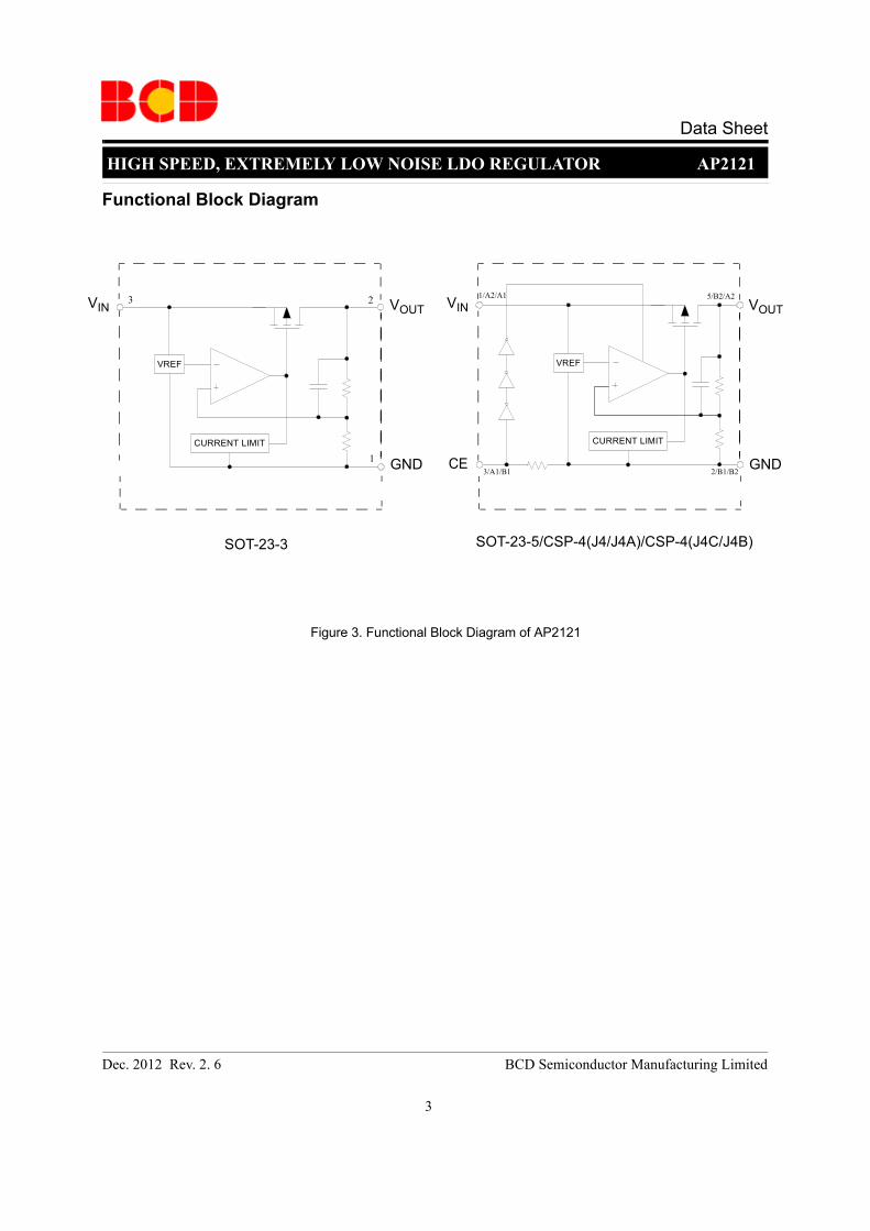
Circuit Type
Package
E1: Lead Free
AP2121 -
TR: Tape and Reel
Ordering Information
1.5: Fixed Output 1.5V
2.5: Fixed Output 2.5VN: SOT-23-3
2.85: Fixed Output 2.85VK: SOT-23-5
A: Active High (Pull-down resistor built-in)
Blank: No Enable Function
1.8: Fixed Output 1.8V
2.8: Fixed Output 2.8V
3.0: Fixed Output 3.0V3.2: Fixed Output 3.2V
1.3: Fixed Output 1.3V1.2: Fixed Output 1.2V
G1: Green
J4: CSP-4(P 0.5)J4A: CSP-4 (P 0.4)
3.3: Fixed Output 3.3V J4C: CSP-4(P 0.5) J4B: CSP-4 (P 0.4)
5
Dec. 2012 Rev. 2. 6 BCD Semiconductor Manufacturing Limited
HIGH SPEED, EXTREMELY LOW NOISE LDO REGULATOR AP2121
Data Sheet
Package Temperature Range Condition
Part Number Marking ID Packing TypeLead Free Green Lead Free Green
CSP-4 -40 to 85oC
0.4 Pitch AP2121AJ4A-1.2TRG1 CB Tape & Reel
0.4 Pitch AP2121AJ4A-1.3TRG1 CC Tape & Reel
0.4 Pitch AP2121AJ4A-1.5TRG1 CD Tape & Reel
0.4 Pitch AP2121AJ4A-1.8TRG1 CE Tape & Reel
0.4 Pitch AP2121AJ4A-2.5TRG1 CF Tape & Reel
0.4 Pitch AP2121AJ4A-2.8TRG1 CG Tape & Reel
0.4 Pitch AP2121AJ4A-2.85TRG1 DD Tape & Reel
0.4 Pitch AP2121AJ4A-3.0TRG1 CH Tape & Reel
0.4 Pitch AP2121AJ4A-3.2TRG1 DA Tape & Reel
0.4 Pitch AP2121AJ4A-3.3TRG1 DB Tape & Reel
CSP-4 -40 to 85oC
0.5 Pitch AP2121AJ4-1.2TRG1 BA Tape & Reel
0.5 Pitch AP2121AJ4-1.3TRG1 BB Tape & Reel
0.5 Pitch AP2121AJ4-1.5TRG1 BC Tape & Reel
0.5 Pitch AP2121AJ4-1.8TRG1 BD Tape & Reel
0.5 Pitch AP2121AJ4-2.5TRG1 BE Tape & Reel
0.5 Pitch AP2121AJ4-2.8TRG1 BF Tape & Reel
0.5 Pitch AP2121AJ4-2.85TRG1 DC Tape & Reel
0.5 Pitch AP2121AJ4-3.0TRG1 BG Tape & Reel
0.5 Pitch AP2121AJ4-3.2TRG1 BH Tape & Reel
0.5 Pitch AP2121AJ4-3.3TRG1 CA Tape & Reel
Ordering Information (Continued)

Data Sheet
6
Dec. 2012 Rev. 2. 6 BCD Semiconductor Manufacturing Limited
HIGH SPEED, EXTREMELY LOW NOISE LDO REGULATOR AP2121
Ordering Information (Continued)
BCD Semiconductor's Pb-free products, as designated with "E1" suffix in the part number, are RoHS compliant. Products with"G1" suffix are available in green packages.
Package Temperature Range Condition
Part Number Marking ID Packing TypeLead Free Green Lead Free Green
CSP-4 -40 to 85oC
0.4 Pitch AP2121AJ4B-1.2TRG1 DE Tape & Reel
0.4 Pitch AP2121AJ4B-1.3TRG1 DF Tape & Reel
0.4 Pitch AP2121AJ4B-1.5TRG1 DG Tape & Reel
0.4 Pitch AP2121AJ4B-1.8TRG1 DH Tape & Reel
0.4 Pitch AP2121AJ4B-2.5TRG1 EA Tape & Reel
0.4 Pitch AP2121AJ4B-2.8TRG1 EB Tape & Reel
0.4 Pitch AP2121AJ4B-2.85TRG1 EC Tape & Reel
0.4 Pitch AP2121AJ4B-3.0TRG1 ED Tape & Reel
0.4 Pitch AP2121AJ4B-3.2TRG1 EE Tape & Reel
0.4 Pitch AP2121AJ4B-3.3TRG1 EF Tape & Reel
CSP-4 -40 to 85oC
0.5 Pitch AP2121AJ4C-1.2TRG1 EG Tape & Reel
0.5 Pitch AP2121AJ4C-1.3TRG1 EH Tape & Reel
0.5 Pitch AP2121AJ4C-1.5TRG1 FA Tape & Reel
0.5 Pitch AP2121AJ4C-1.8TRG1 FB Tape & Reel
0.5 Pitch AP2121AJ4C-2.5TRG1 FC Tape & Reel
0.5 Pitch AP2121AJ4C-2.8TRG1 FD Tape & Reel
0.5 Pitch AP2121AJ4C-2.85TRG1 FE Tape & Reel
0.5 Pitch AP2121AJ4C-3.0TRG1 FF Tape & Reel
0.5 Pitch AP2121AJ4C-3.2TRG1 FG Tape & Reel
0.5 Pitch AP2121AJ4C-3.3TRG1 FH Tape & Reel
7
Dec. 2012 Rev. 2. 6 BCD Semiconductor Manufacturing Limited
HIGH SPEED, EXTREMELY LOW NOISE LDO REGULATOR AP2121
Data Sheet
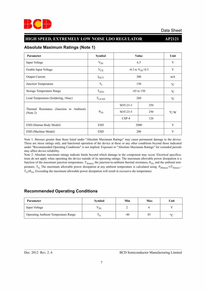
Parameter Symbol Value Unit
Input Voltage VIN 6.5 V
Enable Input Voltage VCE -0.3 to VIN+0.3 V
Output Current IOUT 300 mA
Junction Temperature TJ 150 oC
Storage Temperature Range TSTG -65 to 150 oC
Lead Temperature (Soldering, 10sec) TLEAD 260 oC
Thermal Resistance (Junction to Ambient)(Note 2) θJA
SOT-23-3 250
oC/WSOT-23-5 250
CSP-4 126
ESD (Human Body Model) ESD 2000 V
ESD (Machine Model) ESD 200 V
Absolute Maximum Ratings (Note 1)
Parameter Symbol Min Max Unit
Input Voltage VIN 2 6 V
Operating Ambient Temperature Range TA -40 85 oC
Recommended Operating Conditions
Note 1: Stresses greater than those listed under "Absolute Maximum Ratings" may cause permanent damage to the device.These are stress ratings only, and functional operation of the device at these or any other conditions beyond those indicatedunder "Recommended Operating Conditions" is not implied. Exposure to "Absolute Maximum Ratings" for extended periodsmay affect device reliability.Note 2: Absolute maximum ratings indicate limits beyond which damage to the component may occur. Electrical specifica-tions do not apply when operating the device outside of its operating ratings. The maximum allowable power dissipation is afunction of the maximum junction temperature, TJ(max), the junction-to-ambient thermal resistance, θJA, and the ambient tem-perature, TA. The maximum allowable power dissipation at any ambient temperature is calculated using: PD(max)=(TJ(max) -TA)/θJA. Exceeding the maximum allowable power dissipation will result in excessive die temperature.

Data Sheet
8
Dec. 2012 Rev. 2. 6 BCD Semiconductor Manufacturing Limited
HIGH SPEED, EXTREMELY LOW NOISE LDO REGULATOR AP2121
Electrical Characteristics
Parameter Symbol Conditions Min Typ Max Unit
Output Voltage VOUTVIN=2.2V1mA≤IOUT≤30mA
1.176 1.2 1.224 V
Input Voltage VIN 6 V
Output Current IOUT VIN-VOUT=1V 200 mA
Load Regulation VRLOADVIN=2.2V1mA≤IOUT≤80mA
12 40 mV
Line Regulation VRLINE2.2V≤VIN≤6VIOUT=30mA
4 16 mV
Dropout Voltage VDROP
IOUT=10mA 700 900
mVIOUT=100mA 700 900
IOUT=150mA 700 900
IOUT=200mA 700 900
Quiescent Current IQ VIN=2.2V, IOUT=0mA 25 50 μA
Standby Current ISTDVIN=2.2VVCE in OFF mode
0.1 1 μA
Power Supply Rejection Ratio PSRR
Ripple 0.5Vp-p, f=1kHz VIN=2.2V 70 dB
Output Voltage Temperature Coefficient
ΔVOUT/ΔTIOUT=30mA
±120 μV/oC
(ΔVOUT/VOUT)/ΔT ±100 ppm/oC
Short Current Limit ILIMIT VOUT=0V 50 mA
RMS Output Noise VNOISETA=25oC10Hz ≤f≤100kHz
30 μVrms
CE "High" Voltage CE input voltage "High" 1.5 V
CE "Low" Voltage CE input voltage "Low" 0.25 V
CE Pull-down Resistance RPD 2.5 5 10 MΩ
Thermal Resistance(Junction to Case)
θJC
SOT-23-3 74oC/WSOT-23-5 74
CSP-4 5
(VIN=2.2V, TJ=25oC, CIN=1μF, COUT=1μF, Bold typeface applies over -40oC≤TJ≤85oC, unless otherwise specified.)
AP2121-1.2 Electrical Characteristics

9
Dec. 2012 Rev. 2. 6 BCD Semiconductor Manufacturing Limited
HIGH SPEED, EXTREMELY LOW NOISE LDO REGULATOR AP2121
Data Sheet
Parameter Symbol Conditions Min Typ Max Unit
Output Voltage VOUTVIN=2.3V1mA≤IOUT≤30mA
1.274 1.3 1.326 V
Input Voltage VIN 6 V
Output Current IOUT VIN-VOUT=1V 200 mA
Load Regulation VRLOADVIN=2.3V1mA≤IOUT≤80mA
12 40 mV
Line Regulation VRLINE2.3V≤VIN≤6VIOUT=30mA
4 16 mV
Dropout Voltage VDROP
IOUT=10mA 600 800
mVIOUT=100mA 600 800
IOUT=150mA 600 800
IOUT=200mA 600 800
Quiescent Current IQ VIN=2.3V, IOUT=0mA 25 50 μA
Standby Current ISTDVIN=2.3VVCE in OFF mode
0.1 1 μA
Power Supply Rejection Ratio PSRR
Ripple 0.5Vp-p, f=1kHz VIN=2.3V 70 dB
Output Voltage Temperature Coefficient
ΔVOUT/ΔTIOUT=30mA
±130 μV/oC
(ΔVOUT/VOUT)/ΔT ±100 ppm/oC
Short Current Limit ILIMIT VOUT=0V 50 mA
RMS Output Noise VNOISETA=25oC10Hz ≤f≤100kHz
30 μVrms
CE "High" Voltage CE input voltage "High" 1.5 V
CE "Low" Voltage CE input voltage "Low" 0.25 V
CE Pull-down Resistance RPD 2.5 5 10 MΩ
Thermal Resistance(Junction to Case)
θJC
SOT-23-3 74oC/WSOT-23-5 74
CSP-4 5
(VIN=2.3V, TJ=25oC, CIN=1μF, COUT=1μF, Bold typeface applies over -40oC≤TJ≤85oC, unless otherwise specified.)
Electrical Characteristics (Continued)AP2121-1.3 Electrical Characteristics
Data Sheet
10
Dec. 2012 Rev. 2. 6 BCD Semiconductor Manufacturing Limited
HIGH SPEED, EXTREMELY LOW NOISE LDO REGULATOR AP2121
Parameter Symbol Conditions Min Typ Max Unit
Output Voltage VOUTVIN=2.5V1mA≤IOUT≤30mA
1.47 1.5 1.53 V
Input Voltage VIN 6 V
Output Current IOUT VIN-VOUT=1V 200 mA
Load Regulation VRLOADVIN=2.5V1mA≤IOUT≤80mA
12 40 mV
Line Regulation VRLINE2.3V≤VIN≤6VIOUT=30mA
4 16 mV
Dropout Voltage VDROP
IOUT=10mA 400 600
mVIOUT=100mA 400 600
IOUT=150mA 400 600
IOUT=200mA 400 600
Quiescent Current IQ VIN=2.5V, IOUT=0mA 25 50 μA
Standby Current ISTDVIN=2.5VVCE in OFF mode
0.1 1 μA
Power Supply Rejection Ratio PSRR
Ripple 0.5Vp-p, f=1kHz VIN=2.5V 70 dB
Output Voltage Temperature Coefficient
ΔVOUT/ΔTIOUT=30mA
±150 μV/oC
(ΔVOUT/VOUT)/ΔT ±100 ppm/oC
Short Current Limit ILIMIT VOUT=0V 50 mA
RMS Output Noise VNOISETA=25oC10Hz ≤f≤100kHz
30 μVrms
CE "High" Voltage CE input voltage "High" 1.5 V
CE "Low" Voltage CE input voltage "Low" 0.25 V
CE Pull-down Resistance RPD 2.5 5 10 MΩ
Thermal Resistance(Junction to Case)
θJC
SOT-23-3 74oC/WSOT-23-5 74
CSP-4 5
(VIN=2.5V, TJ=25oC, CIN=1μF, COUT=1μF, Bold typeface applies over -40oC≤TJ≤85oC, unless otherwise specified.)
AP2121-1.5 Electrical CharacteristicsElectrical Characteristics (Continued)

11
Dec. 2012 Rev. 2. 6 BCD Semiconductor Manufacturing Limited
HIGH SPEED, EXTREMELY LOW NOISE LDO REGULATOR AP2121
Data Sheet
Parameter Symbol Conditions Min Typ Max Unit
Output Voltage VOUTVIN=2.8V1mA≤IOUT≤30mA
1.764 1.8 1.836 V
Input Voltage VIN 6 V
Output Current IOUT VIN-VOUT=1V 200 mA
Load Regulation VRLOADVIN=2.8V1mA≤IOUT≤80mA
12 40 mV
Line Regulation VRLINE2.3V≤VIN≤6VIOUT=30mA
4 16 mV
Dropout Voltage VDROP
IOUT=10mA 20 40
mVIOUT=100mA 150 300
IOUT=150mA 200 400
IOUT=200mA 250 500
Quiescent Current IQ VIN=2.8V, IOUT=0mA 25 50 μA
Standby Current ISTDVIN=2.8VVCE in OFF mode
0.1 1 μA
Power Supply Rejection Ratio PSRR
Ripple 0.5Vp-p, f=1kHz VIN=2.8V 70 dB
Output Voltage Temperature Coefficient
ΔVOUT/ΔTIOUT=30mA
±180 μV/oC
(ΔVOUT/VOUT)/ΔT ±100 ppm/oC
Short Current Limit ILIMIT VOUT=0V 50 mA
RMS Output Noise VNOISETA=25oC10Hz ≤f≤100kHz
30 μVrms
CE "High" Voltage CE input voltage "High" 1.5 V
CE "Low" Voltage CE input voltage "Low" 0.25 V
CE Pull-down Resistance RPD 2.5 5 10 MΩ
Thermal Resistance(Junction to Case)
θJC
SOT-23-3 74oC/WSOT-23-5 74
CSP-4 5
(VIN=2.8V, TJ=25oC, CIN=1μF, COUT=1μF, Bold typeface applies over -40oC≤TJ≤85oC, unless otherwise specified.)
Electrical Characteristics (Continued)AP2121-1.8 Electrical Characteristics

Data Sheet
12
Dec. 2012 Rev. 2. 6 BCD Semiconductor Manufacturing Limited
HIGH SPEED, EXTREMELY LOW NOISE LDO REGULATOR AP2121
Electrical Characteristics (Continued)
Parameter Symbol Conditions Min Typ Max Unit
Output Voltage VOUTVIN=3.5V1mA≤IOUT≤30mA
2.45 2.5 2.55 V
Input Voltage VIN 6 V
Output Current IOUT VIN-VOUT=1V 200 mA
Load Regulation VRLOADVIN=3.5V1mA≤IOUT≤80mA
12 40 mV
Line Regulation VRLINE3V≤VIN≤6VIOUT=30mA
4 16 mV
Dropout Voltage VDROP
IOUT=10mA 20 40
mVIOUT=100mA 150 300
IOUT=150mA 200 400
IOUT=200mA 250 500
Quiescent Current IQ VIN=3.5V, IOUT=0mA 25 50 μA
Standby Current ISTDVIN=3.5VVCE in OFF mode
0.1 1 μA
Power Supply Rejection Ratio PSRR
Ripple 0.5Vp-p, f=1kHz VIN=3.5V 70 dB
Output Voltage Temperature Coefficient
ΔVOUT/ΔTIOUT=30mA
±250 μV/oC
(ΔVOUT/VOUT)/ΔT ±100 ppm/oC
Short Current Limit ILIMIT VOUT=0V 50 mA
RMS Output Noise VNOISETA=25oC10Hz ≤f≤100kHz
30 μVrms
CE "High" Voltage CE input voltage "High" 1.5 V
CE "Low" Voltage CE input voltage "Low" 0.25 V
CE Pull-down Resistance RPD 2.5 5 10 MΩ
Thermal Resistance(Junction to Case)
θJC
SOT-23-3 74oC/WSOT-23-5 74
CSP-4 5
(VIN=3.5V, TJ=25oC, CIN=1μF, COUT=1μF, Bold typeface applies over -40oC≤TJ≤85oC, unless otherwise specified.)
AP2121-2.5 Electrical Characteristics

13
Dec. 2012 Rev. 2. 6 BCD Semiconductor Manufacturing Limited
HIGH SPEED, EXTREMELY LOW NOISE LDO REGULATOR AP2121
Data Sheet
Parameter Symbol Conditions Min Typ Max Unit
Output Voltage VOUTVIN=3.8V1mA≤IOUT≤30mA
2.744 2.8 2.856 V
Input Voltage VIN 6 V
Output Current IOUT VIN-VOUT=1V 200 mA
Load Regulation VRLOADVIN=3.8V1mA≤IOUT≤80mA
12 40 mV
Line Regulation VRLINE3.3V≤VIN≤6VIOUT=30mA
4 16 mV
Dropout Voltage VDROP
IOUT=10mA 20 40
mVIOUT=100mA 150 300
IOUT=150mA 200 400
IOUT=200mA 250 500
Quiescent Current IQ VIN=3.8V, IOUT=0mA 25 50 μA
Standby Current ISTDVIN=3.8VVCE in OFF mode
0.1 1 μA
Power Supply Rejection Ratio PSRR
Ripple 0.5Vp-p, f=1kHz VIN=3.8V 70 dB
Output Voltage Temperature Coefficient
ΔVOUT/ΔTIOUT=30mA
±280 μV/oC
(ΔVOUT/VOUT)/ΔT ±100 ppm/oC
Short Current Limit ILIMIT VOUT=0V 50 mA
RMS Output Noise VNOISETA=25oC10Hz ≤f≤100kHz
30 μVrms
CE "High" Voltage CE input voltage "High" 1.5 V
CE "Low" Voltage CE input voltage "Low" 0.25 V
CE Pull-down Resistance RPD 2.5 5 10 MΩ
Thermal Resistance(Junction to Case)
θJC
SOT-23-3 74oC/WSOT-23-5 74
CSP-4 5
(VIN=3.8V, TJ=25oC, CIN=1μF, COUT=1μF, Bold typeface applies over -40oC≤TJ≤85oC, unless otherwise specified.)
Electrical Characteristics (Continued)AP2121-2.8 Electrical Characteristics

Data Sheet
14
Dec. 2012 Rev. 2. 6 BCD Semiconductor Manufacturing Limited
HIGH SPEED, EXTREMELY LOW NOISE LDO REGULATOR AP2121
Parameter Symbol Conditions Min Typ Max Unit
Output Voltage VOUTVIN=3.85V1mA≤IOUT≤30mA
2.793 2.85 2.907 V
Input Voltage VIN 6 V
Output Current IOUT VIN-VOUT=1V 200 mA
Load Regulation VRLOADVIN=3.85V1mA≤IOUT≤80mA
12 40 mV
Line Regulation VRLINE3.3V≤VIN≤6VIOUT=30mA
4 16 mV
Dropout Voltage VDROP
IOUT=10mA 20 40
mVIOUT=100mA 150 300
IOUT=150mA 200 400
IOUT=200mA 250 500
Quiescent Current IQ VIN=3.85V, IOUT=0mA 25 50 μA
Standby Current ISTDVIN=3.85VVCE in OFF mode
0.1 1 μA
Power Supply Rejection Ratio PSRR
Ripple 0.5Vp-p, f=1kHz VIN=3.85V 70 dB
Output Voltage Temperature Coefficient
ΔVOUT/ΔTIOUT=30mA
±280 μV/oC
(ΔVOUT/VOUT)/ΔT ±100 ppm/oC
Short Current Limit ILIMIT VOUT=0V 50 mA
RMS Output Noise VNOISETA=25oC10Hz ≤f≤100kHz
30 μVrms
CE "High" Voltage CE input voltage "High" 1.5 V
CE "Low" Voltage CE input voltage "Low" 0.25 V
CE Pull-down Resistance RPD 2.5 5 10 MΩ
Thermal Resistance(Junction to Case)
θJCCSP-4 5 oC/W
(VIN=3.85V, TJ=25oC, CIN=1μF, COUT=1μF, Bold typeface applies over -40oC≤TJ≤85oC, unless otherwise specified.)
Electrical Characteristics (Continued)AP2121-2.85 Electrical Characteristics

15
Dec. 2012 Rev. 2. 6 BCD Semiconductor Manufacturing Limited
HIGH SPEED, EXTREMELY LOW NOISE LDO REGULATOR AP2121
Data Sheet
Parameter Symbol Conditions Min Typ Max Unit
Output Voltage VOUTVIN=4V1mA≤IOUT≤30mA
2.94 3.0 3.06 V
Input Voltage VIN 6 V
Output Current IOUT VIN-VOUT=1V 200 mA
Load Regulation VRLOADVIN=4V1mA≤IOUT≤80mA 12 40 mV
Line Regulation VRLINE3.5V≤VIN≤6VIOUT=30mA 4 16 mV
Dropout Voltage VDROP
IOUT=10mA 20 40
mVIOUT=100mA 150 300
IOUT=150mA 200 400
IOUT=200mA 250 500
Quiescent Current IQ VIN=4V, IOUT=0mA 25 50 μA
Standby Current ISTDVIN=4VVCE in OFF mode
0.1 1 μA
Power Supply Rejection Ratio PSRR
Ripple 0.5Vp-p, f=1kHzVIN=4V 70 dB
Output Voltage Temperature Coefficient
ΔVOUT/ΔTIOUT=30mA
±300 μV/oC
(ΔVOUT/VOUT)/ΔT ±100 ppm/oC
Short Current Limit ILIMIT VOUT=0V 50 mA
RMS Output Noise VNOISETA=25oC10Hz ≤f≤100kHz
30 μVrms
CE "High" Voltage CE input voltage "High" 1.5 V
CE "Low" Voltage CE input voltage "Low" 0.25 V
CE Pull-down Resistance RPD 2.5 5 10 MΩ
Thermal Resistance(Junction to Case)
θJC
SOT-23-3 74oC/WSOT-23-5 74
CSP-4 5
(VIN=4V, TJ=25oC, CIN=1μF, COUT=1μF, Bold typeface applies over -40oC≤TJ≤85oC, unless otherwise specified.)
Electrical Characteristics (Continued)AP2121-3.0 Electrical Characteristics

Data Sheet
16
Dec. 2012 Rev. 2. 6 BCD Semiconductor Manufacturing Limited
HIGH SPEED, EXTREMELY LOW NOISE LDO REGULATOR AP2121
Electrical Characteristics (Continued)
Parameter Symbol Conditions Min Typ Max Unit
Output Voltage VOUTVIN=4.2V1mA≤IOUT≤30mA
3.136 3.2 3.264 V
Input Voltage VIN 6 V
Output Current IOUT VIN-VOUT=1V 200 mA
Load Regulation VRLOADVIN=4.2V1mA≤ IOUT≤ 80mA
12 40 mV
Line Regulation VRLINE3.7V≤VIN≤6VIOUT=30mA
4 16 mV
Dropout Voltage VDROP
IOUT=10mA 20 40
mVIOUT=100mA 150 300
IOUT=150mA 200 400
IOUT=200mA 250 500
Quiescent Current IQ VIN=4.2V, IOUT=0mA 25 50 μA
Standby Current ISTDVIN=4.2VVCE in OFF mode
0.1 1 μA
Power Supply Rejection Ratio PSRR
Ripple 0.5Vp-p, f=1kHz VIN=4.2V 70 dB
Output Voltage Temperature Coefficient
ΔVOUT/ΔTIOUT=30mA
±320 μV/oC
(ΔVOUT/VOUT)/ΔT ±100 ppm/oC
Short Current Limit ILIMIT VOUT=0V 50 mA
RMS Output Noise VNOISETA=25oC10Hz ≤f≤100kHz
30 μVrms
CE "High" Voltage CE input voltage "High" 1.5 V
CE "Low" Voltage CE input voltage "Low" 0.25 V
CE Pull-down Resistance RPD 2.5 5 10 MΩ
Thermal Resistance(Junction to Case)
θJC
SOT-23-3 74oC/WSOT-23-5 74
CSP-4 5
(VIN=4.2V, TJ=25oC, CIN=1μF, COUT=1μF, Bold typeface applies over -40oC≤TJ≤85oC, unless otherwise specified.)
AP2121-3.2 Electrical Characteristics
17
Dec. 2012 Rev. 2. 6 BCD Semiconductor Manufacturing Limited
HIGH SPEED, EXTREMELY LOW NOISE LDO REGULATOR AP2121
Data Sheet
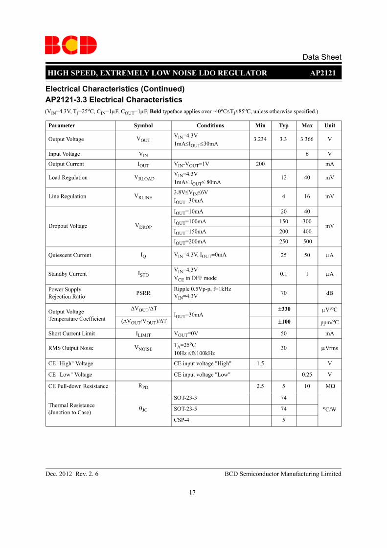
Parameter Symbol Conditions Min Typ Max Unit
Output Voltage VOUTVIN=4.3V1mA≤IOUT≤30mA
3.234 3.3 3.366 V
Input Voltage VIN 6 V
Output Current IOUT VIN-VOUT=1V 200 mA
Load Regulation VRLOADVIN=4.3V1mA≤ IOUT≤ 80mA
12 40 mV
Line Regulation VRLINE3.8V≤VIN≤6VIOUT=30mA
4 16 mV
Dropout Voltage VDROP
IOUT=10mA 20 40
mVIOUT=100mA 150 300
IOUT=150mA 200 400
IOUT=200mA 250 500
Quiescent Current IQ VIN=4.3V, IOUT=0mA 25 50 μA
Standby Current ISTDVIN=4.3VVCE in OFF mode
0.1 1 μA
Power Supply Rejection Ratio PSRR
Ripple 0.5Vp-p, f=1kHz VIN=4.3V 70 dB
Output Voltage Temperature Coefficient
ΔVOUT/ΔTIOUT=30mA
±330 μV/oC
(ΔVOUT/VOUT)/ΔT ±100 ppm/oC
Short Current Limit ILIMIT VOUT=0V 50 mA
RMS Output Noise VNOISETA=25oC10Hz ≤f≤100kHz
30 μVrms
CE "High" Voltage CE input voltage "High" 1.5 V
CE "Low" Voltage CE input voltage "Low" 0.25 V
CE Pull-down Resistance RPD 2.5 5 10 MΩ
Thermal Resistance(Junction to Case)
θJC
SOT-23-3 74oC/WSOT-23-5 74
CSP-4 5
(VIN=4.3V, TJ=25oC, CIN=1μF, COUT=1μF, Bold typeface applies over -40oC≤TJ≤85oC, unless otherwise specified.)
AP2121-3.3 Electrical CharacteristicsElectrical Characteristics (Continued)

Data Sheet
18
Dec. 2012 Rev. 2. 6 BCD Semiconductor Manufacturing Limited
HIGH SPEED, EXTREMELY LOW NOISE LDO REGULATOR AP2121
Typical Performance Characteristics
Figure 4. Output Voltage vs. Output Current
Figure 6. Output Voltage vs. Output Current
Figure 5. Output Voltage vs. Output Current
Figure 7. Output Voltage vs. Output Current
0 50 100 150 200 250 300 3500.0
0.2
0.4
0.6
0.8
1.0
1.2
1.4
Out
put V
olta
ge (V
)
Output Current (mA)
AP2121-1.2 VIN=2V VIN=2.5V V
IN=3V
0 50 100 150 200 250 300 350 4000.0
0.2
0.4
0.6
0.8
1.0
1.2
1.4
1.6
1.8
AP2121-1.5 VIN= 2V VIN= 2.5V VIN= 4V
Out
put V
olta
ge (V
)
Output Current (mA)
0 50 100 150 200 250 300 3500.0
0.2
0.4
0.6
0.8
1.0
1.2
1.4
1.6
1.8
2.0
Out
put V
olta
ge (V
)
Output Current (mA)
AP2121-1.8 VIN= 2.2V VIN= 2.8V VIN= 4V
0 50 100 150 200 250 300 3500.0
0.4
0.8
1.2
1.6
2.0
2.4
2.8
AP2121-2.5 VIN= 2.8V VIN= 3.5V VIN= 5V
Out
put V
olta
ge (V
)
Output Current (mA)

19
Dec. 2012 Rev. 2. 6 BCD Semiconductor Manufacturing Limited
HIGH SPEED, EXTREMELY LOW NOISE LDO REGULATOR AP2121
Data Sheet
Typical Performance Characteristics (Continued)
Figure 9. Output Voltage vs. Input Voltage
0 1 2 3 4 5 6 72.00
2.25
2.50
2.75
3.00
3.25
3.50
Out
put V
olta
ge (V
)
Input Voltage (V)
AP2121-3.0 IOUT=30mA
Figure 10. Output Voltage vs. Input Voltage
0 1 2 3 4 5 6 70.0
0.2
0.4
0.6
0.8
1.0
1.2
1.4
Out
put V
olta
ge (V
)
Input Voltage (V)
AP2121-1.2IOUT
=30mA
Figure 8. Output Voltage vs. Output Current
Figure 11. Dropout Voltage vs. Output Current
0 40 80 120 160 2000.0
0.1
0.2
0.3
0.4
0.5
0.6
Minimum Operating Requirement
Dro
pout
Vol
tage
(V)
Output Current (mA)
AP2121-1.2
0 50 100 150 200 250 300 3500.0
0.5
1.0
1.5
2.0
2.5
3.0
3.5
Out
put V
olta
ge (V
)
Output Current (mA)
AP2121-3.0 VIN=3.3V VIN=4V V
IN=6V

Data Sheet
20
Dec. 2012 Rev. 2. 6 BCD Semiconductor Manufacturing Limited
HIGH SPEED, EXTREMELY LOW NOISE LDO REGULATOR AP2121
Typical Performance Characteristics (Continued)
Figure 13. Output Voltage vs. Junction Temperature
0 40 80 120 160 2000.0
0.1
0.2
0.3
0.4
0.5
0.6
Dro
pout
Vol
tage
(V)
Output Current (mA)
AP2121-3.0
Figure 12. Dropout Voltage vs. Output Current
-25 0 25 50 75 100 1252.90
2.92
2.94
2.96
2.98
3.00
3.02
3.04
3.06
3.08
3.10
AP2121-3.0V
IN=4V
IOUT=30mA
Out
put V
olta
ge (V
)
Junction Temperature (oC)
Figure 14. Output Voltage vs. Junction Temperature
-25 0 25 50 75 100 1251.190
1.192
1.194
1.196
1.198
1.200
1.202
1.204
1.206
1.208
1.210
Out
put V
olta
ge (V
)
Junction Temperature (oC)
AP2121-1.2VIN=2.2VIOUT
=30mA
Figure 15. Supply Current vs. Input Voltage
0 1 2 3 4 5 6 70
5
10
15
20
25
30
Supp
ly C
urre
nt (μ
A)
Input Voltage (V)
AP2121-1.2IOUT=0mA

21
Dec. 2012 Rev. 2. 6 BCD Semiconductor Manufacturing Limited
HIGH SPEED, EXTREMELY LOW NOISE LDO REGULATOR AP2121
Data Sheet
Typical Performance Characteristics (Continued)
Figure 17. Supply Current vs. Junction Temperature
0 1 2 3 4 5 6 70
10
20
30
40
50
60
Sup
ply
Cur
rent
(μA
)
Input Voltage (V)
AP2121-3.0 IOUT=0mA
Figure 16. Supply Current vs. Input Voltage
-25 0 25 50 75 100 1250
5
10
15
20
25
30
35
40
Supp
ly C
urre
nt (μ
A)
Junction Temperature (oC)
AP2121-3.0 VIN=4V IOUT=0mA
Figure 18. Supply Current vs. Junction Temperature
-25 0 25 50 75 100 1250
5
10
15
20
25
30
35
40
Sup
ply
Cur
rent
(μA
)
Junction Temperature (oC)
AP2121-1.2VIN=2.2V IOUT=0mA
Figure 19. Line Transient (Conditions: IOUT=30mA, CIN=1μF, COUT=1μF)
ΔVO
UT
(0.0
5V/D
iv)
VIN
(1V/
Div
)
Time (100μs/Div)
AP2121-1.2
0
2.2
3.2
0.05
-0.05
4.2

Data Sheet
22
Dec. 2012 Rev. 2. 6 BCD Semiconductor Manufacturing Limited
HIGH SPEED, EXTREMELY LOW NOISE LDO REGULATOR AP2121
Typical Performance Characteristics (Continued)
Figure 21. Load Transient (Conditions: VIN=2.2V, CIN=1μF, COUT=1μF)
V OU
T (0
.1V/
Div
)
Time (200μs/Div)
AP2121-1.2
1.2
1.1
AP2121-3.0
Figure 20. Line Transient (Conditions: IOUT=30mA, CIN=1μF, COUT=1μF)
AP2121-3.0
Time (200μs/Div)
Figure 22. Load Transient (Conditions: VIN=4V, CIN=1μF, COUT=1μF)
Time (20μs/Div)
ΔVO
UT
(0.0
5V/D
iv)
V IN
(1V
/Div
)
0
4
5
0.05
-0.05
6 1.3
I OU
T (1
00m
A/D
iv)
0
200
3.0
2.9
3.1
100
VO
UT
(0.1
V/D
iv)
I OU
T (1
00m
A/D
iv)
0
200
100
Figure 23. PSRR vs. Frequency
10 100 1k 10k 100k0
10
20
30
40
50
60
70
80
90
100
PSR
R (d
B)
Frequency (Hz)
AP2121-1.2VIN=2.2VIOUT=30mACIN=COUT=1μF

23
Dec. 2012 Rev. 2. 6 BCD Semiconductor Manufacturing Limited
HIGH SPEED, EXTREMELY LOW NOISE LDO REGULATOR AP2121
Data Sheet
10 100 1k 10k 100k0
10
20
30
40
50
60
70
80
90
100
PS
RR
(dB
)
Frequency (Hz)
AP2121-3.0VIN=4VIOUT=30mACIN=COUT=1μF
Typical Performance Characteristics (Continued)
Figure 24. PSRR vs. Frequency

Data Sheet
24
Dec. 2012 Rev. 2. 6 BCD Semiconductor Manufacturing Limited
HIGH SPEED, EXTREMELY LOW NOISE LDO REGULATOR AP2121
Typical Application
Figure 25. Typical Application of AP2121
Note: Filter capacitors are required at the AP2121's input and output. 1μF capacitor is required at the input. Theminimum output capacitance required for stability should be more than 1μF with ESR from 0.01Ω to 100Ω.Ceramic capacitors are recommended.
VIN
AP2121-1.2
CIN
1μF
COUT
1μF
VOUTVIN VOUT
GND
VIN
AP2121-3.0
CIN
1μF
COUT
1μF
VOUTVIN VOUT
GND
CE NC
VIN=2.2V VOUT=1.2V
VOUT=3VVIN=4V
25
Dec. 2012 Rev. 2. 6 BCD Semiconductor Manufacturing Limited
HIGH SPEED, EXTREMELY LOW NOISE LDO REGULATOR AP2121
Data Sheet
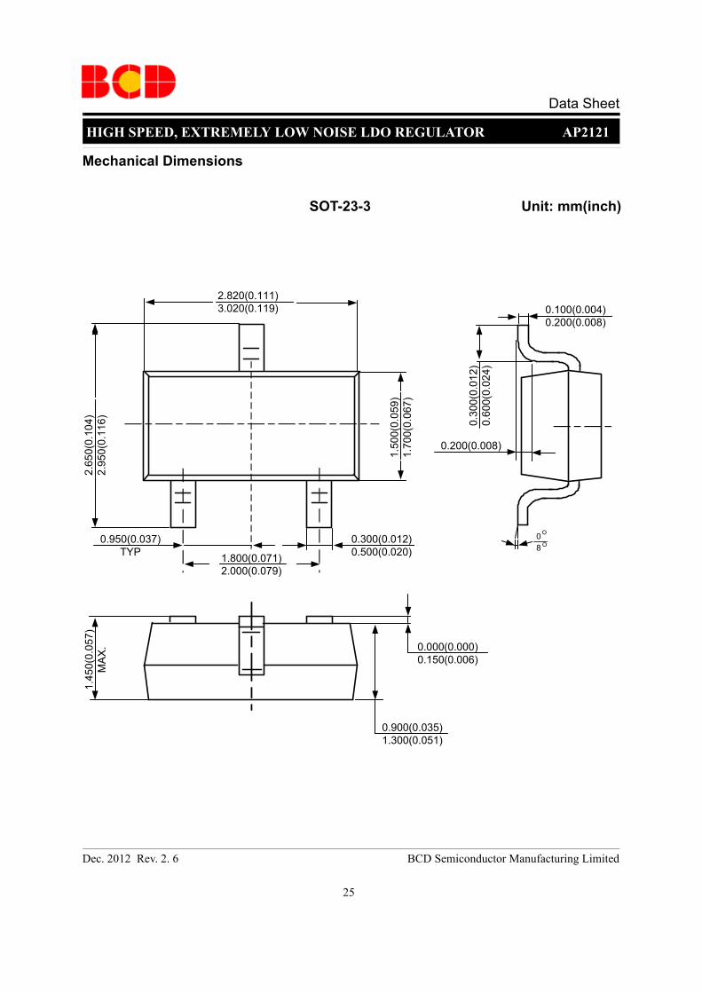
Mechanical Dimensions
SOT-23-3 Unit: mm(inch)
2.820(0.111)3.020(0.119)
2.65
0(0.
104)
2.95
0(0.
116)
0.950(0.037)TYP
0.300(0.012)0.500(0.020)
1.50
0(0.
059)
1.70
0(0.
067)
1.800(0.071)2.000(0.079)
0.30
0(0.
012)
0.60
0(0.
024)
0.100(0.004)0.200(0.008)
0.000(0.000)0.150(0.006)
0.900(0.035)1.300(0.051)
1.45
0(0.
057)
MA
X.
0.200(0.008)
08 °°

Data Sheet
26
Dec. 2012 Rev. 2. 6 BCD Semiconductor Manufacturing Limited
HIGH SPEED, EXTREMELY LOW NOISE LDO REGULATOR AP2121
Mechanical Dimensions (Continued)
SOT-23-5 Unit: mm(inch)
2.820(0.111)
2.65
0(0 .
104)
1.50
0(0.
0 59)
0.000(0.000)
0.300(0.012)0.950(0.037)
0.900(0.035)
0.100(0.004)
0.200(0.008)
0.30
0(0.
012)
8°0°
3.020(0.119)
1.70
0(0.
067)
2.95
0(0.
116)
0.400(0.016)
0.150(0.006)
1.300(0.051)
0.200(0.008)
0.60
0(0.
024)
1.800(0.071)2.000(0.079)
0.700(0.028)REF
TYP
1.45
0(0.
057)
MA X
27
Dec. 2012 Rev. 2. 6 BCD Semiconductor Manufacturing Limited
HIGH SPEED, EXTREMELY LOW NOISE LDO REGULATOR AP2121
Data Sheet
Mechanical Dimensions (Continued)
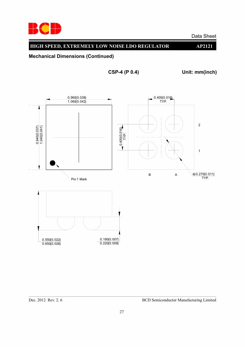
CSP-4 (P 0.4) Unit: mm(inch)
0.960(0.038)1.060(0.042)
Pin 1 Mark
0.94
0(0.
037)
1.04
0(0.
041)
0.400(0.016)TYP.
0.40
0(0.
016)
TYP.
Φ0.270(0.011)TYP.
B A
1
2
0.550(0.022)0.650(0.026)
0.180(0.007)0.220(0.009)
Data Sheet
28
Dec. 2012 Rev. 2. 6 BCD Semiconductor Manufacturing Limited
HIGH SPEED, EXTREMELY LOW NOISE LDO REGULATOR AP2121
Mechanical Dimensions (Continued)
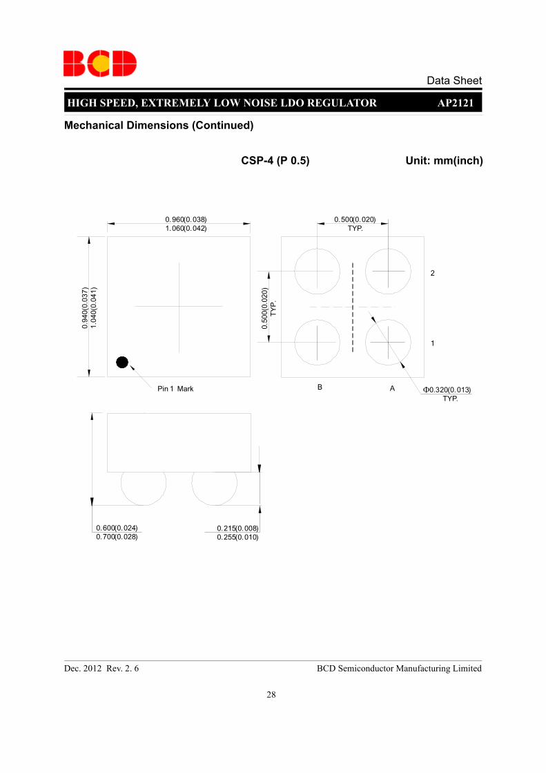
CSP-4 (P 0.5) Unit: mm(inch)
0.960(0.038)1.060(0.042)
0.94
0(0.
037)
1.04
0(0.
041)
0.500(0.020)TYP.
0.50
0(0.
020)
TYP.
Φ0.320(0.013)TYP.
Pin 1 Mark
0.600(0.024)0.700(0.028)
0.215(0.008)0.255(0.010)
B A
1
2

IMPORTANT NOTICE
BCD Semiconductor Manufacturing Limited reserves the right to make changes without further notice to any products or specifi-cations herein. BCD Semiconductor Manufacturing Limited does not assume any responsibility for use of any its products for anyparticular purpose, nor does BCD Semiconductor Manufacturing Limited assume any liability arising out of the application or useof any its products or circuits. BCD Semiconductor Manufacturing Limited does not convey any license under its patent rights orother rights nor the rights of others.
- Wafer FabShanghai SIM-BCD Semiconductor Manufacturing Limited800, Yi Shan Road, Shanghai 200233, ChinaTel: +86-21-6485 1491, Fax: +86-21-5450 0008
BCD Semiconductor Manufacturing LimitedMAIN SITE
REGIONAL SALES OFFICEShenzhen OfficeShanghai SIM-BCD Semiconductor Manufacturing Co., Ltd. Shenzhen OfficeAdvanced Analog Circuits (Shanghai) Corporation Shenzhen OfficeRoom E, 5F, Noble Center, No.1006, 3rd Fuzhong Road, Futian District, Shenzhen 518026, China Tel: +86-755-8826 7951Fax: +86-755-8826 7865
Taiwan OfficeBCD Semiconductor (Taiwan) Company Limited4F, 298-1, Rui Guang Road, Nei-Hu District, Taipei, TaiwanTel: +886-2-2656 2808Fax: +886-2-2656 2806
USA OfficeBCD Semiconductor Corporation30920 Huntwood Ave. Hayward,CA 94544, U.S.ATel : +1-510-324-2988Fax: +1-510-324-2788
- IC Design GroupAdvanced Analog Circuits (Shanghai) Corporation8F, Zone B, 900, Yi Shan Road, Shanghai 200233, ChinaTel: +86-21-6495 9539, Fax: +86-21-6485 9673
BCD Semiconductor Manufacturing Limited
http://www.bcdsemi.com
BCD Semiconductor Manufacturing Limited
IMPORTANT NOTICE
BCD Semiconductor Manufacturing Limited reserves the right to make changes without further notice to any products or specifi-cations herein. BCD Semiconductor Manufacturing Limited does not assume any responsibility for use of any its products for anyparticular purpose, nor does BCD Semiconductor Manufacturing Limited assume any liability arising out of the application or useof any its products or circuits. BCD Semiconductor Manufacturing Limited does not convey any license under its patent rights orother rights nor the rights of others.
- Wafer FabShanghai SIM-BCD Semiconductor Manufacturing Co., Ltd.800 Yi Shan Road, Shanghai 200233, ChinaTel: +86-21-6485 1491, Fax: +86-21-5450 0008
MAIN SITE
REGIONAL SALES OFFICEShenzhen OfficeShanghai SIM-BCD Semiconductor Manufacturing Co., Ltd., Shenzhen OfficeUnit A Room 1203, Skyworth Bldg., Gaoxin Ave.1.S., Nanshan District, Shenzhen,China Tel: +86-755-8826 7951Fax: +86-755-8826 7865
Taiwan OfficeBCD Semiconductor (Taiwan) Company Limited4F, 298-1, Rui Guang Road, Nei-Hu District, Taipei, TaiwanTel: +886-2-2656 2808Fax: +886-2-2656 2806
USA OfficeBCD Semiconductor Corp.30920 Huntwood Ave. Hayward,CA 94544, USATel : +1-510-324-2988Fax: +1-510-324-2788
- HeadquartersBCD Semiconductor Manufacturing LimitedNo. 1600, Zi Xing Road, Shanghai ZiZhu Science-based Industrial Park, 200241, ChinaTel: +86-21-24162266, Fax: +86-21-24162277