P6000A/P5000- Output Options Isolated Parallel BCD Dual 8 ... CD/newport/PDF/P6000A_O.pdf · *BOARD...
32
P6000A/P5000 Output Options Operator’s Manual NEWPORT Electronics, Inc.
Transcript of P6000A/P5000- Output Options Isolated Parallel BCD Dual 8 ... CD/newport/PDF/P6000A_O.pdf · *BOARD...
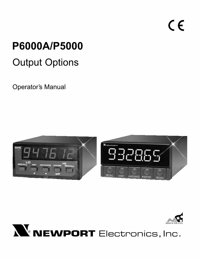
P6000A/P5000
Output Options
Operator’s Manual
NEWPORT Electronics,Inc.

CountersFrequency Meters
PID ControllersClock/Timers
PrintersProcess Meters
On/OffControllersRecordersRelativeHumidity
TransmittersThermocouples
ThermistorsWire
Rate MetersTimers
TotalizersStrain Gauge
MetersVoltmetersMultimeters
Soldering IronTesterspH pens
pH ControllerspH Electrodes
RTDsThermowellsFlow Sensors
For Immediate AssistanceIn the U.S.A. and Canada: 1-800-NEWPORT®
In Mexico: (95) 800-NEWPORTSM
Or call your local NEWPORT Office.
It is the policy of NEWPORT to comply with all worldwide safety and EMC/EMI regulations that apply. NEWPORT is constantly pursuingcertification of its products to the European New Approach Directives. NEWPORT will add the CE mark to every appropriate device uponcertification.
The information contained in this document is believed to be correct but NEWPORT Electronics, Inc. accepts no liability for any errors itcontains, and reserves the right to alter specifications without notice.
WARNING: These products are not designed for use in, and should not be used for, patient connected applications.
TRADEMARK NOTICE: a®, , , newportUS.com, , , and the “MeterCase Bezel Design” are trademarks of NEWPORT Electronics, Inc.
PATENT NOTICE: This product is covered by one or more of the following patents: U.S. Pat. No. Des. 336,895; 5,274,577 / Canada 2052599;2052600 / Italy 1249456; 1250938 / France Brevet No. 91 12756 / Spain 2039150; 2048066 / UK Patent No. GB2 249 837; GB2 248 954 /Germany DE 41 34398 C2. Other US and International Patents Pending.
NEWPORT®NEWPORT®
Internet [email protected]
Additional products from
NEWPORTnetSM On-Line Servicehttp://www.newportUS.com
This device is marked with the international caution symbol. It is important to read the Setup Guide before installing or commissioningthis device as it contains important information relating to safety and EMC.
NEWPORT Electronics,Inc.
i
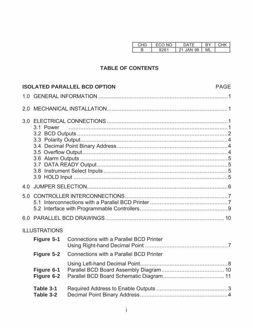
TABLE OF CONTENTS
ISOLATED PARALLEL BCD OPTION PAGE
1.0 GENERAL INFORMATION ..............................................................................1
2.0 MECHANICAL INSTALLATION.........................................................................1
3.0 ELECTRICAL CONNECTIONS .........................................................................13.1 Power ................................................................................................13.2 BCD Outputs ...........................................................................................23.3 Polarity Output.........................................................................................43.4 Decimal Point Binary Address...................................................................43.5 Overflow Output........................................................................................43.6 Alarm Outputs .........................................................................................53.7 DATA READY Output...............................................................................53.8 Instrument Select Inputs ...........................................................................53.9 HOLD Input .............................................................................................5
4.0 JUMPER SELECTION.....................................................................................6
5.0 CONTROLLER INTERCONNECTIONS..............................................................75.1 Interconnections with a Parallel BCD Printer ...............................................75.2 Interface with Programmable Controllers.....................................................9
6.0 PARALLEL BCD DRAWINGS........................................................................ 10
ILLUSTRATIONS
Figure 5-1 Connections with a Parallel BCD Printer Using Right-hand Decimal Point ..................................................7
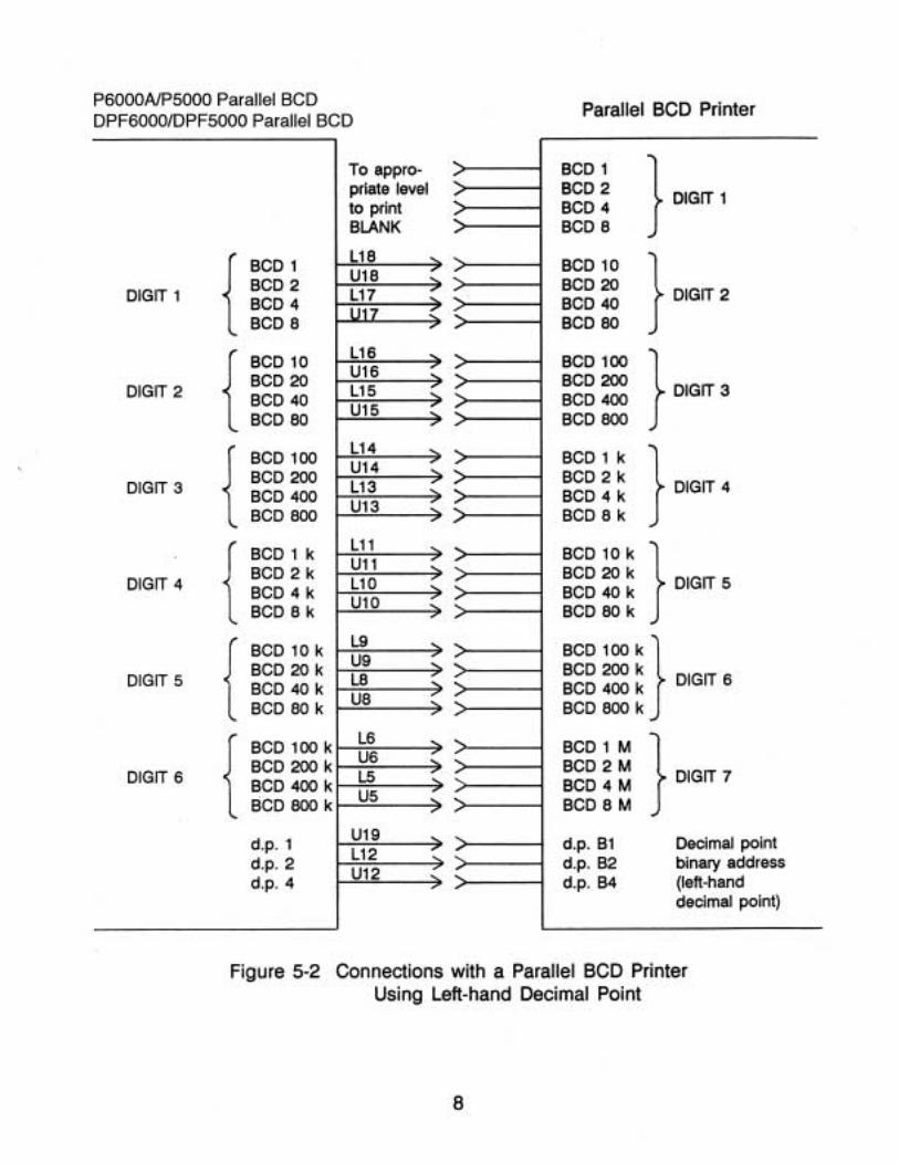
Figure 5-2 Connections with a Parallel BCD Printer
Using Left-hand Decimal Point.....................................................8Figure 6-1 Parallel BCD Board Assembly Diagram...................................... 10Figure 6-2 Parallel BCD Board Schematic Diagram..................................... 11
Table 3-1 Required Address to Enable Outputs ...........................................3Table 3-2 Decimal Point Binary Address.....................................................4
CHG ECO NO DATE BY CHKB 9261 21 JAN 98 ML
i i
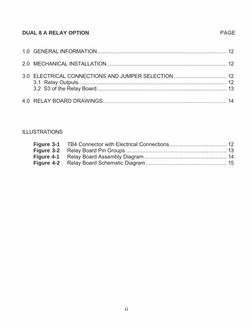
DUAL 8 A RELAY OPTION PAGE
1.0 GENERAL INFORMATION .............................................................................. 12
2.0 MECHANICAL INSTALLATION......................................................................... 12
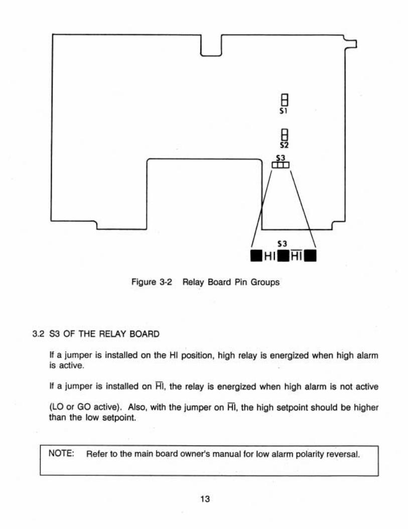
3.0 ELECTRICAL CONNECTIONS AND JUMPER SELECTION ................................ 123.1 Relay Outputs.......................................................................................... 123.2 S3 of the Relay Board............................................................................... 13
4.0 RELAY BOARD DRAWINGS........................................................................... 14
ILLUSTRATIONS
Figure 3-1 TB4 Connector with Electrical Connections................................... 12Figure 3-2 Relay Board Pin Groups ............................................................. 13Figure 4-1 Relay Board Assembly Diagram .................................................. 14Figure 4-2 Relay Board Schematic Diagram ................................................. 15
i i i
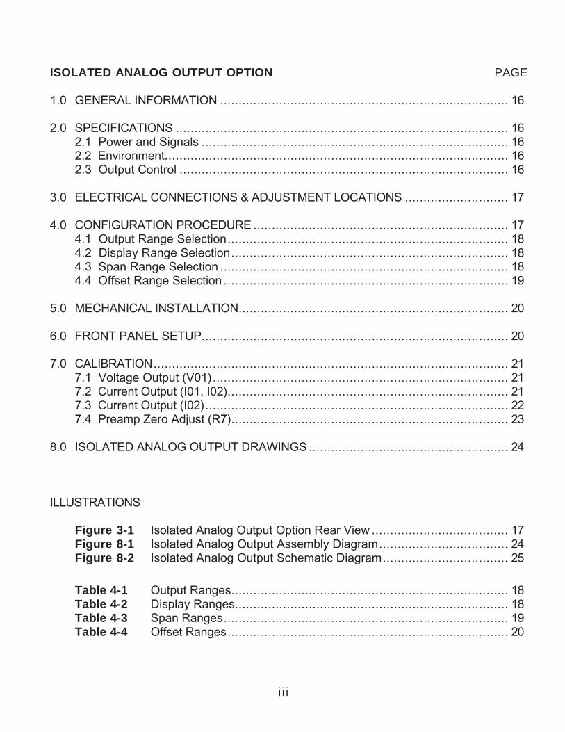
ISOLATED ANALOG OUTPUT OPTION PAGE
1.0 GENERAL INFORMATION .............................................................................. 16
2.0 SPECIFICATIONS .......................................................................................... 162.1 Power and Signals ................................................................................... 162.2 Environment............................................................................................. 162.3 Output Control ......................................................................................... 16
3.0 ELECTRICAL CONNECTIONS & ADJUSTMENT LOCATIONS ............................ 17
4.0 CONFIGURATION PROCEDURE ..................................................................... 174.1 Output Range Selection............................................................................ 184.2 Display Range Selection........................................................................... 184.3 Span Range Selection .............................................................................. 184.4 Offset Range Selection ............................................................................. 19
5.0 MECHANICAL INSTALLATION......................................................................... 20
6.0 FRONT PANEL SETUP................................................................................... 20
7.0 CALIBRATION................................................................................................ 217.1 Voltage Output (V01)................................................................................ 217.2 Current Output (I01, I02)............................................................................ 217.3 Current Output (I02).................................................................................. 227.4 Preamp Zero Adjust (R7)........................................................................... 23
8.0 ISOLATED ANALOG OUTPUT DRAWINGS ...................................................... 24
ILLUSTRATIONS
Figure 3-1 Isolated Analog Output Option Rear View ..................................... 17Figure 8-1 Isolated Analog Output Assembly Diagram................................... 24Figure 8-2 Isolated Analog Output Schematic Diagram.................................. 25
Table 4-1 Output Ranges........................................................................... 18Table 4-2 Display Ranges.......................................................................... 18Table 4-3 Span Ranges............................................................................. 19Table 4-4 Offset Ranges............................................................................ 20

2
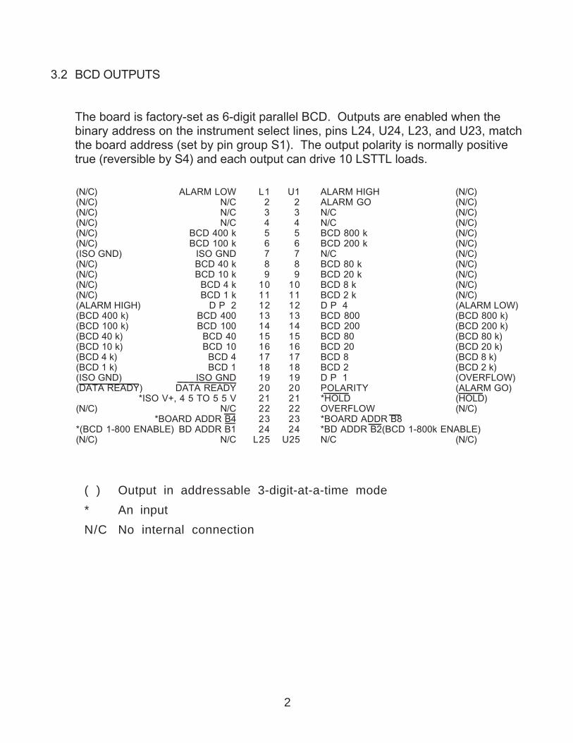
3.2 BCD OUTPUTS
The board is factory-set as 6-digit parallel BCD. Outputs are enabled when thebinary address on the instrument select lines, pins L24, U24, L23, and U23, matchthe board address (set by pin group S1). The output polarity is normally positivetrue (reversible by S4) and each output can drive 10 LSTTL loads.
(N/C) ALARM LOW L1 U1 ALARM HIGH (N/C)(N/C) N/C 2 2 ALARM GO (N/C)(N/C) N/C 3 3 N/C (N/C)(N/C) N/C 4 4 N/C (N/C)(N/C) BCD 400 k 5 5 BCD 800 k (N/C)(N/C) BCD 100 k 6 6 BCD 200 k (N/C)(ISO GND) ISO GND 7 7 N/C (N/C)(N/C) BCD 40 k 8 8 BCD 80 k (N/C)(N/C) BCD 10 k 9 9 BCD 20 k (N/C)(N/C) BCD 4 k 10 10 BCD 8 k (N/C)(N/C) BCD 1 k 11 11 BCD 2 k (N/C)(ALARM HIGH) D P 2 12 12 D P 4 (ALARM LOW)(BCD 400 k) BCD 400 13 13 BCD 800 (BCD 800 k)(BCD 100 k) BCD 100 14 14 BCD 200 (BCD 200 k)(BCD 40 k) BCD 40 15 15 BCD 80 (BCD 80 k)(BCD 10 k) BCD 10 16 16 BCD 20 (BCD 20 k)(BCD 4 k) BCD 4 17 17 BCD 8 (BCD 8 k)(BCD 1 k) BCD 1 18 18 BCD 2 (BCD 2 k)(ISO GND) ISO GND 19 19 D P 1 (OVERFLOW)(DATA READY) DATA READY 20 20 POLARITY (ALARM GO)
*ISO V+, 4 5 TO 5 5 V 21 21 *HOLD (HOLD) (N/C) N/C 22 22 OVERFLOW (N/C)
*BOARD ADDR B4 23 23 *BOARD ADDR B8*(BCD 1-800 ENABLE) BD ADDR B1 24 24 *BD ADDR B2(BCD 1-800k ENABLE)(N/C) N/C L25 U25 N/C (N/C)
( ) Output in addressable 3-digit-at-a-time mode
* An input
N/C No internal connection

3
To enable the outputs, install jumpers on the pin groups and apply the proper addresson the instrument select lines as indicated below:
6-DigitParallel BCD
S1 PositionsConnector P4 with
Instrument Select LinesU23 L23 U24 L24
Install jumpers on B8, B4, B2, B1* 0 0 0 0S2-A and S3-A; U5A B8, B4, B2, B1 0 0 0 1and U6A on XU5A B8, B4, B2, B1 0 0 1 0and XU6A sockets. B8, B4, B2, B1 0 0 1 1
B8, B4, B2, B1 0 1 0 0B8, B4, B2, B1 0 1 0 1B8, B4, B2, B1 0 1 1 0B8, B4, B2, B1 0 1 1 1
B8, B4, B2, B1 1 0 0 0B8, B4, B2, B1 1 0 0 1B8, B4, B2, B1 1 0 1 0B8, B4, B2, B1 1 0 1 1
B8, B4, B2, B1 1 1 0 0B8, B4, B2, B1 1 1 0 1B8, B4, B2, B1 1 1 1 0B8, B4, B2, B1 1 1 1 1
Addressable 3-DigitParallel BCD
S1 PositionsConnector P4 with
Instrument Select LinesU23 L23 U24 L24
ENABLES ENABLESBCD 1 - 800 BCD 1k - 800k
OVRFLW, HI,LO,GO D.P. 1,2,4, POLInstall a jumper onS2-B and S3-B. X, X, B2, B1 X, X, X, 0 X, X, 0, 1U5A and U6A on X, X, B2, B1 X, X, X, 1 X, X, 0, 0XU5B and XU6B X, X, B2, B1 X, X, X, 0 X, X, 1, 1sockets. X, X, B2, B1 X, X, X, 1 X, X, 1, 0
0 = Open or TTL High level (more than 2.0 V) X = Don't Care1 = Ground or TTL Low level (less than .8 V) * = Default Setting
Table 3-1 Required Address to Enable Outputs

4
3.3 POLARITY OUTPUT
This three-state output is active when Digits 1, 2 and 3 are enabled. Signalpolarity can be reversed by a push-on jumper at S4. With a jumper on S4-A, ahigh level corresponds to a positive display value.
3.4 DECIMAL POINT BINARY ADDRESS (D.P. 1, 2 AND 4)
These three-state outputs are enabled with Digits 1, 2 and 3. Signal polarity can bereversed by a push-on jumper at S4. With a jumper on S4-A, the outputs representpositive true binary address of a right-hand decimal point (see Table 3-2).
Decimal Point Position D.P. 4 D.P. 2 D.P. 1FFFFFF. 0 0 1FFFFF.F 0 1 0FFFF.FF 0 1 1FFF.FFF 1 0 0FF.FFFF 1 0 1F.FFFFF 1 1 0
Table 3-2 Decimal Point Binary Address
3.5 OVERFLOW OUTPUT
This three-state output is active when Digits 4, 5 and 6 are enabled. S4 reversesthe polarity. When a jumper is installed on S4-A, an overflow condition makes thisoutput go high. In this case, all of the digits of the parallel BCD boardrepresent a "9" (BCD 1001). The decimal point address corresponds to thepoint selected as Fixed Range decimal point. S7 connects this output topin U22 of the P4 connector.
5
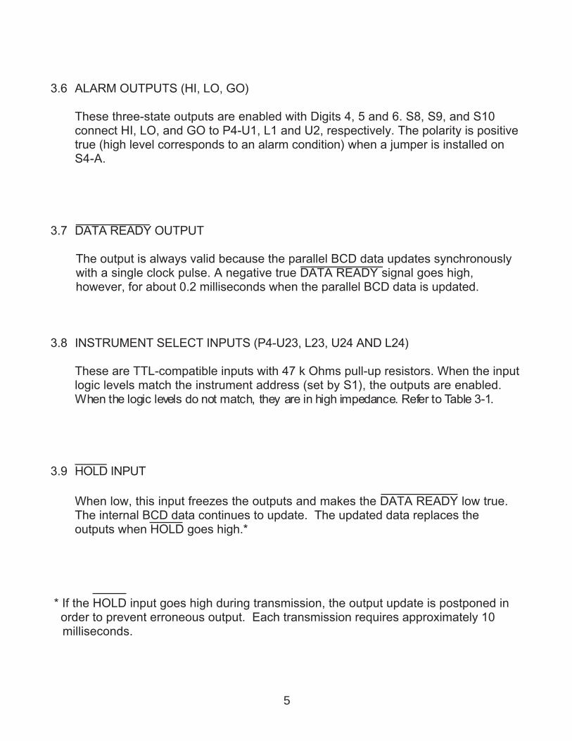
3.6 ALARM OUTPUTS (HI, LO, GO)
These three-state outputs are enabled with Digits 4, 5 and 6. S8, S9, and S10connect HI, LO, and GO to P4-U1, L1 and U2, respectively. The polarity is positivetrue (high level corresponds to an alarm condition) when a jumper is installed onS4-A.
3.7 DATA READY OUTPUT
The output is always valid because the parallel BCD data updates synchronouslywith a single clock pulse. A negative true DATA READY signal goes high,however, for about 0.2 milliseconds when the parallel BCD data is updated.
3.8 INSTRUMENT SELECT INPUTS (P4-U23, L23, U24 AND L24)
These are TTL-compatible inputs with 47 k Ohms pull-up resistors. When the inputlogic levels match the instrument address (set by S1), the outputs are enabled.When the logic levels do not match, they are in high impedance. Refer to Table 3-1.
3.9 HOLD INPUT
When low, this input freezes the outputs and makes the DATA READY low true.The internal BCD data continues to update. The updated data replaces theoutputs when HOLD goes high.*
* If the HOLD input goes high during transmission, the output update is postponed in order to prevent erroneous output. Each transmission requires approximately 10 milliseconds.
6
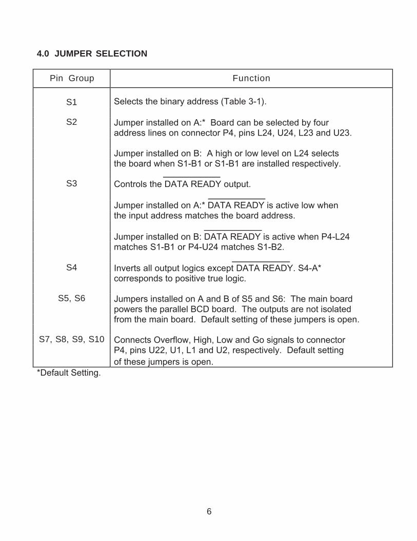
4.0 JUMPER SELECTION
Pin Group Function
S1 Selects the binary address (Table 3-1).
S2 Jumper installed on A:* Board can be selected by fouraddress lines on connector P4, pins L24, U24, L23 and U23.
Jumper installed on B: A high or low level on L24 selectsthe board when S1-B1 or S1-B1 are installed respectively.
S3 Controls the DATA READY output.
Jumper installed on A:* DATA READY is active low whenthe input address matches the board address.
Jumper installed on B: DATA READY is active when P4-L24matches S1-B1 or P4-U24 matches S1-B2.
S4 Inverts all output logics except DATA READY. S4-A*corresponds to positive true logic.
S5, S6 Jumpers installed on A and B of S5 and S6: The main boardpowers the parallel BCD board. The outputs are not isolatedfrom the main board. Default setting of these jumpers is open.
S7, S8, S9, S10 Connects Overflow, High, Low and Go signals to connectorP4, pins U22, U1, L1 and U2, respectively. Default settingof these jumpers is open.
*Default Setting.


9
5.2 INTERFACE WITH PROGRAMMABLE CONTROLLERS
If the controller can accept 24 bits of BCD data (32 bits if other data is alsorequired), the 6-digit parallel BCD mode can be used.
In addressable 3-digit-at-a-time mode, only half of the I/O lines are required. In thismode, digits 4, 5, and 6, Overflow, High, Low, and Go signals can be accessed onthe same lines of Digits 1, 2, and 3, D.P. 1, D.P.2, D.P. 4 and Polarity signals.Parallel BCD board can be configured as an addressable 3-digit-at-a-time BCD asfollows:
1. Move U5A and U5B integrated circuits (IC) to U5B and U6B sockets.
2. Install a jumper on S2-B and S3-B.
The outputs can be enabled by an appropriate logic level on U24 and L24 pins ofP4 (see Table 3-1).

10
6.0 PARALLEL BCD DRAWINGS
Figure 6-1 Parallel BCD Board Assembly Diagram

11

14
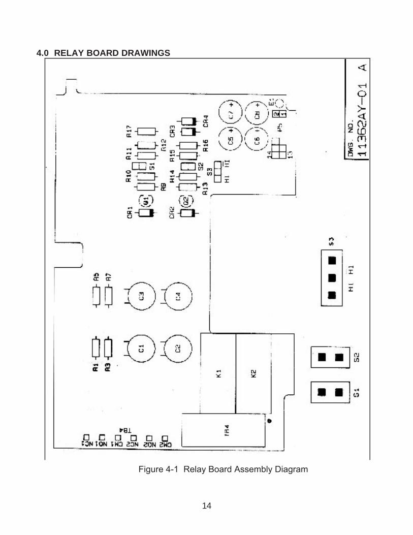
4.0 RELAY BOARD DRAWINGS
Figure 4-1 Relay Board Assembly Diagram

15

16
ISOLATED ANALOG OUTPUT OPTION1.0 GENERAL INFORMATION
The isolated analog output option provides 0 to 10 V, 0 to 20 mA or 4 to 20mA jumper-sellectable output ranges with 500 V isolation from the analogground of the main meter assembly.
Zero and span are each set with push-on jumpers on the circuit board forcoarse ranges plus a fine adjustment pot, which is accessible from the backof the meter. The coarse-span ranges are such that a span as narrow as500 counts or as wide as 9999 counts (the right four digits) can produce themaximum 10 V or 20 mA analog output. A NEGATIVE READING ISTREATED AS A ZERO READING.
The unit is further jumper-programmable to read either the left four digits (fordisplays such as 198800) or the right four digits (for displays such as001988).
2.0 SPECIFICATIONS
2.1 Power and Signals Supplied by basic meter via internal boardconnector (150 mA maximum)
2.2 Environment Same as the basic meter2.3 Output Control
Analog Voltage Range 0 to 10 V @ 20 mAAnalog Current Ranges 0 to 20 mA, 4 to 20 mA sourcing with 12 V
complianceOffset Ranges 4 coarse ranges of 0 to 25%, 25 to 50%, 50 to
75%, 75 to 100% with fine adjustment potaccessible from back of meter
Span Ranges 12 coarse ranges for 500 to 9999 counts (whenthe right four digits are selected) to produce themaximum 10 V or 20 mA output with fineadjustment pot accessible from back of meter
Turndown Ratio 20:1Zero Tempco 325 nA or 100µ V/°CSpan Tempco 0.0075% / ¡CLoad Regulation ±0.1%Full-scale Step Response 50 ms or less, 10 to 90%Resolution 0.05% of the output spanAccuracy (10 to 40¡C) ±0.1%Isolation 500 V from analog output to meter ground
17
NOTE: Unless otherwise specified, the unit is shipped in the default conditionwith 0 - 1M = 0 - 10 V or 1 mV/100 counts.
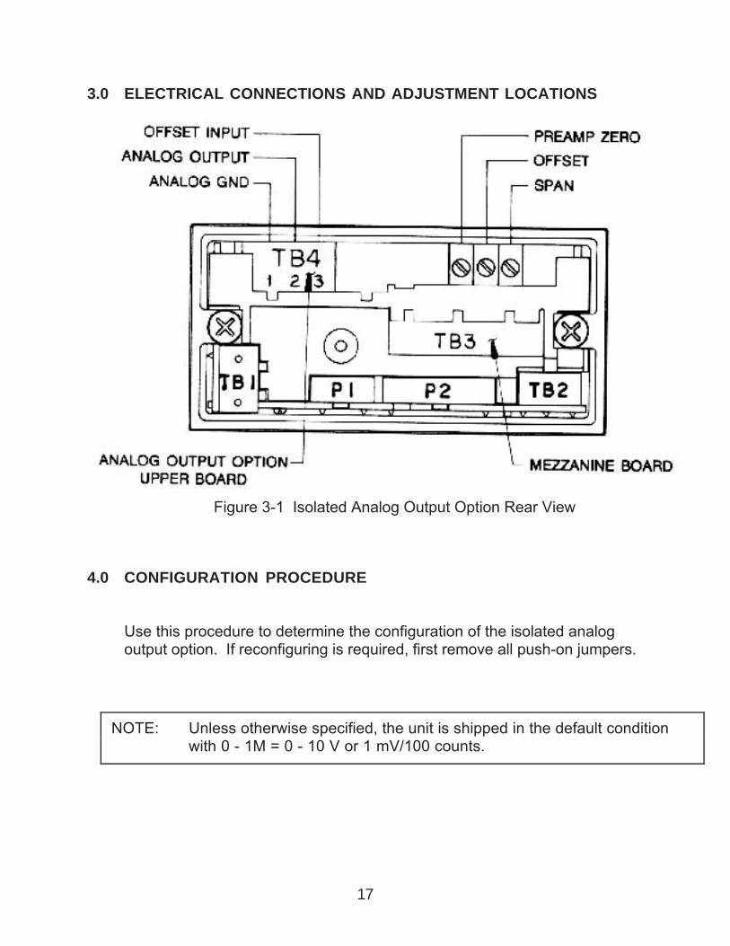
3.0 ELECTRICAL CONNECTIONS AND ADJUSTMENT LOCATIONS
Figure 3-1 Isolated Analog Output Option Rear View
4.0 CONFIGURATION PROCEDURE
Use this procedure to determine the configuration of the isolated analogoutput option. If reconfiguring is required, first remove all push-on jumpers.
18
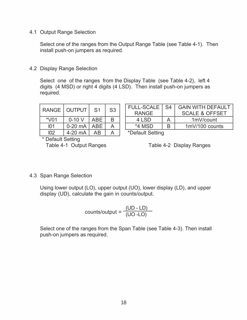
4.1 Output Range Selection
Select one of the ranges from the Output Range Table (see Table 4-1). Theninstall push-on jumpers as required.
4.2 Display Range Selection
Select one of the ranges from the Display Table (see Table 4-2), left 4digits (4 MSD) or right 4 digits (4 LSD). Then install push-on jumpers asrequired.
RANGE OUTPUT S1 S3 FULL-SCALERANGE
S4 GAIN WITH DEFAULTSCALE & OFFSET
*V01 0-10 V ABE B 4 LSD A 1mV/countI01 0-20 mA ABE A *4 MSD B 1mV/100 countsI02 4-20 mA AB A *Default Setting
* Default Setting Table 4-1 Output Ranges Table 4-2 Display Ranges
4.3 Span Range Selection
Using lower output (LO), upper output (UO), lower display (LD), and upperdisplay (UD), calculate the gain in counts/output.
(UD - LD)counts/output = (UO -LO)
Select one of the ranges from the Span Table (see Table 4-3). Then installpush-on jumpers as required.
19
NOTE: S1-E must be in, except on I02 range.
NOTE: When using the default (S4-B selecting the 4 MSD), divide displaycounts by 100 before using Table 4-3.
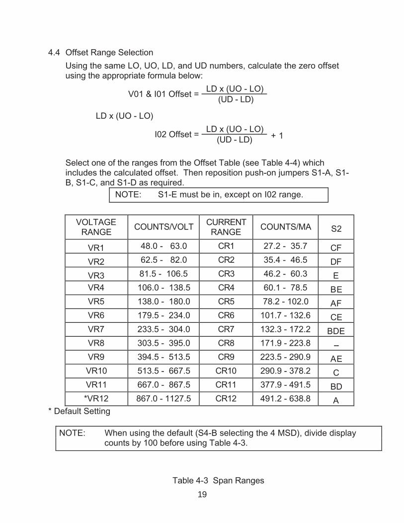
4.4 Offset Range Selection
Using the same LO, UO, LD, and UD numbers, calculate the zero offsetusing the appropriate formula below:
LD x (UO - LO)V01 & I01 Offset =
(UD - LD)
LD x (UO - LO)
LD x (UO - LO)I02 Offset =
(UD - LD) + 1
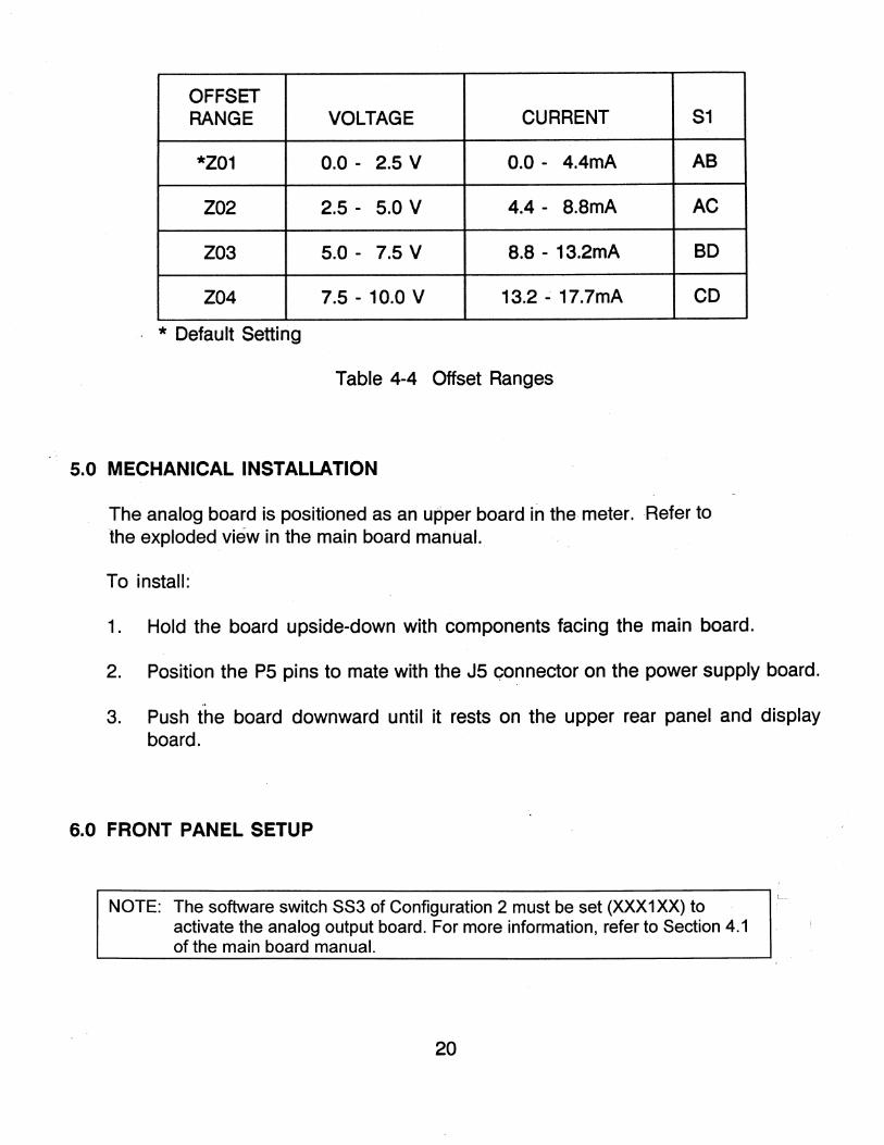
Select one of the ranges from the Offset Table (see Table 4-4) whichincludes the calculated offset. Then reposition push-on jumpers S1-A, S1-B, S1-C, and S1-D as required.
VOLTAGERANGE
COUNTS/VOLT CURRENTRANGE
COUNTS/MA S2
VR1 48.0 - 63.0 CR1 27.2 - 35.7 CF
VR2 62.5 - 82.0 CR2 35.4 - 46.5 DF
VR3 81.5 - 106.5 CR3 46.2 - 60.3 EVR4 106.0 - 138.5 CR4 60.1 - 78.5 BEVR5 138.0 - 180.0 CR5 78.2 - 102.0 AFVR6 179.5 - 234.0 CR6 101.7 - 132.6 CEVR7 233.5 - 304.0 CR7 132.3 - 172.2 BDEVR8 303.5 - 395.0 CR8 171.9 - 223.8 --VR9 394.5 - 513.5 CR9 223.5 - 290.9 AEVR10 513.5 - 667.5 CR10 290.9 - 378.2 CVR11 667.0 - 867.5 CR11 377.9 - 491.5 BD*VR12 867.0 - 1127.5 CR12 491.2 - 638.8 A
* Default Setting
Table 4-3 Span Ranges
21
7.0 CALIBRATION
Be sure to use the four display digits during calibration as selected inSection 4.2 .
NOTE: Calibration is possible without an input signal by setting FUNCTION toTOTAL and then OFFSET to the appropriate display reading.
7.1 Voltage output (V01)
1. Attach a voltmeter (4 1/2 digit or more) with the negative lead to TB4-1 and thepositive lead to TB4-2 on the rear panel of the unit.
2. Set the voltmeter range to 10 V dc full scale.
3. Apply a signal to the input which displays the lower display reading (LD) andadjust R8 (Z) to read the lower output voltage (LO) on the voltmeter.
4. Apply a signal to the input which displays the upper display reading (UD) andadjust R7 (S) to read the upper output voltage (UO) on the voltmeter.
5. Repeat steps 3 and 4 above.
7.2 Current Output (I01)
1. Attach an ammeter (4 1/2 digit or more) with the negative lead to TB4-1 andthe positive lead to TB4-2 on the rear panel of the unit.
2. Set the ammeter range to 20 mA full scale.
3. Apply a signal to the input which displays the lower display reading (LD) andadjust R8 (Z) to read the lower output current (LO) on the ammeter.
4. Apply a signal to the input which displays the upper display reading (UD) andadjust R7 (S) to read the upper output current (UO) on the ammeter.
5. Repeat steps 3 and 4 above.
22
7.3 Current Output (I02)
1. Attach an ammeter (4 1/2 digit or more) with the negative lead to TB4-1 andthe positive lead to TB4-2 on the rear panel of the unit.
2. Connect a jumper wire between TB4-1 and TB4-3.
3. Set the ammeter range to 20 mA full scale.
4. Apply a signal to the input which displays zero.
5. Record the ammeter reading (5.0 mA is typical).
6. Apply a signal to the input which is equal to the display span (UD - LD) andadjust R7 (S) on the ammeter to read the output span (UO - LO) plus theoffset recorded in step 5 (16.0 + 5.0 = 21.0 mA is typical).
7. Remove the jumper between TB4-1 and TB4-3.
8. Apply a signal to the input which displays the lower display reading (LD) andadjust R8 (Z) to read the lower output current (LO) on the ammeter.
9. Apply a signal to the input which displays the upper display reading (UD) andadjust R7 (S) to read the upper output current (UO) on the ammeter.
10. Repeat steps 8 and 9 above.
23
7.4 Preamp Zero Adjust (R9)
The preamp zero has been adjusted at the factory and should not requireadjustment unless it has been adjusted by mistake. If necessary, use thefollowing adjustment procedures:
1. For output ranges V01 and I01, apply a signal to the input which displays zeroon the selected display range (4 LSD OR 4 MSD). Jumper TB4-1 to TB4-3and adjust R9 for zero output on the voltmeter or ammeter. Proceed toSection 7.1 or 7.2 .
2. For output range I02, you must add S1-E push-on jumper before performingstep 1 above. After completing step 1, you must remove S1-E beforeproceeding to Section 7.3.
24
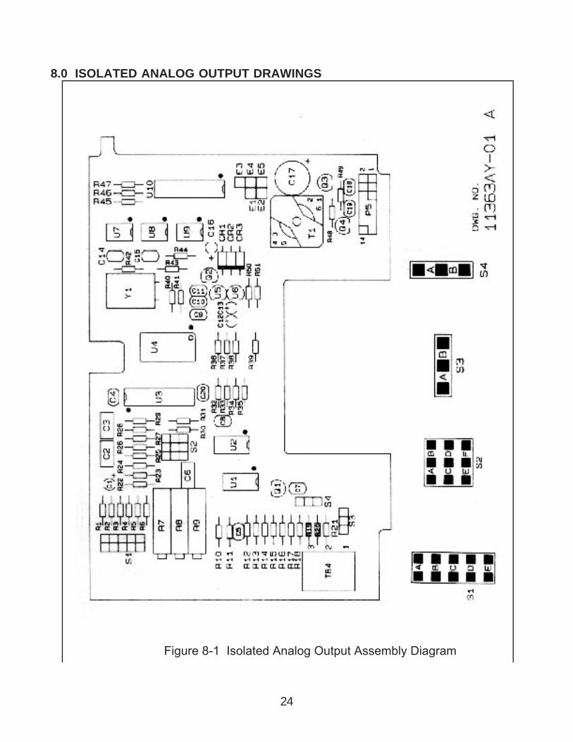
8.0 ISOLATED ANALOG OUTPUT DRAWINGS
Figure 8-1 Isolated Analog Output Assembly Diagram
25
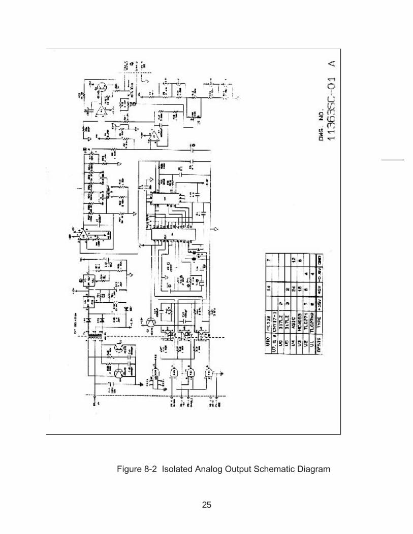
Figure 8-2 Isolated Analog Output Schematic Diagram

Warranty/DisclaimerNEWPORT Electronics, Inc. warrants this unit to be free of defects in materials and workmanship for a period of one(1) year from the date of purchase. In addition to NEWPORT’s standard warranty period, NEWPORT Electronics willextend the warranty period for one (1) additional year if the warranty card enclosed with each instrument is returnedto NEWPORT.
If the unit should malfunction, it must be returned to the factory for evaluation. NEWPORT’s Customer ServiceDepartment will issue an Authorized Return (AR) number immediately upon phone or written request. Uponexamination by NEWPORT, if the unit is found to be defective it will be repaired or replaced at no charge.NEWPORT’s WARRANTY does not apply to defects resulting from any action of the purchaser, including but notlimited to mishandling, improper interfacing, operation outside of design limits, improper repair, or unauthorizedmodification. This WARRANTY is VOID if the unit shows evidence of having been tampered with or shows evidenceof being damaged as a result of excessive corrosion; or current, heat, moisture or vibration; improper specification;misapplication; misuse or other operating conditions outside of NEWPORT’s control. Components which wear are notwarranted, including but not limited to contact points, fuses, and triacs.
NEWPORT is pleased to offer suggestions on the use of its various products. However, NEWPORT neitherassumes responsibility for any omissions or errors nor assumes liability for any damages that result from theuse of its products in accordance with information provided by NEWPORT, either verbal or written. NEWPORTwarrants only that the parts manufactured by it will be as specified and free of defects. NEWPORT MAKES NOOTHER WARRANTIES OR REPRESENTATIONS OF ANY KIND WHATSOEVER, EXPRESSED OR IMPLIED,EXCEPT THAT OF TITLE, AND ALL IMPLIED WARRANTIES INCLUDING ANY WARRANTY OFMERCHANTABILITY AND FITNESS FOR A PARTICULAR PURPOSE ARE HEREBY DISCLAIMED. LIMITATIONOF LIABILITY: The remedies of purchaser set forth herein are exclusive and the total liability of NEWPORTwith respect to this order, whether based on contract, warranty, negligence, indemnification, strict liability orotherwise, shall not exceed the purchase price of the component upon which liability is based. In no eventshall NEWPORT be liable for consequential, incidental or special damages.
CONDITIONS: Equipment sold by NEWPORT is not intended to be used, nor shall it be used: (1) as a “BasicComponent” under 10 CFR 21 (NRC), used in or with any nuclear installation or activity; or (2) in medical applicationsor used on humans. Should any Product(s) be used in or with any nuclear installation or activity, medical application,or used on humans, or misused in any way, NEWPORT assumes no responsibility as set forth in our basicWARRANTY / DISCLAIMER language, and additionally purchaser will indemnify NEWPORT and hold NEWPORTharmless from any liability or damage whatsoever arising out of the use of the Product(s) in such a manner.
Direct all warranty and repair requests/inquiries to the NEWPORT Customer ServiceDepartment. BEFORE RETURNING ANY PRODUCT(S) TO NEWPORT, PURCHASER MUSTOBTAIN AN AUTHORIZED RETURN (AR) NUMBER FROM NEWPORT’S CUSTOMERSERVICE DEPARTMENT (IN ORDER TO AVOID PROCESSING DELAYS). The assigned ARnumber should then be marked on the outside of the return package and on anycorrespondence.The purchaser is responsible for shipping charges, freight, insurance and proper packaging toprevent breakage in transit.
FOR WARRANTY RETURNS, pleasehave the following information availableBEFORE contacting NEWPORT:1. P.O. number under which the product
was PURCHASED,2. Model and serial number of the product
under warranty, and3. Repair instructions and/or specific
problems relative to the product.
FOR NON-WARRANTY REPAIRS, consultNEWPORT for current repair charges. Have thefollowing information available BEFOREcontacting NEWPORT:1. P.O. number to cover the COST of
the repair,2. Model and serial number of product, and3. Repair instructions and/or specific problems
relative to the product.
NEWPORT’s policy is to make running changes, not model changes, whenever an improvement is possible. Thisaffords our customers the latest in technology and engineering.NEWPORT is a registered trademark of NEWPORT Electronics, Inc.© Copyright 2003 NEWPORT Electronics, Inc. All rights reserved. This document may not be copied,photocopied, reproduced, translated, or reduced to any electronic medium or machine-readable form, in whole or inpart, without prior written consent of NEWPORT Electronics, Inc.
Return Requests/Inquiries

M913/N/0103 11361ML-01 Rev. D
For immediate technical or application assistance please call:
Newport Electronics, Inc.2229 South Yale Street • Santa Ana, CA • 92704 • U.S.A.
TEL: (714) 540-4914 • FAX: (203) 968-7311Toll Free: 1-800-639-7678 • www.newportUS.com • e-mail:[email protected]
ISO 9001 Certified
Newport Technologies, Inc.976 Bergar • Laval (Quebec) • H7L 5A1 • Canada
TEL: (514) 335-3183 • FAX: (514) 856-6886Toll Free: 1-800-639-7678 • www.newport.ca • e-mail:[email protected]
Newport Electronics, Ltd.One Omega Drive • River Bend Technology Centre
Northbank, Irlam • Manchester M44 5BD • United KingdomTel: +44 161 777 6611 • FAX: +44 161 777 6622
Toll Free: 0800 488 488 • www.newportuk.co.uk • e-mail:[email protected]
Newport Electronics B.V.Postbus 8034 • 1180 LA Amstelveen • The Netherlands
TEL: +31 20 3472121 • FAX: +31 20 6434643Toll Free: 0800 0993344 • www.newport.nl • e-mail: [email protected]
Newport Electronics spol s.r.o.Frystatska 184, 733 01 Karviná • Czech RepublicTEL: +420 59 6311899 • FAX: +420 59 6311114
Toll Free: 0800-1-66342 • www.newport.cz • e-mail: [email protected]
Newport Electronics GmbHDaimlerstrasse 26 • D-75392 Deckenpfronn • Germany
TEL: 49 7056 9398-0 • FAX: 49 7056 9398-29Toll Free: 0800 / 6397678 • www.newport.de • e-mail: [email protected]
Newport Electronique S.A.R.L.11, rue Jacques Cartier • 78280 Guyancourt • France
TEL: +33 1 61 37 29 00 • FAX: +33 1 30 57 54 27Toll Free: 0800 466 342 • www.newport.fr • e-mail: [email protected]
Mexico and Latin AmericaFAX: 001 (203) 359-7807
En Español: 001 (203) 359-7803
®