GEETHANJALI COLLEGE OF ENGINEERING AND...
60
1 GEETHANJALI COLLEGE OF ENGINEERING AND TECHNOLOGY Cheeryal (V), Keesara (M), R. R. District ELECTRONIC CIRCUITS LAB STUDENTS’ MANUAL …striving toward perfection DEPARTMENT OF ELECTRONICS AND COMMUNICATION ENGINEERING Lab Incharge: HOD-ECE: J. Mrudula Dr.P.Srihari Associate Professor
Transcript of GEETHANJALI COLLEGE OF ENGINEERING AND...

1
GEETHANJALI COLLEGE OF ENGINEERING AND
TECHNOLOGY
Cheeryal (V), Keesara (M), R. R. District
ELECTRONIC CIRCUITS LAB
STUDENTS’ MANUAL
…striving toward perfection
DEPARTMENT OF
ELECTRONICS AND COMMUNICATION ENGINEERING
Lab Incharge: HOD-ECE:
J. Mrudula Dr.P.Srihari
Associate Professor
2
GEETHANJALI COLLEGE OF ENGINEERING & TECHNOLOGY
Cheeryal (V), Keesara (M), R. R. District
…striving toward perfection
LABORATORY MANUAL
FOR
ELECTRONIC CIRCUITS LAB
Prepared by: Checked by:
Ms. J. Mrudula Prof. K. Somasekhara Rao,
Assoc.Prof Dean of Academics, Dept., of ECE
Approved by:
Dr.P.Srihari,HOD
Dept., of ECE
3
GEETHANJALI COLLEGE OF ENGINEERING AND TECHNOLOGY
DEPARTMENT OF Electronics and Communications Engineering
(Name of the Subject / Lab Course) : Electronic circuits Lab
(JNTU CODE -) A40484 Programme : UG
Branch: ECE Version No : 01
Year: II Updated on : 02/12/2015
Semester: II No. of pages :
Classification status (Unrestricted / Restricted ): Unrestricted
Distribution List :Department , Lab, Library, Lab incharge
Prepared by : 1) Name : J. Mrudula 1) Name :
2) Sign : 2) Sign :
3) Design : Associate professor 3) Design :
4) Date : 02/12/2015 4) Date : 02/12/2015
Verified by : 1) Name :Prof. K. Somasekhara Rao
2) Sign :
3) Design : Professor
4) Date :
* For Q.C Only.
1) Name :
2) Sign :
3) Design :
4) Date :
Approved by : (HOD ) 1) Name : Dr.P.Srihari
2) Sign :
3) Date :
4
ECE DEPARTMENT
Vision of the Department
To impart quality technical education in Electronics and Communication Engineering
emphasizing analysis, design/synthesis and evaluation of hardware/embedded software using
various Electronic Design Automation (EDA) tools with accent on creativity, innovation and
research thereby producing competent engineers who can meet global challenges with societal
commitment.
Mission of the Department
i. To impart quality education in fundamentals of basic sciences, mathematics, electronics and
communication engineering through innovative teaching-learning processes.
ii. To facilitate Graduates define, design, and solve engineering problems in the field of
Electronics and Communication Engineering using various Electronic Design Automation
(EDA) tools.
iii. To encourage research culture among faculty and students thereby facilitating them to be
creative and innovative through constant interaction with R & D organizations and Industry.
iv. To inculcate teamwork, imbibe leadership qualities, professional ethics and social
responsibilities in students and faculty.
Program Educational Objectives of B. Tech (ECE) Program:
I. To prepare students with excellent comprehension of basic sciences, mathematics and
engineering subjects facilitating them to gain employment or pursue postgraduate studies
with an appreciation for lifelong learning.
II. To train students with problem solving capabilities such as analysis and design with
adequate practical skills wherein they demonstrate creativity and innovation that would
enable them to develop state of the art equipment and technologies of multidisciplinary
nature for societal development.
III. To inculcate positive attitude, professional ethics, effective communication and
interpersonal skills which would facilitate them to succeed in the chosen profession
exhibiting creativity and innovation through research and development both as team
member and as well as leader.
5
Program Outcomes of B.Tech ECE Program:
1. An ability to apply knowledge of Mathematics, Science, and Engineering to solve complex
engineering problems of Electronics and Communication Engineering systems.
2. An ability to model, simulate and design Electronics and Communication Engineering
systems, conduct experiments, as well as analyze and interpret data and prepare a report
with conclusions.
3. An ability to design an Electronics and Communication Engineering system, component,
or process to meet desired needs within the realistic constraints such as economic,
environmental, social, political, ethical, health and safety, manufacturability and
sustainability.
4. An ability to function on multidisciplinary teams involving interpersonal skills.
5. An ability to identify, formulate and solve engineering problems of multidisciplinary
nature.
6. An understanding of professional and ethical responsibilities involved in the practice of
Electronics and Communication Engineering profession.
7. An ability to communicate effectively with a range of audience on complex engineering
problems of multidisciplinary nature both in oral and written form.
8. The broad education necessary to understand the impact of engineering solutions in a
global, economic, environmental and societal context.
9. A recognition of the need for, and an ability to engage in life-long learning and acquire the
capability for the same.
10. A knowledge of contemporary issues involved in the practice of Electronics and
Communication Engineering profession
11. An ability to use the techniques, skills and modern engineering tools necessary for
engineering practice.
12. An ability to use modern Electronic Design Automation (EDA) tools, software and
electronic equipment to analyze, synthesize and evaluate Electronics and Communication
Engineering systems for multidisciplinary tasks.
13. Apply engineering and project management principles to one's own work and also to
manage projects of multidisciplinary nature.
6
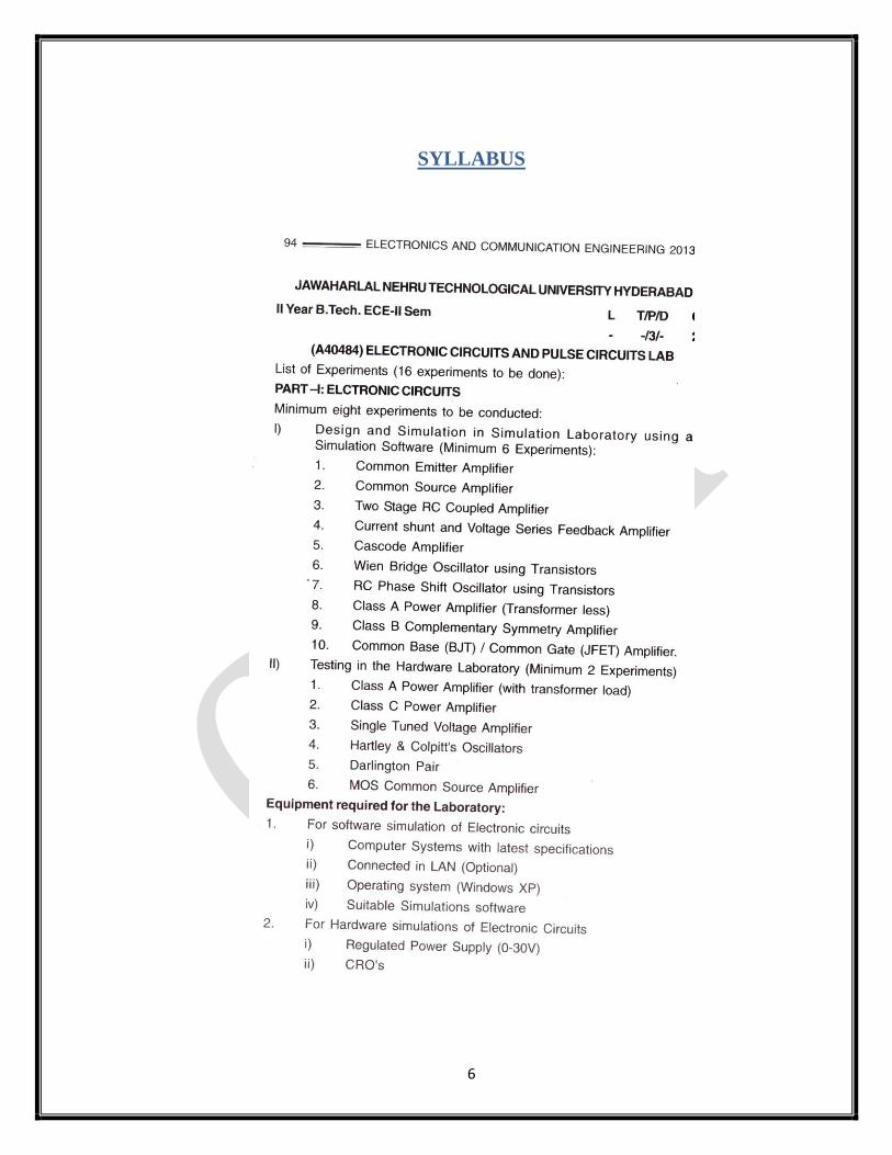
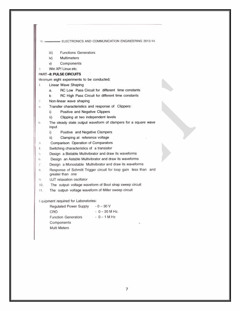
SYLLABUS
7

8
INSTRUCTIONS
Instruction for students:-
1. Do not handle any equipment without reading the instructions /Instruction manuals.
2. Observe type of sockets of equipment power to avoid mechanical damage.
3. Do not insert connectors forcefully in the sockets.
4. Strictly observe the instructions given by the Teacher/ Lab Instructor.
5. After the experiment is over, the students must hand over the Bread board, Trainer kits, wires,
CRO probes and other components to the lab assistant/teacher.
6. It is mandatory to come to lab in a formal dress (Shirts, Trousers, ID card, and Shoes for boys).
Strictly no Jeans for both Girls and Boys.
7. It is mandatory to come with observation book and lab record in which previous experiment should
be written in Record and the present lab’s experiment in Observation book.
8. Observation book of the present lab experiment should be get corrected on the same day and
Record should be corrected on the next scheduled lab session.
9. Mobile Phones should be Switched OFF in the lab session.
10. Students have to come to lab in-time. Late comers are not allowed to enter the lab.
11. Prepare for the viva questions. At the end of the experiment, the lab faculty will ask the viva
questions and marks are allotted accordingly.
12. Bring all the required stationery like graph sheets, pencil & eraser, different color pens etc. for the
lab class.
13. While shorting 2 or more wires for common connections like grounding, do not twist wires. Use
shorting link on the bread board.
Instructions to Laboratory Teachers:-
1. Observation book and lab records submitted for the lab work are to be checked and signed before
the next lab session.
2. Students should be instructed to switch ON the power supply after the connections are checked by
the lab assistant / teacher.
3. The promptness of submission of records/ observation books should be strictly insisted by awarding
the marks accordingly.
4. Ask viva questions at the end of the experiment.
5. Do not allow students who come late to the lab class.
6. Encourage the students to do the experiments innovatively.
9
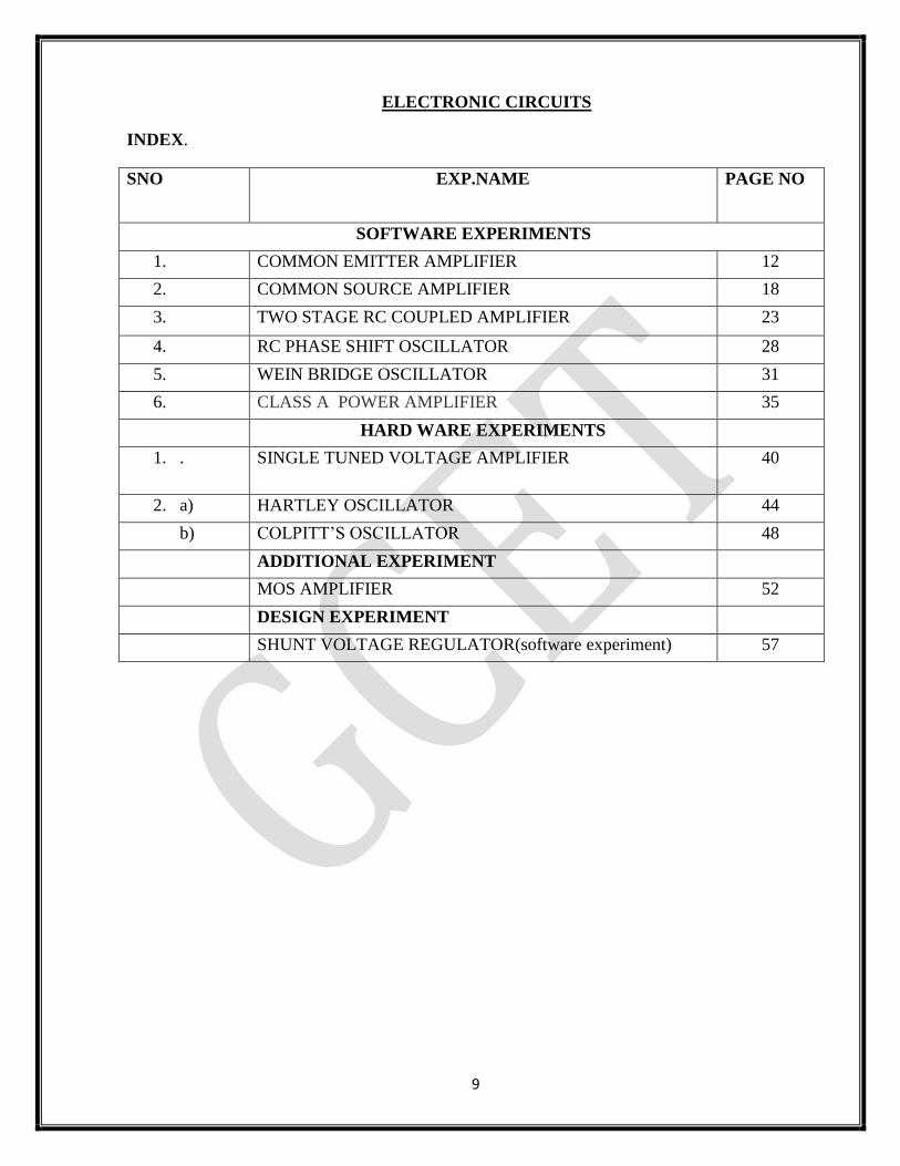
ELECTRONIC CIRCUITS
INDEX.
SNO EXP.NAME PAGE NO
SOFTWARE EXPERIMENTS
1. COMMON EMITTER AMPLIFIER 12
2. COMMON SOURCE AMPLIFIER 18
3. TWO STAGE RC COUPLED AMPLIFIER 23
4. RC PHASE SHIFT OSCILLATOR 28
5. WEIN BRIDGE OSCILLATOR 31
6. CLASS A POWER AMPLIFIER 35
HARD WARE EXPERIMENTS
1. . SINGLE TUNED VOLTAGE AMPLIFIER 40
2. a) HARTLEY OSCILLATOR 44
b) COLPITT’S OSCILLATOR 48
ADDITIONAL EXPERIMENT
MOS AMPLIFIER 52
DESIGN EXPERIMENT
SHUNT VOLTAGE REGULATOR(software experiment) 57
10
ELECTRONIC CIRCUITS
11
Exp 1. TRANSISTOR CE AMPLIFIER
OBJECTIVE: 1. To Design Transistor CE amplifier and simulating in MULTISIM software
and find its voltage gain.
2. To draw the frequency response curve of CE amplifier.
APPARATUS:
MULTISIM 2001 SOFTWARE
PC
THEORY:
The CE amplifier provides high gain and wide frequency response. The emitter lead is
common to both input and output circuits and is grounded. The emitter-base circuit is forward
biased. The collector current is controlled by the base current rather than emitter current. The
input signal is applied to base terminal of the transistor and amplifier output is taken across
collector terminal. A very small change in base current produces a much larger change in collector
current. When +ve half-cycle is fed to the input circuit, it opposes the forward bias of the circuit
which causes the collector current to decrease, it decreases the voltage more –ve. When input
cycle varies through a -ve half-cycle, it increases the forward bias of the circuit, which causes the
collector current to increases thus the output signal in common emitter amplifier is in out of
phase with the input signal.
CIRCUIT DIAGRAM:

12
PROCEDURE:
1. Start MULTISIM. A blank circuit window will appear on the screen along with a component
tool bar.
2. Using component tool bar, place all the components on the circuit window and wire the
circuit.
3. Connect the circuit as shown in circuit diagram
4. Apply the input of 50mV peak-to-peak and 1 KHz frequency sinusoidal, using AC Voltage
Source
5. Measure the Output Voltage Vo (p-p) for different frequencies
6. Tabulate the readings in the tabular form.
7. The voltage gain can be calculated by using the expression
Av= (V0/Vi)
8. For plotting the frequency response the input voltage is kept constant at 50mV peak-to-peak
and the frequency is varied from 10Hz to 1MHz using function generator
9. Note down the value of output voltage for each frequency.
10. All the readings are tabulated and voltage gain in dB is calculated by usingThe expression
` Av=20 log10 (V0/Vi)
13
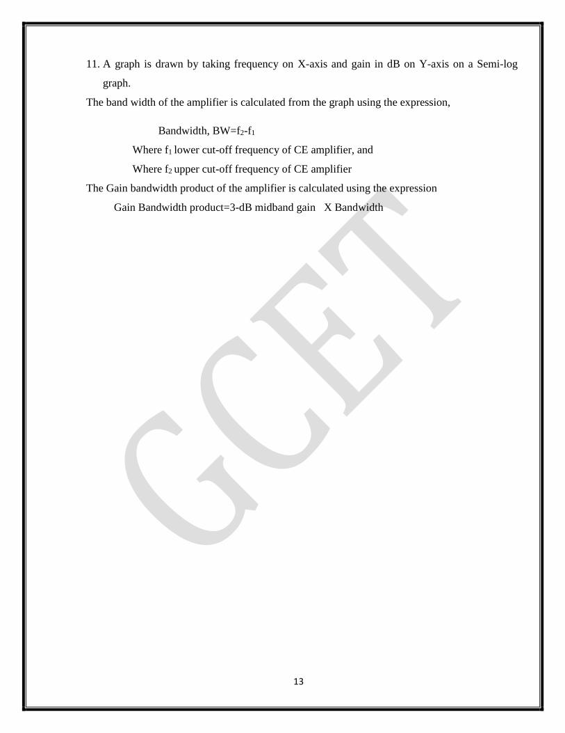
11. A graph is drawn by taking frequency on X-axis and gain in dB on Y-axis on a Semi-log
graph.
The band width of the amplifier is calculated from the graph using the expression,
Bandwidth, BW=f2-f1
Where f1 lower cut-off frequency of CE amplifier, and
Where f2 upper cut-off frequency of CE amplifier
The Gain bandwidth product of the amplifier is calculated using the expression
Gain Bandwidth product=3-dB midband gain X Bandwidth

14
OBSERVATIONS:
Input voltage Vin =50mV
FREQUENCY(Hz) OUTPUT
VOLTAGE (Vo)
Gain = Vo/Vin GAIN IN dB
Av=20log10
(V0/Vin)
10
50
100
200
400
600
800
1K
5K
10K
50K
100K
200K
400K
600K
800K
1M
MODELWAVE FORMS:

15
INPUT WAVE FORM:
OUTPUT WAVE FORM

16
FREQUENCY RESPONSE:
RESULT: The voltage gain and frequency response of the CE amplifier are obtained. Also
gain bandwidth product of the amplifier is calculated.
LEARNING OUTCOMES:
Students are able to
1. Design and analyze CE amplifier using MULTISIM software.
2. Calculate voltage gain and bandwidth of CE amplifier from the observations made.
Mid band
frequency
range
17
VIVA QUESTIONS:
1. What is phase difference between input and output waveforms of CE amplifier?
2. What type of biasing is used in the above given circuit?
3. If the given transistor is replaced by a p-n-p, can we amplify the signals and explain?
4. What is effect of emitter-bypass capacitor on frequency response?
5. What is the effect of coupling capacitor?
6. What is the region of the transistor so that it can be operated as an amplifier?
7. How does transistor acts as an amplifier?
8. Draw the h-parameter model of CE amplifier?
9. What type of transistor configuration is used in intermediate stages of a multistage amplifier?
10. What is Early effect?

18
Exp.2. COMMON SOURCE FET AMPLIFIER
OBJECTIVE: 1. To obtain the frequency response of the Common Source FET Amplifier
2. To find the Bandwidth.
APPRATUS:
MULTISIM 2001 SOFTWARE
PC
CIRCUIT DIAGRAM:
THEORY:
A field-effect transistor (FET) is a type of transistor commonly used for weak-signal
amplification (for example, for amplifying wireless (signals)). The device can amplify analog or
digital signals. It can also switch DC or function as an oscillator. In the FET, current flows along
a semiconductor path called the channel. At one end of the channel, there is an electrode called
the source. At the other end of the channel, there is an electrode called the drain. The physical
diameter of the channel is fixed, but its effective electrical diameter can be varied by the
application of a voltage to a control electrode called the gate. Field-effect transistors exist in two
major classifications. These are known as the junction FET (JFET) and the metal-oxide-
19
semiconductor FET (MOSFET). The junction FET has a channel consisting of N-type
semiconductor (N-channel) or P-type semiconductor (P-channel) material; the gate is made of
the opposite semiconductor type. In P-type material, electric charges are carried mainly in the
form of electron deficiencies called holes. In N-type material, the charge carriers are primarily
electrons. In a JFET, the junction is the boundary between the channel and the gate. Normally,
this P-N junction is reverse-biased (a DC voltage is applied to it) so that no current flows
between the channel and the gate. However, under some conditions there is a small current
through the junction during part of the input signal cycle. The FET has some advantages and
some disadvantages relative to the bipolar transistor. Field-effect transistors are preferred for
weak-signal work, for example in wireless, communications and broadcast receivers. They are
also preferred in circuits and systems requiring high impedance. The FET is not, in general, used
for high-power amplification, such as is required in large wireless communications and
broadcast transmitters.
Field-effect transistors are fabricated onto silicon integrated circuit (IC) chips. A single IC
can contain many thousands of FETs, along with other components such as resistors, capacitors,
and diodes.
PROCEDURE:
1. Start MULTISIM. A blank circuit window will appear on the screen along with a
component tool bar.
2. Using component tool bar place all the components on the circuit window and wire the
circuit.
3. A sinusoidal signal of 1 KHz frequency and 200mV peak-to-peak is applied at the input of
amplifier.
4. Output is taken at drain and gain is calculated by using the expression,
Av=V0/Vi
5. Voltage gain in dB is calculated by using the expression,
Av=20log 10(V0/Vi)
6. Repeat the above steps for different frequencies.
7. For plotting the frequency response the input voltage is kept Constant at 50mV peak-to-
peak and the frequency is varied from 10Hz to 1MHz using AC Voltage Source.
8. The Bandwidth of the amplifier is calculated from the graph using the
9. Expression,
Bandwidth BW=f2-f1
Where f1 is lower 3 dB frequency
f2 is upper 3 dB frequency
20
OBSERVATIONS:
Input Voltage given Vin:50mV
Frequency(Hz) Output
Voltage
(Vo)
Gain= Vo/Vin
Av in dB
20 log (Vo/Vin)
10
50
100
200
400
600
800
1K
5K
10K
50K
100K
200K
400K
600K
800K
1M
MODEL GRAPH:
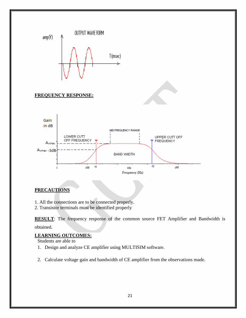
21
FREQUENCY RESPONSE:
PRECAUTIONS
1. All the connections are to be connected properly.
2. Transistor terminals must be identified properly
RESULT: The frequency response of the common source FET Amplifier and Bandwidth is
obtained.
LEARNING OUTCOMES:
Students are able to
1. Design and analyze CE amplifier using MULTISIM software.
2. Calculate voltage gain and bandwidth of CE amplifier from the observations made.
22
VIVA QUESTIONS
1. What are the differences between FET and BJT?
2. Is FET an unipolar or bipolar device ?
3. Draw the symbol of FET?
4. What are the applications of FET?
5. Is FET a voltage controlled or current controlled device?
6. Draw the equivalent circuit of common source FET amplifier?
7. What is the voltage gain of the FET amplifier?
8. What is the input impedance of FET amplifier?
9. What is the output impedance of FET amplifier?
10. What are the FET parameters?
23
Exp.3. TWO STAGE RC COUPLED AMPLIFIER
OBJECTIVES: 1.To obtain the frequency response of the Two Stage RC Coupled Amplifier
2. To find the Voltage Gain and Bandwidth.
APPARATUS:
MULTISIM 2001 SOFTWARE
PC
THEORY:
This is most popular type of coupling as it provides excellent audio fidelity. A coupling
capacitor is used to connect output of first stage to input of second stage. Resistances R5, R2, R3
form biasing and stabilization network for Q1 and R7, R8 and R9 for Q2. Emitter bypass capacitor
offers low reactance paths to signal. coupling Capacitor transmits AC signal, blocks DC.
Cascaded stages amplify the signal, the overall gain is increased. Thus coupling is done for more
gain and overall gain of two stages equals to A=A1*A2
A1=voltage gain of first stage=V01/Vi
A2=voltage gain of second stage= V02/V01
A= V02/Vi
When ac signal is applied to the base of the transistor, its amplified output appears across the
collector resistor Rc. It is given to the second stage for further amplification and signal appears
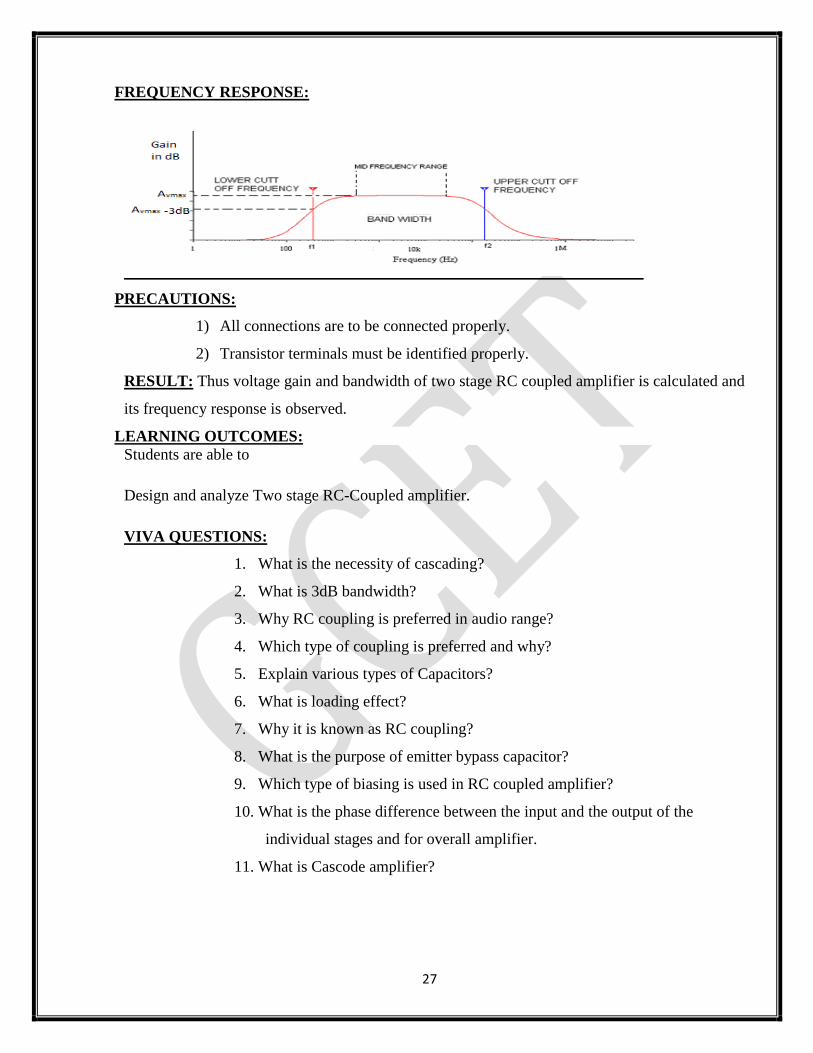
with more strength. Frequency response curve is obtained by plotting a graph between
frequency and gain in dB .The gain is constant in mid frequency range and gain decreases on
both sides of the mid frequency range. The gain decreases in the low frequency range due to
coupling capacitor Cc and at high frequencies due to junction capacitance Cbe.
24
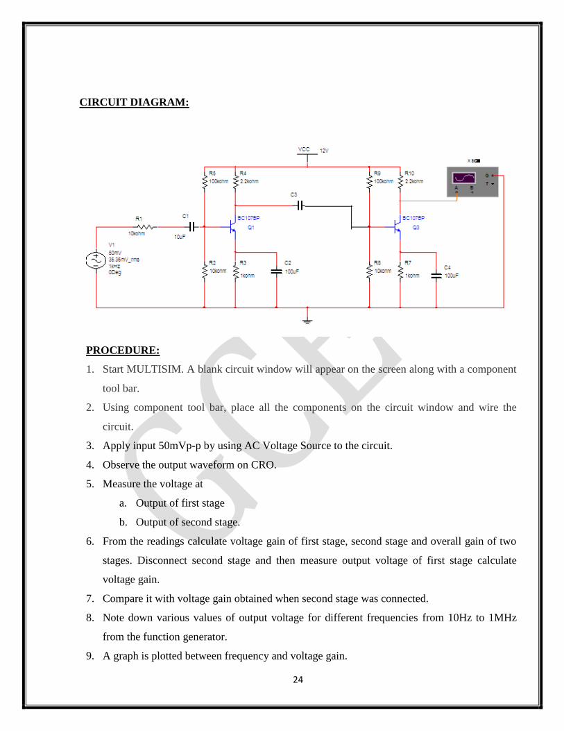
CIRCUIT DIAGRAM:
PROCEDURE:
1. Start MULTISIM. A blank circuit window will appear on the screen along with a component
tool bar.
2. Using component tool bar, place all the components on the circuit window and wire the
circuit.
3. Apply input 50mVp-p by using AC Voltage Source to the circuit.
4. Observe the output waveform on CRO.
5. Measure the voltage at
a. Output of first stage
b. Output of second stage.
6. From the readings calculate voltage gain of first stage, second stage and overall gain of two
stages. Disconnect second stage and then measure output voltage of first stage calculate
voltage gain.
7. Compare it with voltage gain obtained when second stage was connected.
8. Note down various values of output voltage for different frequencies from 10Hz to 1MHz
from the function generator.
9. A graph is plotted between frequency and voltage gain.
25
OBSERVATIONS: -
Vin = 50mVp-p
FREQUENCY(HZ)
O/P
VOLTAGE
(Vo)
Gain = Vo/Vin VOLTAGE GAIN
in dB (20 log10Vo/Vin)
10
50
100
200
400
600
800
1K
5K
10K
50K
100K
200K
400K
600K
800K
1M
26
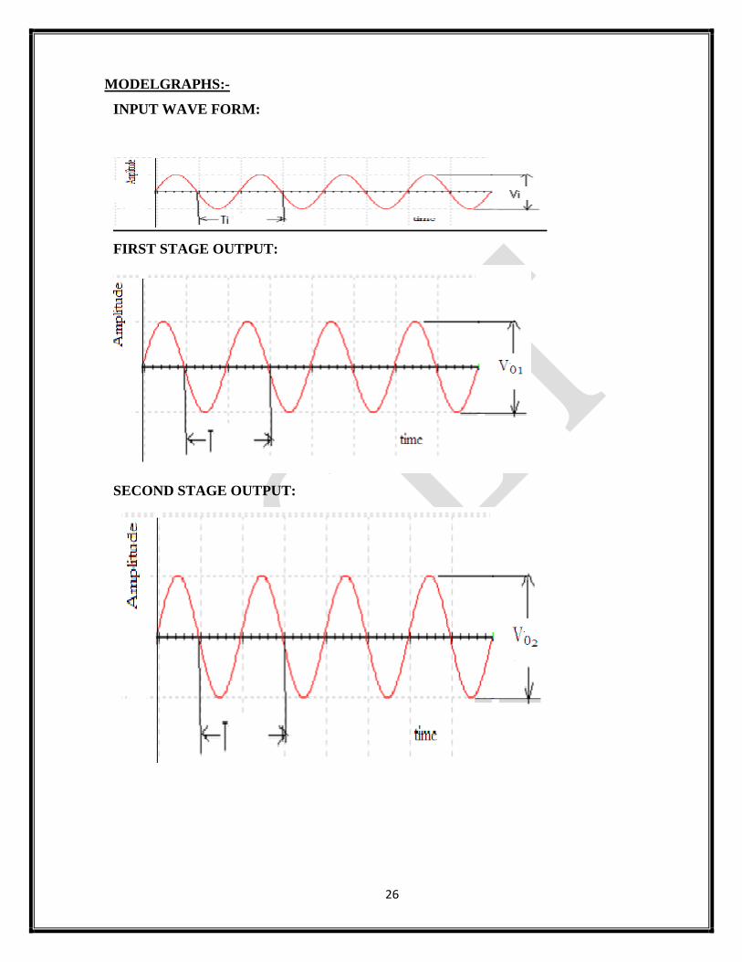
MODELGRAPHS:-
INPUT WAVE FORM:
FIRST STAGE OUTPUT:
SECOND STAGE OUTPUT:
27
FREQUENCY RESPONSE:
PRECAUTIONS:
1) All connections are to be connected properly.
2) Transistor terminals must be identified properly.
RESULT: Thus voltage gain and bandwidth of two stage RC coupled amplifier is calculated and
its frequency response is observed.
LEARNING OUTCOMES:
Students are able to
Design and analyze Two stage RC-Coupled amplifier.
VIVA QUESTIONS:
1. What is the necessity of cascading?
2. What is 3dB bandwidth?
3. Why RC coupling is preferred in audio range?
4. Which type of coupling is preferred and why?
5. Explain various types of Capacitors?
6. What is loading effect?
7. Why it is known as RC coupling?
8. What is the purpose of emitter bypass capacitor?
9. Which type of biasing is used in RC coupled amplifier?
10. What is the phase difference between the input and the output of the
individual stages and for overall amplifier.
11. What is Cascode amplifier?
28
Exp.4 RC PHASE SHIFT OSCILLATOR
OBJECTIVE:
To calculate the frequency of oscillations of RC phase shift oscillator & to compare
theoretical and practical value.
Objective:
APPARATUS:
MULTISIM 2001 SOFTWARE
PC
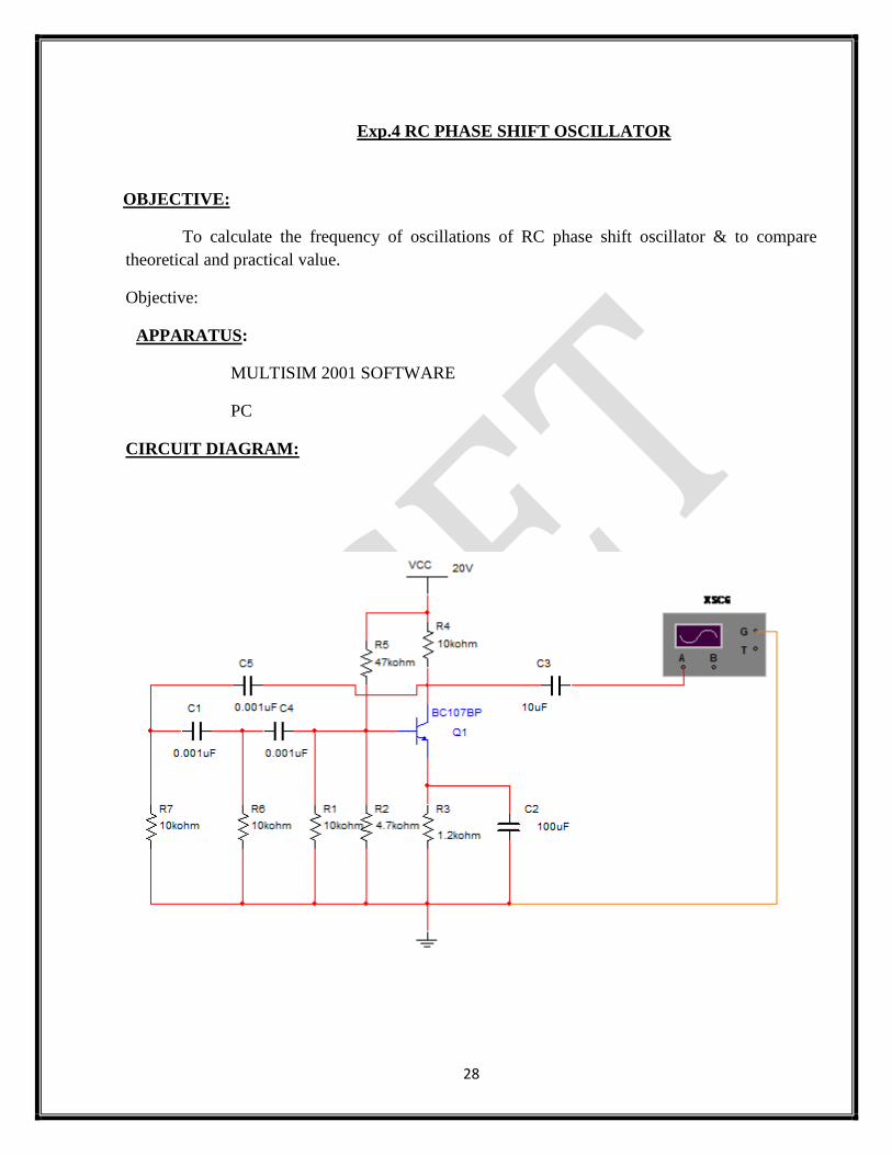
CIRCUIT DIAGRAM:
29
THEORY:
RC-Phase shift Oscillator has a CE amplifier followed by three sections of RC phase
shift feedback Networks. The output of the last stage is returned to the input of the amplifier.
The values of R and C are chosen such that the phase shift of each RC section is 60º.Thus The
RC ladder network produces a total phase shift of 180º between its input and output voltage for
the given frequencies. Since CE Amplifier produces 180 º phase shift, the total phase shift from
the base of the transistor around the circuit and back to the base will be exactly 360º or 0º. This
satisfies the Barkhausen condition for sustaining oscillations.Total loop gain of this circuit is
greater than or equal to 1, this condition used to generate the sinusoidal oscillations.
The frequency of oscillations of RC-Phase Shift Oscillator is,
f = 1/2πRC√6
PROCEDURE:
1. Start MULTISIM. A blank circuit window will appear on the screen along with a component
tool bar.
2. Using component tool bar place all the components on the circuit window and wire the
circuit.
3. Observe the output signal and note down the output amplitude and time period (Td).
4. Calculate the frequency of oscillations theoretically and verify it practically (f=1/Td).
5. Repeat the above procedure for different values of R & C.
THEORITICAL CALCULATIONS: R = 10KΩ, C = 0.001 μf
f = 1/2πRC√(6+4k) where k = Rc/R
PRACTICAL CALCULATIONS:
Td = time period of oscillations
f = 1/Td
Tabular column:
Resistance(Ω) Theoretical frequency
(KHz)
Practical frequency
(KHz)
10k
1k
15k
22k
30
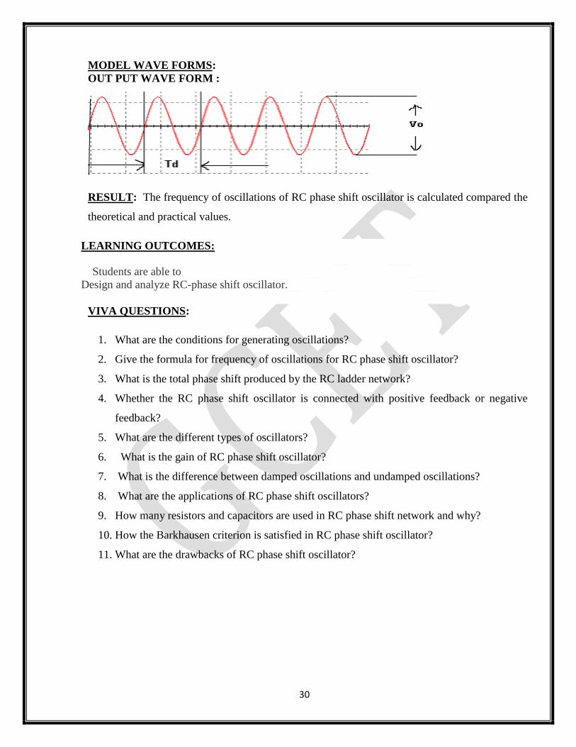
MODEL WAVE FORMS:
OUT PUT WAVE FORM :
RESULT: The frequency of oscillations of RC phase shift oscillator is calculated compared the
theoretical and practical values.
LEARNING OUTCOMES:
Students are able to
Design and analyze RC-phase shift oscillator.
VIVA QUESTIONS:
1. What are the conditions for generating oscillations?
2. Give the formula for frequency of oscillations for RC phase shift oscillator?
3. What is the total phase shift produced by the RC ladder network?
4. Whether the RC phase shift oscillator is connected with positive feedback or negative
feedback?
5. What are the different types of oscillators?
6. What is the gain of RC phase shift oscillator?
7. What is the difference between damped oscillations and undamped oscillations?
8. What are the applications of RC phase shift oscillators?
9. How many resistors and capacitors are used in RC phase shift network and why?
10. How the Barkhausen criterion is satisfied in RC phase shift oscillator?
11. What are the drawbacks of RC phase shift oscillator?

31
Exp.5 .WEIN BRIDGE OSCILLATOR
OBJECTIVE::
To study and calculate frequency of oscillations of Wein Bridge Oscillator and compare it
with theoretical value.
APPARATUS:
MULTISIM 2007 SOFTWARE
PC
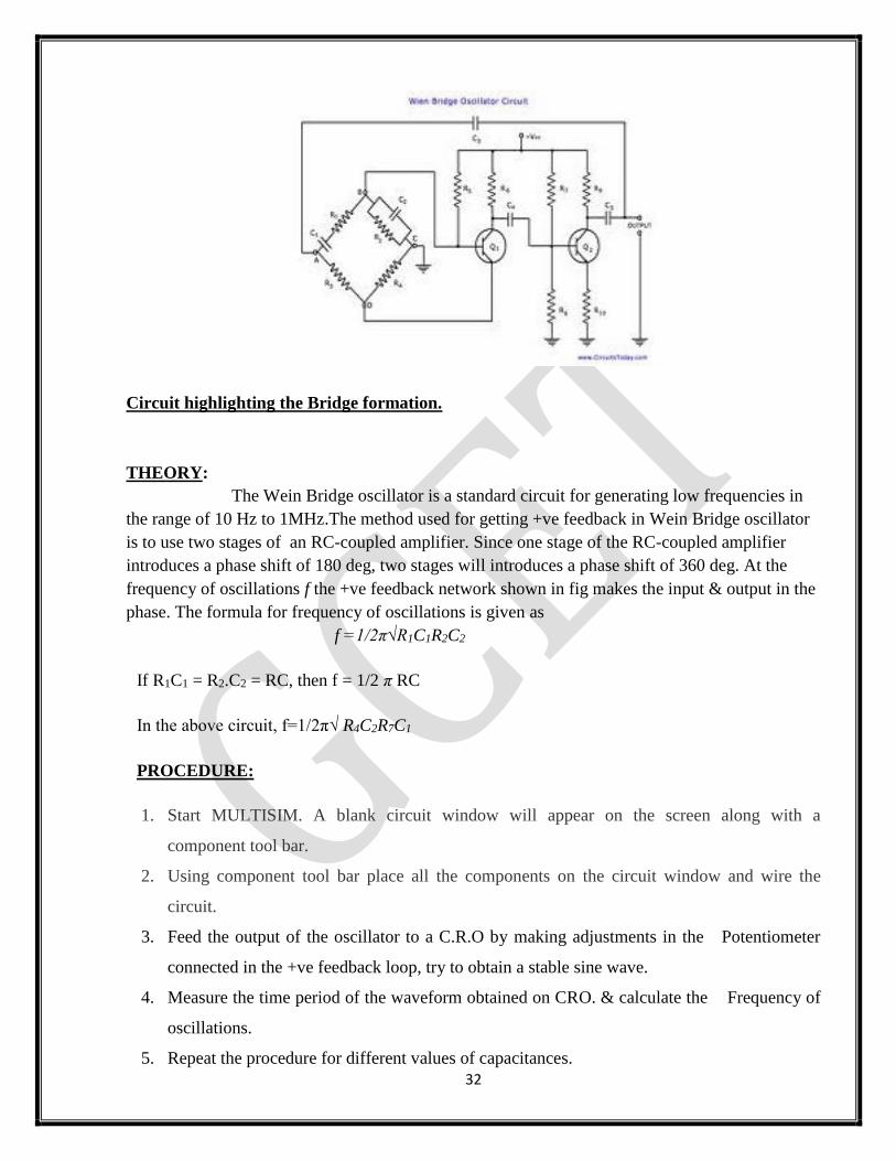
CIRCUITDIAGRAM:
32
Circuit highlighting the Bridge formation.
THEORY:
The Wein Bridge oscillator is a standard circuit for generating low frequencies in
the range of 10 Hz to 1MHz.The method used for getting +ve feedback in Wein Bridge oscillator
is to use two stages of an RC-coupled amplifier. Since one stage of the RC-coupled amplifier
introduces a phase shift of 180 deg, two stages will introduces a phase shift of 360 deg. At the
frequency of oscillations f the +ve feedback network shown in fig makes the input & output in the
phase. The formula for frequency of oscillations is given as
f =1/2π√R1C1R2C2
If R1C1 = R2.C2 = RC, then f = 1/2 π RC
In the above circuit, f=1/2π√ R4C2R7C1
PROCEDURE:
1. Start MULTISIM. A blank circuit window will appear on the screen along with a
component tool bar.
2. Using component tool bar place all the components on the circuit window and wire the
circuit.
3. Feed the output of the oscillator to a C.R.O by making adjustments in the Potentiometer
connected in the +ve feedback loop, try to obtain a stable sine wave.
4. Measure the time period of the waveform obtained on CRO. & calculate the Frequency of
oscillations.
5. Repeat the procedure for different values of capacitances.
33
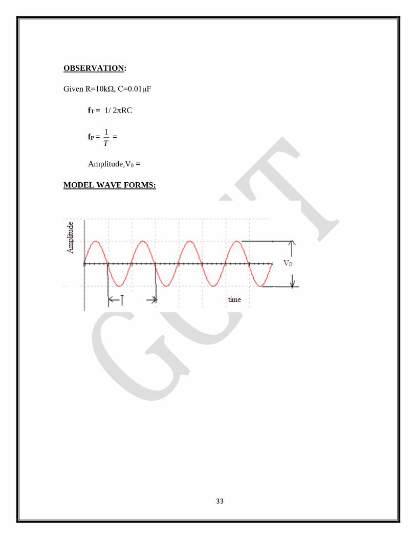
OBSERVATION:
Given R=10kΩ, C=0.01μF
fT = 1/ 2RC
fP = T
1 =
Amplitude,V0 =
MODEL WAVE FORMS:
34
RESULT:
The frequency of oscillations of the Wein Bridge oscillator is calculated and is verified.
LEARNING OUTCOMES:
Students are able to
Design and analyze Wein Bridge oscillator.
VIVA QUESTIONS:
1. Give the formula for frequency of oscillations in Wein Bridge Oscillator circuit?
2. What is the condition for Wien Bridge oscillator to generate oscillations?
3. What is the total phase shift provided by the Wein Bridge oscillator?
4. What is the function of lead-lag network in Wein Bridge oscillator?
5. Which type of feedback is used in Wein Bridge oscillator
6. What is the gain of Wein Bridge oscillator?
7. What are the applications of Wein Bridge oscillator
8. What is the condition for generating oscillations?
9. What is the difference between damped oscillations undamped oscillations?
10. Wein Bridge oscillator is either LC or RC oscillator.
11. What are the drawbacks in using Wein Bridge Oscillators?
35
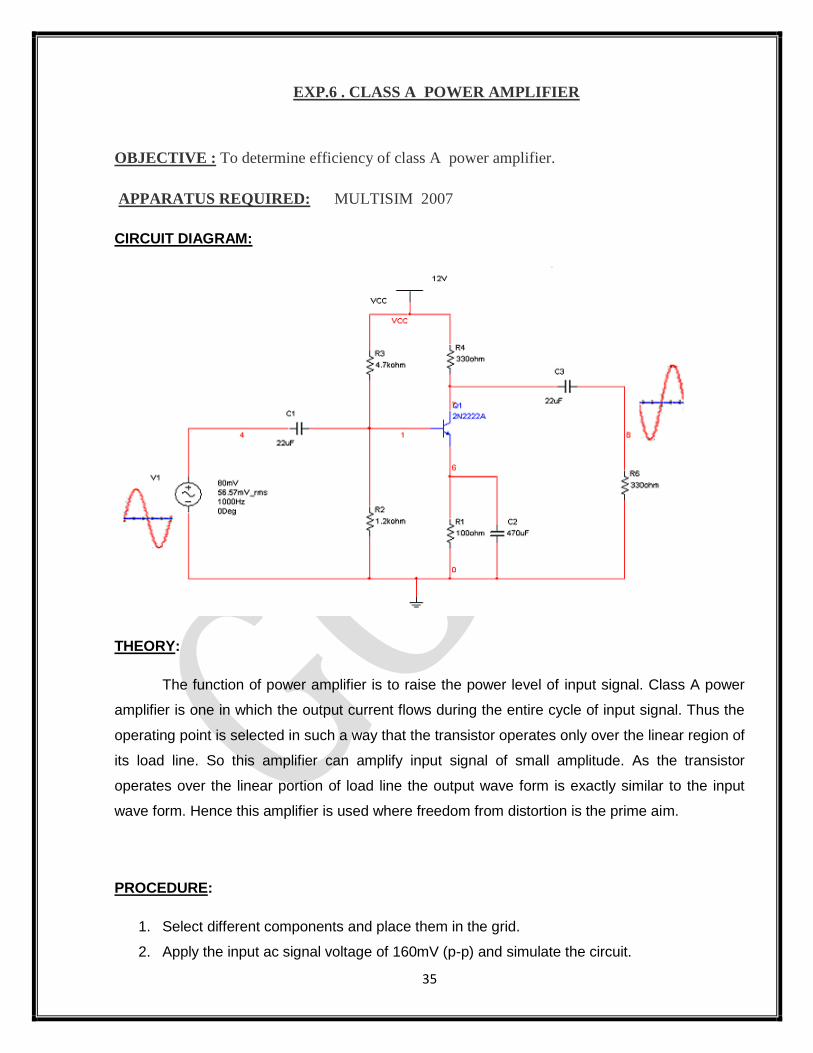
EXP.6 . CLASS A POWER AMPLIFIER
OBJECTIVE : To determine efficiency of class A power amplifier.
APPARATUS REQUIRED: MULTISIM 2007
CIRCUIT DIAGRAM:
THEORY:
The function of power amplifier is to raise the power level of input signal. Class A power
amplifier is one in which the output current flows during the entire cycle of input signal. Thus the
operating point is selected in such a way that the transistor operates only over the linear region of
its load line. So this amplifier can amplify input signal of small amplitude. As the transistor
operates over the linear portion of load line the output wave form is exactly similar to the input
wave form. Hence this amplifier is used where freedom from distortion is the prime aim.
PROCEDURE:
1. Select different components and place them in the grid.
2. Apply the input ac signal voltage of 160mV (p-p) and simulate the circuit.

36
3. Observe the output wave form on CRO and measure the output voltage V0.
4. Now connect the ammeter at collector terminal of transistor.
5. Disconnect the ac signal from input and measure the collector current Ic in ammeter.
6. calculate the efficiency by using practical calculations compare it with theoretically
calculated efficiency
OBSERVATION :
THEORITICAL CALCULATIONS :
ICQ =
ICQ =
Pin(dc) = =
Po(a.c) =
(Imax – Imin) =
(Vmax –Vmin) = VCC
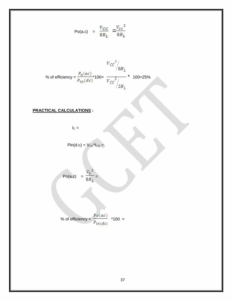
37
Po(a.c) = =
% of efficiency = *100= * 100=25%
PRACTICAL CALCULATIONS :
IC =
Pin(d.c) = VCC*ICQ =
Po(a.c) = =
% of efficiency = *100 =
38
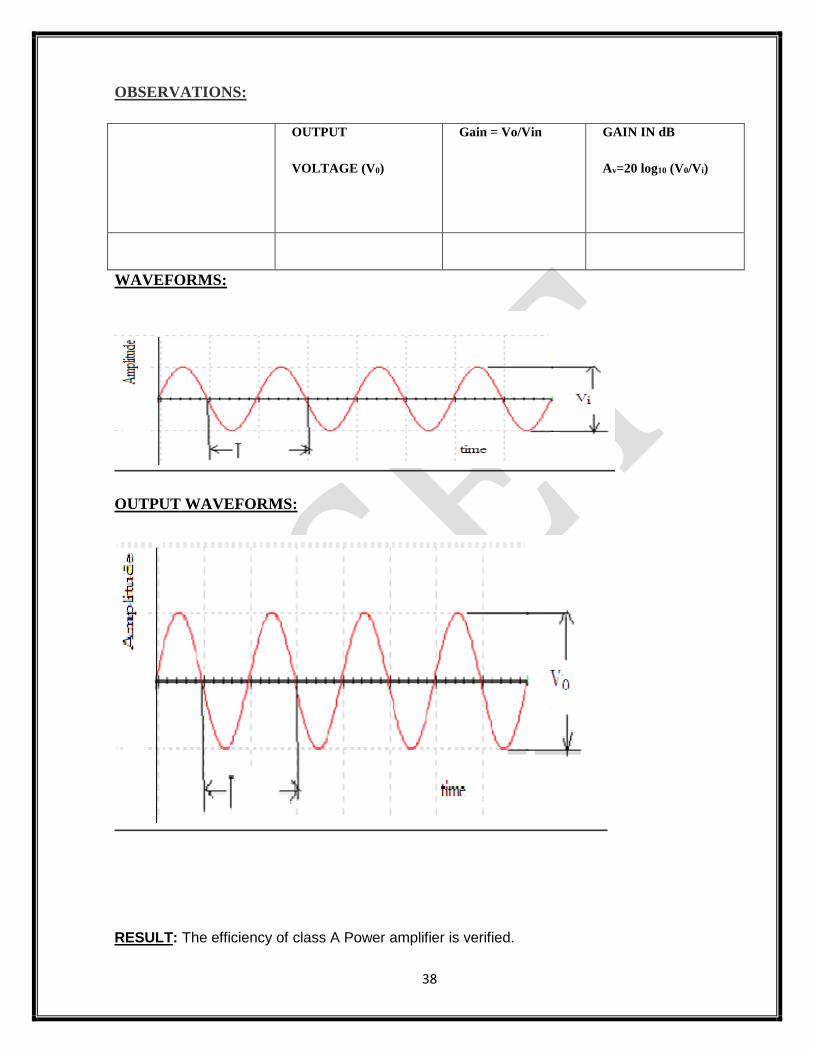
OBSERVATIONS:
OUTPUT
VOLTAGE (V0)
Gain = Vo/Vin GAIN IN dB
Av=20 log10 (V0/Vi)
WAVEFORMS:
OUTPUT WAVEFORMS:
RESULT: The efficiency of class A Power amplifier is verified.
39
LEARNING OUTCOMES:
Students are able to
Design and analyze class A power amplifier.
VIVA QUESTIONS:
1. Define class A power amplifier?
2. Give the reason why class A power amplifier is called as directly coupled power
amplifier?
3. What is the efficiency of class A power amplifier?
4. In a power transistor, when the maximum power dissipation takes place?
5. List out the different types of distortions?
6. Define Harmonic distortion?
7. What are Class B, Class C and Class AB amplifiers and which type is used for what
application?
40
HARDWARE EXPERIMENTS
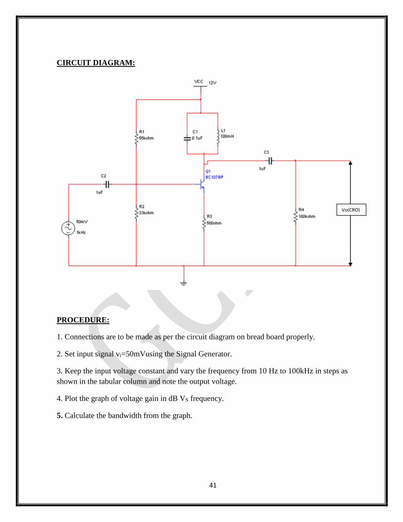
Exp 1. SINGLE TUNED VOLTAGE AMPLIFIER
OBJECTIVE: To plot the frequency response of a single tuned voltage amplifier.
APPARATUS :
Transistor BC107 - 1 No.
Resistors 33kΩ -1No.
56kΩ -1No.
100kΩ -1No.
560Ω -1No.
Capacitors 0.1µf -1No.
1µf 2 Nos.
Inductor 100 mH -1No.
CRO(Dual Channel) (0-20 MHz)
Function generator ( 1Hz to 1 MHz)
Regulated power supply (0-30V)
Breadboard
Connecting wires.
THEORY:
The signal to be amplified and it is applied between the terminals base and emitter. The
tank circuit (i.e L & R) is located at collector terminal and it may be varied in such a way that
the resonant frequency becomes equal to the frequency of the input signal. At resonant the tuned
circuit offers high impedance and thus given input signal is amplified and thus appears with large
value across it and other frequencies will be rejected. The response of the tuned amplifiers falls
sharply below and above the resonant frequency. So the tuned circuit selects the desired
frequency and rejects all other frequencies.
41
CIRCUIT DIAGRAM:
PROCEDURE:
1. Connections are to be made as per the circuit diagram on bread board properly.
2. Set input signal vi=50mVusing the Signal Generator.
3. Keep the input voltage constant and vary the frequency from 10 Hz to 100kHz in steps as
shown in the tabular column and note the output voltage.
4. Plot the graph of voltage gain in dB VS frequency.
5. Calculate the bandwidth from the graph.
Vo(CRO)

42
OBSERVATIONS:
Tabular form:
frequency Gain=(Vo/Vi) Gain in dB= 20log(gain)
10Hz
100Hz
500Hz
1kHz
1.2khz
1.22kHz
1.24kHz
1.26kHz
1.28kHz
1.30kHz
1.32kHz
1.34kHz
1.36kHz
1.38kHz
1.40kHz
1.42kHz
1.44kHz
1.46kHz
1.5kHz
2kHz
10kHz
100kHz
(the values for the above designed circuit will be obtained from 1.2 or 1.30KHz to 1.40KHz .
before or after this values the output will not be seen .)
Frequency response:
43
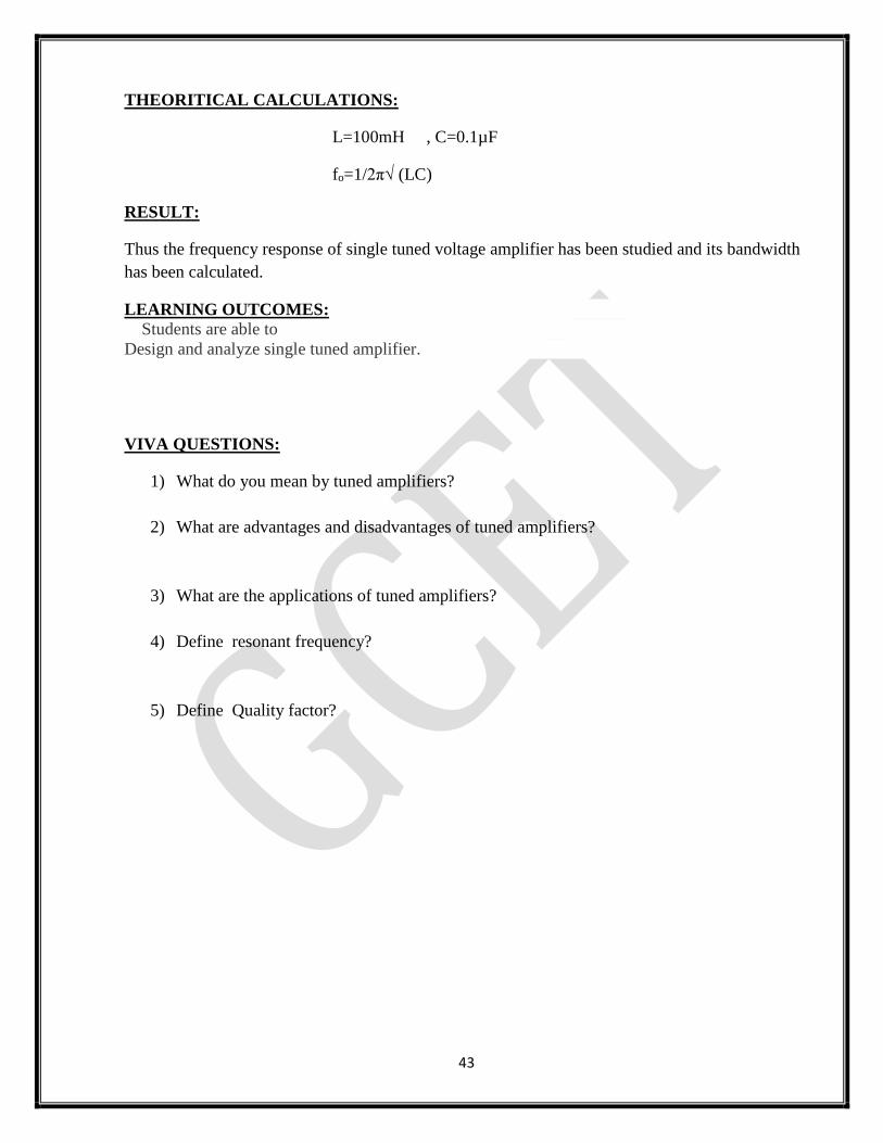
THEORITICAL CALCULATIONS:
L=100mH , C=0.1µF
fo=1/2π√ (LC)
RESULT:
Thus the frequency response of single tuned voltage amplifier has been studied and its bandwidth
has been calculated.
LEARNING OUTCOMES:
Students are able to
Design and analyze single tuned amplifier.
VIVA QUESTIONS:
1) What do you mean by tuned amplifiers?
2) What are advantages and disadvantages of tuned amplifiers?
3) What are the applications of tuned amplifiers?
4) Define resonant frequency?
5) Define Quality factor?
44
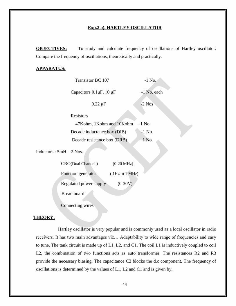
Exp.2 a). HARTLEY OSCILLATOR
OBJECTIVES: To study and calculate frequency of oscillations of Hartley oscillator.
Compare the frequency of oscillations, theoretically and practically.
APPARATUS:
Transistor BC 107 -1 No.
Capacitors 0.1μF, 10 μF -1 No. each
0.22 μF -2 Nos
Resistors
47Kohm, 1Kohm and 10Kohm -1 No.
Decade inductance box (DIB) -1 No.
Decade resistance box (DRB) -1 No.
Inductors : 5mH – 2 Nos.
CRO(Dual Channel ) (0-20 MHz)
Function generator ( 1Hz to 1 MHz)
Regulated power supply (0-30V)
Bread board
Connecting wires
THEORY:
Hartley oscillator is very popular and is commonly used as a local oscillator in radio
receivers. It has two main advantages viz… Adaptability to wide range of frequencies and easy
to tune. The tank circuit is made up of L1, L2, and C1. The coil L1 is inductively coupled to coil
L2, the combination of two functions acts as auto transformer. The resistances R2 and R3
provide the necessary biasing. The capacitance C2 blocks the d.c component. The frequency of
oscillations is determined by the values of L1, L2 and C1 and is given by,
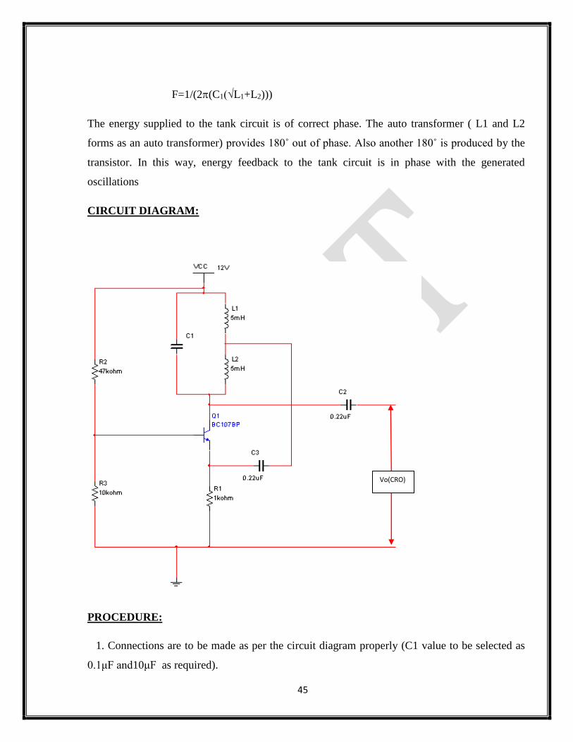
45
F=1/(2(C1(√L1+L2)))
The energy supplied to the tank circuit is of correct phase. The auto transformer ( L1 and L2
forms as an auto transformer) provides 180˚ out of phase. Also another 180˚ is produced by the
transistor. In this way, energy feedback to the tank circuit is in phase with the generated
oscillations
CIRCUIT DIAGRAM:
PROCEDURE:
1. Connections are to be made as per the circuit diagram properly (C1 value to be selected as
0.1μF and10μF as required).
Vo(CRO)

46
2. Connect CRO at output terminals and observe the wave form.
3. Calculate practically the frequency of oscillations by using the expression.
f=1/T, Where T= Time period of the waveform
4. Repeat the above steps 2, 3 for different values of L1 and note down practical values of
oscillations of Hartley oscillator.
5. Compare the values of frequency of oscillations both theoretically and Practically.
OBSERVATIONS:
CAPACITANCE(μF) Theoretical frequency
(KHz)
Practical frequency
(KHz)
MODEL GRAPH:
PRECAUTIONS:
1. All the connections are to be connected properly.
2. Transistor terminals must be identified properly.
47
3. Reading should be taken without any parallax error.
RESULT: Frequency of oscillations is calculated and compared with theoretical values.
LEARNING OUTCOMES:
Students are able to
Design and analyze Hartley oscillator
Viva questions:
1. What are the applications of LC oscillator?
2. What type of feedback is used in oscillators?
3. What is the loop gain of an oscillator?
4. What is the difference between amplifier and oscillator?
5. What is the condition for oscillations?
48
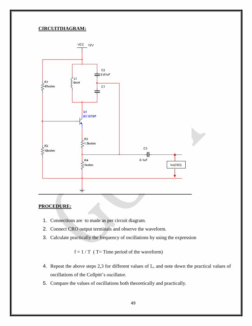
Exp. 2 b).COLPITT’S OSCILLATOR
OBJECTIVE: To study and calculate frequency of oscillations of Colpitt’s oscillator.
APPARATUS:
Transistor BC 107 -1 No.
Capacitors 0.1µF - 1 No.
0.01µF - 2 Nos
Inductor 5mH - 1 No.
Resistors 47KOhm, 1kΩ, 10kΩ, 1.5K -1 No.
Decade inductance box
CRO(Dual Channel ) (0-20 MHz)
Function generator ( 1Hz to 1 MHz)
Regulated power supply (0-30V)
Connecting Wires
THEORY:
The tank circuit is made up of L1,C1 and C2 .The resistance R2 and R3 provides the
necessary biasing. The capacitance C3 blocks the D.C component. The frequency of oscillations
is determined by the values of L1,C4 and C5, and is given by
f = 1 / (2 (CTL1)1/2) Where CT = C1C2 / ( C1 + C2)
The energy supplied to the tank circuit is of in phase. The tank circuit provides 1800 out of
phase. Also the transistor provides another 1800. In this way, energy feedback to the tank circuit
is in phase with the generated oscillations.
49
CIRCUITDIAGRAM:
PROCEDURE:
1. Connections are to made as per circuit diagram.
2. Connect CRO output terminals and observe the waveform.
3. Calculate practically the frequency of oscillations by using the expression
f = 1 / T ( T= Time period of the waveform)
4. Repeat the above steps 2,3 for different values of L, and note down the practical values of
oscillations of the Collpitt’s oscillator.
5. Compare the values of oscillations both theoretically and practically.
Vo(CRO)
50
OBSERVATIONS:
Inductance ( mH ) Theoretical Frequency
( Hz )
Practical Frequency
( Hz )
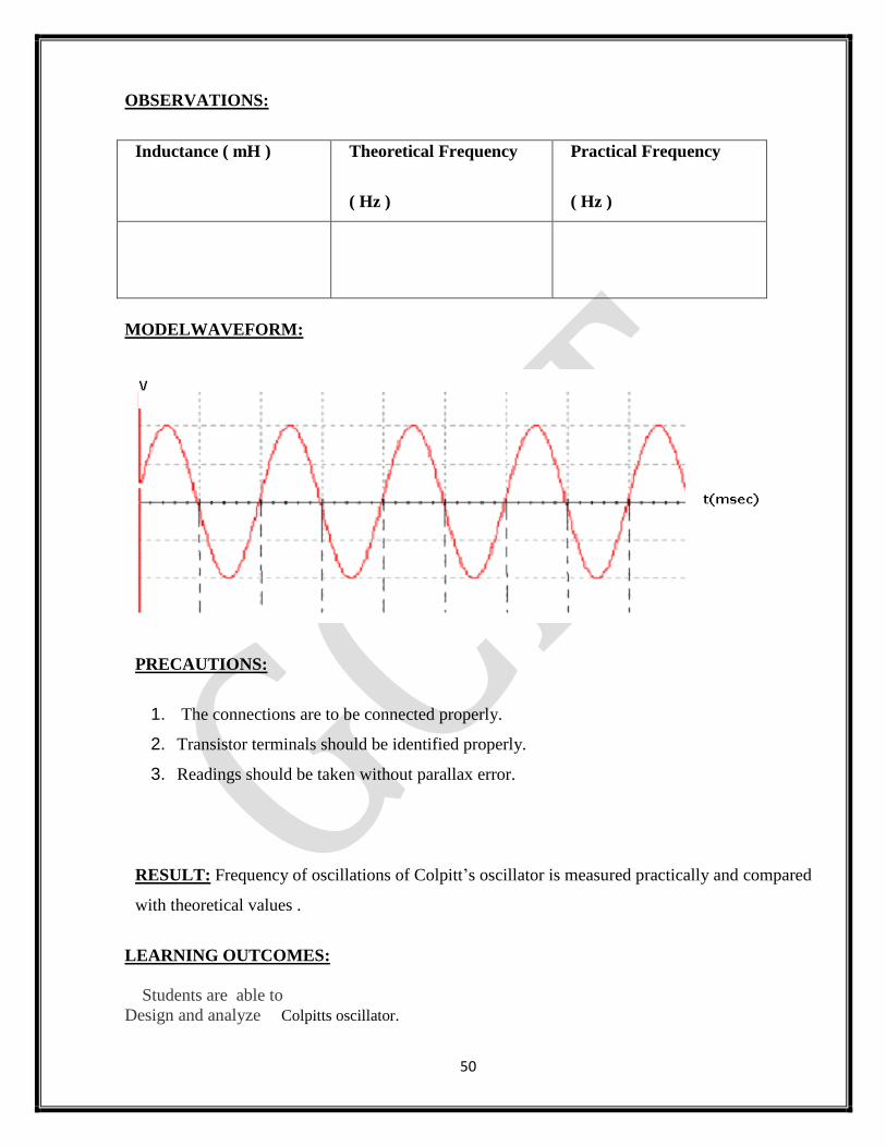
MODELWAVEFORM:
PRECAUTIONS:
1. The connections are to be connected properly.
2. Transistor terminals should be identified properly.
3. Readings should be taken without parallax error.
RESULT: Frequency of oscillations of Colpitt’s oscillator is measured practically and compared
with theoretical values .
LEARNING OUTCOMES:
Students are able to
Design and analyze Colpitts oscillator.
51
VIVA QUESTIONS:
1. What are the applications of LC oscillator?
2. What type of feedback is used in oscillators?
3. What is the loop gain of an oscillator?
4. What is the difference between amplifier and oscillator?
5. What is the condition for oscillations?
52
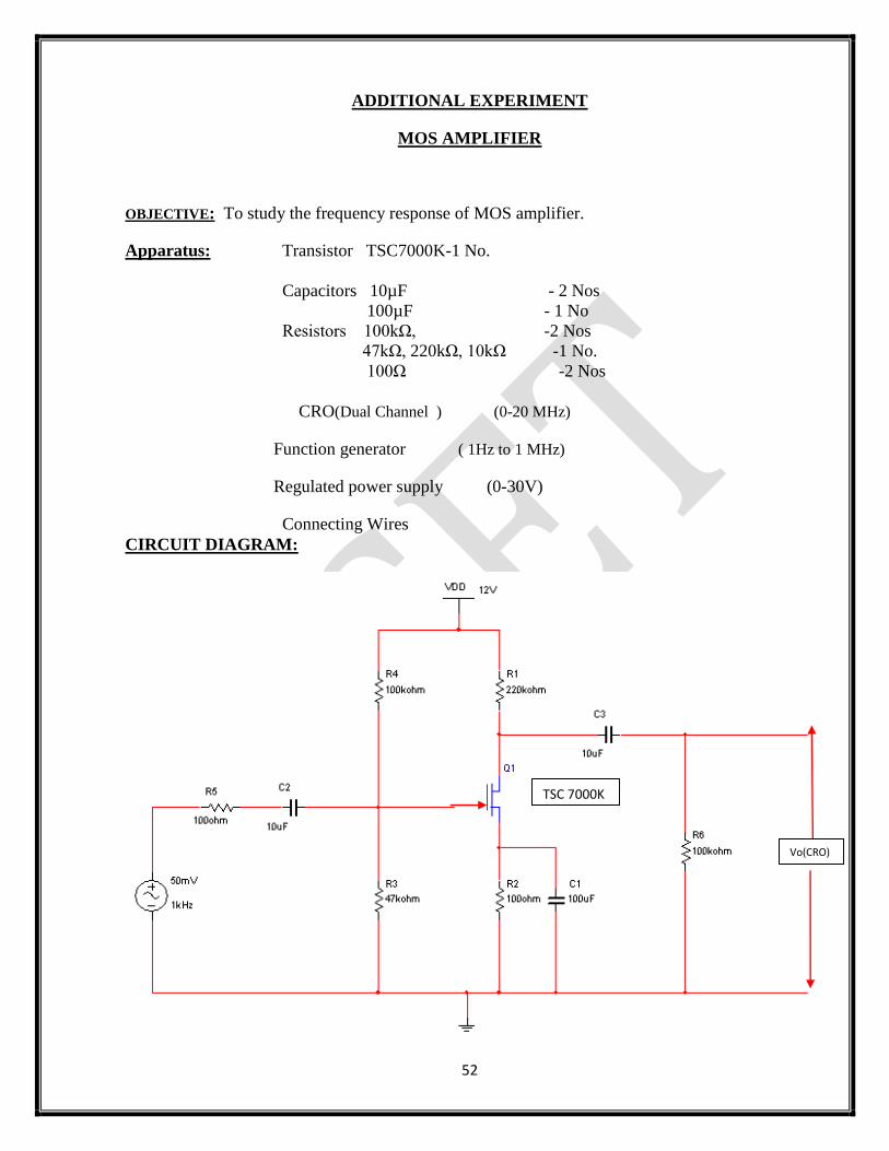
ADDITIONAL EXPERIMENT
MOS AMPLIFIER
OBJECTIVE: To study the frequency response of MOS amplifier.
Apparatus: Transistor TSC7000K-1 No.
Capacitors 10µF - 2 Nos
100µF - 1 No
Resistors 100kΩ, -2 Nos
47kΩ, 220kΩ, 10kΩ -1 No.
100Ω -2 Nos
CRO(Dual Channel ) (0-20 MHz)
Function generator ( 1Hz to 1 MHz)
Regulated power supply (0-30V)
Connecting Wires
CIRCUIT DIAGRAM:
TSC 7000K
Vo(CRO)
53
THEORY:
MOSFET belongs to the family of FET. Its abbreviation is Metal Oxide Semiconductor
Field Effect Transistor. The control terminal is called the gate. Remember that the base terminal
of a bipolar transistor passes a small amount of current. The gate on the FET passes virtually no
current when driven with D.C. When driving the gate with high frequency pulsed D.C. or A.C.
there may be a small amount of current flow. The transistor's "turn on" ( threshold) voltage varies
from one FET to another but is approximately 3.3 volts with respect to the source. When FETs
are used in the audio output section of an amplifier, the VGS (voltage from gate to source) is
rarely higher than 3.5 volts. When FETs are used in switching power supplies, the VGS is usually
much higher (10 to 15 volts). When the gate voltage is above approximately 5 volts, it becomes
more efficient (which means less voltage drop across the FET and therefore less power
dissipation).
MOSFETs are commonly used in electronics circuitry because they are easier to drive in high
current applications (such as the switching power supplies found in car audio amplifiers). If a
bipolar transistor is used, a fraction of the collector/emitter current must flow through the base
junction. In high current situations where there is significant collector/emitter current, the base
current may be significant. FETs can be driven by very little current (compared to the bipolar
transistors). The only current that flows from the drive circuit is the current that flows due to the
capacitance. As you already know, when DC is applied to a capacitor, there is an initial surge then
the current flow stops. When the gate of an FET is driven with a high frequency signal, the drive
circuit essentially sees only a small value capacitor. For low to intermediate frequencies, the drive
circuit has to deliver little current. At very high frequencies or when many FETs are being driven,
the drive circuit must be able to deliver more current.
Note:
The gate of a MOSFET has some capacitance which means that it will hold a charge
(retain voltage). If the gate voltage is not discharged, the FET will continue to conduct current.
This doesn't mean you can charge it and expect the FET to continue to conduct indefinitely but it
will continue to conduct until the voltage on the gate is below the threshold voltage. You can
make sure it turns off if you connect a pull down resistor between the gate and source.
High Current Terminals:
The 'controlled' terminals are called the source and the drain. These are the terminals
responsible for conducting the current through the transistor.
54
PROCEDURE:
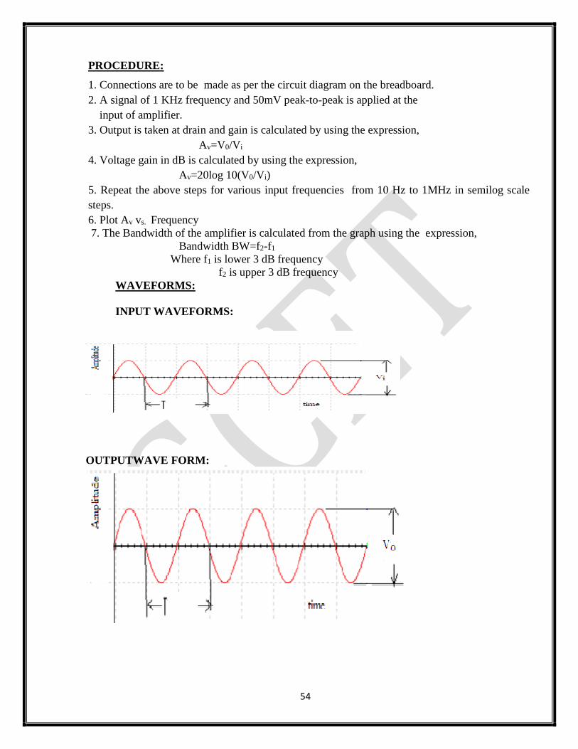
1. Connections are to be made as per the circuit diagram on the breadboard.
2. A signal of 1 KHz frequency and 50mV peak-to-peak is applied at the
input of amplifier.
3. Output is taken at drain and gain is calculated by using the expression,
Av=V0/Vi
4. Voltage gain in dB is calculated by using the expression,
Av=20log 10(V0/Vi)
5. Repeat the above steps for various input frequencies from 10 Hz to 1MHz in semilog scale
steps.
6. Plot Av vs. Frequency
7. The Bandwidth of the amplifier is calculated from the graph using the expression,
Bandwidth BW=f2-f1
Where f1 is lower 3 dB frequency
f2 is upper 3 dB frequency
WAVEFORMS:
INPUT WAVEFORMS:
OUTPUTWAVE FORM:
55
FREQUENCY RESPONSE:
OBSERVATIONS:
Input voltage: 50 mV
S.NO
Frequency(Hz)
OUTPUT
VOLTAGE(V0)
VOLTAGE GAIN
Av= (V0/Vi)
VOLTAGE
GAIN
in dB (20
log10Vo/Vin)
10
50
100
200
400
600
800
1K
5K
10K
50K
100K
200K
400K
600K
800K
1M
RESULT: The voltage gain and frequency response of the MOS amplifier are obtained. Also
gain bandwidth product of the amplifier is calculated.
56
LEARNING OUTCOMES:
Students are able to
Design and analyze MOS amplifiers.
VIVA QUESTIONS:
1) What are the different types of MOSFETS?
2) How is MOSFET different from JFET?
3) What are the advantages of MOSFET?
4) What are the difference between depletion mode MOSFET and enhancement mode
MOSFET ?
57
DESIGN EXPERIMENT
EXP .NO. 1 SHUNT VOLTAGE REGULATOR
OBJECTIVES :
To design a transistorized shunt voltage regulator and observing the regulation action for
i. Different values of input voltages
ii .Different values of load resistors and also to find percentage regulation.
EQUIPMENTS AND COMPONENTS:
APPARATUS REQUIRED: MULTISIM 2007 SOFTWARE
PC
THEORY:
A voltage regulator is a device or a combination of devices, designed to maintain the output
voltage of a power supply as nearly constant as possible even if there are changes in the load or in
input voltage. In shunt voltage regulator, transistor Q1 acts as control element, which is in shunt
with load voltage.
The output voltage is given as
Vo = Vz + VR1 = Vz
The regulation action of the circuit is explained below.
Since Vz is constant, any changes in output voltage reflects a propositional change in R1. If the
output voltage decreases, voltage across R1 decreases which in turn decreases the base voltage of .
As a result the base current of Q1 decreases which allows the load voltage to rise and makes it
constant the same regulation action follows even if the output voltage increases.
CIRCUIT DIAGRAM:

58
PROCEDURE:
i. Connect the circuit as shown in the circuit diagram on bread board..
i. Apply the input voltage from power supply.
ii. For a specific value of load resistor, vary the input voltage from zero to a
maximum of 20 Volts and note the values of output voltage.
iv. Change the load resistor and repeat steps 2 and 3.
v. Remove the load resistor and note down the voltage at no load.
vi. Find percentage regulation.
Percentage load regulation = 100xV
VV
FL
FLNL
vii. Plot the graph for load regulation and line regulation.
OBSERVATIONS:
VOLTAGE AT NO-LOAD =
S.NO
VIN OUTPUT VOLTAGE
RL= RL= RL=
59
CALCULATIONS:
Percentage regulation = 100xV
VV
FL
FLNL
RESULT: Thus the shunt voltage regulator is designed.
What about line regulation??
LEARNING OUTCOMES:
Students are able to
design and analyze shunt voltage regulator .
PRECAUTIONS:
i. Proceed on the experiment only after obtaining expected DC voltages. Do not apply
more than 20 V without connecting load on the output as this would result in
maximum current in shunt transistors.
ii. Shorting the output will result in overheating series resistors which may burn at high
voltage.
iii. Reversing the Zener may not damage the circuit but result in output voltage to drop
2 V or less.
APPLICATIONS:
1. Low current applications.
2. Fixed voltage applications
VIVA QUESTIONS:
1. Define the line regulation?
2. Define load regulation?
3. Mention the applications of shunt voltage regulator?
4. Define a voltage regulator?

60