Future Technology Devices International Ltd...
58
Copyright © 2014 Future Technology Devices International Limited 1 FT900/1/2/3 Embedded Microcontroller Datasheet Version 1.0 Document No.: FT_000965 Clearance No.: FTDI#421 Future Technology Devices International Ltd. FT900/1/2/3 (Embedded Microcontroller) The FT900 series includes the FT900, FT901, FT902 and FT903 which are complete System-On-Chip 32-bit RISC microcontrollers for embedded applications featuring a high level of integration and low power consumption. It has the following features: High performance, low power 32-bit FT32 core processor, running at a frequency of 100MHz. 256kB on-chip Flash memory. 256kB on-chip shadow program memory. True Zero Wait States (0WS) up to 3.1 DMIPS per MHz performance 64kB on-chip data memory. EFUSE for security configuration. Integrated Phase-Locked Loop (PLL) supports external 12MHz crystal and direct external clock source input. 32.768 kHz real time clock support. One USB2.0 EHCI compatible host controller supports high-speed (480 Mbit/s), full-speed (12 Mbit/s), and low-speed (1.5 Mbit/s). One USB2.0 peripheral controller supports high- speed (480 Mbit/s) and full-speed (12 Mbit/s). USB2.0 host and peripheral controllers support the Isochronous, Interrupt, Control, and Bulk transfers. 10/100 Mbps Ethernet that is compliant with the IEEE 802.3/802.3u standards. (FT900 and FT901 only) Support One-Wire debugger download firmware to Flash memory or shadow program memory, and support software debugger. Two CAN controllers support CAN protocol 2.0 parts A & B, data rate is up to 1 Mbit/s. (FT900 and FT902 only) One SPI master supports single / dual / quad modes of data transfer. Clock rate is up to 25 MHz Two SPI slaves support single data transfer with 25MHz clock. Two I 2 C bus interfaces can be configured as master or slave, which support standard / fast / fast plus / high speed mode data transfers. Max data transfer rate up to 3.4 Mbit/s. Clock stretching is supported. I 2 S bus interface can be configured as master or slave. Two clock input options (24.576 MHz and 22.5792 MHz) to support I 2 S master mode for different audio sample rates. UART interface can be configured as one full programmable UART0 or two simple UART0 and UART1 with CTS / RTS control function. Four user timers with pre-scaling and a watchdog function. 8-bit parallel data interface supports camera data capturing. Support 7 independent PWM channels. Channel 0 and 1 can be configured as PCM 8-bit/16-bit stereo audio output. SD host controller is compatible to standard specification V3.0, it supports up to 25 MHz SD clock speed and software supports SD card format in SD/SDHC/SDXC. Support two 10-bit DAC 0/1 channels output, sample rate at ~1 MS/s. Support seven 10-bit ADC 1/7 channels input, sample rate is up to ~960 kS/s. Single 3.3 volt power supply, built-in 1.2 V regulators. 3.3 volt I/O power supply. Support USB Battery Charging Specification Rev 1.2. Downstream port can be configured as SDP, CDP or DCP. Upstream port can perform BCD mode detection. Support VBUS power switching and over current control. Power-On Reset (POR). -40°C to 85°C extended operating temperature range. Available in compact Pb-free 100-Pin packages (all RoHS compliant).
Transcript of Future Technology Devices International Ltd...
Copyright © 2014 Future Technology Devices International Limited 1
FT900/1/2/3 Embedded Microcontroller Datasheet Version 1.0
Document No.: FT_000965 Clearance No.: FTDI#421
Future Technology Devices
International Ltd.
FT900/1/2/3
(Embedded Microcontroller)
The FT900 series includes the FT900,
FT901, FT902 and FT903 which are complete System-On-Chip 32-bit RISC
microcontrollers for embedded applications featuring a high level of
integration and low power consumption. It has the following
features:
High performance, low power 32-bit FT32 core
processor, running at a frequency of 100MHz.
256kB on-chip Flash memory.
256kB on-chip shadow program memory.
True Zero Wait States (0WS) up to 3.1 DMIPS per MHz performance
64kB on-chip data memory.
EFUSE for security configuration.
Integrated Phase-Locked Loop (PLL) supports
external 12MHz crystal and direct external clock source input.
32.768 kHz real time clock support.
One USB2.0 EHCI compatible host controller supports high-speed (480 Mbit/s), full-speed
(12 Mbit/s), and low-speed (1.5 Mbit/s).
One USB2.0 peripheral controller supports high-speed (480 Mbit/s) and full-speed (12 Mbit/s).
USB2.0 host and peripheral controllers support the Isochronous, Interrupt, Control, and Bulk transfers.
10/100 Mbps Ethernet that is compliant with the
IEEE 802.3/802.3u standards. (FT900 and FT901 only)
Support One-Wire debugger download firmware to Flash memory or shadow program memory, and support software debugger.
Two CAN controllers support CAN protocol 2.0 parts A & B, data rate is up to 1 Mbit/s. (FT900
and FT902 only)
One SPI master supports single / dual / quad modes of data transfer. Clock rate is up to 25 MHz
Two SPI slaves support single data transfer with 25MHz clock.
Two I2C bus interfaces can be configured as
master or slave, which support standard / fast / fast plus / high speed mode data transfers.
Max data transfer rate up to 3.4 Mbit/s. Clock stretching is supported.
I2S bus interface can be configured as master or slave. Two clock input options (24.576 MHz
and 22.5792 MHz) to support I2S master mode for different audio sample rates.
UART interface can be configured as one full programmable UART0 or two simple UART0 and UART1 with CTS / RTS control function.
Four user timers with pre-scaling and a watchdog function.
8-bit parallel data interface supports camera data capturing.
Support 7 independent PWM channels. Channel 0 and 1 can be configured as PCM 8-bit/16-bit
stereo audio output.
SD host controller is compatible to standard specification V3.0, it supports up to 25 MHz SD
clock speed and software supports SD card format in SD/SDHC/SDXC.
Support two 10-bit DAC 0/1 channels output, sample rate at ~1 MS/s.
Support seven 10-bit ADC 1/7 channels input, sample rate is up to ~960 kS/s.
Single 3.3 volt power supply, built-in 1.2 V regulators.
3.3 volt I/O power supply.
Support USB Battery Charging Specification Rev 1.2. Downstream port can be configured as
SDP, CDP or DCP. Upstream port can perform BCD mode detection.
Support VBUS power switching and over current control.
Power-On Reset (POR).
-40°C to 85°C extended operating temperature range.
Available in compact Pb-free 100-Pin packages (all RoHS compliant).
Copyright © 2014 Future Technology Devices International Limited 2
FT900/1/2/3 Embedded Microcontroller Datasheet Version 1.0
Document No.: FT_000965 Clearance No.: FTDI#421
Neither the whole nor any part of the information contained in, or the product described in this manual, may be adapted or reproduced in any material or electronic form without the prior written consent of the copyright holder. This product and its documentation are
supplied on an as-is basis and no warranty as to their suitability for any particular purpose is either made or implied. Future Technology
Devices International Ltd will not accept any claim for damages howsoever arising as a result of use or failure of this product. Your
statutory rights are not affected. This product or any variant of it is not intended for use in any medical appliance, device or system in
which the failure of the product might reasonably be expected to result in personal injury. This document provides preliminary
information that may be subject to change without notice. No freedom to use patents or other intellectual property rights is implied by
the publication of this document. Future Technology Devices International Ltd, Unit 1, 2 Seaward Place, Centurion Business Park, Glasgow
G41 1HH United Kingdom. Scotland Registered Company Number: SC136640
Copyright © 2014 Future Technology Devices International Limited 3
FT900/1/2/3 Embedded Microcontroller Datasheet Version 1.0
Document No.: FT_000965 Clearance No.: FTDI#421
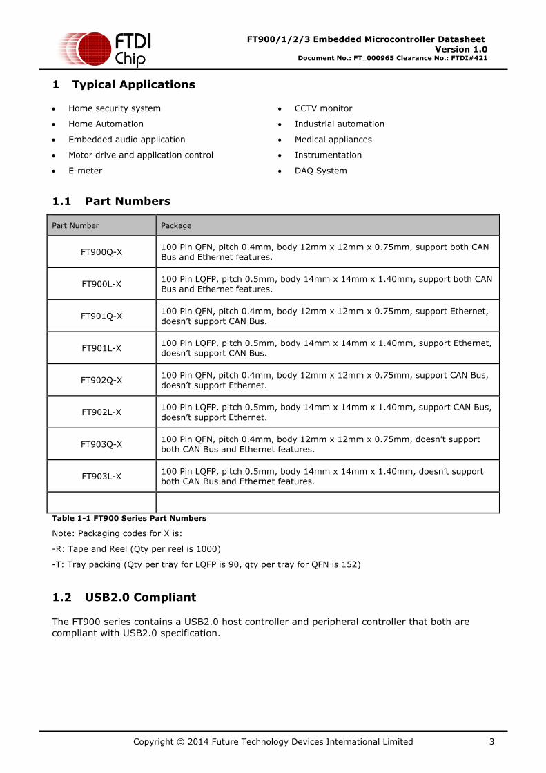
1 Typical Applications
Home security system
Home Automation
Embedded audio application
Motor drive and application control
E-meter
CCTV monitor
Industrial automation
Medical appliances
Instrumentation
DAQ System
1.1 Part Numbers
Part Number Package
FT900Q-X 100 Pin QFN, pitch 0.4mm, body 12mm x 12mm x 0.75mm, support both CAN
Bus and Ethernet features.
FT900L-X 100 Pin LQFP, pitch 0.5mm, body 14mm x 14mm x 1.40mm, support both CAN Bus and Ethernet features.
FT901Q-X 100 Pin QFN, pitch 0.4mm, body 12mm x 12mm x 0.75mm, support Ethernet, doesn’t support CAN Bus.
FT901L-X 100 Pin LQFP, pitch 0.5mm, body 14mm x 14mm x 1.40mm, support Ethernet, doesn’t support CAN Bus.
FT902Q-X 100 Pin QFN, pitch 0.4mm, body 12mm x 12mm x 0.75mm, support CAN Bus, doesn’t support Ethernet.
FT902L-X 100 Pin LQFP, pitch 0.5mm, body 14mm x 14mm x 1.40mm, support CAN Bus,
doesn’t support Ethernet.
FT903Q-X 100 Pin QFN, pitch 0.4mm, body 12mm x 12mm x 0.75mm, doesn’t support both CAN Bus and Ethernet features.
FT903L-X 100 Pin LQFP, pitch 0.5mm, body 14mm x 14mm x 1.40mm, doesn’t support both CAN Bus and Ethernet features.
Table 1-1 FT900 Series Part Numbers
Note: Packaging codes for X is:
-R: Tape and Reel (Qty per reel is 1000)
-T: Tray packing (Qty per tray for LQFP is 90, qty per tray for QFN is 152)
1.2 USB2.0 Compliant
The FT900 series contains a USB2.0 host controller and peripheral controller that both are
compliant with USB2.0 specification.
Copyright © 2014 Future Technology Devices International Limited 4
FT900/1/2/3 Embedded Microcontroller Datasheet Version 1.0
Document No.: FT_000965 Clearance No.: FTDI#421
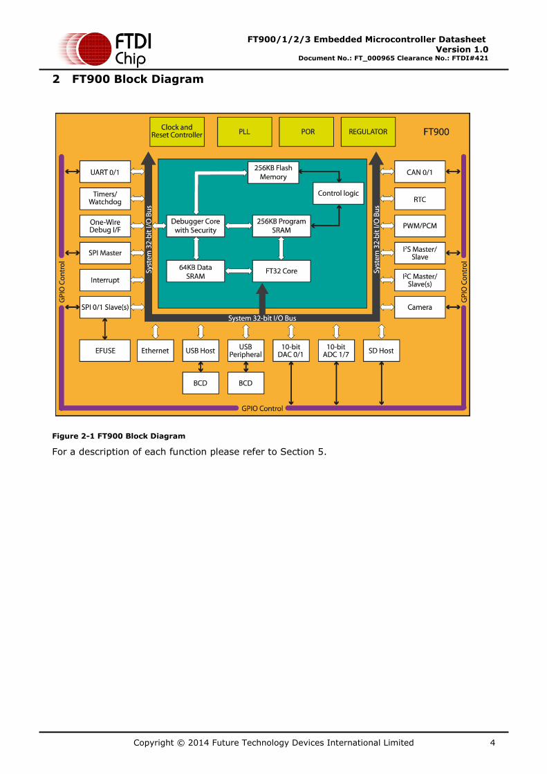
2 FT900 Block Diagram
Figure 2-1 FT900 Block Diagram
For a description of each function please refer to Section 5.
Copyright © 2014 Future Technology Devices International Limited 5
FT900/1/2/3 Embedded Microcontroller Datasheet Version 1.0
Document No.: FT_000965 Clearance No.: FTDI#421
Table of Contents
1 Typical Applications ...................................................................... 3
1.1 Part Numbers...................................................................................... 3
1.2 USB2.0 Compliant ............................................................................... 3
2 FT900 Block Diagram .................................................................... 4
3 Device Pin Out and Signal Description .......................................... 8
3.1 Pin Out – FT900 QFN-100 .................................................................. 8
3.2 Pin Out – FT900 LQFP-100 ............................................................... 12
3.3 Pin Description ................................................................................. 16
4 Function Description................................................................... 24
4.1 Architectural Overview ..................................................................... 24
4.2 FT32 Core Processor ......................................................................... 24
4.3 256kB Flash Memory......................................................................... 24
4.4 Boot Sequence .................................................................................. 24
4.5 Interrupt ........................................................................................... 25
4.6 Memory Mapping .............................................................................. 26
4.7 USB2.0 Host Controller ..................................................................... 27
4.7.1 Features: .................................................................................................................. 27
4.8 USB2.0 Peripheral Contoller .............................................................. 28
4.8.1 Features: .................................................................................................................. 28
4.9 Ethernet Controller ........................................................................... 28
4.9.1 Features: .................................................................................................................. 28
4.10 CAN Bus Controller ......................................................................... 28
4.10.1 Features: .............................................................................................................. 29
4.11 Real Time Clock .............................................................................. 29
4.11.1 Features: .............................................................................................................. 29
4.12 One-Wire Debugger Interface ........................................................ 29
4.12.1 Features: .............................................................................................................. 29
4.13 SPI Interface ................................................................................. 29
4.13.1 Features: .............................................................................................................. 29
4.14 I2C Interface .................................................................................. 30
4.14.1 Features: .............................................................................................................. 30
4.15 UART Interface .............................................................................. 30
4.15.1 Features: .............................................................................................................. 30
4.16 Timers and Watchdog Timer .......................................................... 31
4.16.1 Features: .............................................................................................................. 31
4.17 I2S Interface .................................................................................. 31
Copyright © 2014 Future Technology Devices International Limited 6
FT900/1/2/3 Embedded Microcontroller Datasheet Version 1.0
Document No.: FT_000965 Clearance No.: FTDI#421
4.17.1 Features: .............................................................................................................. 31
4.18 Camera Parallel Interface (Data Capture) ...................................... 31
4.18.1 Features: .............................................................................................................. 32
4.19 PWM............................................................................................... 32
4.19.1 Features: .............................................................................................................. 32
4.20 SD host controller .......................................................................... 32
4.20.1 Features: .............................................................................................................. 32
4.21 Analog to Digital Converter (ADC) ................................................. 33
4.21.1 Features: .............................................................................................................. 33
4.22 Digital to Analog Converter (DAC) ................................................. 33
4.22.1 Features: .............................................................................................................. 33
4.23 General Purpose Input Output ....................................................... 33
4.23.1 Features: .............................................................................................................. 34
4.24 System Clocks ................................................................................ 34
4.24.1 12 MHz Oscillator ................................................................................................... 34
4.24.2 Phase Locked Loop ................................................................................................ 34
4.24.3 32.768 KHz RTC Oscillator ....................................................................................... 34
4.24.4 Internal Slow Clock Oscillator ................................................................................... 34
4.25 Power Management ....................................................................... 34
4.25.1 Power Supply ......................................................................................................... 34
4.25.2 Power Down Mode .................................................................................................. 35
5 Devices Characteristics and Ratings ........................................... 36
5.1 Absolute Maximum Ratings............................................................... 36
5.2 DC Characteristics............................................................................. 37
5.3 AC Characteristics ............................................................................. 42
6 Application Information ............................................................. 44
6.1 Crystal Oscillator .............................................................................. 44
6.1.1 Crystal oscillator application circuit .............................................................................. 44
6.1.2 External clock input.................................................................................................... 44
6.2 RTC Oscillator ................................................................................... 44
6.3 Standard I/O Pin Configuration ........................................................ 45
6.4 USB2.0 Peripheral and Host Interface .............................................. 46
6.5 10/100 Mb/s Ethernet Interface ...................................................... 47
7 Package Parameters ................................................................... 48
7.1 QFN-100 Package Dimensions .......................................................... 48
7.2 QFN-100 Device Marking .................................................................. 49
7.2.1 FT90XQ Top Side ....................................................................................................... 49
7.3 LQFP-100 Package Dimensions ......................................................... 50
7.4 LQFP-100 Device Marking ................................................................. 51
Copyright © 2014 Future Technology Devices International Limited 7
FT900/1/2/3 Embedded Microcontroller Datasheet Version 1.0
Document No.: FT_000965 Clearance No.: FTDI#421
7.4.1 FT90XL Top Side ........................................................................................................ 51
7.5 Solder Reflow Profile ........................................................................ 52
8 Abbreviations ............................................................................. 53
9 FTDI Chip Contact Information ................................................... 55
Appendix A – References ........................................................................... 56
Appendix B - List of Figures and Tables ..................................................... 56
Appendix C - Revision History .................................................................... 58
Copyright © 2014 Future Technology Devices International Limited 8
FT900/1/2/3 Embedded Microcontroller Datasheet Version 1.0
Document No.: FT_000965 Clearance No.: FTDI#421
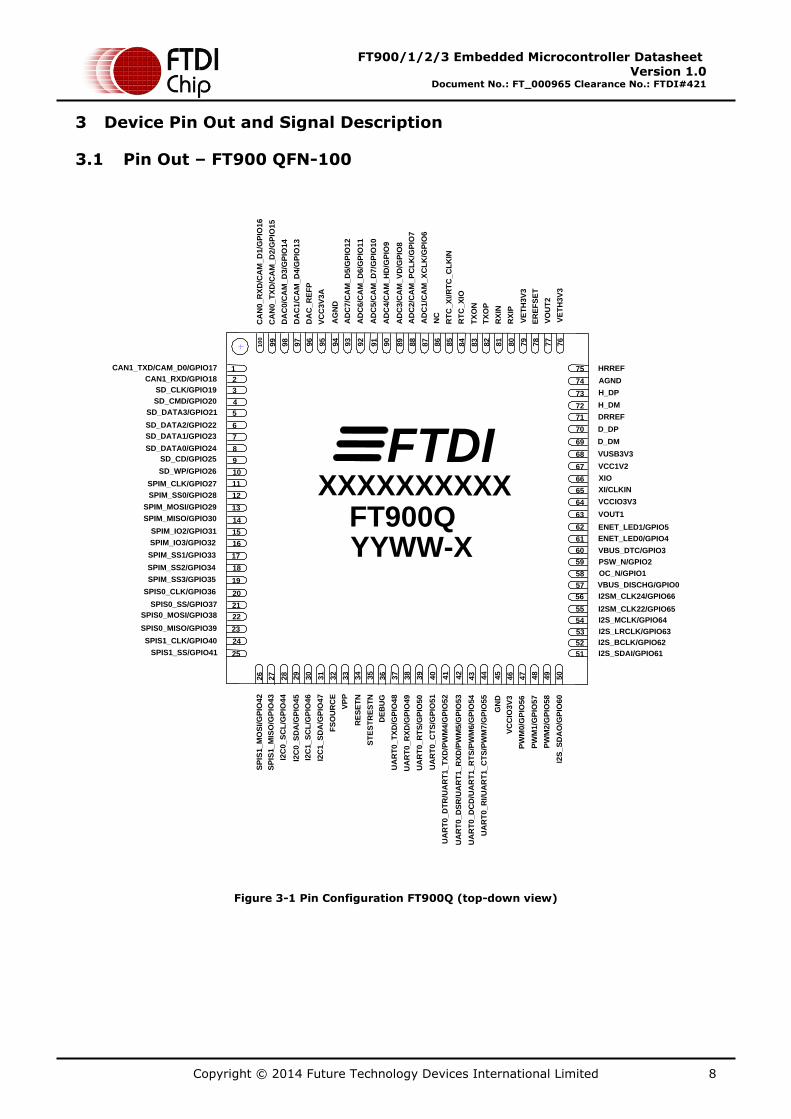
3 Device Pin Out and Signal Description
3.1 Pin Out – FT900 QFN-100
2
1
4
3
5
7
6
8
9
11
10
12
SD_DATA3/GPIO21
SD_DATA2/GPIO22
SD_DATA1/GPIO23
SD_DATA0/GPIO24
SD_CD/GPIO25
SD_WP/GPIO26
SPIM_CLK/GPIO27
SPIM_SS0/GPIO28
13
15
14
16
CAN1_TXD/CAM_D0/GPIO17
CAN1_RXD/GPIO18
SD_CLK/GPIO19
SD_CMD/GPIO20
SPIM_MOSI/GPIO29
SPIM_MISO/GPIO30
SPIM_IO2/GPIO31
SPIM_IO3/GPIO32
I2C
0_
SC
L/G
PIO
44
I2C
0_
SD
A/G
PIO
45
I2C
1_
SC
L/G
PIO
46
I2C
1_
SD
A/G
PIO
47
UA
RT
0_
RT
S/G
PIO
50
26
27
SP
IS1
_M
OS
I/G
PIO
42
SP
IS1
_M
ISO
/GP
IO4
3
FS
OU
RC
E
VP
P
UA
RT
0_
CT
S/G
PIO
51
UA
RT
0_
DT
R/U
AR
T1
_T
XD
/PW
M4
/GP
IO5
2
57
55
56
54
VUSB3V3
VCCIO3V3
D_DM
D_DP
DRREF
H_DM
AGND
HRREF
RX
IN
RX
IP
VC
C3
V3
A
TX
ON
NC
AD
C2
/CA
M_
PC
LK
/GP
IO7
DA
C_
RE
FP
DA
C1/C
AM
_D
4/G
PIO
13
FTDIXXXXXXXXXX
FT900QYYWW-X
VOUT1
XI/CLKIN
AD
C4
/CA
M_
HD
/GP
IO9
RT
C_
XI/R
TC
_C
LK
IN
DA
C0
/CA
M_
D3
/GP
IO1
4
TX
OP
RT
C_
XIO
AD
C1/C
AM
_X
CL
K/G
PIO
6
AD
C3
/CA
M_
VD
/GP
IO8
AG
ND
28
29
30
31
32
33
34
35
36
37
38
39
40
41
10
0
17
18
19
42
43
44
52
53
51
SPIM_SS1/GPIO33
SPIM_SS2/GPIO34
SPIM_SS3/GPIO35
RE
SE
TN
ST
ES
TR
ES
TN
DE
BU
G
UA
RT
0_
TX
D/G
PIO
48
UA
RT
0_
RX
D/G
PIO
49
UA
RT
0_
DS
R/U
AR
T1
_R
XD
/PW
M5
/GP
IO5
3
UA
RT
0_
DC
D/U
AR
T1
_R
TS
/PW
M6
/GP
IO5
4
UA
RT
0_
RI/U
AR
T1
_C
TS
/PW
M7
/GP
IO5
5
OC_N/GPIO1
PSW_N/GPIO2
VBUS_DTC/GPIO3
ENET_LED0/GPIO4
ENET_LED1/GPIO5
XIO
VCC1V2
H_DP
VO
UT
2
VE
TH
3V
3
GN
D
VC
CIO
3V
3
PW
M0
/GP
IO5
6
45
46
47
48
49
50
PW
M1
/GP
IO5
7
PW
M2
/GP
IO5
8
I2S
_S
DA
O/G
PIO
60
21
20
22
SPIS0_CLK/GPIO36
SPIS0_SS/GPIO37
SPIS0_MOSI/GPIO38
23
24
25
SPIS0_MISO/GPIO39
SPIS1_CLK/GPIO40
SPIS1_SS/GPIO41
VBUS_DISCHG/GPIO0
58
59
60
61
62
63
64
65
66
67
68
69
70
71
72
73
74
75
I2SM_CLK24/GPIO66
I2SM_CLK22/GPIO65
I2S_MCLK/GPIO64
I2S_LRCLK/GPIO63
I2S_BCLK/GPIO62
I2S_SDAI/GPIO61
99
98
97
96
95
94
93
92
91
90
89
88
87
86
84
85
82
83
80
81
78
79
77
76
VE
TH
3V
3
ER
EF
SE
T
AD
C5
/CA
M_
D7
/GP
IO1
0
CA
N0
_T
XD
/CA
M_
D2/G
PIO
15
AD
C6
/CA
M_
D6
/GP
IO1
1
AD
C7
/CA
M_
D5
/GP
IO1
2
CA
N0
_R
XD
/CA
M_
D1
/GP
IO1
6
Figure 3-1 Pin Configuration FT900Q (top-down view)
Copyright © 2014 Future Technology Devices International Limited 9
FT900/1/2/3 Embedded Microcontroller Datasheet Version 1.0
Document No.: FT_000965 Clearance No.: FTDI#421
2
1
4
3
5
7
6
8
9
11
10
12
SD_DATA3/GPIO21
SD_DATA2/GPIO22
SD_DATA1/GPIO23
SD_DATA0/GPIO24
SD_CD/GPIO25
SD_WP/GPIO26
SPIM_CLK/GPIO27
SPIM_SS0/GPIO28
13
15
14
16
CAM_D0/GPIO17
GPIO18
SD_CLK/GPIO19
SD_CMD/GPIO20
SPIM_MOSI/GPIO29
SPIM_MISO/GPIO30
SPIM_IO2/GPIO31
SPIM_IO3/GPIO32
I2C
0_
SC
L/G
PIO
44
I2C
0_S
DA
/GP
IO4
5
I2C
1_
SC
L/G
PIO
46
I2C
1_
SD
A/G
PIO
47
UA
RT
0_
RT
S/G
PIO
50
26
27
SP
IS1
_M
OS
I/G
PIO
42
SP
IS1
_M
ISO
/GP
IO4
3
FS
OU
RC
E
VP
P
UA
RT
0_
CT
S/G
PIO
51
UA
RT
0_
DT
R/U
AR
T1
_T
XD
/PW
M4
/GP
IO5
2
57
55
56
54
VUSB3V3
VCCIO3V3
D_DM
D_DP
DRREF
H_DM
AGND
HRREF
RX
IN
RX
IP
VC
C3
V3
A
TX
ON
NC
AD
C2
/CA
M_
PC
LK
/GP
IO7
DA
C_
RE
FP
DA
C1
/CA
M_
D4
/GP
IO1
3
FTDIXXXXXXXXXX
FT901QYYWW-X
VOUT1
XI/CLKIN
AD
C4
/CA
M_
HD
/GP
IO9
RT
C_
XI/R
TC
_C
LK
IN
DA
C0
/CA
M_
D3
/GP
IO1
4
TX
OP
RT
C_
XIO
AD
C1
/CA
M_
XC
LK
/GP
IO6
AD
C3
/CA
M_
VD
/GP
IO8
AG
ND
28
29
30
31
32
33
34
35
36
37
38
39
40
41
10
0
17
18
19
42
43
44
52
53
51
SPIM_SS1/GPIO33
SPIM_SS2/GPIO34
SPIM_SS3/GPIO35
RE
SE
TN
ST
ES
TR
ES
TN
DE
BU
G
UA
RT
0_
TX
D/G
PIO
48
UA
RT
0_
RX
D/G
PIO
49
UA
RT
0_
DS
R/U
AR
T1
_R
XD
/PW
M5
/GP
IO5
3
UA
RT
0_
DC
D/U
AR
T1
_R
TS
/PW
M6/G
PIO
54
UA
RT
0_
RI/U
AR
T1
_C
TS
/PW
M7/G
PIO
55
OC_N/GPIO1
PSW_N/GPIO2
VBUS_DTC/GPIO3
ENET_LED0/GPIO4
ENET_LED1/GPIO5
XIO
VCC1V2
H_DP
VO
UT
2
VE
TH
3V
3
GN
D
VC
CIO
3V
3
PW
M0
/GP
IO5
6
45
46
47
48
49
50
PW
M1
/GP
IO5
7
PW
M2
/GP
IO5
8
I2S
_S
DA
O/G
PIO
60
21
20
22
SPIS0_CLK/GPIO36
SPIS0_SS/GPIO37
SPIS0_MOSI/GPIO38
23
24
25
SPIS0_MISO/GPIO39
SPIS1_CLK/GPIO40
SPIS1_SS/GPIO41
VBUS_DISCHG/GPIO0
58
59
60
61
62
63
64
65
66
67
68
69
70
71
72
73
74
75
I2SM_CLK24/GPIO66
I2SM_CLK22/GPIO65
I2S_MCLK/GPIO64
I2S_LRCLK/GPIO63
I2S_BCLK/GPIO62
I2S_SDAI/GPIO61
99
98
97
96
95
94
93
92
91
90
89
88
87
86
84
85
82
83
80
81
78
79
77
76
VE
TH
3V
3
ER
EF
SE
T
AD
C5
/CA
M_
D7
/GP
IO1
0
CA
M_
D2
/GP
IO1
5
AD
C6
/CA
M_
D6
/GP
IO1
1
AD
C7
/CA
M_
D5
/GP
IO1
2
CA
M_
D1
/GP
IO1
6
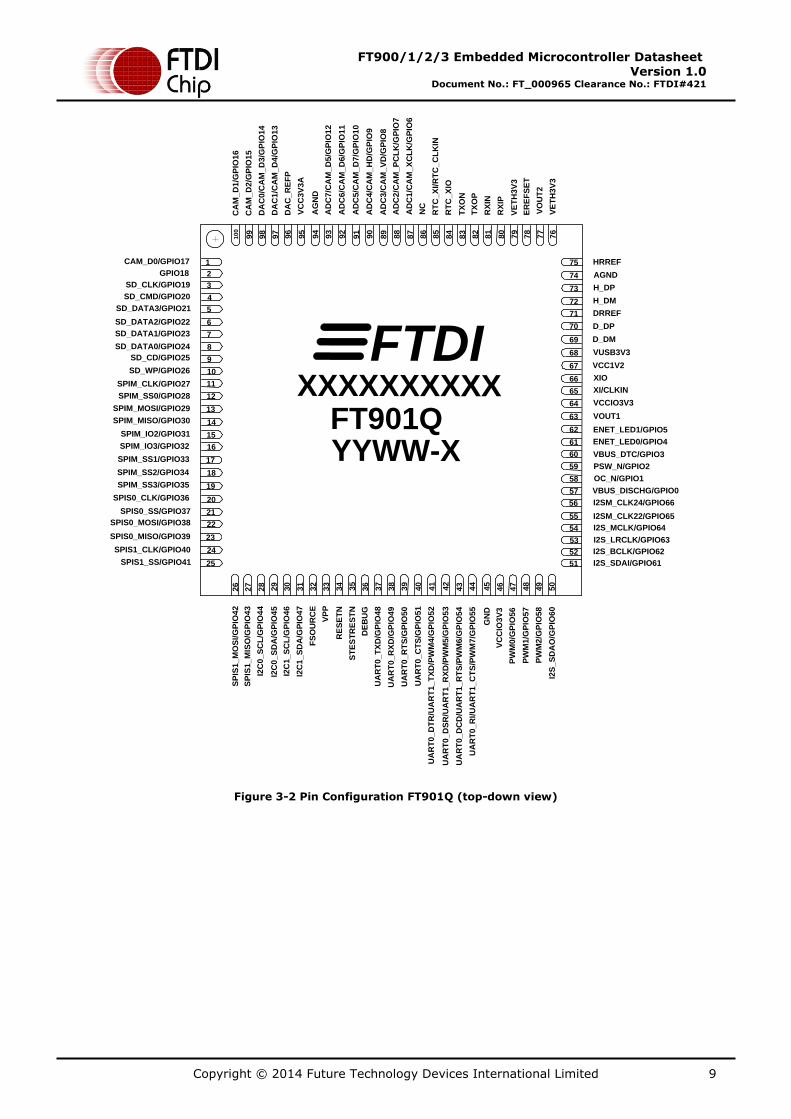
Figure 3-2 Pin Configuration FT901Q (top-down view)
Copyright © 2014 Future Technology Devices International Limited 10
FT900/1/2/3 Embedded Microcontroller Datasheet Version 1.0
Document No.: FT_000965 Clearance No.: FTDI#421
2
1
4
3
5
7
6
8
9
11
10
12
SD_DATA3/GPIO21
SD_DATA2/GPIO22
SD_DATA1/GPIO23
SD_DATA0/GPIO24
SD_CD/GPIO25
SD_WP/GPIO26
SPIM_CLK/GPIO27
SPIM_SS0/GPIO28
13
15
14
16
CAN1_TXD/CAM_D0/GPIO17
CAN1_RXD/GPIO18
SD_CLK/GPIO19
SD_CMD/GPIO20
SPIM_MOSI/GPIO29
SPIM_MISO/GPIO30
SPIM_IO2/GPIO31
SPIM_IO3/GPIO32
I2C
0_
SC
L/G
PIO
44
I2C
0_
SD
A/G
PIO
45
I2C
1_
SC
L/G
PIO
46
I2C
1_
SD
A/G
PIO
47
UA
RT
0_
RT
S/G
PIO
50
26
27
SP
IS1
_M
OS
I/G
PIO
42
SP
IS1
_M
ISO
/GP
IO4
3
FS
OU
RC
E
VP
P
UA
RT
0_
CT
S/G
PIO
51
UA
RT
0_
DT
R/U
AR
T1
_T
XD
/PW
M4
/GP
IO5
2
57
55
56
54
VUSB3V3
VCCIO3V3
D_DM
D_DP
DRREF
H_DM
AGND
HRREF
NC
NC
VC
C3
V3
A
NC
NC
AD
C2
/CA
M_
PC
LK
/GP
IO7
DA
C_
RE
FP
DA
C1/C
AM
_D
4/G
PIO
13
FTDIXXXXXXXXXX
FT902QYYWW-X
VOUT1
XI/CLKINA
DC
4/C
AM
_H
D/G
PIO
9
RT
C_
XI/R
TC
_C
LK
IN
DA
C0
/CA
M_
D3
/GP
IO1
4
NC
RT
C_
XIO
AD
C1/C
AM
_X
CL
K/G
PIO
6
AD
C3
/CA
M_
VD
/GP
IO8
AG
ND
28
29
30
31
32
33
34
35
36
37
38
39
40
41
10
0
17
18
19
42
43
44
52
53
51
SPIM_SS1/GPIO33
SPIM_SS2/GPIO34
SPIM_SS3/GPIO35
RE
SE
TN
ST
ES
TR
ES
TN
DE
BU
G
UA
RT
0_
TX
D/G
PIO
48
UA
RT
0_
RX
D/G
PIO
49
UA
RT
0_
DS
R/U
AR
T1
_R
XD
/PW
M5
/GP
IO5
3
UA
RT
0_
DC
D/U
AR
T1
_R
TS
/PW
M6
/GP
IO5
4
UA
RT
0_
RI/U
AR
T1
_C
TS
/PW
M7
/GP
IO5
5
OC_N/GPIO1
PSW_N/GPIO2
VBUS_DTC/GPIO3
GPIO4
GPIO5
XIO
VCC1V2
H_DP
NC
NC
GN
D
VC
CIO
3V
3
PW
M0
/GP
IO5
6
45
46
47
48
49
50
PW
M1
/GP
IO5
7
PW
M2
/GP
IO5
8
I2S
_S
DA
O/G
PIO
60
21
20
22
SPIS0_CLK/GPIO36
SPIS0_SS/GPIO37
SPIS0_MOSI/GPIO38
23
24
25
SPIS0_MISO/GPIO39
SPIS1_CLK/GPIO40
SPIS1_SS/GPIO41
VBUS_DISCHG/GPIO0
58
59
60
61
62
63
64
65
66
67
68
69
70
71
72
73
74
75
I2SM_CLK24/GPIO66
I2SM_CLK22/GPIO65
I2S_MCLK/GPIO64
I2S_LRCLK/GPIO63
I2S_BCLK/GPIO62
I2S_SDAI/GPIO61
99
98
97
96
95
94
93
92
91
90
89
88
87
86
84
85
82
83
80
81
78
79
77
76
NC
NC
AD
C5
/CA
M_
D7
/GP
IO1
0
CA
N0
_T
XD
/CA
M_
D2/G
PIO
15
AD
C6
/CA
M_
D6
/GP
IO1
1
AD
C7
/CA
M_
D5
/GP
IO1
2
CA
N0
_R
XD
/CA
M_
D1
/GP
IO1
6
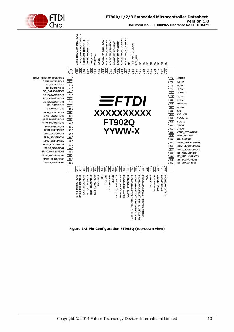
Figure 3-3 Pin Configuration FT902Q (top-down view)

Copyright © 2014 Future Technology Devices International Limited 11
FT900/1/2/3 Embedded Microcontroller Datasheet Version 1.0
Document No.: FT_000965 Clearance No.: FTDI#421
2
1
4
3
5
7
6
8
9
11
10
12
SD_DATA3/GPIO21
SD_DATA2/GPIO22
SD_DATA1/GPIO23
SD_DATA0/GPIO24
SD_CD/GPIO25
SD_WP/GPIO26
SPIM_CLK/GPIO27
SPIM_SS0/GPIO28
13
15
14
16
CAM_D0/GPIO17
GPIO18
SD_CLK/GPIO19
SD_CMD/GPIO20
SPIM_MOSI/GPIO29
SPIM_MISO/GPIO30
SPIM_IO2/GPIO31
SPIM_IO3/GPIO32
I2C
0_
SC
L/G
PIO
44
I2C
0_S
DA
/GP
IO4
5
I2C
1_
SC
L/G
PIO
46
I2C
1_
SD
A/G
PIO
47
UA
RT
0_
RT
S/G
PIO
50
26
27
SP
IS1
_M
OS
I/G
PIO
42
SP
IS1
_M
ISO
/GP
IO4
3
FS
OU
RC
E
VP
P
UA
RT
0_
CT
S/G
PIO
51
UA
RT
0_
DT
R/U
AR
T1
_T
XD
/PW
M4
/GP
IO5
2
57
55
56
54
VUSB3V3
VCCIO3V3
D_DM
D_DP
DRREF
H_DM
AGND
HRREF
NC
NC
VC
C3
V3
A
NC
NC
AD
C2
/CA
M_
PC
LK
/GP
IO7
DA
C_
RE
FP
DA
C1
/CA
M_
D4
/GP
IO1
3
FTDIXXXXXXXXXX
FT903QYYWW-X
VOUT1
XI/CLKIN
AD
C4
/CA
M_
HD
/GP
IO9
RT
C_
XI/R
TC
_C
LK
IN
DA
C0
/CA
M_
D3
/GP
IO1
4
NC
RT
C_
XIO
AD
C1
/CA
M_
XC
LK
/GP
IO6
AD
C3
/CA
M_
VD
/GP
IO8
AG
ND
28
29
30
31
32
33
34
35
36
37
38
39
40
41
10
0
17
18
19
42
43
44
52
53
51
SPIM_SS1/GPIO33
SPIM_SS2/GPIO34
SPIM_SS3/GPIO35
RE
SE
TN
ST
ES
TR
ES
TN
DE
BU
G
UA
RT
0_
TX
D/G
PIO
48
UA
RT
0_
RX
D/G
PIO
49
UA
RT
0_
DS
R/U
AR
T1
_R
XD
/PW
M5
/GP
IO5
3
UA
RT
0_
DC
D/U
AR
T1
_R
TS
/PW
M6/G
PIO
54
UA
RT
0_
RI/U
AR
T1
_C
TS
/PW
M7/G
PIO
55
OC_N/GPIO1
PSW_N/GPIO2
VBUS_DTC/GPIO3
GPIO4
GPIO5
XIO
VCC1V2
H_DP
NC
NC
GN
D
VC
CIO
3V
3
PW
M0
/GP
IO5
6
45
46
47
48
49
50
PW
M1
/GP
IO5
7
PW
M2
/GP
IO5
8
I2S
_S
DA
O/G
PIO
60
21
20
22
SPIS0_CLK/GPIO36
SPIS0_SS/GPIO37
SPIS0_MOSI/GPIO38
23
24
25
SPIS0_MISO/GPIO39
SPIS1_CLK/GPIO40
SPIS1_SS/GPIO41
VBUS_DISCHG/GPIO0
58
59
60
61
62
63
64
65
66
67
68
69
70
71
72
73
74
75
I2SM_CLK24/GPIO66
I2SM_CLK22/GPIO65
I2S_MCLK/GPIO64
I2S_LRCLK/GPIO63
I2S_BCLK/GPIO62
I2S_SDAI/GPIO61
99
98
97
96
95
94
93
92
91
90
89
88
87
86
84
85
82
83
80
81
78
79
77
76
NC
NC
AD
C5
/CA
M_
D7
/GP
IO1
0
CA
M_
D2
/GP
IO1
5
AD
C6
/CA
M_
D6
/GP
IO1
1
AD
C7
/CA
M_
D5
/GP
IO1
2
CA
M_
D1
/GP
IO1
6
Figure 3-4 Pin Configuration FT903Q (top-down view)
Copyright © 2014 Future Technology Devices International Limited 12
FT900/1/2/3 Embedded Microcontroller Datasheet Version 1.0
Document No.: FT_000965 Clearance No.: FTDI#421
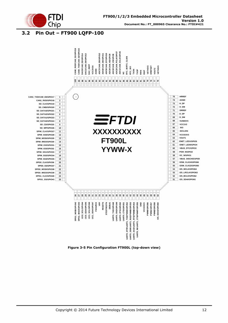
3.2 Pin Out – FT900 LQFP-100
CA
N0_
RX
D/C
AM
_D
1/G
PIO
16
CA
N0_
TX
D/C
AM
_D
2/G
PIO
15
DA
C0/C
AM
_D
3/G
PIO
14
DA
C1/C
AM
_D
4/G
PIO
13
DA
C_
RE
FP
AG
ND
AD
C7/C
AM
_D
5/G
PIO
12
ER
EF
SE
T
RX
IP
RX
IN
TX
OP
TX
ON
RT
C_
XIO
RT
C_
XI/
RT
C_
CL
KIN
NC
AD
C1/C
AM
_X
CL
K/G
PIO
6
AD
C2/C
AM
_P
CL
K/G
PIO
7
AD
C3/C
AM
_V
D/G
PIO
8
AD
C4/C
AM
_H
D/G
PIO
9
AD
C5/C
AM
_D
7/G
PIO
10
AD
C6/C
AM
_D
6/G
PIO
11
10
0
85
86
87
88
89
90
91
92
93
94
95
96
97
98
99
76
77
78
79
80
81
82
83
84
36
35
34
33
32
31
30
29
28
27
26
48
47
46
45
44
43
42
41
40
39
38
37
49
50
SP
IS1_
MO
SI/
GP
IO4
2
SP
IS1
_M
ISO
/GP
IO4
3
I2C
0_
SC
L/G
PIO
44
I2C
0_
SD
A/G
PIO
45
I2C
1_
SC
L/G
PIO
46
I2C
1_
SD
A/G
PIO
47
FS
OU
RC
E
VP
P
RE
SE
TN
ST
ES
TR
ES
TN
DE
BU
G
UA
RT
0_
TX
D/G
PIO
48
UA
RT
0_
RX
D/G
PIO
49
UA
RT
0_
RT
S/G
PIO
50
UA
RT
0_
CT
S/G
PIO
51
UA
RT
0_
DT
R/U
AR
T1_
TX
D/P
WM
4/G
PIO
52
UA
RT
0_
DS
R/U
AR
T1_
RX
D/P
WM
5/G
PIO
53
UA
RT
0_
DC
D/U
AR
T1
_R
TS
/PW
M6/G
PIO
54
UA
RT
0_
RI/
UA
RT
1_
CT
S/P
WM
7/G
PIO
55
GN
D
PW
M0/G
PIO
56
PW
M1/G
PIO
57
PW
M2/G
PIO
58
I2S
_S
DA
O/G
PIO
60
2
3
4
5
6
7
8
9
10
11
12
13
14
15
16
1
24
25
17
18
19
20
21
22
23
SPIS1_SS/GPIO41
SPIS1_CLK/GPIO40
SPIS0_MISO/GPIO39
SPIS0_MOSI/GPIO38
SPIS0_SS/GPIO37
SPIS0_CLK/GPIO36
SPIM_SS3/GPIO35
SPIM_SS2/GPIO34
SPIM_SS1/GPIO33
SPIM_IO3/GPIO32
SPIM_IO2/GPIO31
SPIM_MISO/GPIO30
SPIM_MOSI/GPIO29
SPIM_SS0/GPIO28
SPIM_CLK/GPIO27
SD_WP/GPIO26
SD_CD/GPIO25
SD_DATA0/GPIO24
SD_DATA1/GPIO23
SD_DATA2/GPIO22
SD_DATA3/GPIO21
SD_CMD/GPIO20
SD_CLK/GPIO19
CAN1_TXD/CAM_D0/GPIO17
CAN1_RXD/GPIO18
HRREF
AGND
H_DP
H_DM
DRREF
D_DP
D_DM
VCC1V2
XIO
XI/CLKIN
ENET_LED1/GPIO5
ENET_LED0/GPIO4
VBUS_DTC/GPIO3
PSW_N/GPIO2
OC_N/GPIO1
VBUS_ DISCHG/ GPIO0
I2SM_CLK24/GPIO66
I2SM_CLK22/GPIO65
I2S_MCLK/GPIO64
I2S_LRCLK/GPIO63
I2S_BCLK/GPIO62
I2S_SDAI/GPIO61
60
61
62
63
64
65
66
67
68
69
70
71
72
73
74
75
51
52
53
54
55
56
57
58
59
FTDIXXXXXXXXXX
FT900L
YYWW-XV
CC
IO3
V3
VCCIO3V3
VUSB3V3
VOUT1
VO
UT
2
VC
C3
V3
A
VE
TH
3V
3
VE
TH
3V
3
Figure 3-5 Pin Configuration FT900L (top-down view)
Copyright © 2014 Future Technology Devices International Limited 13
FT900/1/2/3 Embedded Microcontroller Datasheet Version 1.0
Document No.: FT_000965 Clearance No.: FTDI#421
CA
M_D
1/G
PIO
16
CA
M_
D2/G
PIO
15
DA
C0/C
AM
_D
3/G
PIO
14
DA
C1/C
AM
_D
4/G
PIO
13
DA
C_
RE
FP
AG
ND
AD
C7/C
AM
_D
5/G
PIO
12
ER
EF
SE
T
RX
IP
RX
IN
TX
OP
TX
ON
RT
C_
XIO
RT
C_
XI/
RT
C_
CL
KIN
NC
AD
C1/C
AM
_X
CL
K/G
PIO
6
AD
C2/C
AM
_P
CL
K/G
PIO
7
AD
C3/C
AM
_V
D/G
PIO
8
AD
C4/C
AM
_H
D/G
PIO
9
AD
C5/C
AM
_D
7/G
PIO
10
AD
C6/C
AM
_D
6/G
PIO
11
10
0
85
86
87
88
89
90
91
92
93
94
95
96
97
98
99
76
77
78
79
80
81
82
83
84
36
35
34
33
32
31
30
29
28
27
26
48
47
46
45
44
43
42
41
40
39
38
37
49
50
SP
IS1_
MO
SI/
GP
IO4
2
SP
IS1
_M
ISO
/GP
IO4
3
I2C
0_
SC
L/G
PIO
44
I2C
0_
SD
A/G
PIO
45
I2C
1_
SC
L/G
PIO
46
I2C
1_
SD
A/G
PIO
47
FS
OU
RC
E
VP
P
RE
SE
TN
ST
ES
TR
ES
TN
DE
BU
G
UA
RT
0_
TX
D/G
PIO
48
UA
RT
0_
RX
D/G
PIO
49
UA
RT
0_
RT
S/G
PIO
50
UA
RT
0_
CT
S/G
PIO
51
UA
RT
0_
DT
R/U
AR
T1_
TX
D/P
WM
4/G
PIO
52
UA
RT
0_
DS
R/U
AR
T1_
RX
D/P
WM
5/G
PIO
53
UA
RT
0_
DC
D/U
AR
T1
_R
TS
/PW
M6/G
PIO
54
UA
RT
0_
RI/
UA
RT
1_
CT
S/P
WM
7/G
PIO
55
GN
D
PW
M0/G
PIO
56
PW
M1/G
PIO
57
PW
M2/G
PIO
58
I2S
_S
DA
O/G
PIO
60
2
3
4
5
6
7
8
9
10
11
12
13
14
15
16
1
24
25
17
18
19
20
21
22
23
SPIS1_SS/GPIO41
SPIS1_CLK/GPIO40
SPIS0_MISO/GPIO39
SPIS0_MOSI/GPIO38
SPIS0_SS/GPIO37
SPIS0_CLK/GPIO36
SPIM_SS3/GPIO35
SPIM_SS2/GPIO34
SPIM_SS1/GPIO33
SPIM_IO3/GPIO32
SPIM_IO2/GPIO31
SPIM_MISO/GPIO30
SPIM_MOSI/GPIO29
SPIM_SS0/GPIO28
SPIM_CLK/GPIO27
SD_WP/GPIO26
SD_CD/GPIO25
SD_DATA0/GPIO24
SD_DATA1/GPIO23
SD_DATA2/GPIO22
SD_DATA3/GPIO21
SD_CMD/GPIO20
SD_CLK/GPIO19
CAM_D0/GPIO17
GPIO18
HRREF
AGND
H_DP
H_DM
DRREF
D_DP
D_DM
VCC1V2
XIO
XI/CLKIN
ENET_LED1/GPIO5
ENET_LED0/GPIO4
VBUS_DTC/GPIO3
PSW_N/GPIO2
OC_N/GPIO1
VBUS_ DISCHG/ GPIO0
I2SM_CLK24/GPIO66
I2SM_CLK22/GPIO65
I2S_MCLK/GPIO64
I2S_LRCLK/GPIO63
I2S_BCLK/GPIO62
I2S_SDAI/GPIO61
60
61
62
63
64
65
66
67
68
69
70
71
72
73
74
75
51
52
53
54
55
56
57
58
59
FTDIXXXXXXXXXX
FT901L
YYWW-X
VC
CIO
3V
3
VCCIO3V3
VOUT1
VUSB3V3
VE
TH
3V
3
VE
TH
3V
3
VO
UT
2
VC
C3
V3
A
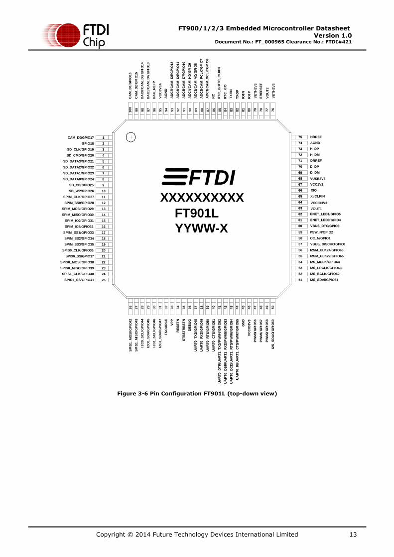
Figure 3-6 Pin Configuration FT901L (top-down view)
Copyright © 2014 Future Technology Devices International Limited 14
FT900/1/2/3 Embedded Microcontroller Datasheet Version 1.0
Document No.: FT_000965 Clearance No.: FTDI#421
CA
N0_
RX
D/C
AM
_D
1/G
PIO
16
CA
N0_
TX
D/C
AM
_D
2/G
PIO
15
DA
C0/C
AM
_D
3/G
PIO
14
DA
C1/C
AM
_D
4/G
PIO
13
DA
C_
RE
FP
AG
ND
AD
C7/C
AM
_D
5/G
PIO
12
NC
NC
NC
NC
NC
NC
RT
C_
XIO
RT
C_
XI/
RT
C_
CL
KIN
NC
AD
C1/C
AM
_X
CL
K/G
PIO
6
AD
C2/C
AM
_P
CL
K/G
PIO
7
AD
C3/C
AM
_V
D/G
PIO
8
AD
C4/C
AM
_H
D/G
PIO
9
AD
C5/C
AM
_D
7/G
PIO
10
AD
C6/C
AM
_D
6/G
PIO
11
10
0
85
86
87
88
89
90
91
92
93
94
95
96
97
98
99
76
77
78
79
80
81
82
83
84
36
35
34
33
32
31
30
29
28
27
26
48
47
46
45
44
43
42
41
40
39
38
37
49
50
SP
IS1_
MO
SI/
GP
IO4
2
SP
IS1
_M
ISO
/GP
IO4
3
I2C
0_
SC
L/G
PIO
44
I2C
0_
SD
A/G
PIO
45
I2C
1_
SC
L/G
PIO
46
I2C
1_
SD
A/G
PIO
47
FS
OU
RC
E
VP
P
RE
SE
TN
ST
ES
TR
ES
TN
DE
BU
G
UA
RT
0_
TX
D/G
PIO
48
UA
RT
0_
RX
D/G
PIO
49
UA
RT
0_
RT
S/G
PIO
50
UA
RT
0_
CT
S/G
PIO
51
UA
RT
0_
DT
R/U
AR
T1_
TX
D/P
WM
4/G
PIO
52
UA
RT
0_
DS
R/U
AR
T1_
RX
D/P
WM
5/G
PIO
53
UA
RT
0_
DC
D/U
AR
T1
_R
TS
/PW
M6/G
PIO
54
UA
RT
0_
RI/
UA
RT
1_
CT
S/P
WM
7/G
PIO
55
GN
D
PW
M0/G
PIO
56
PW
M1/G
PIO
57
PW
M2/G
PIO
58
I2S
_S
DA
O/G
PIO
60
2
3
4
5
6
7
8
9
10
11
12
13
14
15
16
1
24
25
17
18
19
20
21
22
23
SPIS1_SS/GPIO41
SPIS1_CLK/GPIO40
SPIS0_MISO/GPIO39
SPIS0_MOSI/GPIO38
SPIS0_SS/GPIO37
SPIS0_CLK/GPIO36
SPIM_SS3/GPIO35
SPIM_SS2/GPIO34
SPIM_SS1/GPIO33
SPIM_IO3/GPIO32
SPIM_IO2/GPIO31
SPIM_MISO/GPIO30
SPIM_MOSI/GPIO29
SPIM_SS0/GPIO28
SPIM_CLK/GPIO27
SD_WP/GPIO26
SD_CD/GPIO25
SD_DATA0/GPIO24
SD_DATA1/GPIO23
SD_DATA2/GPIO22
SD_DATA3/GPIO21
SD_CMD/GPIO20
SD_CLK/GPIO19
CAN1_TXD/CAM_D0/GPIO17
CAN1_RXD/GPIO18
HRREF
AGND
H_DP
H_DM
DRREF
D_DP
D_DM
VCC1V2
XIO
XI/CLKIN
GPIO5
GPIO4
VBUS_DTC/GPIO3
PSW_N/GPIO2
OC_N/GPIO1
VBUS_ DISCHG/ GPIO0
I2SM_CLK24/GPIO66
I2SM_CLK22/GPIO65
I2S_MCLK/GPIO64
I2S_LRCLK/GPIO63
I2S_BCLK/GPIO62
I2S_SDAI/GPIO61
60
61
62
63
64
65
66
67
68
69
70
71
72
73
74
75
51
52
53
54
55
56
57
58
59
FTDIXXXXXXXXXX
FT902L
YYWW-X
NC
NC
VC
CIO
3V
3
VCCIO3V3
VOUT1
VUSB3V3
VC
C3
V3
A
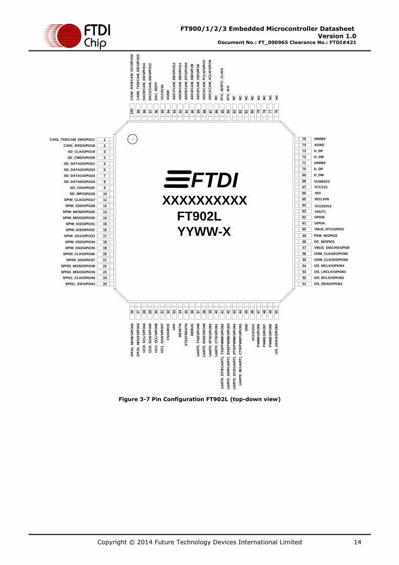
Figure 3-7 Pin Configuration FT902L (top-down view)
Copyright © 2014 Future Technology Devices International Limited 15
FT900/1/2/3 Embedded Microcontroller Datasheet Version 1.0
Document No.: FT_000965 Clearance No.: FTDI#421
CA
M_
D1/G
PIO
16
CA
M_
D2/G
PIO
15
DA
C0/C
AM
_D
3/G
PIO
14
DA
C1/C
AM
_D
4/G
PIO
13
DA
C_
RE
FP
AG
ND
AD
C7/C
AM
_D
5/G
PIO
12
NC
NC
NC
NC
NC
NC
RT
C_
XIO
RT
C_
XI/
RT
C_
CL
KIN
NC
AD
C1/C
AM
_X
CL
K/G
PIO
6
AD
C2/C
AM
_P
CL
K/G
PIO
7
AD
C3/C
AM
_V
D/G
PIO
8
AD
C4/C
AM
_H
D/G
PIO
9
AD
C5/C
AM
_D
7/G
PIO
10
AD
C6/C
AM
_D
6/G
PIO
11
10
0
85
86
87
88
89
90
91
92
93
94
95
96
97
98
99
76
77
78
79
80
81
82
83
84
36
35
34
33
32
31
30
29
28
27
26
48
47
46
45
44
43
42
41
40
39
38
37
49
50
SP
IS1_
MO
SI/
GP
IO4
2
SP
IS1
_M
ISO
/GP
IO4
3
I2C
0_
SC
L/G
PIO
44
I2C
0_
SD
A/G
PIO
45
I2C
1_
SC
L/G
PIO
46
I2C
1_
SD
A/G
PIO
47
FS
OU
RC
E
VP
P
RE
SE
TN
ST
ES
TR
ES
TN
DE
BU
G
UA
RT
0_
TX
D/G
PIO
48
UA
RT
0_
RX
D/G
PIO
49
UA
RT
0_
RT
S/G
PIO
50
UA
RT
0_
CT
S/G
PIO
51
UA
RT
0_
DT
R/U
AR
T1_
TX
D/P
WM
4/G
PIO
52
UA
RT
0_
DS
R/U
AR
T1_
RX
D/P
WM
5/G
PIO
53
UA
RT
0_
DC
D/U
AR
T1
_R
TS
/PW
M6/G
PIO
54
UA
RT
0_
RI/
UA
RT
1_
CT
S/P
WM
7/G
PIO
55
GN
D
PW
M0/G
PIO
56
PW
M1/G
PIO
57
PW
M2/G
PIO
58
I2S
_S
DA
O/G
PIO
60
2
3
4
5
6
7
8
9
10
11
12
13
14
15
16
1
24
25
17
18
19
20
21
22
23
SPIS1_SS/GPIO41
SPIS1_CLK/GPIO40
SPIS0_MISO/GPIO39
SPIS0_MOSI/GPIO38
SPIS0_SS/GPIO37
SPIS0_CLK/GPIO36
SPIM_SS3/GPIO35
SPIM_SS2/GPIO34
SPIM_SS1/GPIO33
SPIM_IO3/GPIO32
SPIM_IO2/GPIO31
SPIM_MISO/GPIO30
SPIM_MOSI/GPIO29
SPIM_SS0/GPIO28
SPIM_CLK/GPIO27
SD_WP/GPIO26
SD_CD/GPIO25
SD_DATA0/GPIO24
SD_DATA1/GPIO23
SD_DATA2/GPIO22
SD_DATA3/GPIO21
SD_CMD/GPIO20
SD_CLK/GPIO19
CAM_D0/GPIO17
GPIO18
HRREF
AGND
H_DP
H_DM
DRREF
D_DP
D_DM
VCC1V2
XIO
XI/CLKIN
GPIO5
GPIO4
VBUS_DTC/GPIO3
PSW_N/GPIO2
OC_N/GPIO1
VBUS_ DISCHG/ GPIO0
I2SM_CLK24/GPIO66
I2SM_CLK22/GPIO65
I2S_MCLK/GPIO64
I2S_LRCLK/GPIO63
I2S_BCLK/GPIO62
I2S_SDAI/GPIO61
60
61
62
63
64
65
66
67
68
69
70
71
72
73
74
75
51
52
53
54
55
56
57
58
59
FTDIXXXXXXXXXX
FT903L
YYWW-X
NC
NC
VC
CIO
3V
3
VCCIO3V3
VUSB3V3
VOUT1
VC
C3
V3
A
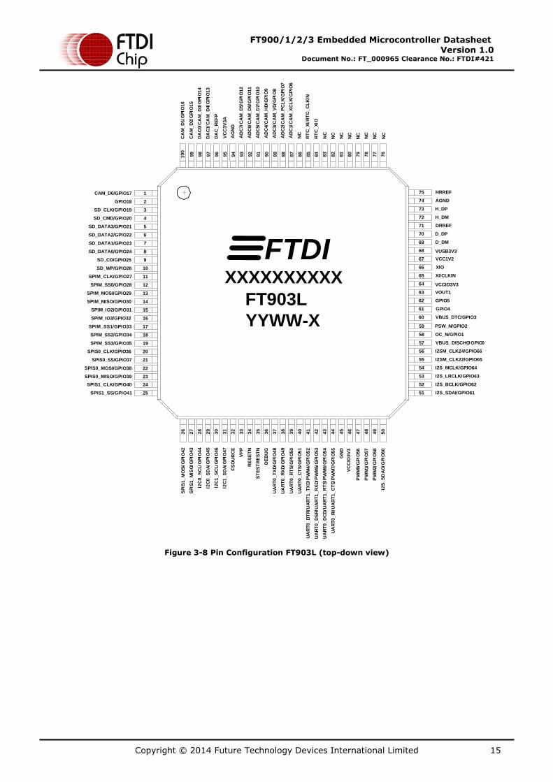
Figure 3-8 Pin Configuration FT903L (top-down view)
Copyright © 2014 Future Technology Devices International Limited 16
FT900/1/2/3 Embedded Microcontroller Datasheet Version 1.0
Document No.: FT_000965 Clearance No.: FTDI#421
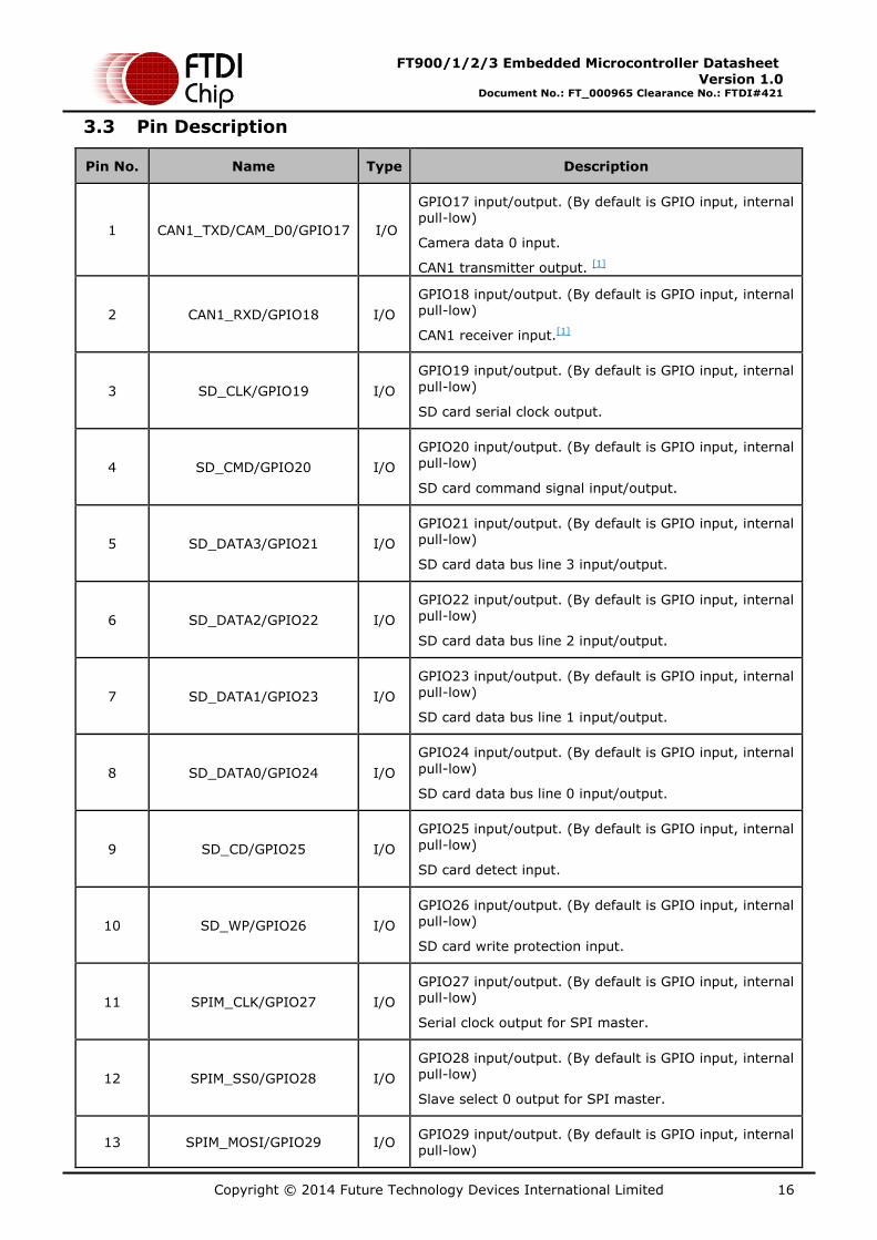
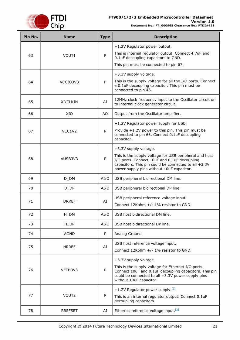
3.3 Pin Description
Pin No. Name Type Description
1 CAN1_TXD/CAM_D0/GPIO17 I/O
GPIO17 input/output. (By default is GPIO input, internal pull-low)
Camera data 0 input.
CAN1 transmitter output. [1]
2 CAN1_RXD/GPIO18 I/O
GPIO18 input/output. (By default is GPIO input, internal pull-low)
CAN1 receiver input.[1]
3 SD_CLK/GPIO19 I/O
GPIO19 input/output. (By default is GPIO input, internal
pull-low)
SD card serial clock output.
4 SD_CMD/GPIO20 I/O
GPIO20 input/output. (By default is GPIO input, internal pull-low)
SD card command signal input/output.
5 SD_DATA3/GPIO21 I/O
GPIO21 input/output. (By default is GPIO input, internal pull-low)
SD card data bus line 3 input/output.
6 SD_DATA2/GPIO22 I/O
GPIO22 input/output. (By default is GPIO input, internal pull-low)
SD card data bus line 2 input/output.
7 SD_DATA1/GPIO23 I/O
GPIO23 input/output. (By default is GPIO input, internal
pull-low)
SD card data bus line 1 input/output.
8 SD_DATA0/GPIO24 I/O
GPIO24 input/output. (By default is GPIO input, internal
pull-low)
SD card data bus line 0 input/output.
9 SD_CD/GPIO25 I/O
GPIO25 input/output. (By default is GPIO input, internal pull-low)
SD card detect input.
10 SD_WP/GPIO26 I/O
GPIO26 input/output. (By default is GPIO input, internal pull-low)
SD card write protection input.
11 SPIM_CLK/GPIO27 I/O
GPIO27 input/output. (By default is GPIO input, internal pull-low)
Serial clock output for SPI master.
12 SPIM_SS0/GPIO28 I/O
GPIO28 input/output. (By default is GPIO input, internal pull-low)
Slave select 0 output for SPI master.
13 SPIM_MOSI/GPIO29 I/O GPIO29 input/output. (By default is GPIO input, internal pull-low)
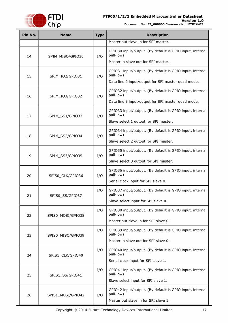
Copyright © 2014 Future Technology Devices International Limited 17
FT900/1/2/3 Embedded Microcontroller Datasheet Version 1.0
Document No.: FT_000965 Clearance No.: FTDI#421
Pin No. Name Type Description
Master out slave in for SPI master.
14 SPIM_MISO/GPIO30 I/O
GPIO30 input/output. (By default is GPIO input, internal pull-low)
Master in slave out for SPI master.
15 SPIM_IO2/GPIO31 I/O
GPIO31 input/output. (By default is GPIO input, internal pull-low)
Data line 2 input/output for SPI master quad mode.
16 SPIM_IO3/GPIO32 I/O
GPIO32 input/output. (By default is GPIO input, internal pull-low)
Data line 3 input/output for SPI master quad mode.
17 SPIM_SS1/GPIO33 I/O
GPIO33 input/output. (By default is GPIO input, internal pull-low)
Slave select 1 output for SPI master.
18 SPIM_SS2/GPIO34 I/O
GPIO34 input/output. (By default is GPIO input, internal pull-low)
Slave select 2 output for SPI master.
19 SPIM_SS3/GPIO35 I/O
GPIO35 input/output. (By default is GPIO input, internal pull-low)
Slave select 3 output for SPI master.
20 SPIS0_CLK/GPIO36 I/O
GPIO36 input/output. (By default is GPIO input, internal pull-low)
Serial clock input for SPI slave 0.
21 SPIS0_SS/GPIO37
I/O GPIO37 input/output. (By default is GPIO input, internal
pull-low)
Slave select input for SPI slave 0.
22 SPIS0_MOSI/GPIO38
I/O GPIO38 input/output. (By default is GPIO input, internal pull-low)
Master out slave in for SPI slave 0.
23 SPIS0_MISO/GPIO39
I/O GPIO39 input/output. (By default is GPIO input, internal pull-low)
Master in slave out for SPI slave 0.
24 SPIS1_CLK/GPIO40
I/O GPIO40 input/output. (By default is GPIO input, internal
pull-low)
Serial clock input for SPI slave 1.
25 SPIS1_SS/GPIO41
I/O GPIO41 input/output. (By default is GPIO input, internal pull-low)
Slave select input for SPI slave 1.
26 SPIS1_MOSI/GPIO42 I/O
GPIO42 input/output. (By default is GPIO input, internal
pull-low)
Master out slave in for SPI slave 1.
Copyright © 2014 Future Technology Devices International Limited 18
FT900/1/2/3 Embedded Microcontroller Datasheet Version 1.0
Document No.: FT_000965 Clearance No.: FTDI#421
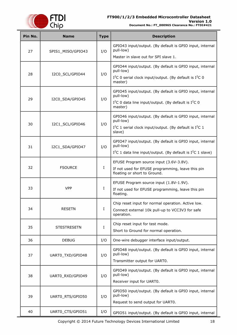
Pin No. Name Type Description
27 SPIS1_MISO/GPIO43 I/O
GPIO43 input/output. (By default is GPIO input, internal
pull-low)
Master in slave out for SPI slave 1.
28 I2C0_SCL/GPIO44 I/O
GPIO44 input/output. (By default is GPIO input, internal pull-low)
I2C 0 serial clock input/output. (By default is I2C 0 master)
29 I2C0_SDA/GPIO45 I/O
GPIO45 input/output. (By default is GPIO input, internal pull-low)
I2C 0 data line input/output. (By default is I2C 0
master)
30 I2C1_SCL/GPIO46 I/O
GPIO46 input/output. (By default is GPIO input, internal pull-low)
I2C 1 serial clock input/output. (By default is I2C 1
slave)
31 I2C1_SDA/GPIO47 I/O
GPIO47 input/output. (By default is GPIO input, internal pull-low)
I2C 1 data line input/output. (By default is I2C 1 slave)
32 FSOURCE I
EFUSE Program source input (3.6V-3.8V).
If not used for EFUSE programming, leave this pin floating or short to Ground.
33 VPP I
EFUSE Program source input (1.8V-1.9V).
If not used for EFUSE programming, leave this pin floating.
34 RESETN I
Chip reset input for normal operation. Active low.
Connect external 10k pull-up to VCC3V3 for safe operation.
35 STESTRESETN I Chip reset input for test mode.
Short to Ground for normal operation.
36 DEBUG I/O One-wire debugger interface input/output.
37 UART0_TXD/GPIO48 I/O
GPIO48 input/output. (By default is GPIO input, internal pull-low)
Transmitter output for UART0.
38 UART0_RXD/GPIO49 I/O
GPIO49 input/output. (By default is GPIO input, internal pull-low)
Receiver input for UART0.
39 UART0_RTS/GPIO50 I/O
GPIO50 input/output. (By default is GPIO input, internal pull-low)
Request to send output for UART0.
40 UART0_CTS/GPIO51 I/O GPIO51 input/output. (By default is GPIO input, internal
Copyright © 2014 Future Technology Devices International Limited 19
FT900/1/2/3 Embedded Microcontroller Datasheet Version 1.0
Document No.: FT_000965 Clearance No.: FTDI#421
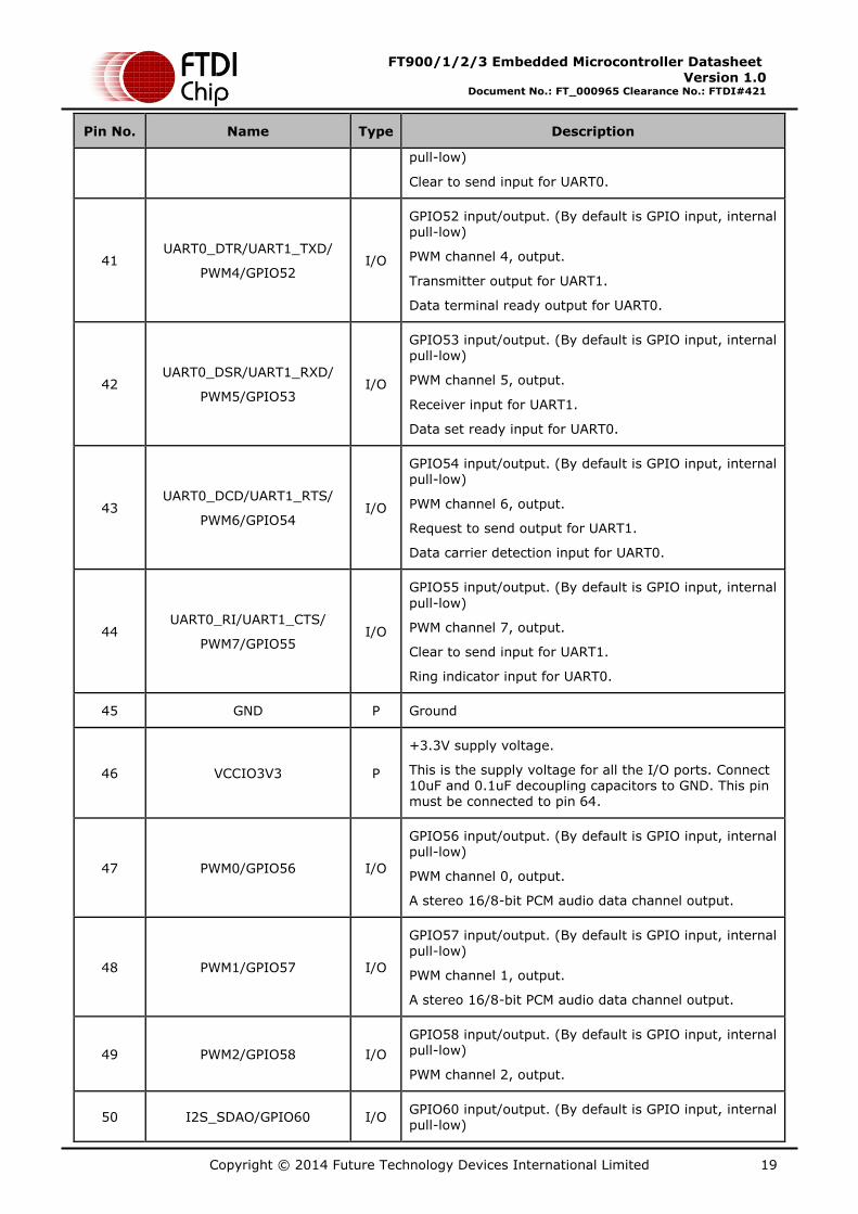
Pin No. Name Type Description
pull-low)
Clear to send input for UART0.
41 UART0_DTR/UART1_TXD/
PWM4/GPIO52 I/O
GPIO52 input/output. (By default is GPIO input, internal pull-low)
PWM channel 4, output.
Transmitter output for UART1.
Data terminal ready output for UART0.
42 UART0_DSR/UART1_RXD/
PWM5/GPIO53 I/O
GPIO53 input/output. (By default is GPIO input, internal pull-low)
PWM channel 5, output.
Receiver input for UART1.
Data set ready input for UART0.
43 UART0_DCD/UART1_RTS/
PWM6/GPIO54 I/O
GPIO54 input/output. (By default is GPIO input, internal pull-low)
PWM channel 6, output.
Request to send output for UART1.
Data carrier detection input for UART0.
44 UART0_RI/UART1_CTS/
PWM7/GPIO55 I/O
GPIO55 input/output. (By default is GPIO input, internal
pull-low)
PWM channel 7, output.
Clear to send input for UART1.
Ring indicator input for UART0.
45 GND P Ground
46 VCCIO3V3 P
+3.3V supply voltage.
This is the supply voltage for all the I/O ports. Connect 10uF and 0.1uF decoupling capacitors to GND. This pin must be connected to pin 64.
47 PWM0/GPIO56 I/O
GPIO56 input/output. (By default is GPIO input, internal pull-low)
PWM channel 0, output.
A stereo 16/8-bit PCM audio data channel output.
48 PWM1/GPIO57 I/O
GPIO57 input/output. (By default is GPIO input, internal
pull-low)
PWM channel 1, output.
A stereo 16/8-bit PCM audio data channel output.
49 PWM2/GPIO58 I/O
GPIO58 input/output. (By default is GPIO input, internal pull-low)
PWM channel 2, output.
50 I2S_SDAO/GPIO60 I/O GPIO60 input/output. (By default is GPIO input, internal pull-low)
Copyright © 2014 Future Technology Devices International Limited 20
FT900/1/2/3 Embedded Microcontroller Datasheet Version 1.0
Document No.: FT_000965 Clearance No.: FTDI#421
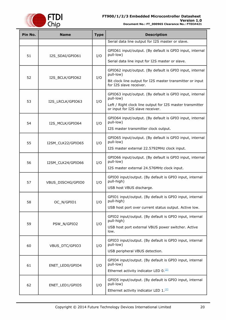
Pin No. Name Type Description
Serial data line output for I2S master or slave.
51 I2S_SDAI/GPIO61 I/O
GPIO61 input/output. (By default is GPIO input, internal pull-low)
Serial data line input for I2S master or slave.
52 I2S_BCLK/GPIO62 I/O
GPIO62 input/output. (By default is GPIO input, internal pull-low)
Bit clock line output for I2S master transmitter or input for I2S slave receiver.
53 I2S_LRCLK/GPIO63 I/O
GPIO63 input/output. (By default is GPIO input, internal pull-low)
Left / Right clock line output for I2S master transmitter
or input for I2S slave receiver.
54 I2S_MCLK/GPIO64 I/O
GPIO64 input/output. (By default is GPIO input, internal pull-low)
I2S master transmitter clock output.
55 I2SM_CLK22/GPIO65 I/O
GPIO65 input/output. (By default is GPIO input, internal
pull-low)
I2S master external 22.5792MHz clock input.
56 I2SM_CLK24/GPIO66 I/O
GPIO66 input/output. (By default is GPIO input, internal pull-low)
I2S master external 24.576MHz clock input.
57 VBUS_DISCHG/GPIO0 I/O
GPIO0 input/output. (By default is GPIO input, internal
pull-high)
USB host VBUS discharge.
58 OC_N/GPIO1 I/O
GPIO1 input/output. (By default is GPIO input, internal pull-high)
USB host port over current status output. Active low.
59 PSW_N/GPIO2 I/O
GPIO2 input/output. (By default is GPIO input, internal pull-high)
USB host port external VBUS power switcher. Active low.
60 VBUS_DTC/GPIO3 I/O
GPIO3 input/output. (By default is GPIO input, internal
pull-low)
USB peripheral VBUS detection.
61 ENET_LED0/GPIO4 I/O
GPIO4 input/output. (By default is GPIO input, internal pull-low)
Ethernet activity indicator LED 0.[2]
62 ENET_LED1/GPIO5 I/O
GPIO5 input/output. (By default is GPIO input, internal pull-low)
Ethernet activity indicator LED 1.[2]
Copyright © 2014 Future Technology Devices International Limited 21
FT900/1/2/3 Embedded Microcontroller Datasheet Version 1.0
Document No.: FT_000965 Clearance No.: FTDI#421
Pin No. Name Type Description
63 VOUT1 P
+1.2V Regulator power output.
This is internal regulator output. Connect 4.7uF and 0.1uF decoupling capacitors to GND.
This pin must be connected to pin 67.
64 VCCIO3V3 P
+3.3V supply voltage.
This is the supply voltage for all the I/O ports. Connect a 0.1uF decoupling capacitor. This pin must be connected to pin 46.
65 XI/CLKIN AI 12MHz clock frequency input to the Oscillator circuit or to internal clock generator circuit.
66 XIO AO Output from the Oscillator amplifier.
67 VCC1V2 P
+1.2V Regulator power supply for USB.
Provide +1.2V power to this pin. This pin must be connected to pin 63. Connect 0.1uF decoupling capacitor.
68 VUSB3V3 P
+3.3V supply voltage.
This is the supply voltage for USB peripheral and host I/O ports. Connect 10uF and 0.1uF decoupling capacitors. This pin could be connected to all +3.3V power supply pins without 10uF capacitor.
69 D_DM AI/O USB peripheral bidirectional DM line.
70 D_DP AI/O USB peripheral bidirectional DP line.
71 DRREF AI USB peripheral reference voltage input.
Connect 12Kohm +/- 1% resistor to GND.
72 H_DM AI/O USB host bidirectional DM line.
73 H_DP AI/O USB host bidirectional DP line.
74 AGND P Analog Ground
75 HRREF AI USB host reference voltage input.
Connect 12Kohm +/- 1% resistor to GND.
76 VETH3V3 P
+3.3V supply voltage.
This is the supply voltage for Ethernet I/O ports. Connect 10uF and 0.1uF decoupling capacitors. This pin
could be connected to all +3.3V power supply pins without 10uF capacitor.
77 VOUT2 P
+1.2V Regulator power supply.[2]
This is an internal regulator output. Connect 0.1uF
decoupling capacitors.
78 RREFSET AI Ethernet reference voltage input.[2]
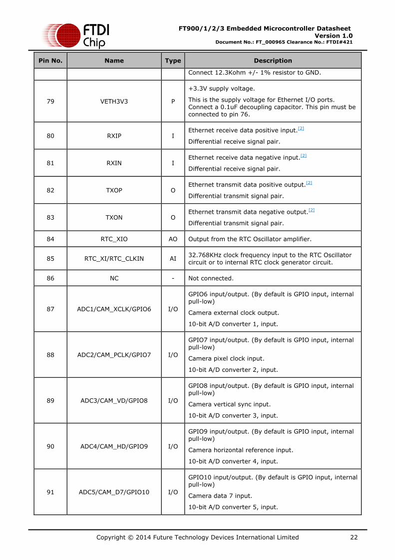
Copyright © 2014 Future Technology Devices International Limited 22
FT900/1/2/3 Embedded Microcontroller Datasheet Version 1.0
Document No.: FT_000965 Clearance No.: FTDI#421
Pin No. Name Type Description
Connect 12.3Kohm +/- 1% resistor to GND.
79 VETH3V3 P
+3.3V supply voltage.
This is the supply voltage for Ethernet I/O ports. Connect a 0.1uF decoupling capacitor. This pin must be connected to pin 76.
80 RXIP I Ethernet receive data positive input.[2]
Differential receive signal pair.
81 RXIN I Ethernet receive data negative input.[2]
Differential receive signal pair.
82 TXOP O Ethernet transmit data positive output.[2]
Differential transmit signal pair.
83 TXON O Ethernet transmit data negative output.[2]
Differential transmit signal pair.
84 RTC_XIO AO Output from the RTC Oscillator amplifier.
85 RTC_XI/RTC_CLKIN AI 32.768KHz clock frequency input to the RTC Oscillator circuit or to internal RTC clock generator circuit.
86 NC - Not connected.
87 ADC1/CAM_XCLK/GPIO6 I/O
GPIO6 input/output. (By default is GPIO input, internal pull-low)
Camera external clock output.
10-bit A/D converter 1, input.
88 ADC2/CAM_PCLK/GPIO7 I/O
GPIO7 input/output. (By default is GPIO input, internal pull-low)
Camera pixel clock input.
10-bit A/D converter 2, input.
89 ADC3/CAM_VD/GPIO8 I/O
GPIO8 input/output. (By default is GPIO input, internal pull-low)
Camera vertical sync input.
10-bit A/D converter 3, input.
90 ADC4/CAM_HD/GPIO9 I/O
GPIO9 input/output. (By default is GPIO input, internal
pull-low)
Camera horizontal reference input.
10-bit A/D converter 4, input.
91 ADC5/CAM_D7/GPIO10 I/O
GPIO10 input/output. (By default is GPIO input, internal pull-low)
Camera data 7 input.
10-bit A/D converter 5, input.
Copyright © 2014 Future Technology Devices International Limited 23
FT900/1/2/3 Embedded Microcontroller Datasheet Version 1.0
Document No.: FT_000965 Clearance No.: FTDI#421
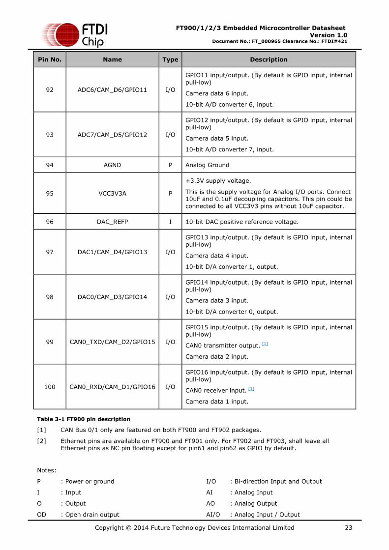
Pin No. Name Type Description
92 ADC6/CAM_D6/GPIO11 I/O
GPIO11 input/output. (By default is GPIO input, internal
pull-low)
Camera data 6 input.
10-bit A/D converter 6, input.
93 ADC7/CAM_D5/GPIO12 I/O
GPIO12 input/output. (By default is GPIO input, internal
pull-low)
Camera data 5 input.
10-bit A/D converter 7, input.
94 AGND P Analog Ground
95 VCC3V3A P
+3.3V supply voltage.
This is the supply voltage for Analog I/O ports. Connect 10uF and 0.1uF decoupling capacitors. This pin could be connected to all VCC3V3 pins without 10uF capacitor.
96 DAC_REFP I 10-bit DAC positive reference voltage.
97 DAC1/CAM_D4/GPIO13 I/O
GPIO13 input/output. (By default is GPIO input, internal pull-low)
Camera data 4 input.
10-bit D/A converter 1, output.
98 DAC0/CAM_D3/GPIO14 I/O
GPIO14 input/output. (By default is GPIO input, internal pull-low)
Camera data 3 input.
10-bit D/A converter 0, output.
99 CAN0_TXD/CAM_D2/GPIO15 I/O
GPIO15 input/output. (By default is GPIO input, internal pull-low)
CAN0 transmitter output. [1]
Camera data 2 input.
100 CAN0_RXD/CAM_D1/GPIO16 I/O
GPIO16 input/output. (By default is GPIO input, internal pull-low)
CAN0 receiver input. [1]
Camera data 1 input.
Table 3-1 FT900 pin description
[1] CAN Bus 0/1 only are featured on both FT900 and FT902 packages.
[2] Ethernet pins are available on FT900 and FT901 only. For FT902 and FT903, shall leave all Ethernet pins as NC pin floating except for pin61 and pin62 as GPIO by default.
Notes:
P : Power or ground
I : Input
O : Output
OD : Open drain output
I/O : Bi-direction Input and Output
AI : Analog Input
AO : Analog Output
AI/O : Analog Input / Output
Copyright © 2014 Future Technology Devices International Limited 24
FT900/1/2/3 Embedded Microcontroller Datasheet Version 1.0
Document No.: FT_000965 Clearance No.: FTDI#421
4 Function Description
4.1 Architectural Overview
The FT900 series embedded microcontroller includes a high performance 32-bit FT32 RISC
core processor and 256kB hi-speed Flash memory for software program download with One-
Wire debugger interface. The core processor uses a 32-bit I/O system bus to connect to all of
the peripherals.
USB2.0 host controller
USB2.0 peripheral controller
10/100Mbps Ethernet controller (FT900 and FT901 only)
Two CAN bus interfaces (FT900 and FT902 only)
Real Time Clock
One-Wire debugger interface
One SPI master interface and two SPI slave interfaces
Two I2C bus interfaces
One I2S bus interface
UART interface
Four timers and a 32-bit watchdog timer
Camera parallel interface
SD host controller
PWM motor controller
10-bit DAC0/1 channel
10-bit ADC1-7 channel
General purpose I/O interface
The functions for each controller / interface are briefly described in the following subsections.
4.2 FT32 Core Processor
The FT32 core processor is running at frequencies of up to 100MHz. The processor contains the
CPU itself with control logic and its 256kB program memory and 64kB data memory. The
outside connections for the core processor are the memory-mapped I/O interface, the interrupt
interface, asynchronous reset and the system clock.
4.3 256kB Flash Memory
The internal 256kB Flash memory is used to store a boot loader or user application of the
FT900 series. It is a high performance and low power consumption memory that supports upto
80MHz serial clock. The system will perform memory copy from Flash memory to CPU program
memory automatically after system power on.
4.4 Boot Sequence
After the initial memory copy completes, the CPU jumps to program memory location zero.
This may be the start of the user application which is stored in advance in Flash memory, or a
boot loader only which allows program memory to perform modification via (e.g.) UART or
USB.
The option of a boot loader is a special purpose routine in the FT900 series embedded
microcontroller. It is small routine stored in the Flash memory. Typically the boot loader is 1-
4kbytes in size, and is loaded at the top of the available memory.
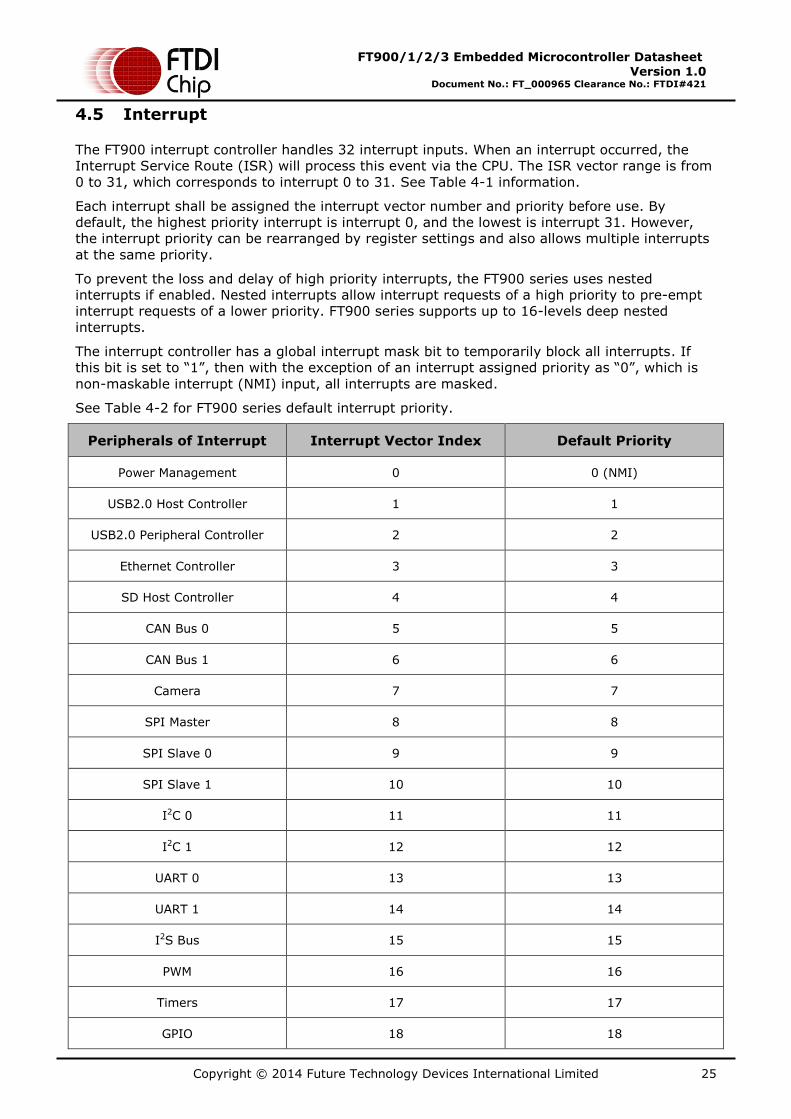
Copyright © 2014 Future Technology Devices International Limited 25
FT900/1/2/3 Embedded Microcontroller Datasheet Version 1.0
Document No.: FT_000965 Clearance No.: FTDI#421
4.5 Interrupt
The FT900 interrupt controller handles 32 interrupt inputs. When an interrupt occurred, the
Interrupt Service Route (ISR) will process this event via the CPU. The ISR vector range is from
0 to 31, which corresponds to interrupt 0 to 31. See Table 4-1 information.
Each interrupt shall be assigned the interrupt vector number and priority before use. By
default, the highest priority interrupt is interrupt 0, and the lowest is interrupt 31. However,
the interrupt priority can be rearranged by register settings and also allows multiple interrupts
at the same priority.
To prevent the loss and delay of high priority interrupts, the FT900 series uses nested
interrupts if enabled. Nested interrupts allow interrupt requests of a high priority to pre-empt
interrupt requests of a lower priority. FT900 series supports up to 16-levels deep nested
interrupts.
The interrupt controller has a global interrupt mask bit to temporarily block all interrupts. If
this bit is set to “1”, then with the exception of an interrupt assigned priority as “0”, which is
non-maskable interrupt (NMI) input, all interrupts are masked.
See Table 4-2 for FT900 series default interrupt priority.
Peripherals of Interrupt Interrupt Vector Index Default Priority
Power Management 0 0 (NMI)
USB2.0 Host Controller 1 1
USB2.0 Peripheral Controller 2 2
Ethernet Controller 3 3
SD Host Controller 4 4
CAN Bus 0 5 5
CAN Bus 1 6 6
Camera 7 7
SPI Master 8 8
SPI Slave 0 9 9
SPI Slave 1 10 10
I2C 0 11 11
I2C 1 12 12
UART 0 13 13
UART 1 14 14
I2S Bus 15 15
PWM 16 16
Timers 17 17
GPIO 18 18

Copyright © 2014 Future Technology Devices International Limited 26
FT900/1/2/3 Embedded Microcontroller Datasheet Version 1.0
Document No.: FT_000965 Clearance No.: FTDI#421
Peripherals of Interrupt Interrupt Vector Index Default Priority
RTC 19 19
ADC 20 20
DAC 21 21
Slow Clock Timer 22 22
UNUSED 23-31 23-31
Table 4-1 FT900 series default interrupt priority
4.6 Memory Mapping
A list of the I/O memory mapping for registers and memory in the FT900 series is given below
in table 4-2. Please refer to FT900 User Manual for detail description of registers.
Function Address Memory Range Comment
General setup registers 0x10000 0x100BF DW/W/B
Interrupt controller registers 0x100C0 0x100FF DW/W/B
USB2.0 host controller registers 0x10100 0x1017F DW/W/B
USB2.0 host controller RAM
memory
0x11000 0x12FFF DW/W/B
USB2.0 peripheral controller
registers
0x10180 0x1021F DW/W/B
Ethernet controller registers 0x10220 0x1023F DW/W/B (Uses DW to access
FIFO)
CAN BUS 0 registers 0x10240 0x1025F B
CAN BUS 1 registers 0x10260 0x1027F B
RTC registers 0x10280 0x1029F DW
SPI master registers 0x102A0 0x102BF DW
SPI slave 0 registers 0x102C0 0x102DF DW
SPI slave 1 registers 0x102E0 0x102FF DW
I2C master registers 0x10300 0x1030F B (I2C 0 and I2C 1 both can be configure as master or
slave)
I2C slave registers 0x10310 0x1031F
B (I2C 0 and I2C 1 both can
be configure as master or slave)
UART 0 register 0x10320 0x1032F B
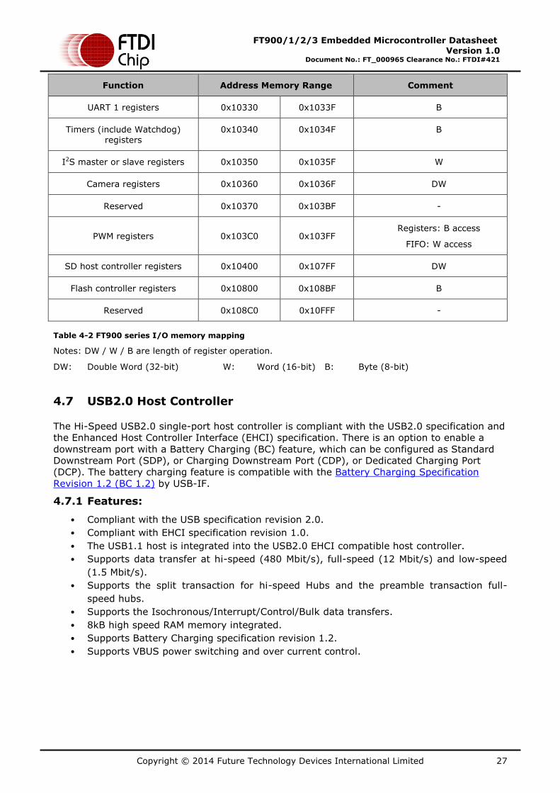
Copyright © 2014 Future Technology Devices International Limited 27
FT900/1/2/3 Embedded Microcontroller Datasheet Version 1.0
Document No.: FT_000965 Clearance No.: FTDI#421
Function Address Memory Range Comment
UART 1 registers 0x10330 0x1033F B
Timers (include Watchdog)
registers
0x10340 0x1034F B
I2S master or slave registers 0x10350 0x1035F W
Camera registers 0x10360 0x1036F DW
Reserved 0x10370 0x103BF -
PWM registers 0x103C0 0x103FF Registers: B access
FIFO: W access
SD host controller registers 0x10400 0x107FF DW
Flash controller registers 0x10800 0x108BF B
Reserved 0x108C0 0x10FFF -
Table 4-2 FT900 series I/O memory mapping
Notes: DW / W / B are length of register operation.
DW: Double Word (32-bit) W: Word (16-bit) B: Byte (8-bit)
4.7 USB2.0 Host Controller
The Hi-Speed USB2.0 single-port host controller is compliant with the USB2.0 specification and
the Enhanced Host Controller Interface (EHCI) specification. There is an option to enable a
downstream port with a Battery Charging (BC) feature, which can be configured as Standard
Downstream Port (SDP), or Charging Downstream Port (CDP), or Dedicated Charging Port
(DCP). The battery charging feature is compatible with the Battery Charging Specification
Revision 1.2 (BC 1.2) by USB-IF.
4.7.1 Features:
• Compliant with the USB specification revision 2.0.
• Compliant with EHCI specification revision 1.0.
• The USB1.1 host is integrated into the USB2.0 EHCI compatible host controller.
• Supports data transfer at hi-speed (480 Mbit/s), full-speed (12 Mbit/s) and low-speed
(1.5 Mbit/s).
• Supports the split transaction for hi-speed Hubs and the preamble transaction full-
speed hubs.
• Supports the Isochronous/Interrupt/Control/Bulk data transfers.
• 8kB high speed RAM memory integrated.
• Supports Battery Charging specification revision 1.2.
• Supports VBUS power switching and over current control.

Copyright © 2014 Future Technology Devices International Limited 28
FT900/1/2/3 Embedded Microcontroller Datasheet Version 1.0
Document No.: FT_000965 Clearance No.: FTDI#421
4.8 USB2.0 Peripheral Contoller
The USB 2.0 peripheral controller is fully compliant with the USB2.0 specification. There is also
an option to enable a battery charger detection (BCD) feature on the upstream port, which can
identify whether the connected downstream port supports SDP, CDP or DCP charging function.
Battery charge detection allows the USB device to determine if higher currents may be
available from the USB connection for rapid battery charging.
4.8.1 Features:
Supports data transfer at hi-speed (480 Mbit/s) and full-speed (12 Mbit/s).
Software configurable EP0 control endpoint size 8-64 bytes
Software configurable 7 IN/OUT endpoints.
EP1-EP7 has double buffering which contains 2kB IN and 2kB OUT buffers.
Supports the Isochronous/Interrupt/Control/Bulk data transfers.
Max endpoint packet sizes upon 1024 bytes.
Supports VBUS detection.
Supports suspend and resume power management functions.
Supports remote wakeup feature.
Supports Battery Charging specification revision 1.2.
4.9 Ethernet Controller
The Ethernet controller contains an on-chip 10/100BASE-TX Ethernet transceiver and Media
Access Control (MAC) designed to provide high performance of frame transmission and
reception. The Ethernet transceiver is compliant with 10/100BASE-TX Ethernet standards, such
as IEEE802.3/802.3u and ANSI X3.263-1995, and MAC protocol refers to an IEEE standard
802.3-2000.
4.9.1 Features:
10/100 Mbps data transfer.
Conforms to IEEE 802.3-2002 specification.
Supports full-duplex and half-duplex modes.
- Supports CSMA/CD protocol for half-duplex operation.
- Supports IEEE802.3x flow control for full-duplex operation.
Programmable MAC address.
CRC-32 algorithm calculates the FCS nibble at a time, automatic FCS generation and
checking, able to capture frames with CRC errors if required.
Promiscuous mode support.
Station Management (STA) entity included.
Supports double buffering for 2kB TX and 2kB RX memory.
Two LED indicators used by Ethernet multi-function.
4.10 CAN Bus Controller
The FT900 series contains two controllers, CAN bus 0 and CAN bus 1. Controller Area Network
(CAN) is a high performance communication protocol for serial data communication. It is
widely used in automotive and industrial applications. However this is expanding due to its
reliability and feasibility. CAN bus uses a multi-master bus scheme with one logic bus line and
equal nodes. The number of nodes is not limited by the protocol. Nodes do not have specific
addresses. Instead, message identifiers are used, indicating the message content and priority
of the message. FT900 CAN bus supports multicasting and broadcasting with an external CAN
transceiver.
Copyright © 2014 Future Technology Devices International Limited 29
FT900/1/2/3 Embedded Microcontroller Datasheet Version 1.0
Document No.: FT_000965 Clearance No.: FTDI#421
4.10.1 Features:
Conforms to protocol version 2.0 parts A and B.
Supports bit rates of up to 1 Mbit/s.
Supports standard (11-bit identifier) and extended (29-bit identifier) frames.
Support hardware message filtering with dual/single filters.
64 Bytes receiver and 16 Bytes transmitter FIFO.
No overload frames are generated.
Supports normal and listen-only modes.
Supports single shot transmission.
Supports an abort transmission feature.
Readable error counters and last error code capture supported.
4.11 Real Time Clock
The Real Time Clock (RTC) is a set of counters for measuring time when system power is on,
and the internal regulator will provide power to the RTC. It is clocked by a 32.768 kHz
oscillator.
4.11.1 Features:
No need external battery power supply.
Alarm interrupt can be generated for a specific data/time setting.
Hardware reset does not interrupt the RTC counter.
4.12 One-Wire Debugger Interface
The Debugger interface provides the capability, over a One-Wire half duplex serial link, to
access memory mapped address space, such as the FT900 Flash memory, program memory,
data memory and I/O memory. However, there is no transfer capability from any of the
internal memory to the debugger interface.
4.12.1 Features:
Single wire half duplex link that has one Start, eight Data and one Stop bits at a 1M
bit/s rate.
Supports debugger command read / write operation with variable data transfer.
Supports CHIP ID read out.
Supports checksum check by Flash memory operation.
Supports CPU software debugging to execute Run, Stop, Step, Halt, Set software
breakpoint, etc. operations.
Use semaphore flag to control resource allocated by CPU or Debugger.
4.13 SPI Interface
The FT900 series contains an SPI master and SPI0, SPI1 slave controllers. SPI is a full duplex
serial interface designed to handle multiple masters and slaves connected to a given bus.
4.13.1 Features:
Maximum SPI data bit rate 25MHz in master and slave modes.
Full duplex synchronous serial data transfer.
Compliant with SPI specification, support four transfer formats.
SPI master supports Single, Dual and Quad SPI transfer.
SPI0, SPI1 slave support Single transfer only.
Copyright © 2014 Future Technology Devices International Limited 30
FT900/1/2/3 Embedded Microcontroller Datasheet Version 1.0
Document No.: FT_000965 Clearance No.: FTDI#421
Support SPI mode and FIFO mode operations.
Multi-master system supported.
Support bus error detection.
SPI master can address up to 4 SPI slave devices.
Support 64 Bytes receiver and 64 Bytes transmitter FIFO respectively.
4.14 I2C Interface
The FT900 series supports an I2C bus controller which is a bidirectional, two wires (a Serial
Clock line (SCL) and a Serial Data line (SDA)) interface. The interface can be programed to
operate with arbitration and clock synchronization allowing it to operate in multi-master
systems. I2C0 and I2C1 support transmission speed up to 3.4Mb/s.
4.14.1 Features:
Conform to v2.1 and v3.0 of the I2C specification.
Support flexible transmission speed modes.
- Standard (up to 100 kb/s)
- Fast (up to 400 kb/s)
- Fast-plus (up to 1 Mb/s)
- High-speed (up to 3.4 Mb/s)
I2C0 and I2C1 can be configured for Master or Slave mode.
Perform arbitration and clock synchronization.
Multi-master systems supported.
Support both 7-bit and 10-bit addressing modes on the I2C bus.
Support clock stretching.
4.15 UART Interface
The FT900 series contains two UART controllers with standard transmit and receive data lines.
UART0 provides a full modem control handshake interface and support for 9-bit data, allowing
automatic address detection while 9-bit data mode is enabled.
UART1 is a simplified programmable serial interface with CTS and RTS flow control logic. The
signals are multiplexed with UART0 and can only be used if UART0 is used in simple mode
(CTS/RTS only).
4.15.1 Features:
Maximum UART data bit rate of 8 Mbit/s.
Support UART mode and FIFO mode operation.
128 Bytes buffering both Receive and Transmit FIFOs used.
Software compatible with 16450, 16550, 16750 and 16950 industry standard.
Modem control function (CTS, RTS, DSR, DTR, RI, and DCD) support for UART0.
Programmable automatic out-of- band flow control logic through Auto-RTS and Auto-
CTS.
Programmable automatic flow control logic using DTR and DSR.
Programmable automatic in-band flow control logic using XON/XOFF characters.
Support external RS-485 buffer enable.
Fully programmable serial interface characteristics:
- 5-, 6-, 7-, 8-, or 9-bit data characters
- Even, Odd, or No-parity bit generation and detection
- 1-, 1.5- or 2-stop bit generation
- Baud generation
- Detection of bad data in Receive FIFO

Copyright © 2014 Future Technology Devices International Limited 31
FT900/1/2/3 Embedded Microcontroller Datasheet Version 1.0
Document No.: FT_000965 Clearance No.: FTDI#421
Support Transmitter and Receiver disable capability.
4.16 Timers and Watchdog Timer
The FT900 series has four 16-bit user timers with pre-scaling and a 32-bit watchdog feature.
The watchdog timer is controlled from the main clock. The watchdog can be initialized with a
5-bit register. The value of this register points to a bit of the 32-bit counter which will be set
by the application firmware. As the timer decrements, an interrupt occurs when the timer rolls
over. Once started and initialized the watchdog can’t be stopped. It can only be cleared by
writing into a register.
The four user timers can be controlled from the main clock or a common 16-bit pre-scaler,
which can be selected by each timer individually. These timers can be started, stopped and
cleared / initialized. The current value of all timers can be read from registers. All timers can
count up / down and signal an interrupt when the timer rolls over. The timers can also be
configured to be one-shot or in continuous mode.
4.16.1 Features:
Four user timers with pre-scaler.
Supports 16-bit pre-scaler with system clock reference.
Supports individual timer interrupt generated.
Supports one-shot and continuous count for timer.
Supports 32-bit counter watchdog.
Supports watchdog interrupt generated.
4.17 I2S Interface
The FT900 I2S interface supports both Master and Slave modes. The formats supported are
I2S, Left Justified and Right Justified.
In Master mode, two clock sources are to be provided externally. One is 24.576MHz and the
other is 22.5792MHz. The LRCLK, BCLK and MCLK as output signals will be generated by the
Master based on sampling rate and data bit length.
In Slave mode, the LRCLK and BCLK are input signals to the FT900. The MCLK source is not
used in this case. The application can configure the two clock source pins (I2SM_CLK22,
I2SM_CLK24) to GPIO operation.
4.17.1 Features:
Configure I2S interface as master or slave.
Support I2S, Left Justified and Right Justified format.
Support different sample rates: 11.025KHz, 22.05KHz, 44.1KHz, 16KHz, 32KHz, 48KHz,
96KHz and 192KHz.
Support different audio data bit length: 16 bits, 20 bits, 24 bits and 32 bits.
2kB FIFO for I2S receiver and 2kB FIFO for transfer audio data.
Support FIFO flow control.
Support master clock sources: 24.576MHz and 22.5792MHz.
4.18 Camera Parallel Interface (Data Capture)
The Camera Parallel Interface (CPI) implements an 8-bit parallel link from an image sensor to
FT900. The interface will provide a clock to the external camera module at a Max 25MHz.
Camera control signals are VSYNC, HREF and PCLK. The VSYNC signal determines when a new
frame begins. The HREF signal represents the period of data transfer of a row in the
transmitted frame. When the HREF signal is active, there is valid data over the data lines every
Copyright © 2014 Future Technology Devices International Limited 32
FT900/1/2/3 Embedded Microcontroller Datasheet Version 1.0
Document No.: FT_000965 Clearance No.: FTDI#421
pixel clock (PCLK) cycle. The PCLK signal indicates a valid data byte over the data lines and it
is used as a transfer trigger.
4.18.1 Features:
Configure camera registers via I2C two-wire interface.
8-bit data is clocked by an external clock provided by the camera module.
With VSYNC, HREF and PCLK control signals.
Programmable data capture trigger position.
2kB FIFO for camera capture data.
4.19 PWM
The FT900 series supports 7 separate independent PWM output channels. All channels share an
8-bit pre-scaler to scale the system clock frequency to the desired channels.
Each channel has its own 16-bit comparator value. This is the value that would be matched to
a preset 16-bit counter. When a channel’s 16-bit comparator value matches that of the 16-bit
counter, the corresponding PWM channel output will toggle. This 16-bit comparator value will
continue to count until it reaches its preset value, and the counter will just roll over.
A special feature allows the 7 channels each to also toggle its own output based on the
comparison results of other channels. Hence each channel potentially can have up to 8 toggle
edges. The PWM signal generated can be output as a single-shot or continuous output.
The PWM counter also supports an external trigger. There are 6 GPIOs selectable for an
external trigger.
PWM channel 0 and channel 1 can double as a stereo 11 KHz or 22 KHz PCM audio channel.
Once this feature is setup, the 16-bit or 8-bit PCM audio data can be downloaded to the PWM
local FIFO which can hold up to 64 bytes stereo or 128 bytes mono audio data. The data will
be playback based on the pre-scaler and 16-bit counter, and the data will be automatically
scaled to fit in the playback period if necessary.
4.19.1 Features:
Support 7 PWM output channels.
Support single-shot or continuous PWM data output.
Support external GPIO trigger.
Support 16-bit / 8-bit stereo PCM audio data output.
Control PCM FIFO full, empty, half-empty, overflow and underflow buffer management.
Support PCM volume control for audio playback.
4.20 SD host controller
The FT900 series contains one SD host controller offering access to external large capacity
non-volatile memory.
4.20.1 Features:
Compliant with SD host controller standard specification, version 3.0.
Supports both streaming and non-streaming data transfers.
Compliant with SD physical layer specification, version 3.0.
Supports UHS50/UHS104 card.
Supports configurable SD bus modes: 4-bit mode and 8-bit mode.
Compliant with SDIO card specification, version 2.0.
Compliant with MMC card specification, version 4.3.
Supports configurable 1K/2K/4K SRAM for data FIFO.
Supports configurable 1-bit/4-bit SD card bus and 1-bit/4-bit/8-bit MMC card bus.

Copyright © 2014 Future Technology Devices International Limited 33
FT900/1/2/3 Embedded Microcontroller Datasheet Version 1.0
Document No.: FT_000965 Clearance No.: FTDI#421
Configurable CPRM function for security.
Built-in generation and check for 7-bit and 16-bit CRC data.
Card detection (Insertion/Removal).
Supports read wait mechanism for SDIO function.
Supports suspend/resume mechanism for SDIO function.
4.21 Analog to Digital Converter (ADC)
The FT900 series has a low-power, high-speed, successive approximation Analog-to-Digital
Converter (ADC) that supports a 10-bit resolution and superior maximum sampling frequencies
of up to 1 Mega Samples Per-second (MSPS). This ADC accepts analog inputs ranging from the
ground supplies to the power supplies. This ADC can be used in various low-power and
medium-resolution applications.
4.21.1 Features:
10-bit successive approximation ADC.
Supports 7 channel input.
Individual channels can be selected for conversion.
Power-down mode support.
Max conversion rate up to 1MSPS.
Measurement range 0 to VCC3V3A, by default the range voltage is 10% off of
VCC3V3A. See Table 5-7.
INL: 0.56/-1.05 LSB (Typ.).
DNL: 0.66/-0.58 LSB (Typ.).
4.22 Digital to Analog Converter (DAC)
The FT900 series has two 10-bit, 1 Mega Samples Per-second (MSPS) Digital-Analog converter
(DAC). It includes digital logic for registering the DAC value and a unity-gain buffer capable of
driving off-chip. The module can also be switched to a power-down state where it consumes a
minimum amount of current. The maximum output value of the DAC is DAC_REFP.
4.22.1 Features:
Two 10-bit DACs (0/1).
10-bit R-2R DAC ladder structure.
Buffered output.
Power-down mode support.
Programmable conversion rate, the maximum rate is 1MHz.
Selectable output drive.
4.23 General Purpose Input Output
The FT900 series provides up to 65 configurable Input / Output pins controlled by GPIO
registers. All pins have multiple functions with special peripheral connection. Separate
registers allow setting or clearing any number of outputs simultaneously. All GPIO pins default
to inputs with pull-down resistors enable on reset except GPIO0/1/2 inputs that have pull-up
resistors enabled.
All GPIOs can function as an interrupt. The polarity can be either positive edge or negative
edge if its interrupt capability is enabled. In this case, the GPIO pin must be configured as a
GPIO input.

Copyright © 2014 Future Technology Devices International Limited 34
FT900/1/2/3 Embedded Microcontroller Datasheet Version 1.0
Document No.: FT_000965 Clearance No.: FTDI#421
4.23.1 Features:
All GPIO default to inputs after reset (except GPIO0/1/2).
Multi-function selection on GPIO pins.
Pull-up/Pull-down resistor configuration and open-drain configuration can be
programmed through the pin connect block for each GPIO pin.
Direction control of individual bits.
Supports GPIO input Schmitt trigger to help remove noise.
Supports GPIO interrupt, where each enabled GPIO interrupt can be used to wake-up
the system from power-down mode.
4.24 System Clocks
4.24.1 12 MHz Oscillator
The oscillator generates a 12 MHz reference frequency output to the clock multiplier PLL. The
oscillator clock source comes from either an external 12 MHz crystal or a 12 MHz square wave
clock. The external crystal is connected across XI/CLKIN and XIO in the configuration shown in
Section 6.1. The optional external clock input is connected to XI/CLKIN only.
4.24.2 Phase Locked Loop
The internal PLL takes a 12 MHz clock input from a crystal oscillator. The PLL outputs the 100
MHz system clock frequency to the CPU processor and other peripheral circuits. Each
peripheral has an individual enable control signal to gate the clock source.
4.24.3 32.768 KHz RTC Oscillator
The RTC oscillator provides a clock to the RTC time counter. Either an external 32.768 kHz
crystal or a 32.768 kHz square wave clock can be used as the clock source. The external
crystal is connected across RTC_XI/RTC_CLKIN and RTC_XIO in the configuration shown in
Section 6.2. The optional external clock input is connected to RTC_XI/RTC_CLKIN only.
4.24.4 Internal Slow Clock Oscillator
The internal slow clock oscillator provides at least 5ms slow clock source to generate an
interrupt for the USB2.0 device remote wake-up feature. A USB2.0 device with remote wake-
up capability may not generate resume signalling unless the bus has been continuously in the
idle state for 5ms. The detail description for USB2.0 suspend/resume, please refer to USB2.0
specification chapter7.1.7.7.
4.25 Power Management
4.25.1 Power Supply
The FT900 series may be operated with a single supply of +3.3V apply to VCCIO3V3,
VUSB3V3, VETH3V3 and VCC3V3A pins. The +1.2V internal regulator VOUT1 provides the
power to the core circuit after VCCIO3V3 power on and the system will generate a Power on
Reset (POR) pulse when the output voltage rises above the POR threshold.
The second +1.2V internal regulator VOUT2 will provide the power to the Ethernet transceiver
when VETH3V3 gets the power supply.
Copyright © 2014 Future Technology Devices International Limited 35
FT900/1/2/3 Embedded Microcontroller Datasheet Version 1.0
Document No.: FT_000965 Clearance No.: FTDI#421
4.25.2 Power Down Mode
Power down mode applies to the entire system. In the power down mode, the system 12MHz
oscillator and PLL both switch off and the system clock to the core and all peripherals stop
except for the RTC oscillator and internal regulator. The internal regulator retains the power for
the core and RTC running.
An interrupt from GPIO or wake-up events from the USB2.0 peripheral controller and host
controller can wake-up the system from the power down mode independently.
If the USB2.0 host controller was used and the respective interrupt bit enabled before the
system entered into power down mode, then the following events can wake-up the system.
Remote wake-up interrupt to USB2.0 host controller.
USB device connected interrupt to USB2.0 host controller.
USB device disconnected interrupt to USB2.0 host controller.
USB host controller detected the over-current (OC) protection event.
If the USB2.0 peripheral controller was used and the respective interrupt bit was also enabled
before the system entered into power down mode, then the following events can wake-up the
system.
USB2.0 peripheral controller detects connect interrupt.
USB2.0 peripheral controller detects disconnect interrupt.
USB host issue reset signal to USB2.0 peripheral controller.
USB host issue resume signal to USB2.0 peripheral controller.
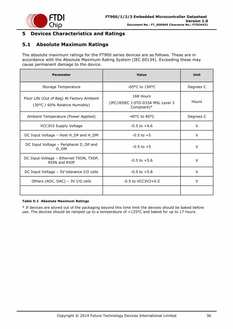
Copyright © 2014 Future Technology Devices International Limited 36
FT900/1/2/3 Embedded Microcontroller Datasheet Version 1.0
Document No.: FT_000965 Clearance No.: FTDI#421
5 Devices Characteristics and Ratings
5.1 Absolute Maximum Ratings
The absolute maximum ratings for the FT900 series devices are as follows. These are in
accordance with the Absolute Maximum Rating System (IEC 60134). Exceeding these may
cause permanent damage to the device.
Parameter Value Unit
Storage Temperature -65°C to 150°C Degrees C
Floor Life (Out of Bag) At Factory Ambient
(30°C / 60% Relative Humidity)
168 Hours
(IPC/JEDEC J-STD-033A MSL Level 3
Compliant)*
Hours
Ambient Temperature (Power Applied) -40°C to 85°C Degrees C
VCC3V3 Supply Voltage -0.5 to +4.6 V
DC Input Voltage – Host H_DP and H_DM -0.5 to +5 V
DC Input Voltage – Peripheral D_DP and
D_DM -0.5 to +5 V
DC Input Voltage – Ethernet TXON, TXOP, RXIN and RXIP
-0.5 to +5.6 V
DC Input Voltage – 5V tolerance I/O cells -0.5 to +5.8 V
Others (ADC, DAC) – 3V I/O cells -0.5 to VCC3V3+0.5 V
Table 5-1 Absolute Maximum Ratings
* If devices are stored out of the packaging beyond this time limit the devices should be baked before use. The devices should be ramped up to a temperature of +125°C and baked for up to 17 hours.
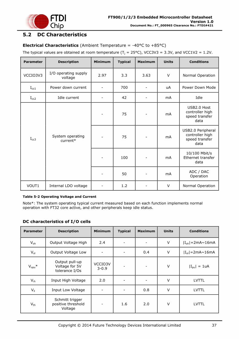
Copyright © 2014 Future Technology Devices International Limited 37
FT900/1/2/3 Embedded Microcontroller Datasheet Version 1.0
Document No.: FT_000965 Clearance No.: FTDI#421
5.2 DC Characteristics
Electrical Characteristics (Ambient Temperature = -40°C to +85°C)
The typical values are obtained at room temperature (Tj = 25°C), VCC3V3 = 3.3V, and VCC1V2 = 1.2V.
Parameter Description Minimum Typical Maximum Units Conditions
VCCIO3V3 I/O operating supply
voltage 2.97 3.3 3.63 V Normal Operation
Icc1 Power down current - 700 - uA Power Down Mode
Icc2 Idle current - 42 - mA Idle
Icc3
System operating current*
- 75 - mA
USB2.0 Host
controller high
speed transfer data
- 75 - mA
USB2.0 Peripheral
controller high speed transfer
data
- 100 - mA 10/100 Mbit/s
Ethernet transfer
data
- 50 - mA ADC / DAC Operation
VOUT1 Internal LDO voltage - 1.2 - V Normal Operation
Table 5-2 Operating Voltage and Current
Note*: The system operating typical current measured based on each function implements normal operation with FT32 core active, and other peripherals keep idle status.
DC characteristics of I/O cells
Parameter Description Minimum Typical Maximum Units Conditions
Voh Output Voltage High 2.4 - - V |Ioh|=2mA~16mA
Vol Output Voltage Low - - 0.4 V |Iol|=2mA~16mA
Vopu*
Output pull-up
Voltage for 5V tolerance I/Os
VCCIO3V
3-0.9 - - V |Ipu| = 1uA
Vih Input High Voltage 2.0 - - V LVTTL
Vil Input Low Voltage - - 0.8 V LVTTL
Vth Schmitt trigger
positive threshold Voltage
- 1.6 2.0 V LVTTL
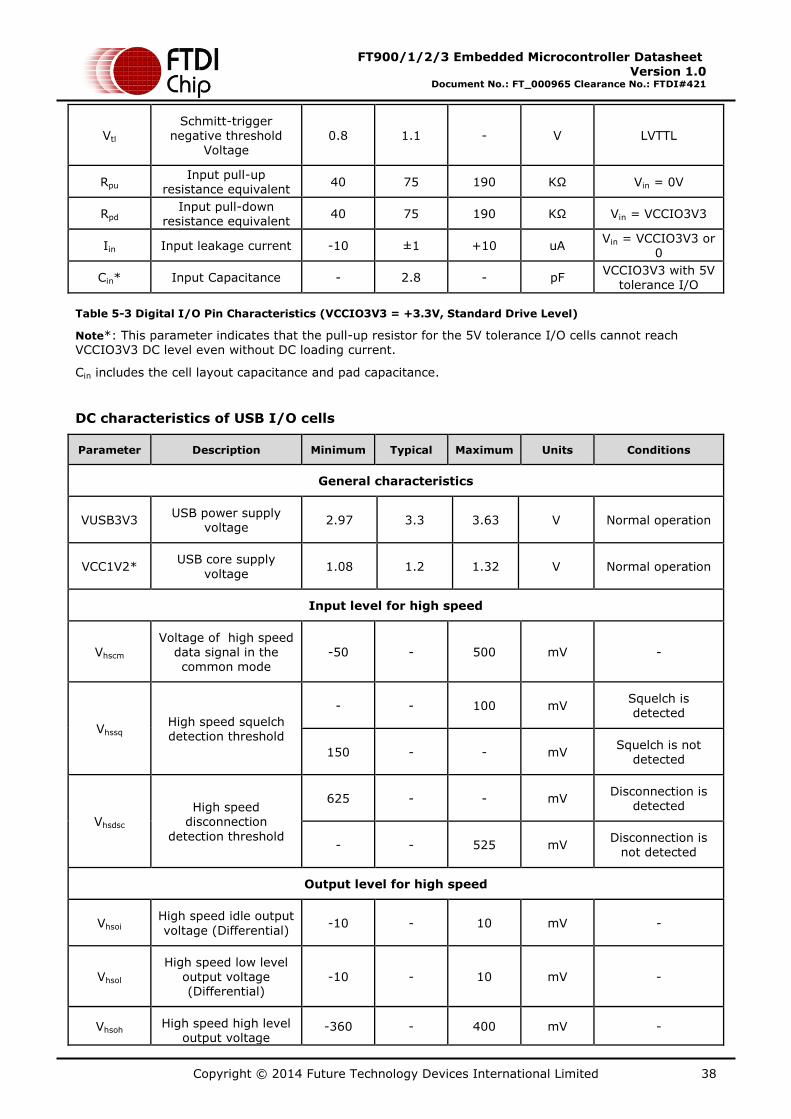
Copyright © 2014 Future Technology Devices International Limited 38
FT900/1/2/3 Embedded Microcontroller Datasheet Version 1.0
Document No.: FT_000965 Clearance No.: FTDI#421
Vtl Schmitt-trigger
negative threshold Voltage
0.8 1.1 - V LVTTL
Rpu Input pull-up
resistance equivalent 40 75 190 KΩ Vin = 0V
Rpd Input pull-down
resistance equivalent 40 75 190 KΩ Vin = VCCIO3V3
Iin Input leakage current -10 ±1 +10 uA Vin = VCCIO3V3 or
0
Cin* Input Capacitance - 2.8 - pF VCCIO3V3 with 5V
tolerance I/O
Table 5-3 Digital I/O Pin Characteristics (VCCIO3V3 = +3.3V, Standard Drive Level)
Note*: This parameter indicates that the pull-up resistor for the 5V tolerance I/O cells cannot reach VCCIO3V3 DC level even without DC loading current.
Cin includes the cell layout capacitance and pad capacitance.
DC characteristics of USB I/O cells
Parameter Description Minimum Typical Maximum Units Conditions
General characteristics
VUSB3V3 USB power supply
voltage 2.97 3.3 3.63 V Normal operation
VCC1V2* USB core supply
voltage 1.08 1.2 1.32 V Normal operation
Input level for high speed
Vhscm Voltage of high speed
data signal in the common mode
-50 - 500 mV -
Vhssq High speed squelch detection threshold
- - 100 mV Squelch is detected
150 - - mV Squelch is not
detected
Vhsdsc High speed
disconnection
detection threshold
625 - - mV Disconnection is
detected
- - 525 mV Disconnection is
not detected
Output level for high speed
Vhsoi High speed idle output
voltage (Differential) -10 - 10 mV -
Vhsol High speed low level
output voltage (Differential)
-10 - 10 mV -
Vhsoh High speed high level output voltage
-360 - 400 mV -

Copyright © 2014 Future Technology Devices International Limited 39
FT900/1/2/3 Embedded Microcontroller Datasheet Version 1.0
Document No.: FT_000965 Clearance No.: FTDI#421
Parameter Description Minimum Typical Maximum Units Conditions
(Differential)
Vchirpj Chirp-J output voltage
(Differential) 700 - 1100 mV -
Vchirpk Chirp-K output
voltage (Differential) -900 - -500 mV -
Input level for full speed and low speed
Vdi Differential input voltage sensitivity
0.2 - - V |Vdp-Vdm|
Vcm Differential common
mode voltage 0.8 - 2.5 V -
Vse Single ended receiver
threshold 0.8 - 2.0 V -
Output level for full speed and low speed
Vol Low level output
voltage 0 - 0.3 V -
Voh High level output
voltage 2.8 - 3.6 V -
Resistance
Rdrv Driver output impedance
40.5 45 49.5 ohm Equivalent
resistance used as
an internal chip
Table 5-4 USB I/O Pin (D_DP/D_DM, H_DP/H_DM) Characteristics
Note*: The VCC1V2 is USB Host or Peripheral transceiver core power supply input which need connect to external +1.2V voltage power while USB Host or Peripheral controller is active.
DC characteristics of Ethernet I/O cells
Parameter Description Minimum Typical Maximum Units Conditions
General characteristics
VETH3V3 Ethernet power supply
voltage 2.97 3.3 3.63 V Normal operation
VOUT2* Ethernet LDO voltage - 1.2 - V Normal operation
Total dissipative
power
10Base-TX mode
(Including TX current) - - 510 mW 10Base-TX mode
10Base-TX mode
(Excluding TX current) - - 147 mW 10Base-TX mode
100Base-TX mode - - 310 mW 100Base-TX mode
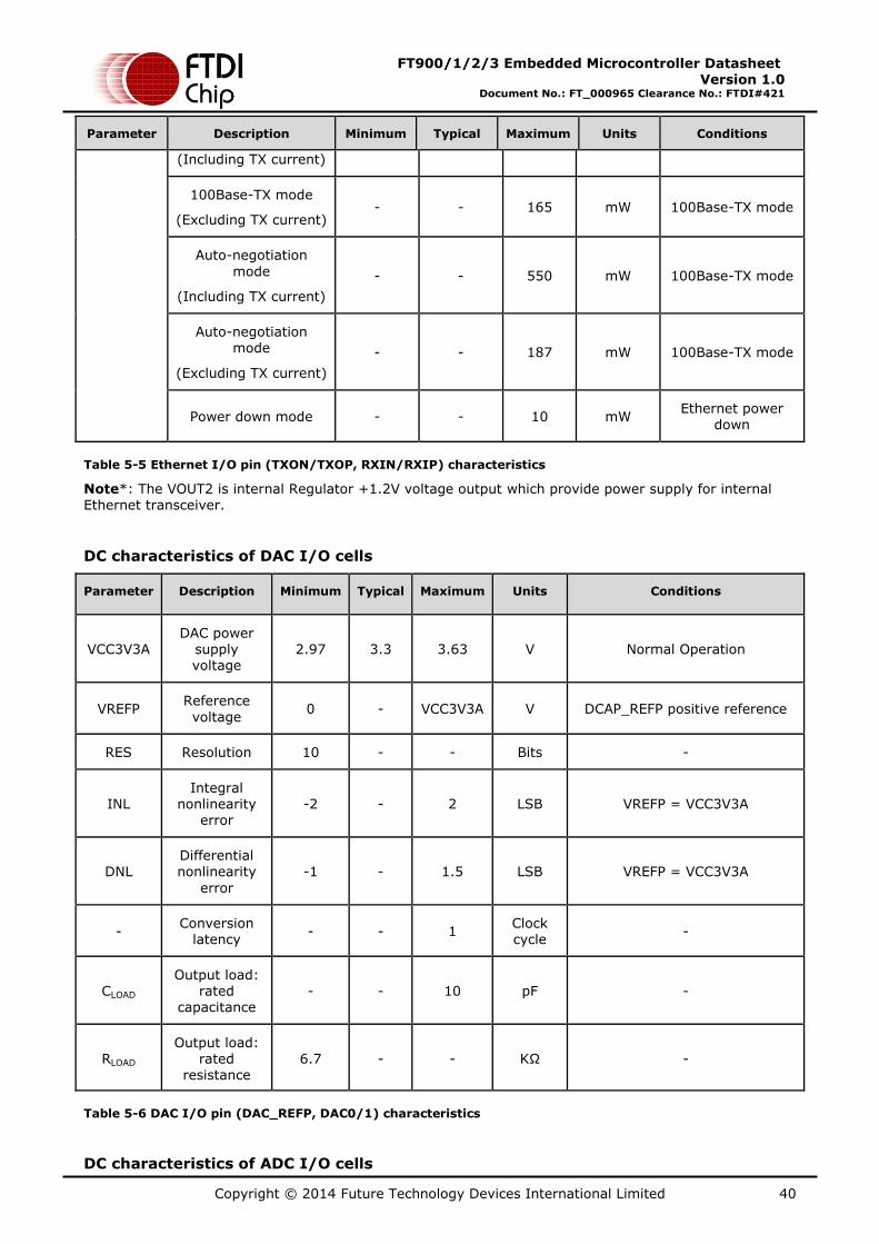
Copyright © 2014 Future Technology Devices International Limited 40
FT900/1/2/3 Embedded Microcontroller Datasheet Version 1.0
Document No.: FT_000965 Clearance No.: FTDI#421
Parameter Description Minimum Typical Maximum Units Conditions
(Including TX current)
100Base-TX mode
(Excluding TX current) - - 165 mW 100Base-TX mode
Auto-negotiation
mode
(Including TX current)
- - 550 mW 100Base-TX mode
Auto-negotiation mode
(Excluding TX current)
- - 187 mW 100Base-TX mode
Power down mode - - 10 mW Ethernet power
down
Table 5-5 Ethernet I/O pin (TXON/TXOP, RXIN/RXIP) characteristics
Note*: The VOUT2 is internal Regulator +1.2V voltage output which provide power supply for internal Ethernet transceiver.
DC characteristics of DAC I/O cells
Parameter Description Minimum Typical Maximum Units Conditions
VCC3V3A DAC power
supply voltage
2.97 3.3 3.63 V Normal Operation
VREFP Reference
voltage 0 - VCC3V3A V DCAP_REFP positive reference
RES Resolution 10 - - Bits -
INL Integral
nonlinearity error
-2 - 2 LSB VREFP = VCC3V3A
DNL Differential nonlinearity
error
-1 - 1.5 LSB VREFP = VCC3V3A
- Conversion
latency - - 1
Clock cycle
-
CLOAD Output load:
rated capacitance
- - 10 pF -
RLOAD Output load:
rated resistance
6.7 - - KΩ -
Table 5-6 DAC I/O pin (DAC_REFP, DAC0/1) characteristics
DC characteristics of ADC I/O cells
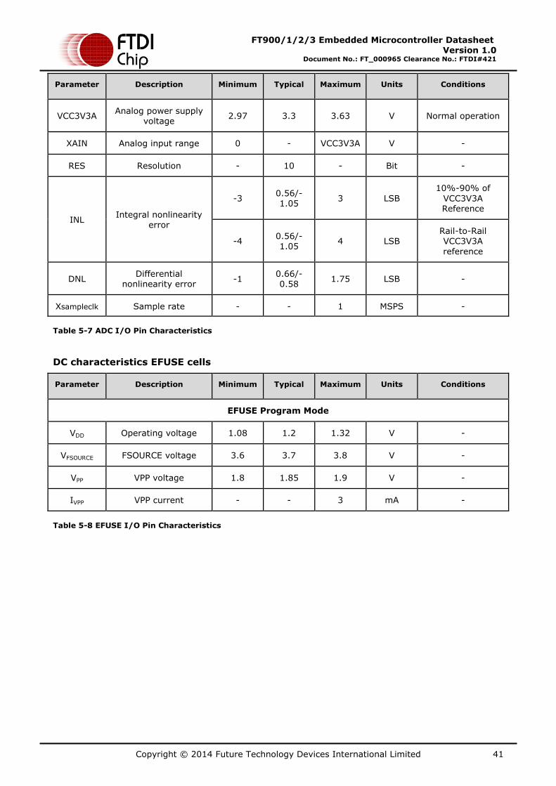
Copyright © 2014 Future Technology Devices International Limited 41
FT900/1/2/3 Embedded Microcontroller Datasheet Version 1.0
Document No.: FT_000965 Clearance No.: FTDI#421
Parameter Description Minimum Typical Maximum Units Conditions
VCC3V3A Analog power supply
voltage 2.97 3.3 3.63 V Normal operation
XAIN Analog input range 0 - VCC3V3A V -
RES Resolution - 10 - Bit -
INL Integral nonlinearity
error
-3 0.56/-1.05
3 LSB
10%-90% of
VCC3V3A Reference
-4 0.56/-1.05
4 LSB Rail-to-Rail VCC3V3A
reference
DNL Differential
nonlinearity error -1
0.66/-0.58
1.75 LSB -
Xsampleclk Sample rate - - 1 MSPS -
Table 5-7 ADC I/O Pin Characteristics
DC characteristics EFUSE cells
Parameter Description Minimum Typical Maximum Units Conditions
EFUSE Program Mode
VDD Operating voltage 1.08 1.2 1.32 V -
VFSOURCE FSOURCE voltage 3.6 3.7 3.8 V -
VPP VPP voltage 1.8 1.85 1.9 V -
IVPP VPP current - - 3 mA -
Table 5-8 EFUSE I/O Pin Characteristics

Copyright © 2014 Future Technology Devices International Limited 42
FT900/1/2/3 Embedded Microcontroller Datasheet Version 1.0
Document No.: FT_000965 Clearance No.: FTDI#421
5.3 AC Characteristics
AC Characteristics (Ambient Temperature = -40°C to +85°C)
System clock dynamic characteristics
Parameter
Value
Unit
Minimum Typical Maximum
Crystal oscillator
Clock frequency - 12.00 - MHz
External clock input
external clock
jitter - - 500 ps
clock duty cycle 45 50 55 %
Input voltage on pin XI/CLKIN
- 3.3 - V
Table 5-9 System clock characteristics
Note: Recommended accuracy of the clock frequency is 50ppm for the crystal.
RTC clock dynamic characteristics
Parameter
Value
Unit
Minimum Typical Maximum
Crystal oscillator
Clock frequency - 32768 - Hz
External clock input
external clock jitter - - 500 ps
clock duty cycle 45 50 55 %
Startup time - 0.5 5 s
Input voltage on pin RTC_XI/RTC_CLKIN
- 1.2 - V
Table 5-10 RTC clock characteristics
Analog USB I/O pins dynamic characteristics
Parameter Description Minimum Typical Maximum Units Conditions
Driver characteristic for high speed
Thsr High speed differential
rise time 500 - - ps -
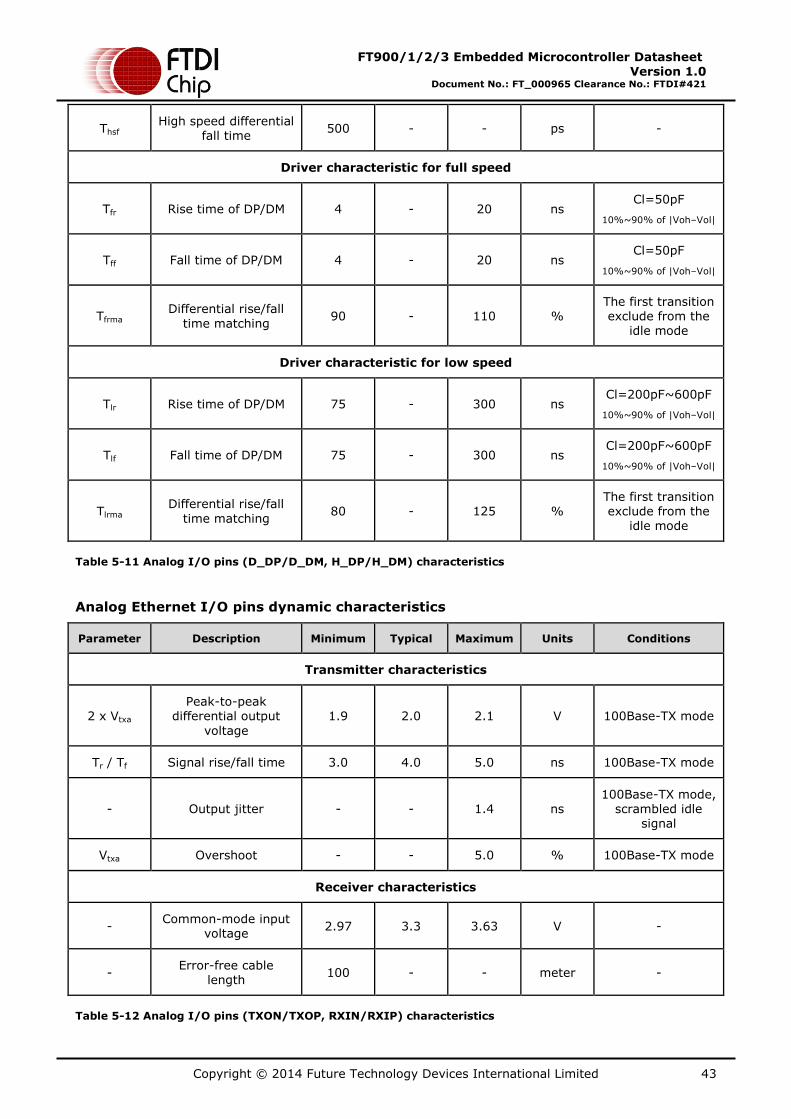
Copyright © 2014 Future Technology Devices International Limited 43
FT900/1/2/3 Embedded Microcontroller Datasheet Version 1.0
Document No.: FT_000965 Clearance No.: FTDI#421
Thsf High speed differential
fall time 500 - - ps -
Driver characteristic for full speed
Tfr Rise time of DP/DM 4 - 20 ns Cl=50pF
10%~90% of |Voh–Vol|
Tff Fall time of DP/DM 4 - 20 ns Cl=50pF
10%~90% of |Voh–Vol|
Tfrma Differential rise/fall
time matching 90 - 110 %
The first transition exclude from the
idle mode
Driver characteristic for low speed
Tlr Rise time of DP/DM 75 - 300 ns Cl=200pF~600pF
10%~90% of |Voh–Vol|
Tlf Fall time of DP/DM 75 - 300 ns Cl=200pF~600pF
10%~90% of |Voh–Vol|
Tlrma Differential rise/fall
time matching 80 - 125 %
The first transition exclude from the
idle mode
Table 5-11 Analog I/O pins (D_DP/D_DM, H_DP/H_DM) characteristics
Analog Ethernet I/O pins dynamic characteristics
Parameter Description Minimum Typical Maximum Units Conditions
Transmitter characteristics
2 x Vtxa Peak-to-peak
differential output
voltage
1.9 2.0 2.1 V 100Base-TX mode
Tr / Tf Signal rise/fall time 3.0 4.0 5.0 ns 100Base-TX mode
- Output jitter - - 1.4 ns 100Base-TX mode,
scrambled idle signal
Vtxa Overshoot - - 5.0 % 100Base-TX mode
Receiver characteristics
- Common-mode input
voltage 2.97 3.3 3.63 V -
- Error-free cable
length 100 - - meter -
Table 5-12 Analog I/O pins (TXON/TXOP, RXIN/RXIP) characteristics
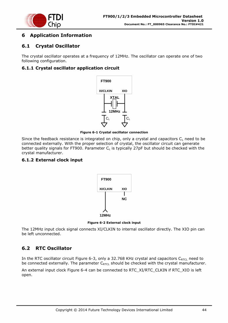
Copyright © 2014 Future Technology Devices International Limited 44
FT900/1/2/3 Embedded Microcontroller Datasheet Version 1.0
Document No.: FT_000965 Clearance No.: FTDI#421
6 Application Information
6.1 Crystal Oscillator
The crystal oscillator operates at a frequency of 12MHz. The oscillator can operate one of two
following configuration.
6.1.1 Crystal oscillator application circuit
FT900
XI/CLKIN XIO
XTAL
CL CL
12MHz
Figure 6-1 Crystal oscillator connection
Since the feedback resistance is integrated on chip, only a crystal and capacitors CL need to be
connected externally. With the proper selection of crystal, the oscillator circuit can generate
better quality signals for FT900. Parameter CL is typically 27pF but should be checked with the
crystal manufacturer.
6.1.2 External clock input
FT900
XI/CLKIN XIO
12MHz
NC
Figure 6-2 External clock input
The 12MHz input clock signal connects XI/CLKIN to internal oscillator directly. The XIO pin can
be left unconnected.
6.2 RTC Oscillator
In the RTC oscillator circuit Figure 6-3, only a 32.768 KHz crystal and capacitors CRTCL need to
be connected externally. The parameter CRTCL should be checked with the crystal manufacturer.
An external input clock Figure 6-4 can be connected to RTC_XI/RTC_CLKIN if RTC_XIO is left
open.
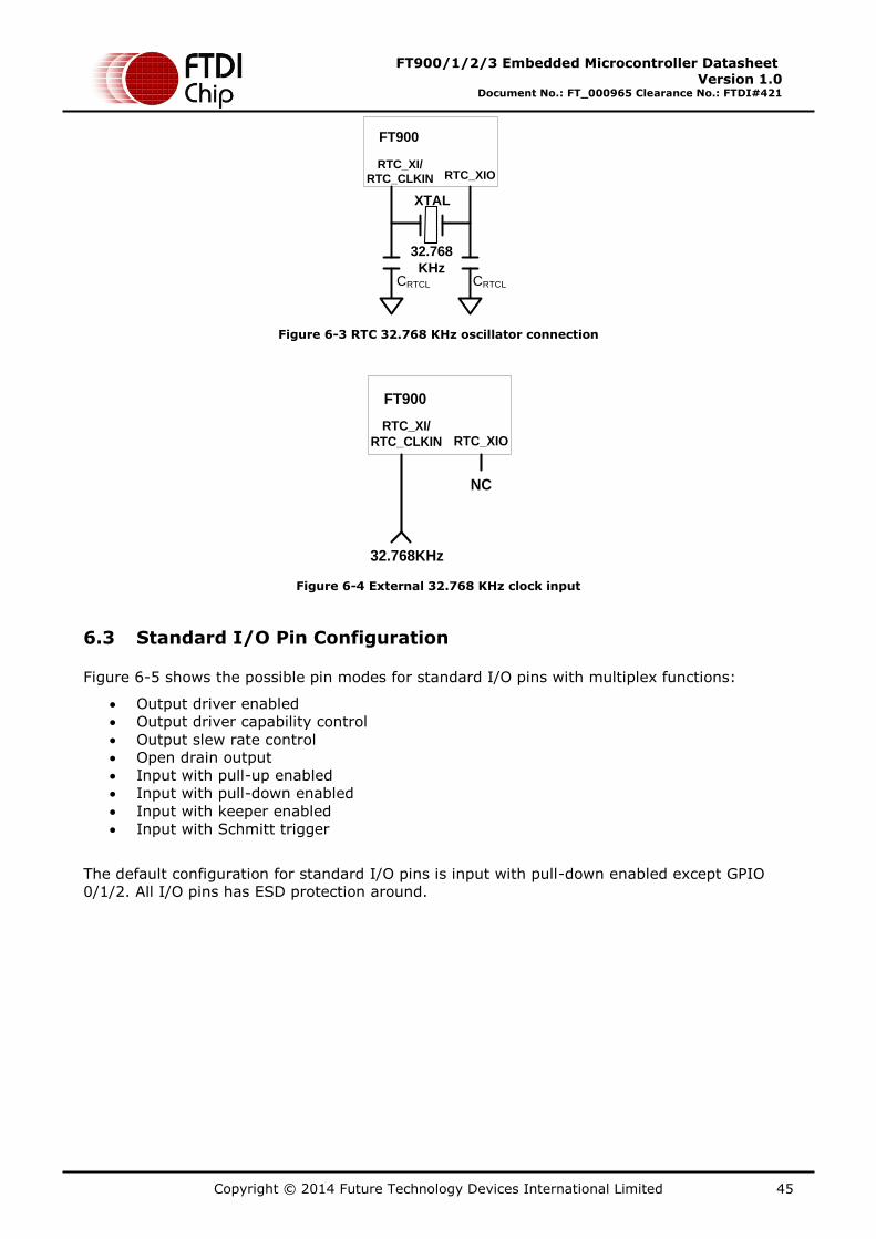
Copyright © 2014 Future Technology Devices International Limited 45
FT900/1/2/3 Embedded Microcontroller Datasheet Version 1.0
Document No.: FT_000965 Clearance No.: FTDI#421
FT900
RTC_XI/
RTC_CLKIN RTC_XIO
XTAL
CRTCL CRTCL
32.768
KHz
Figure 6-3 RTC 32.768 KHz oscillator connection
FT900
RTC_XI/
RTC_CLKIN RTC_XIO
32.768KHz
NC
Figure 6-4 External 32.768 KHz clock input
6.3 Standard I/O Pin Configuration
Figure 6-5 shows the possible pin modes for standard I/O pins with multiplex functions:
Output driver enabled
Output driver capability control
Output slew rate control
Open drain output
Input with pull-up enabled
Input with pull-down enabled
Input with keeper enabled
Input with Schmitt trigger
The default configuration for standard I/O pins is input with pull-down enabled except GPIO
0/1/2. All I/O pins has ESD protection around.
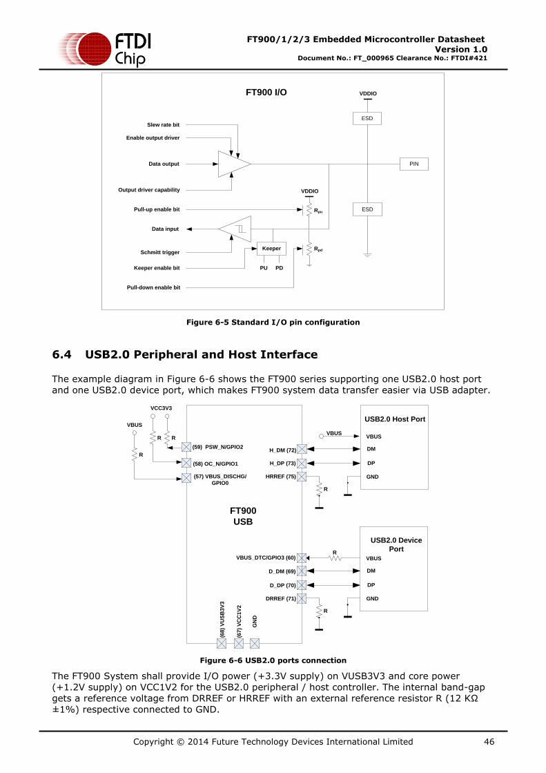
Copyright © 2014 Future Technology Devices International Limited 46
FT900/1/2/3 Embedded Microcontroller Datasheet Version 1.0
Document No.: FT_000965 Clearance No.: FTDI#421
Slew rate bit
Enable output driver
Data output
Output driver capability
Data input
Schmitt triggerKeeper
PU PDKeeper enable bit
Pull-down enable bit
Pull-up enable bit Rpu
Rpd
ESD
ESD
VDDIO
VDDIO
PIN
FT900 I/O
Figure 6-5 Standard I/O pin configuration
6.4 USB2.0 Peripheral and Host Interface
The example diagram in Figure 6-6 shows the FT900 series supporting one USB2.0 host port
and one USB2.0 device port, which makes FT900 system data transfer easier via USB adapter.
USB2.0 Device
PortVBUS_DTC/GPIO3 (60) VBUS
D_DM (69)
D_DP (70)
DM
DP
GNDDRREF (71)
R
R
USB2.0 Host Port
FT900
USB
(59) PSW_N/GPIO2
VBUS
H_DM (72)
H_DP (73)
DM
DP
GN
D
GNDHRREF (75)
(67
) V
CC
1V
2
(68
) V
US
B3
V3
R
(58) OC_N/GPIO1
(57) VBUS_DISCHG/
GPIO0
VBUSRR
VCC3V3
R
VBUS
Figure 6-6 USB2.0 ports connection
The FT900 System shall provide I/O power (+3.3V supply) on VUSB3V3 and core power
(+1.2V supply) on VCC1V2 for the USB2.0 peripheral / host controller. The internal band-gap
gets a reference voltage from DRREF or HRREF with an external reference resistor R (12 KΩ
±1%) respective connected to GND.
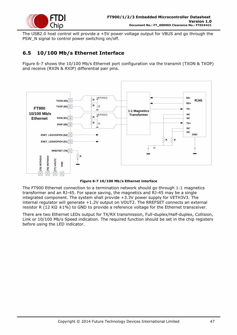
Copyright © 2014 Future Technology Devices International Limited 47
FT900/1/2/3 Embedded Microcontroller Datasheet Version 1.0
Document No.: FT_000965 Clearance No.: FTDI#421
The USB2.0 host control will provide a +5V power voltage output for VBUS and go through the
PSW_N signal to control power switching on/off.
6.5 10/100 Mb/s Ethernet Interface
Figure 6-7 shows the 10/100 Mb/s Ethernet port configuration via the transmit (TXON & TXOP)
and receive (RXIN & RXIP) differential pair pins.
RXIN (81)
RXIP (80)
RJ45
10/100 Mb/s
Ethernet
RD-
TXON (83)
TXOP (82)
GN
D
GND
RREFSET (78)
(77)
VO
UT
2
(76)
VE
TH
3V
3 R
FT900
ENET_LED1/GPIO5 (62)
ENET_LED0/GPIO4 (61)
(79)
VE
TH
3V
3
R
R
R
R
R C
VETH3V3
VETH3V3
1:1 Magnetics
Transformer
RD+
TD-
TD+
NC
NC
NC
NC
R
C
C
Figure 6-7 10/100 Mb/s Ethernet interface
The FT900 Ethernet connection to a termination network should go through 1:1 magnetics
transformer and an RJ-45. For space saving, the magnetics and RJ-45 may be a single
integrated component. The system shall provide +3.3V power supply for VETH3V3. The
internal regulator will generate +1.2V output on VOUT2. The RREFSET connects an external
resistor R (12 KΩ ±1%) to GND to provide a reference voltage for the Ethernet transceiver.
There are two Ethernet LEDs output for TX/RX transmission, Full-duplex/Half-duplex, Collision,
Link or 10/100 Mb/s Speed indication. The required function should be set in the chip registers
before using the LED indicator.
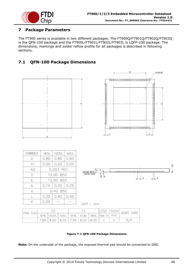
Copyright © 2014 Future Technology Devices International Limited 48
FT900/1/2/3 Embedded Microcontroller Datasheet Version 1.0
Document No.: FT_000965 Clearance No.: FTDI#421
7 Package Parameters
The FT900 series is available in two different packages. The FT900Q/FT901Q/FT902Q/FT903Q
is the QFN-100 package and the FT900L/FT901L/FT902L/FT903L is LQFP-100 package. The
dimensions, markings and solder reflow profile for all packages is described in following
sections.
7.1 QFN-100 Package Dimensions
Figure 7-1 QFN-100 Package Dimensions
Note: On the underside of the package, the exposed thermal pad should be connected to GND.
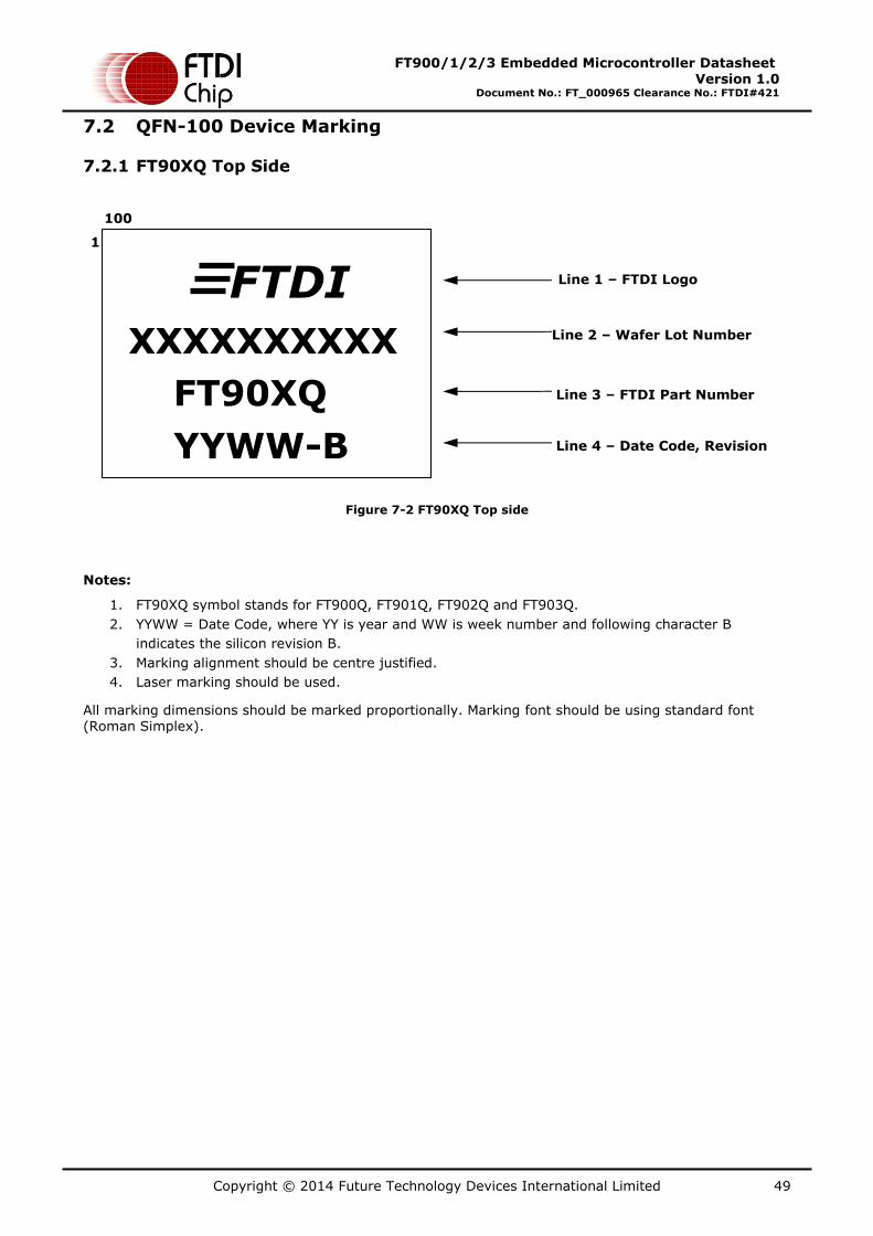
Copyright © 2014 Future Technology Devices International Limited 49
FT900/1/2/3 Embedded Microcontroller Datasheet Version 1.0
Document No.: FT_000965 Clearance No.: FTDI#421
7.2 QFN-100 Device Marking
7.2.1 FT90XQ Top Side
Figure 7-2 FT90XQ Top side
Notes:
1. FT90XQ symbol stands for FT900Q, FT901Q, FT902Q and FT903Q.
2. YYWW = Date Code, where YY is year and WW is week number and following character B
indicates the silicon revision B. 3. Marking alignment should be centre justified. 4. Laser marking should be used.
All marking dimensions should be marked proportionally. Marking font should be using standard font (Roman Simplex).
FTDI
XXXXXXXXXX
FT90XQ
Line 1 – FTDI Logo
Line 4 – Date Code, Revision
Line 2 – Wafer Lot Number
1
100
Line 3 – FTDI Part Number
YYWW-B
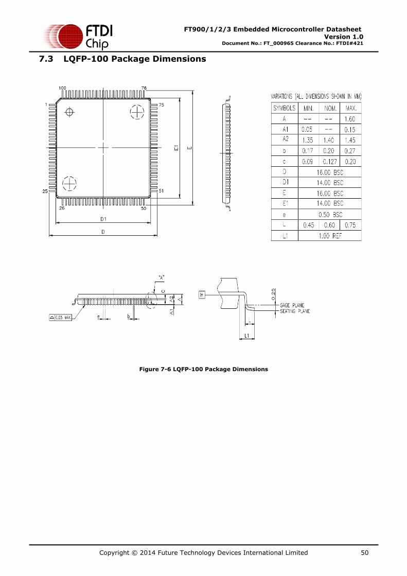
Copyright © 2014 Future Technology Devices International Limited 50
FT900/1/2/3 Embedded Microcontroller Datasheet Version 1.0
Document No.: FT_000965 Clearance No.: FTDI#421
7.3 LQFP-100 Package Dimensions
Figure 7-6 LQFP-100 Package Dimensions
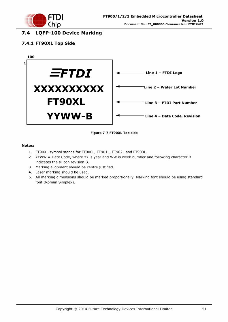
Copyright © 2014 Future Technology Devices International Limited 51
FT900/1/2/3 Embedded Microcontroller Datasheet Version 1.0
Document No.: FT_000965 Clearance No.: FTDI#421
7.4 LQFP-100 Device Marking
7.4.1 FT90XL Top Side
Figure 7-7 FT90XL Top side
Notes:
1. FT90XL symbol stands for FT900L, FT901L, FT902L and FT903L.
2. YYWW = Date Code, where YY is year and WW is week number and following character B
indicates the silicon revision B. 3. Marking alignment should be centre justified. 4. Laser marking should be used. 5. All marking dimensions should be marked proportionally. Marking font should be using standard
font (Roman Simplex).
FTDI
XXXXXXXXXX
FT90XL
Line 1 – FTDI Logo
Line 4 – Date Code, Revision
Line 2 – Wafer Lot Number
1
100
Line 3 – FTDI Part Number
YYWW-B
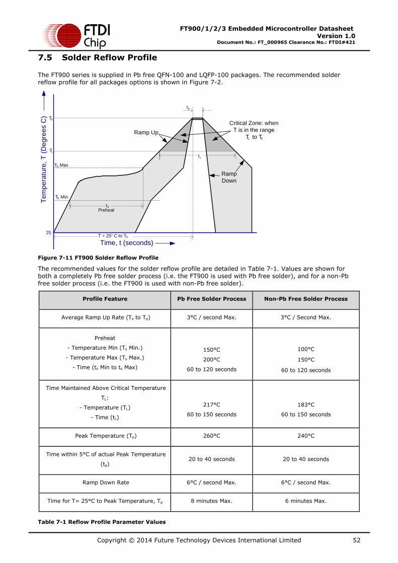
Copyright © 2014 Future Technology Devices International Limited 52
FT900/1/2/3 Embedded Microcontroller Datasheet Version 1.0
Document No.: FT_000965 Clearance No.: FTDI#421
7.5 Solder Reflow Profile
The FT900 series is supplied in Pb free QFN-100 and LQFP-100 packages. The recommended solder reflow profile for all packages options is shown in Figure 7-2.
Figure 7-11 FT900 Solder Reflow Profile
The recommended values for the solder reflow profile are detailed in Table 7-1. Values are shown for both a completely Pb free solder process (i.e. the FT900 is used with Pb free solder), and for a non-Pb
free solder process (i.e. the FT900 is used with non-Pb free solder).
Profile Feature Pb Free Solder Process Non-Pb Free Solder Process
Average Ramp Up Rate (Ts to Tp) 3°C / second Max. 3°C / Second Max.
Preheat
- Temperature Min (Ts Min.)
- Temperature Max (Ts Max.)
- Time (ts Min to ts Max)
150°C
200°C
60 to 120 seconds
100°C
150°C
60 to 120 seconds
Time Maintained Above Critical Temperature
TL:
- Temperature (TL)
- Time (tL)
217°C
60 to 150 seconds
183°C
60 to 150 seconds
Peak Temperature (Tp) 260°C 240°C
Time within 5°C of actual Peak Temperature
(tp) 20 to 40 seconds 20 to 40 seconds
Ramp Down Rate 6°C / second Max. 6°C / second Max.
Time for T= 25°C to Peak Temperature, Tp 8 minutes Max. 6 minutes Max.
Table 7-1 Reflow Profile Parameter Values
Critical Zone: when
T is in the range
T to T
Te
mpera
ture
, T
(D
eg
ree
s C
)
Time, t (seconds)
25PT = 25º C to T
tp
Tp
TL
tPreheat
S
tL
Ramp UpL p
Ramp
Down
T MaxS
T MinS
Copyright © 2014 Future Technology Devices International Limited 53
FT900/1/2/3 Embedded Microcontroller Datasheet Version 1.0
Document No.: FT_000965 Clearance No.: FTDI#421
8 Abbreviations
Acronym Description
ADC Analog-to-Digital Converter
BCD Battery Charge Device
CAN Controller Area Network
CDP Charging Downstream Port
CPI Camera Parallel Interface
DAC Digital-to-Analog Converter
DAQ Data Acquisition
DCP Dedicated Charging Port
DNL Differential Nonlinearity
FIFO First In First Out
GPIO General Purpose Input / Output
INL Integral Nonlinearity
I/O Input / Output
LQFP Low profile Quad Flat Package
LSB Least Significant Bit
MMC Multimedia Card
MSPS Mega Samples Per Second
NMI Non-Maskable Interrupt input
POR Power On Reset
PWM Pulse Width Modulator
QFN Quad Flat No-Lead
RTC Real Time Clock
Copyright © 2014 Future Technology Devices International Limited 54
FT900/1/2/3 Embedded Microcontroller Datasheet Version 1.0
Document No.: FT_000965 Clearance No.: FTDI#421
SD Secure Digital
SDIO Secure Digital Input Output
SDP Standard Downstream Port
SPI Serial Peripheral Interface
UART Universal Asynchronous Receiver/Transmitter
UHS Ultra High Speed
USB Universal Serial Bus
Table 8-1 Abbreviations
Copyright © 2014 Future Technology Devices International Limited 55
FT900/1/2/3 Embedded Microcontroller Datasheet Version 1.0
Document No.: FT_000965 Clearance No.: FTDI#421
9 FTDI Chip Contact Information
Head Office – Glasgow, UK Unit 1, 2 Seaward Place, Centurion Business Park Glasgow G41 1HH United Kingdom Tel: +44 (0) 141 429 2777 Fax: +44 (0) 141 429 2758 E-mail (Sales) [email protected] E-mail (Support) [email protected] E-mail (General Enquiries) [email protected]
Branch Office – Taipei, Taiwan 2F, No. 516, Sec. 1, NeiHu Road Taipei 114 Taiwan, R.O.C. Tel: +886 (0) 2 8797 1330 Fax: +886 (0) 2 8751 9737 E-mail (Sales) [email protected] E-mail (Support) [email protected] E-mail (General Enquiries) [email protected]
Branch Office – Tigard, Oregon, USA 7130 SW Fir Loop Tigard, OR 97223 USA Tel: +1 (503) 547 0988 Fax: +1 (503) 547 0987 E-Mail (Sales) [email protected] E-Mail (Support) [email protected] E-Mail (General Enquiries) [email protected]
Branch Office – Shanghai, China Room 1103, No. 666 West Huaihai Road, Changning District Shanghai, 200052 China Tel: +86 21 62351596 Fax: +86 21 62351595 E-mail (Sales) [email protected] E-mail (Support) [email protected] E-mail (General Enquiries) [email protected]
Web Site http://ftdichip.com
System and equipment manufacturers and designers are responsible to ensure that their systems, and any Future Technology
Devices International Ltd (FTDI) devices incorporated in their systems, meet all applicable safety, regulatory and system-level
performance requirements. All application-related information in this document (including application descriptions, suggested
FTDI devices and other materials) is provided for reference only. While FTDI has taken care to assure it is accurate, this
information is subject to customer confirmation, and FTDI disclaims all liability for system designs and for any applications
assistance provided by FTDI. Use of FTDI devices in life support and/or safety applications is entirely at the user’s risk, and the user agrees to defend, indemnify and hold harmless FTDI from any and all damages, claims, suits or expense resulting from
such use. This document is subject to change without notice. No freedom to use patents or other intellectual property rights is
implied by the publication of this document. Neither the whole nor any part of the information contained in, or the product
described in this document, may be adapted or reproduced in any material or electronic form without the prior written consent
of the copyright holder. Future Technology Devices International Ltd, Unit 1, 2 Seaward Place, Centurion Business Park,
Glasgow G41 1HH, United Kingdom. Scotland Registered Company Number: SC136640

Copyright © 2014 Future Technology Devices International Limited 56
FT900/1/2/3 Embedded Microcontroller Datasheet Version 1.0
Document No.: FT_000965 Clearance No.: FTDI#421
Appendix A – References
Useful Application Notes
AN 324: FT900_User_Manual
Appendix B - List of Figures and Tables
List of Figures
Figure 2-1 FT900 Block Diagram ..................................................................................................... 4
Figure 3-1 Pin Configuration FT900Q (top-down view) ....................................................................... 8
Figure 3-2 Pin Configuration FT901Q (top-down view) ....................................................................... 9
Figure 3-3 Pin Configuration FT902Q (top-down view) ..................................................................... 10
Figure 3-4 Pin Configuration FT903Q (top-down view) ..................................................................... 11
Figure 3-5 Pin Configuration FT900L (top-down view) ..................................................................... 12
Figure 3-6 Pin Configuration FT901L (top-down view) ..................................................................... 13
Figure 3-7 Pin Configuration FT902L (top-down view) ..................................................................... 14
Figure 3-8 Pin Configuration FT903L (top-down view) ..................................................................... 15
Figure 6-1 Crystal oscillator connection ......................................................................................... 44
Figure 6-2 External clock input ..................................................................................................... 44
Figure 6-3 RTC 32.768 KHz oscillator connection ............................................................................ 45
Figure 6-4 External 32.768 KHz clock input .................................................................................... 45
Figure 6-5 Standard I/O pin configuration ...................................................................................... 46
Figure 6-6 USB2.0 ports connection .............................................................................................. 46
Figure 6-7 10/100 Mb/s Ethernet interface ..................................................................................... 47
Figure 7-1 QFN-100 Package Dimensions ....................................................................................... 48
Figure 7-2 FT90XQ Top side ......................................................................................................... 49
Figure 7-6 LQFP-100 Package Dimensions ..................................................................................... 50
Figure 7-7 FT90XL Top side .......................................................................................................... 51
Figure 7-11 FT900 Solder Reflow Profile ........................................................................................ 52
List of Tables
Table 1-1 FT900 Series Part Numbers ............................................................................................. 3
Table 3-1 FT900 pin description .................................................................................................... 23
Table 4-1 FT900 series default interrupt priority ............................................................................. 26
Table 4-2 FT900 series I/O memory mapping ................................................................................. 27
Table 5-1 Absolute Maximum Ratings ........................................................................................... 36
Table 5-2 Operating Voltage and Current ....................................................................................... 37
Table 5-3 Digital I/O Pin Characteristics (VCCIO3V3 = +3.3V, Standard Drive Level) .......................... 38
Table 5-4 USB I/O Pin (D_DP/D_DM, H_DP/H_DM) Characteristics ................................................... 39
Table 5-5 Ethernet I/O pin (TXON/TXOP, RXIN/RXIP) characteristics ................................................. 40
Table 5-6 DAC I/O pin (DAC_REFP, DAC0/1) characteristics ............................................................. 40
Table 5-7 ADC I/O Pin Characteristics ........................................................................................... 41
Table 5-8 EFUSE I/O Pin Characteristics ........................................................................................ 41
Copyright © 2014 Future Technology Devices International Limited 57
FT900/1/2/3 Embedded Microcontroller Datasheet Version 1.0
Document No.: FT_000965 Clearance No.: FTDI#421
Table 5-9 System clock characteristics .......................................................................................... 42
Table 5-10 RTC clock characteristics ............................................................................................. 42
Table 5-11 Analog I/O pins (D_DP/D_DM, H_DP/H_DM) characteristics ............................................. 43
Table 5-12 Analog I/O pins (TXON/TXOP, RXIN/RXIP) characteristics ................................................ 43
Table 7-1 Reflow Profile Parameter Values ..................................................................................... 52
Table 8-1 Abbreviations ............................................................................................................... 54
Copyright © 2014 Future Technology Devices International Limited 58
FT900/1/2/3 Embedded Microcontroller Datasheet Version 1.0
Document No.: FT_000965 Clearance No.: FTDI#421
Appendix C - Revision History
Document Title: FT900/1/2/3 Embedded Microcontroller Datasheet
Document Reference No.: FT_000965
Clearance No.: FTDI#421
Product Page: http://www.ftdichip.com/FTProducts.htm
Document Feedback: DS_FT900_1_2_3
Version 1.0 Initial release 24 Feb 2014
Version 1.0 Full release 07 Nov 2014