FT900 User Manual - Bridgetek – Welcome to...
219
Use of Bridgetek devices in life support and/or safety applications is entirely at the user’s risk, and the user agrees to defend, indemnify and hold Bridgetek harmless from any and all damages, claims, suits or expense resulting from such use. Bridgetek Pte Ltd (BRT Chip) 178 Paya Lebar Road, #07-03, Singapore 409030 Tel: +65 6547 4827 Fax: +65 6841 6071 Web Site: http://www.brtchip.com Copyright © Bridgetek Pte Ltd Application Note AN_324 FT900 User Manual Version 1.2 Issue Date: 2017-03-30 This document provides details about the peripherals of the FT900 as well as the general system registers
Transcript of FT900 User Manual - Bridgetek – Welcome to...

Use of Bridgetek devices in life support and/or safety applications is entirely at the user’s risk, and the user agrees to defend, indemnify and hold Bridgetek harmless from any and all damages,
claims, suits or expense resulting from such use.
Bridgetek Pte Ltd (BRT Chip) 178 Paya Lebar Road, #07-03, Singapore 409030
Tel: +65 6547 4827 Fax: +65 6841 6071 Web Site: http://www.brtchip.com
Copyright © Bridgetek Pte Ltd
Application Note
AN_324
FT900 User Manual
Version 1.2
Issue Date: 2017-03-30
This document provides details about the peripherals of the FT900 as well as the general system registers
Application Note
AN_324 FT900 User Manual Version 1.2
Document Reference No.: BRT_000131 Clearance No.: BRT#081
1 Product Page Document Feedback Copyright © Bridgetek Pte Ltd
Table of Contents
1 Introduction .............................................................. 15
2 FT900 System Architecture ....................................... 16
2.1 Architecture overview ......................................................... 16
2.2 Memory organization .......................................................... 17
2.3 FT900 Boot Control ............................................................. 17
2.4 Debugging Support ............................................................. 18
3 Register Map ............................................................. 19
4 Notations .................................................................. 21
5 General System Registers ......................................... 22
5.1 Register Summary............................................................... 22
5.2 Register Details ................................................................... 24
5.2.1 HIPID - Chip ID Register (address offset: 0x00) .................................................... 24
5.2.2 EFCFG - Chip Configuration Register (address offset: 0x04) .................................... 24
5.2.3 CLKCFG - Clock Configuration Register (address offset: 0x08) ................................. 25
5.2.4 PMCFG - Power Management Register (address offset: 0x0C) .................................. 25
5.2.5 PTSTNSET - Test & Set Register (address offset: 0x10) .......................................... 27
5.2.6 PTSTNSETR - Test & Set Shadow Register (address offset: 0x14) ............................ 27
5.2.7 MSC0CFG - Miscellaneous Configuration Register (address offset: 0x18) ................... 27
5.2.8 GPIO Pin Configuration Registers (address offset: 0x1C – 0x5F) .............................. 29
5.2.9 GPIO Configuration Registers (address offset: 0x60 – 0x83) ................................... 34
5.2.10 GPIO Value Registers (address offset: 0x84 – 0x8F) ............................................. 37
5.2.11 GPIO Interrupt Enable Registers (address offset: 0x90 – 0x9B) ............................. 38
5.2.12 Interrupt Pending Registers (address offset: 0x9C – 0xA7) .................................... 38
5.2.13 ETH_PHY_CFG - Ethernet PHY Miscellaneous Configuration Register (address offset:
0xA8) ....................................................................................................................... 39
5.2.14 ETH_PHY_ID - Ethernet PHY ID Register (address offset: 0xAC) ............................. 39
5.2.15 DAC_ADC_CONF - ADC/DAC Configuration/Status Register (address offset: 0xB0) ... 39
5.2.16 DAC_ADC_CNT - ADC/DAC Count Register (address offset: 0xB4) .......................... 41
5.2.17 DAC_ADC_DATA - ADC/DAC Data Register (address offset: 0xB8) ......................... 41
6 Interrupt Controller .................................................. 42
Application Note
AN_324 FT900 User Manual Version 1.2
Document Reference No.: BRT_000131 Clearance No.: BRT#081
2 Product Page Document Feedback Copyright © Bridgetek Pte Ltd
6.1 Register Summary............................................................... 43
6.2 Register Details ................................................................... 44
6.2.1 IRQ00-03 Assignment Register (address offset: 0x00) ............................................ 44
6.2.2 IRQ04-07 Assignment Register (address offset: 0x04) ............................................ 44
6.2.3 IRQ08-11 Assignment Register (address offset: 0x08) ............................................ 44
6.2.4 IRQ12-15 Assignment Register (address offset: 0x0C) ........................................... 45
6.2.5 IRQ16-19 Assignment Register (address offset: 0x10) ............................................ 45
6.2.6 IRQ20-23 Assignment Register (address offset: 0x14) ............................................ 45
6.2.7 IRQ24-27 Assignment Register (address offset: 0x18) ............................................ 45
6.2.8 IRQ28-31 Assignment Register (address offset: 0x1C) ........................................... 46
6.2.9 IRQ Control Register (address offset: 0x20) .......................................................... 46
7 EFUSE ....................................................................... 47
7.1 Introduction ........................................................................ 47
7.2 EFUSE Operation ................................................................. 47
7.3 EFUSE bits ........................................................................... 47
8 USB Host ................................................................... 49
8.1 Register Summary............................................................... 49
8.2 EHCI Operational Registers ................................................. 50
8.2.1 HC Capability Register (address offset: 0x00) ........................................................ 50
8.2.2 HCSPARAMS – HC Structural Parameters (address offset: 0x04) .............................. 50
8.2.3 HCCPARAMS – HC Capability Parameters (address offset: 0x08) .............................. 50
8.2.4 USBCMD – HC USB Command Register (address offset: 0x10) ................................ 51
8.2.5 USBSTS – HC USB Status Register (address offset: 0x14) ....................................... 52
8.2.6 USBINTR – HC USB Interrupt Enable Register (address offset: 0x18) ....................... 53
8.2.7 FRINDEX – HC Frame Index Register (address offset: 0x1C) ................................... 54
8.2.8 PERIODICLISTBASE – HC Periodic Frame List Base Address Register (address offset:
0x24) ....................................................................................................................... 54
8.2.9 ASYNCLISTADDR – HC Current Asynchronous List Address Register (address offset:
0x28) ....................................................................................................................... 54
8.2.10 PORTSC – HC Port Status and Control Register (address offset: 0x30) .................... 55
8.3 Configuration Registers ...................................................... 56
8.3.1 EOF Time & Asynchronous Schedule Sleep Timer Register (address offset: 0x34) ...... 56
8.3.2 Bus Monitor Control / Status Register (address offset: 0x40) ................................... 58
8.3.3 HPROT – Master Protection Information Setting Register (address offset: 0x78) ........ 59
Application Note
AN_324 FT900 User Manual Version 1.2
Document Reference No.: BRT_000131 Clearance No.: BRT#081
3 Product Page Document Feedback Copyright © Bridgetek Pte Ltd
8.4 USB Host Testing Registers ................................................. 59
8.4.1 Vendor Specific IO Control Register (address offset: 0x54) ..................................... 59
8.4.2 Vendor Specific Status Register (address offset: 0x58) ........................................... 59
8.4.3 Test Register (address offset: 0x50)..................................................................... 59
8.4.4 HC_RSRV1 - Reserved 1 Register (address offset: 0x70) ........................................ 60
8.4.5 HC_RSRV2 - Reserved 2 Register (address offset: 0x74) ....................................... 60
9 USB peripheral .......................................................... 61
9.1 Register Summary............................................................... 61
9.2 Initialization Registers ........................................................ 63
9.2.1 DC_ADDRESS_ENABLE – Address Register (address offset: 0x18) ........................... 63
9.2.2 DC_MODE – Mode Register (address offset: 0x10) ................................................. 63
9.2.3 DC_INT_ENABLE – Interrupt Enable Register (address offset: 0x08) ........................ 63
9.2.4 DC_EP_INT_ENABLE – Endpoints Interrupt Enable Register (address offset: 0x0C) .... 64
9.3 Control Endpoint Data flow Registers .................................. 64
9.3.1 DC_EP0_CONTROL – Endpoint 0 Control Register (address offset: 0x1C) .................. 64
9.3.2 DC_EP0_STATUS – Endpoint 0 Status Register (address offset: 0x20) ...................... 64
9.3.3 DC_EP0_BUFFER_LENGTH – Endpoint 0 Buffer Length Register (address offset: 0x24) 65
9.3.4 DC_EP0_BUFFER – Endpoint 0 Buffer Register (address offset: 0x28) ....................... 65
9.4 Other Endpoint Data Flow Registers .................................... 66
9.4.1 DC_EP(x)_CONTROL – Endpoint Control Registers (address offset:
0x2C/0x3C/0x4C/0x5C/0x6C/0x7C/0x8C) ..................................................................... 66
9.4.2 DC_EP(x)_STATUS – Endpoint Status Registers (address offset:
0x30/0x40/0x50/0x60/0x70/0x80/0x90) ...................................................................... 66
9.4.3 DC_EP(x)_BUFFER_LENGTH_LSB – Endpoint Buffer Length LSB Registers (address
offset: 0x34/0x44/0x54/0x64/0x74/0x84/0x94) ............................................................ 68
9.4.4 DC_EP(x)_BUFFER_LENGTH_MSB – Endpoint Buffer Length MSB Registers (address
offset: 0x35/0x45/0x55/0x65/0x75/0x85/0x95) ............................................................ 68
9.4.5 DC_EP(x)_BUFFER – Endpoint Buffer Registers (address offset:
0x38/0x48/0x58/0x68/0x78/0x88/0x98) ...................................................................... 68
9.5 General Registers ................................................................ 68
9.5.1 DC_INT_STATUS – Interrupt Status Register (address offset: 0x00) ........................ 68
9.5.2 DC_EP_INT_STATUS – Endpoints Interrupt Status Register (address offset: 0x04)..... 69
9.5.3 DC_FRAME_NUMBER_LSB – Frame Number LSB Register (address offset: 0x14) ....... 69
9.5.4 DC_FRAME_NUMBER_MSB – Frame Number MSB Register (address offset: 0x15) ...... 69
10 Ethernet .................................................................. 70

Application Note
AN_324 FT900 User Manual Version 1.2
Document Reference No.: BRT_000131 Clearance No.: BRT#081
4 Product Page Document Feedback Copyright © Bridgetek Pte Ltd
10.1 Register Summary ............................................................. 71
10.2 Register Details ................................................................. 72
10.2.1 ETH_INT_STATUS – Interrupt Status Register (address offset: 0x0) ....................... 72
10.2.2 ETH_INT_ENABLE – Interrupt Enable Register (address offset: 0x1) ....................... 73
10.2.3 ETH_RX_CNTL – Receive Control Register (address offset: 0x02) ........................... 73
10.2.4 ETH_TX_CNTL – Transmit Control Register (address offset: 0x03) .......................... 74
10.2.5 ETH_DATA_N0 – Data Register (octet n) (address offset: 0x04) ............................. 74
10.2.6 ETH_DATA_N1 – Data Register (octet n+1) (address offset: 0x05)......................... 74
10.2.7 ETH_DATA_N2 – Data Register (octet n+2) (address offset: 0x06)......................... 75
10.2.8 ETH_DATA_N3 – Data Register (octet n+3) (address offset: 0x07)......................... 75
10.2.9 ETH_ADDR_1 – Address Register (octet 1) (address offset: 0x08) ......................... 75
10.2.10 ETH_ADDR_2 – Address Register (octet 2) (address offset: 0x09) ........................ 75
10.2.11 ETH_ADDR_3 – Address Register (octet 3) (address offset: 0x0A) ........................ 75
10.2.12 ETH_ADDR_4 – Address Register (octet 4) (address offset: 0x0B) ........................ 75
10.2.13 ETH_ADDR_5 – Address Register (octet 5) (address offset: 0x0C) ....................... 75
10.2.14 ETH_ADDR_6 – Address Register (octet 6) (address offset: 0x0D)........................ 75
10.2.15 ETH_THRESHOLD – Threshold Register (address offset: 0x0E) ............................. 77
10.2.16 ETH_MNG_CNTL – Management Control Register (address offset: 0x0F) .............. 77
10.2.17 ETH_MNG_DIV – Management Divider Register (address offset: 0x10) ................ 77
10.2.18 ETH_MNG_ADDR – Management Address Register (address offset: 0x11) ............ 77
10.2.19 ETH_MNG_TX0 – Management Transmit Data 0 Register (address offset: 0x12)..... 78
10.2.20 ETH_MNG_TX1 – Management Transmit Data 1 Register (address offset: 0x13)..... 78
10.2.21 ETH_MNG_RX0 – Management Receive Data 0 Register (address offset: 0x14) ...... 78
10.2.22 ETH_MNG_RX1 – Management Receive Data 1 Register (address offset: 0x15) ...... 78
10.2.23 ETH_NUM_PKT – Number of Packets Register (address offset: 0x16) .................... 78
10.2.24 ETH_TR_REQ – Transmission Request Register (address offset: 0x17) .................. 79
11 CAN Bus Controller .................................................. 80
11.1 Register Summary ............................................................. 81
11.2 Register Details ................................................................. 82
11.2.1 CAN_MODE – Mode Register (address offset: 0x00) ............................................. 82
11.2.2 CAN_CMD – Command Register (address offset: 0x01) ......................................... 83
11.2.3 CAN_STATUS – Status Register (address offset: 0x02) ......................................... 83
11.2.4 CAN_INT_STATUS – Interrupt Status Register (address offset: 0x03) ..................... 84
11.2.5 CAN_INT_ENABLE – Interrupt Enable Register (address offset: 0x04) ..................... 85

Application Note
AN_324 FT900 User Manual Version 1.2
Document Reference No.: BRT_000131 Clearance No.: BRT#081
5 Product Page Document Feedback Copyright © Bridgetek Pte Ltd
11.2.6 CAN_RX_MSG – Receive Message Register (address offset: 0x05) .......................... 86
11.2.7 CAN_BUS_TIM_0 – Bus Timing 0 Register (address offset: 0x06) ........................... 86
11.2.8 CAN_BUS_TIM_1 – Bus Timing 1 Register (address offset: 0x07) ........................... 86
11.2.9 CAN_TX_BUF - Transmit Buffer Register ............................................................. 87
11.2.10 CAN_RX_BUF - Receive Buffer Register ............................................................. 88
11.2.11 CAN Acceptance Filter ..................................................................................... 89
CAN_ERR_CODE – Error Code Capture Register (address offset: 0x18) ............................ 92
11.2.12 ..................................................................................................................... 92
CAN_RX_ERR_CNTR – Receive Error Counter Register (address offset: 0x19) ................... 92
11.2.13 ..................................................................................................................... 92
CAN_TX_ERR_CNTR – Transmit Error Counter Register (address offset: 0x1A) ................. 92
11.2.14 ..................................................................................................................... 92
CAN_ARB_LOST_CODE – Arbitration Lost Code Capture Register (address offset: 0x1B) .... 92
11.2.15 ..................................................................................................................... 92
12 SD Host ................................................................... 94
12.1 Register Summary ............................................................. 94
12.2 Register Details ................................................................. 96
12.2.1 SDH_AUTO_CMD23_ARG2 – Auto CMD23 Argument 2 Register (address offset: 0x00)
................................................................................................................................ 96
12.2.2 SDH_BLK_SIZE – Block Size Register (address offset: 0x04) ................................. 97
12.2.3 SDH_BLK_COUNT – Block Count Register (address offset: 0x06) ........................... 97
12.2.4 SDH_ARG_1 – Argument 1 Register (address offset: 0x08) ................................... 97
12.2.5 SDH_TNSFER_MODE – Transfer Mode Register (address offset: 0x0C) .................... 97
12.2.6 SDH_CMD – Command Register (address offset: 0x0E) ........................................ 98
12.2.7 SDH_RESPONSE – Response Register (address offset: 0x10-0x1C) ........................ 99
12.2.8 SDH_BUF_DATA – Buffer Data Port Register (address offset: 0x20) ....................... 99
12.2.9 SDH_PRESENT_STATE – Present State Register (address offset: 0x24) ................... 99
12.2.10 SDH_HST_CNTL_1 – Host Control 1 Register (address offset: 0x28) .................... 101
12.2.11 SDH_PWR_CNTL – Power Control Register (address offset: 0x29) ....................... 102
12.2.12 SDH_BLK_GAP_CNTL – Block Gap Control Register (address offset: 0x2A) ........... 102
12.2.13 SDH_CLK_CNTL – Clock Control Register (address offset: 0x2C) ......................... 103
12.2.14 SDH_TIMEOUT_CNTL – Timeout Control Register (address offset: 0x2E) .............. 103
12.2.15 SDH_SW_RST – Software Reset Register (address offset: 0x2F) ......................... 103
12.2.16 SDH_NRML_INT_STATUS – Normal Interrupt Status Register (address offset: 0x30)
............................................................................................................................... 104
Application Note
AN_324 FT900 User Manual Version 1.2
Document Reference No.: BRT_000131 Clearance No.: BRT#081
6 Product Page Document Feedback Copyright © Bridgetek Pte Ltd
12.2.17 SDH_ERR_INT_STATUS – Error Interrupt Status Register (address offset: 0x32) .. 104
12.2.18 SDH_NRML_INT_ENABLE – Normal Interrupt Status Enable Register (address offset:
0x34) ...................................................................................................................... 105
12.2.19 SDH_ERR_INT_ENABLE – Error Interrupt Status Enable Register (address offset:
0x36) ...................................................................................................................... 106
12.2.20 SDH_NRML_INT_SGNL_ENABLE – Normal Interrupt Signal Enable Register (address
offset: 0x38) ............................................................................................................ 106
12.2.21 SDH_ERR_INT_SGNL_ENABLE – Error Interrupt Signal Enable Register (address
offset: 0x3A) ............................................................................................................ 107
12.2.22 SDH_AUTO_CMD12_ERR_STATUS – Auto CMD12 Error Status Register (address
offset: 0x3C) ............................................................................................................ 108
12.2.23 SDH_HOST_CNTL_2 – Host Control 2 Register (address offset: 0x3E) ................. 108
12.2.24 SDH_CAP_1 – Capabilities Register 1 (address offset: 0x40)............................... 108
12.2.25 SDH_CAP_2 – Capabilities Register 2 (address offset: 0x44)............................... 109
12.2.26 SDH_RSRV_1 – Reserved 1 Register (address offset: 0x48) .............................. 110
12.2.27 SDH_RSRV_2 – Reserved 2 Register (address offset: 0x4C) .............................. 110
12.2.28 SDH_FORCE_EVT_CMD_ERR_STATUS – Force Event Register for Auto CMD Error
Status (address offset: 0x50) ..................................................................................... 110
12.2.29 SDH_FORCE_EVT_ERR_INT_STATUS – Force Event for Error Interrupt Status Register
(address offset: 0x52) ............................................................................................... 111
12.2.30 SDH_RSRV_3 – Reserved 3 Register (address offset: 0x54) ............................... 111
12.2.31 SDH_RSRV_4 – Reserved 4 Register (address offset: 0x58) ............................... 112
12.2.32 SDH_PRST_INIT – Preset value for initialization (address offset: 0x60) ................ 112
12.2.33 SDH_PRST_DFLT_SPD – Preset value for default speed (address offset: 0x62) ..... 112
12.2.34 SDH_PRST_HIGH_SPD – Preset value for the high speed (address offset: 0x64) ... 112
12.2.35 SDH_PRST_SDR12 – Preset value for SDR12 (address offset: 0x66) .................... 113
12.2.36 SDH_PRST_SDR25 – Preset value for SDR25 (address offset: 0x68) .................... 113
12.2.37 SDH_PRST_SDR50 – Preset value for SDR50 (address offset: 0x6A) .................... 114
12.2.38 SDH_PRST_SDR104 – Preset value for SDR104 (address offset: 0x6C) ................ 114
12.2.39 SDH_PRST_DDR50 – Preset value for DDR50 (address offset: 0x6E) ................... 115
12.2.40 SDH_RSRV_5 – Reserved 5 Register (address offset: 0xFC) ............................... 115
12.2.41 SDH_HC_VER – Host Controller Version Register (address offset: 0xFE) ............... 115
12.2.42 SDH_VNDR_0 – Vendor-defined 0 Register (address offset: 0x100) ..................... 115
12.2.43 SDH_VNDR_1 – Vendor-defined 1 Register (address offset: 0x104) ..................... 116
12.2.44 SDH_VNDR_2 – Vendor-defined 2 Register (address offset: 0x108) ..................... 117
12.2.45 SDH_VNDR_3 – Vendor-defined 3 Register (address offset: 0x10C) ..................... 117
12.2.46 SDH_VNDR_4 – Vendor-defined 4 Register (address offset: 0x110) ..................... 117
12.2.47 SDH_VNDR_5 – Vendor-defined 5 Register (address offset: 0x114) ..................... 117
Application Note
AN_324 FT900 User Manual Version 1.2
Document Reference No.: BRT_000131 Clearance No.: BRT#081
7 Product Page Document Feedback Copyright © Bridgetek Pte Ltd
12.2.48 SDH_VNDR_6 – Vendor-defined 6 Register (address offset: 0x118) ..................... 118
12.2.49 SDH_VNDR_7 – Vendor-defined 7 Register (address offset: 0x11C) ..................... 118
12.2.50 SDH_VNDR_8 – Vendor-defined 8 Register (address offset: 0x120) ..................... 118
12.2.51 SDH_VNDR_9 – Vendor-defined 9 Register (address offset: 0x124) ..................... 118
12.2.52 SDH_RSRV_6 – Reserved 6 Register (address offset: 0x128) .............................. 118
12.2.53 SDH_HW_ATTR – Hardware Attributes Register (address offset: 0x178)............... 119
12.2.54 SDH_CPR_MOD_CNTL – Cipher Mode Control Register (address offset: 0x180) ..... 119
12.2.55 SDH_CPR_MOD_STATUS – Cipher Mode Status Register (address offset: 0x184) .. 120
12.2.56 SDH_CPR_MOD_STATUS_EN – Cipher Mode Status Enable Register (address offset:
0x188) ..................................................................................................................... 120
12.2.57 SDH_CPR_MOD_SIG_EN – Cipher Mode Signal Enable Register (address offset:
0x18A) .................................................................................................................... 120
12.2.58 SDH_IN_DATA_LSB –Input Data LSB Register (address offset: 0x18C) ................ 120
12.2.59 SDH_IN_DATA_MSB –Input Data MSB Register (address offset: 0x190) ............... 121
12.2.60 SDH_IN_KEY_LSB – Input Key LSB Register (address offset: 0x194) ................... 121
12.2.61 SDH_IN_KEY_MSB – Input Key MSB Register (address offset: 0x198) ................. 121
12.2.62 SDH_OUT_DATA_LSB – Output Data LSB Register (address offset: 0x19C) .......... 121
12.2.63 SDH_OUT_DATA_MSB – Output Data MSB Register (address offset: 0x1A0) ......... 121
12.2.64 SDH_SCRT_CONS_DATA – Secret Constant Table Data Port (address offset: 0x1A4)
............................................................................................................................... 121
13 UART ..................................................................... 123
13.1 Register Summary ........................................................... 124
13.2 UART MODE SELECTION .................................................. 126
13.3 STANDARD 550 COMPATIBLE REGISTERS ....................... 128
13.3.1 UART_RBR - Receiver Buffer Register (address offset: 0x00 and LCR[7] = 0) ......... 128
13.3.2 UART_THR - Transmitter Holding Register (address offset: 0x00 and LCR[7] = 0) ... 128
13.3.3 UART_DIV_LSB - Divisor LSB Register (address offset: 0x00 and LCR[7] = 1) ........ 128
13.3.4 UART_DIV_MSB - Divisor MSB Register (address offset: 0x01 and LCR[7] = 1) ...... 128
13.3.5 UART_INT_ENABLE - Interrupt Enable Register (address offset: 0x01) .................. 128
13.3.6 UART_INT_STATUS - Interrupt Status Register (address offset: 0x02) ................... 129
13.3.7 UART_FCR - FIFO Control Register (address offset: 0x02) .................................... 130
13.3.8 UART_LCR - Line Control Register (address offset: 0x03) ..................................... 132
13.3.9 UART_MCR - Modem Control Register (address offset: 0x04) ................................ 133
13.3.10 UART_LSR - Line Status Register (address offset: 0x05) .................................... 134
13.3.11 UART_MSR - Modem Status Register (address offset: 0x06) ............................... 135

Application Note
AN_324 FT900 User Manual Version 1.2
Document Reference No.: BRT_000131 Clearance No.: BRT#081
8 Product Page Document Feedback Copyright © Bridgetek Pte Ltd
13.3.12 UART_SPR - SPR Register (address offset: 0x07) .............................................. 136
13.4 650 COMPATIBLE REGISTERS ......................................... 136
13.4.1 UART_EFR - Enhanced Feature Register (address offset: 0x02) ............................. 136
13.4.2 UART_XON1 - XON1 Register (address offset: 0x04) ........................................... 137
13.4.3 UART_XON2 - XON2 Register (address offset: 0x05) ........................................... 137
13.4.4 UART_XOFF1 - XOFF1 Register (address offset: 0x06) ......................................... 137
13.4.5 UART_XOFF2 - XOFF2 Register (address offset: 0x07) ......................................... 137
13.5 950 COMPATIBLE REGISTERS ......................................... 137
13.5.1 UART_ASR - Additional Status Register (address offset: 0x01) .............................. 137
13.5.2 UART_RFL - Receiver FIFO Level Register (address offset: 0x03) .......................... 138
13.5.3 UART_TFL - Transmitter FIFO Level Register (address offset: 0x04) ...................... 138
13.5.4 UART_ICR - ICR Register (address offset: 0x05) ................................................. 138
13.6 INDEXED CONTROL REGISTERS ...................................... 139
13.6.1 UART_ACR- Additional Control Register (SPR offset: 0x00) .................................. 141
13.6.2 UART_CPR - Clock Prescaler Register (SPR offset: 0x01) ...................................... 141
13.6.3 UART_TCR - Time Clock Register (SPR offset: 0x02) ............................................ 142
13.6.4 UART_CKS Clock Select Register (SPR offset: 0x03) ............................................ 142
13.6.5 UART_TTL - Transmitter Trigger Level Register (SPR offset: 0x04) ........................ 143
13.6.6 UART_RTL - Receiver Trigger Level Register (SPR offset: 0x05) ............................ 143
13.6.7 UART_FCL - Flow Control Level LSB Register (SPR offset: 0x06) ........................... 143
13.6.8 UART_FCH - Flow Control Level Register MSB (SPR offset: 0x07) .......................... 143
13.6.9 UART_ID1 - Identification 1 Register (SPR offset: 0x08) ...................................... 144
13.6.10 UART_ID2 - Identification 2 Register (SPR offset: 0x09) ..................................... 144
13.6.11 UART_ID3 - Identification 3 Register (SPR offset: 0x0A) .................................... 144
13.6.12 UART_REV - Revision Register (SPR offset: 0x0B) ............................................. 144
13.6.13 UART_CSR - Channel Software Reset Register (SPR offset: 0x0C) ....................... 145
13.6.14 UART_NMR - Nine Bit Mode Register (SPR offset: 0x0D) ..................................... 145
13.6.15 UART_MDM - Modem Disable Mask Register (SPR offset: 0x0E) ........................... 145
13.6.16 UART_RFC - Readable FCR Register (SPR offset: 0x0F) ...................................... 146
13.6.17 UART_GDS - Good Data Status Register (SPR offset: 0x10) ................................ 146
13.6.18 UART_RSRV_1 - Reserved 1 Register (SPR offset: 0x11) .................................... 146
13.6.19 UART_PIDX - Port Index Register (SPR offset: 0x12) ......................................... 146
13.6.20 UART_CKA - Clock Alteration Register (SPR offset: 0x13) ................................... 147
14 Timers and Watchdog ........................................... 148
Application Note
AN_324 FT900 User Manual Version 1.2
Document Reference No.: BRT_000131 Clearance No.: BRT#081
9 Product Page Document Feedback Copyright © Bridgetek Pte Ltd
14.1 Register Summary ........................................................... 149
14.2 Register Details ............................................................... 149
14.2.1 TIMER_CONTROL_0 - Timers Control Register 0 (address offset: 0x00) ................. 149
14.2.2 TIMER_CONTROL_1 - Timers Control Register 1 (address offset: 0x01) ................. 149
14.2.3 TIMER_CONTROL_2 - Timers Control Register 2 (address offset: 0x02) ................. 150
14.2.4 TIMER_CONTROL_3 - Timers Control Register 3 (address offset: 0x03) ................. 150
14.2.5 TIMER_CONTROL_4 - Timers Control Register 4 (address offset: 0x04) ................. 150
14.2.6 TIMER_INT - Timers Interrupt Register (address offset: 0x05) .............................. 150
14.2.7 TIMER_SELECT - Timers A..D Select Register (address offset: 0x06) ..................... 151
14.2.8 TIMER_WDG - Watchdog Start Value (address offset: 0x07) ................................. 151
14.2.9 TIMER_WRITE_LS - Timer A..D Start Value 7:0 (address offset: 0x08) .................. 151
14.2.10 TIMER_WRITE_MS - Timer A..D Start Value 15:8 (address offset: 0x09) .............. 151
14.2.11 TIMER_PRESC_LS - Prescaler Start Value 7:0 (address offset: 0x0A) ................... 151
14.2.12 TIMER_PRESC_MS - Prescaler Start Value 15:8 (address offset: 0x0B) ................ 151
14.2.13 TIMER_READ_LS - Timer A..D Current Value 7:0 (address offset: 0x0C) .............. 152
14.2.14 TIMER_READ_MS - Timer A..D Current Value 15:8 (address offset: 0x0D) ........... 152
15 I2S ........................................................................ 153
15.1 Register Summary ........................................................... 155
15.2 Register Details ............................................................... 155
15.2.1 I2SCR - Configuration Register 1 (address offset: 0x00) ...................................... 155
15.2.2 I2SCR2 - Configuration Register 2 (address offset: 0x02) .................................... 156
15.2.3 I2SIRQEN - Interrupt Enable Register (address offset: 0x04) ................................ 156
15.2.4 I2SIRQPEND - Interrupt Pending Register (address offset: 0x06) .......................... 157
15.2.5 I2SRWDATA - Transmit / Receive Data Register (address offset: 0x08) ................. 157
15.2.6 I2SRXCOUNT - RX Count Register (address offset: 0x0C) ..................................... 158
15.2.7 I2STXCOUNT - TX Count Register (address offset: 0x0E) ..................................... 158
16 SPI Master ............................................................ 159
16.1 Register Summary ........................................................... 159
16.2 Register Details ............................................................... 160
16.2.1 SPIM_CNTL – Control Register (address offset: 0x00) .......................................... 160
16.2.2 SPIM_STATUS – Status Register (address offset: 0x04) ....................................... 160
16.2.3 SPIM_DATA – Receiver and Transmitter Data Registers (address offset: 0x08) ....... 161
16.2.4 SPIM_SLV_SEL_CNTL – Slave Select Control Register (address offset: 0x0C) ......... 161
Application Note
AN_324 FT900 User Manual Version 1.2
Document Reference No.: BRT_000131 Clearance No.: BRT#081
10 Product Page Document Feedback Copyright © Bridgetek Pte Ltd
16.2.5 SPIM_FIFO_CNTL – FIFO Control Register (address offset: 0x10) ......................... 161
16.2.6 SPIM_TNSFR_FRMT_CNTL – Transfer Format Control Register (address offset: 0x14)
............................................................................................................................... 162
16.2.7 SPIM_ALT_DATA – Alternative SPI Master Data Register (address offset: 0x18) ...... 162
16.2.8 SPIM_RX_FIFO_COUNT – SPI Master RX FIFO Count Register (address offset: 0x1C)
............................................................................................................................... 163
17 SPI Slaves ............................................................. 164
17.1 Register Summary ........................................................... 164
17.2 Register Details ............................................................... 164
17.2.1 SPIS_CNTL – Control Register (address offset: 0x00) .......................................... 164
17.2.2 SPIS_STATUS – Status Register (address offset: 0x04) ...................................... 165
17.2.3 SPIS_DATA – Receiver and Transmitter Data Registers (address offset: 0x08) ...... 166
17.2.4 SPIS_SLV_SEL_CNTL – Slave Select Control Register (address offset: 0x0C) ......... 166
17.2.5 SPIS_FIFO_CNTL – FIFO Control Register (address offset: 0x10) ........................ 166
17.2.6 SPIS_TNSFR_FRMT_CNTL – Transfer Format Control Register (address offset: 0x14)
............................................................................................................................... 167
17.2.7 SPIS_ALT_DATA – Alternative SPI Slave Data Register (address offset: 0x18) ....... 167
17.2.8 SPIS_RX_FIFO_COUNT – SPI Slave RX FIFO Count Register (address offset: 0x1C) . 167
18 I2C Master ............................................................ 168
18.1 Register Summary ........................................................... 168
18.2 Register Details ............................................................... 169
18.2.1 I2CM_SLV_ADDR – Slave Address Register (address offset: 0x00) ....................... 169
18.2.2 I2CM_CNTL – Control Register (address offset: 0x01) ......................................... 169
18.2.3 I2CM_STATUS – Status Register (address offset: 0x01) ...................................... 169
18.2.4 I2CM_DATA – Receive / Transmit Data Register (address offset: 0x02)................. 170
18.2.5 I2CM_TIME_PERIOD – Timer Period Register (address offset: 0x03) ..................... 170
18.2.6 I2CM_HS_TIME_PERIOD – High Speed Timer Period Register (address offset: 0x03)
............................................................................................................................... 170
18.2.7 I2CM_FIFO_LEN – FIFO Mode Byte Length (address offset: 0x04) ........................ 171
18.2.8 I2CM_FIFO_INT_ENABLE – FIFO Mode Interrupt Enable (address offset: 0x05) ...... 171
18.2.9 I2CM_FIFO_INT_PEND – FIFO Mode Interrupt Pending (address offset: 0x06) ....... 172
18.2.10 I2CM_FIFO_DATA - FIFO Data Register (address offset: 0x07) ........................... 172
18.2.11 I2CM_TRIG - Trigger Register (address offset: 0x08) ......................................... 172
19 I2C Slave .............................................................. 173
19.1 Register Summary ........................................................... 173
Application Note
AN_324 FT900 User Manual Version 1.2
Document Reference No.: BRT_000131 Clearance No.: BRT#081
11 Product Page Document Feedback Copyright © Bridgetek Pte Ltd
19.2 Register Details ............................................................... 173
19.2.1 I2CS_OWN_ADDR – Own Address Register (address offset: 0x00) ........................ 173
19.2.2 I2CS_CNTL – Control Register (address offset: 0x01) .......................................... 174
19.2.3 I2CS_STATUS – Status Register (address offset: 0x01) ....................................... 174
19.2.4 I2CS_DATA – Receive / Transmit Data Register (address offset: 0x02) ................. 175
19.2.5 I2CS_FIFO_LEN – FIFO Mode Byte Length (address offset: 0x04) ......................... 175
19.2.6 I2CS_FIFO_INT_ENABLE – FIFO Mode Interrupt Enable (address offset: 0x05) ....... 175
19.2.7 I2CS_FIFO_INT_PEND – FIFO Mode Interrupt Pending (address offset: 0x06) ......... 176
19.2.8 I2CS_FIFO_DATA - FIFO Data Register (address offset: 0x07) .............................. 176
19.2.9 I2CS_TRIG - Trigger Register (address offset: 0x08) ........................................... 176
20 RTC ....................................................................... 177
20.1 Register Summary ........................................................... 177
20.2 Register Details ............................................................... 177
20.2.1 RTC_CCVR - Current Counter Value Register (address offset: 0x00) ...................... 177
20.2.2 RTC_CMR - Counter Match Register (address offset: 0x04) .................................. 177
20.2.3 RTC_CLR - Counter Load Register (address offset: 0x08) ..................................... 178
20.2.4 RTC_CCR - Counter Control Register (address offset: 0x0C) ................................. 178
20.2.5 RTC_STAT - Interrupt Status Register (address offset: 0x10) ............................... 178
20.2.6 RTC_RSTAT - Interrupt Raw Status Register (address offset: 0x14) ....................... 178
20.2.7 RTC_EOI - End of Interrupt Register (address offset: 0x18) ................................. 179
20.2.8 RTC_COMP_VERSION - Component Version Register (address offset: 0x1C) ........... 179
21 PWM...................................................................... 180
21.1 Register Summary ........................................................... 180
21.2 Register Details ............................................................... 182
21.2.1 PWM_CTRL0 - PCM Control Register (address offset: 0x00) .................................. 182
21.2.2 PWM_CTRL1 - PWM Control Register (address offset: 0x01) ................................. 182
21.2.3 PWM_PRESCALER - PWM Prescaler Register (address offset: 0x02) ....................... 183
21.2.4 PWM_CNTL - PWM Counter Register (LSB) (address offset: 0x03) ......................... 183
21.2.5 PWM_CNTH - PWM Counter Register (MSB) (address offset: 0x04) ........................ 183
21.2.6 PWM_CMP0L - Comparator 0 Value Register (LSB) (address offset: 0x05) .............. 183
21.2.7 PWM_CMP0H - Comparator 0 Value Register (MSB) (address offset: 0x06) ............ 183
21.2.8 PWM_CMP1L - Comparator 1 Value Register (LSB) (address offset: 0x07) .............. 183
21.2.9 PWM_CMP1H - Comparator 1 Value Register (MSB) (address offset: 0x08) ............ 184
21.2.10 PWM_CMP2L - Comparator 2 Value Register (LSB) (address offset: 0x09) ............ 184
Application Note
AN_324 FT900 User Manual Version 1.2
Document Reference No.: BRT_000131 Clearance No.: BRT#081
12 Product Page Document Feedback Copyright © Bridgetek Pte Ltd
21.2.11 PWM_CMP2H - Comparator 2 Value Register (MSB) (address offset: 0x0A) ........... 184
21.2.12 PWM_CMP3L - Comparator 3 Value Register (LSB) (address offset: 0x0B) ............ 184
21.2.13 PWM_CMP3H - Comparator 3 Value Register (MSB) (address offset: 0x0C)........... 184
21.2.14 PWM_CMP4L - Comparator 4 Value Register (LSB) (address offset: 0x0D) ............ 185
21.2.15 PWM_CMP4H - Comparator 4 Value Register (MSB) (address offset: 0x0E) ........... 185
21.2.16 PWM_CMP5L - Comparator 5 Value Register (LSB) (address offset: 0x0F) ............ 185
21.2.17 PWM_CMP5H - Comparator 5 Value Register (MSB) (address offset: 0x10) ........... 185
21.2.18 PWM_CMP6L - Comparator 6 Value Register (LSB) (address offset: 0x11) ............ 185
21.2.19 PWM_CMP6H - Comparator 6 Value Register (MSB) (address offset: 0x12) ........... 186
21.2.20 PWM_CMP7L - Comparator 7 Value Register (LSB) (address offset: 0x13) ............ 186
21.2.21 PWM_CMP7H - Comparator 7 Value Register (MSB) (address offset: 0x14) ........... 186
21.2.22 PWM_TOGGLE0 - Channel 0 OUT Toggle Comparator Mask Register (address offset:
0x15) ...................................................................................................................... 186
21.2.23 PWM_TOGGLE1 - Channel 1 OUT Toggle Comparator Mask Register (address offset:
0x16) ...................................................................................................................... 186
21.2.24 PWM_TOGGLE2 - Channel 2 OUT Toggle Comparator Mask Register (address offset:
0x17) ...................................................................................................................... 187
21.2.25 PWM_TOGGLE3 - Channel 3 OUT Toggle Comparator Mask Register (address offset:
0x18) ...................................................................................................................... 187
21.2.26 PWM_TOGGLE4 - Channel 4 OUT Toggle Comparator Mask Register (address offset:
0x19) ...................................................................................................................... 187
21.2.27 PWM_TOGGLE5 - Channel 5 OUT Toggle Comparator Mask Register (address offset:
0x1A) ...................................................................................................................... 187
21.2.28 PWM_TOGGLE6 - Channel 6 OUT Toggle Comparator Mask Register (address offset:
0x1B) ...................................................................................................................... 187
21.2.29 PWM_TOGGLE7 - Channel 7 OUT Toggle Comparator Mask Register (address offset:
0x1C) ...................................................................................................................... 188
21.2.30 PWM_OUT_CLR_EN - PWM OUT Clear Enable Register (address offset: 0x1D) ....... 188
21.2.31 PWM_CTRL_BL_CMP8 - Control Block CMP8 Value Register (address offset: 0x1E) 188
21.2.32 PWM_INIT - PWM Initialization Register (address offset: 0x1F) ........................... 188
21.2.33 PWM_INTMASK - PWM Interrupt Mask Register (address offset: 0x20) ................. 188
21.2.34 PWM_INTSTATUS - PWM Interrupt Status Register (address offset: 0x21) ............ 189
21.2.35 PWM_SAMPLE_FREQ_H - PWM Data Sampling Frequency High Byte Register (address
offset: 0x22) ............................................................................................................ 189
21.2.36 PWM_SAMPLE_FREQ_L - PWM Data Sampling Frequency Low Byte Register (address
offset: 0x23) ............................................................................................................ 189
21.2.37 PCM_VOLUME - PCM Volume Register (address offset: 0x24) .............................. 190
21.2.38 PWM_BUFFER - PCM Buffer Register (address offset: 0x3C) ................................ 190
Application Note
AN_324 FT900 User Manual Version 1.2
Document Reference No.: BRT_000131 Clearance No.: BRT#081
13 Product Page Document Feedback Copyright © Bridgetek Pte Ltd
22 Data Capture Interface ......................................... 191
22.1 Register Summary ........................................................... 191
22.2 Register Details ............................................................... 191
22.2.1 DCAP_REG1 – Data Capture Interface Register 1 (address offset: 0x00) ................ 191
22.2.2 DCAP_REG2 – Data Capture Interface Register 2 (address offset: 0x04) ................ 191
22.2.3 DCAP_REG3 – Data Capture Interface Register 3 (address offset: 0x08) ................ 192
22.2.4 DCAP_REG4 – Data Capture Interface Register 4 (address offset: 0x0C) ................ 192
23 Flash Controller ..................................................... 193
23.1 Register Summary ........................................................... 193
23.2 Register Details ............................................................... 194
23.2.1 RSADDR0 – Memory Start Address Register (LSB) (address offset: 0x00) .............. 194
23.2.2 RSADDR1 – Memory Start Address Register (Byte 1) (address offset: 0x01)........... 194
23.2.3 RSADDR2 – Memory Start Address Register (MSB) (address offset: 0x02) ............. 194
23.2.4 FSADDR0 – Flash Start Address Register (LSB) (address offset: 0x03) .................. 194
23.2.5 FSADDR1 – Flash Start Address Register (Byte 1) (address offset: 0x04) ............... 195
23.2.6 FSADDR2 – Flash Start Address Register (MSB) (address offset: 0x05) .................. 195
23.2.7 BLENGTH0 – Data Byte Length Register (LSB) (address offset: 0x06) .................... 195
23.2.8 BLENGTH1 – Data Byte Length Register (Byte 1) (address offset: 0x07) ................ 195
23.2.9 BLENGTH2 – Data Byte Length Register (MSB) (address offset: 0x08) ................... 195
23.2.10 COMMAND – Command Register (address offset: 0x09) ..................................... 196
23.2.11 SEMAPHORE – Semaphore Register (address offset: 0x0B) ................................. 196
23.2.12 CONFIG – Configuration Register (address offset: 0x0C) .................................... 196
23.2.13 STATUS – Status Register (address offset: 0x0D) .............................................. 196
23.2.14 CRCL – Flash Content CRC Register (LSB) (address offset: 0x0E) ........................ 197
23.2.15 CRCH – Flash Content CRC Register (MSB) (address offset: 0x0F) ....................... 197
23.2.16 CHIPID0 – Chip ID Register (LSB) (address offset: 0x7C) ................................... 197
23.2.17 CHIPID1 – Chip ID Register (Byte 1) (address offset: 0x7D) ............................... 197
23.2.18 CHIPID2 – Chip ID Register (Byte 2) (address offset: 0x7E) ............................... 197
23.2.19 CHIPID3 – Chip ID Register (MSB) (address offset: 0x7F) .................................. 198
23.2.20 DRWDATA – Data Register (address offset: 0x80) ............................................. 198
23.3 Flash Controller Commands ............................................ 198
24 Contact Information .............................................. 203
Appendix A – References ........................................... 204

Application Note
AN_324 FT900 User Manual Version 1.2
Document Reference No.: BRT_000131 Clearance No.: BRT#081
14 Product Page Document Feedback Copyright © Bridgetek Pte Ltd
Document References ............................................................. 204
Acronyms and Abbreviations ................................................... 204
Appendix B – List of Tables & Figures ........................ 206
List of Tables ........................................................................... 206
List of Figures ......................................................................... 216
Appendix C – Revision History ................................... 218
Application Note
AN_324 FT900 User Manual Version 1.2
Document Reference No.: BRT_000131 Clearance No.: BRT#081
15 Product Page Document Feedback Copyright © Bridgetek Pte Ltd
1 Introduction
FT900 is a programmable System-on-Chip device with a 32-bit general purpose embedded microprocessor core and a plethora of connectivity options. It has been developed for high speed, data bridging tasks. With a parallel data capture interface, 10/100 Base-TX Ethernet interface, CAN bus, and USB 2.0 Hi-Speed peripheral and host ports, this device offers excellent interconnect capabilities and blazing computational power. The description of the general system registers, as well as the register set of various peripheral interfaces, is explained in details in this document.
Application Note
AN_324 FT900 User Manual Version 1.2
Document Reference No.: BRT_000131 Clearance No.: BRT#081
16 Product Page Document Feedback Copyright © Bridgetek Pte Ltd
2 FT900 System Architecture
2.1 Architecture overview
The FT900 core contains the 32-bit CPU (FT32), with control logic, flash memory and RAM. The flash memory size is 256 KB. The RAM consists of 256 KB shadow program memory and 64 KB
data memory. Upon reset, the content of the flash memory is copied into the shadow program memory for fastest execution. The outside connections for the FT900 core are the memory-mapped I/O interface, the interrupt interface, synchronous reset and the clock.
The peripherals of the FT900 series include: 1 high-speed USB host interface, which supports USB Battery Charging Specification Rev
1.2. It can be configured as SDP, CDP or DCP.
1 high-speed USB device interface, which support USB Battery Charging Specification Rev 1.2. It can perform BCD mode detection.
2 programmable UARTs SPI master interface 2 SPI slave interfaces 7-channel PWM blocks with optional digital filter on channel 0 and 1 I2C master interface
I2C slave interface I2S master / slave interface SD host interface 2 CAN interfaces Ethernet RTC Watchdog & 4 16-bit general purpose timers
Debug interface 7-channel 10-bit 1MS/s ADC 2-channel 10-bit 1MS/s DAC 67 multi-purpose GPIOs
The block diagram shown below in Figure 2.1 illustrates the main IP blocks of FT900.

Application Note
AN_324 FT900 User Manual Version 1.2
Document Reference No.: BRT_000131 Clearance No.: BRT#081
17 Product Page Document Feedback Copyright © Bridgetek Pte Ltd
Figure 2.1 - FT900 System Architecture
2.2 Memory organization
The first 144 bytes in the Program Memory contains the followings:
Reset vector Watchdog vector 32 interrupt vectors
1 non-maskable interrupt vector (reserved for the debugger) Program entry point
Address Function
0x00 Reset vector
0x04 Watchdog vector
0x08 Interrupt vector 0
0x0C Interrupt vector 1
… …
0x80 Interrupt vector 30
0x84 Interrupt vector 31
0x88 Interrupt vector 32 (NMI)
0x8C Program entry point
Table 2.1 - FT900 Program Memory Organization
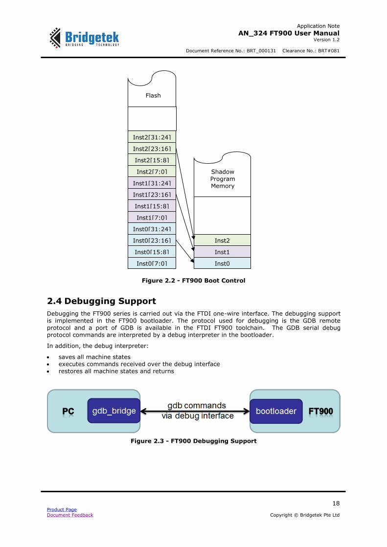
2.3 FT900 Boot Control
Upon reset, boot control takes control of the memory buses and puts the CPU in a reset state.
It automatically transfers the data from the flash memory to the CPU program memory, starting
from address 0 on both sides. Boot control calculates a CRC check over the entire contents of flash (256KB) and the result is placed in CRCH and CRCL registers found in the flash control module.
Application Note
AN_324 FT900 User Manual Version 1.2
Document Reference No.: BRT_000131 Clearance No.: BRT#081
18 Product Page Document Feedback Copyright © Bridgetek Pte Ltd
Figure 2.2 - FT900 Boot Control
2.4 Debugging Support
Debugging the FT900 series is carried out via the FTDI one-wire interface. The debugging support is implemented in the FT900 bootloader. The protocol used for debugging is the GDB remote protocol and a port of GDB is available in the FTDI FT900 toolchain. The GDB serial debug protocol commands are interpreted by a debug interpreter in the bootloader.
In addition, the debug interpreter:
saves all machine states executes commands received over the debug interface restores all machine states and returns
Figure 2.3 - FT900 Debugging Support
Inst0[7:0]
Inst0[15:8]
Inst0[23:16]
Inst0[31:24]
Inst1[7:0]
Inst1[15:8]
Inst1[23:16]
Inst1[31:24]
Inst2[7:0]
Inst2[15:8]
Inst2[23:16]
Inst2[31:24]
Flash
Inst0
Inst1
Inst2
Shadow
Program Memory
Application Note
AN_324 FT900 User Manual Version 1.2
Document Reference No.: BRT_000131 Clearance No.: BRT#081
19 Product Page Document Feedback Copyright © Bridgetek Pte Ltd
3 Register Map
This section lists the I/O map for registers / memory in the device. Please note that some peripherals are not available on some models in the FT900 series. The details can be found in the
table below. An (X) indicates that the peripheral exists and a minus (-) indicates that the peripheral is not available. All other peripherals that are not mentioned are available on all models in the series.
CAN Ethernet Camera SD Host I2S
FT900Q/FT900L X X X X X
FT901Q/FT901L - X X X X
FT902Q/FT902L X - X X X
FT903Q/FT903L - - X X X
FT905Q/FT905L X X - - -
FT906Q/FT906L - X - - -
FT907Q/FT907L X - - - -
FT908Q/FT908L - - - - -
Table 3.1 - Peripheral Availability on FT900 Series Models
The register map of the peripherals is as follows:
Function Address Base Range Access Mechanism
General Setup 0x10000 0x100BF DW, W, B
Interrupt
Controller 0x100C0 0x100FF DW, W, B
USB Host 0x10100 0x1017F DW, W, B
USB Host RAM 0x11000 0x12FFF DW, W, B
USB Device 0x10180 0x1021F B
Ethernet 0x10220 0x1023F DW, W, B (DW for FIFO)
CAN 0 0x10240 0x1025F B
CAN 1 0x10260 0x1027F B
RTC 0x10280 0x1029F DW
SPI Master 0x102A0 0x102BF DW
SPI Slave 0 0x102C0 0x102DF DW
SPI Slave 1 0x102E0 0x102FF DW
I2C Master 0x10300 0x1030F B
I2C Slave 0x10310 0x1031F B
UART 0 0x10320 0x1032F B

Application Note
AN_324 FT900 User Manual Version 1.2
Document Reference No.: BRT_000131 Clearance No.: BRT#081
20 Product Page Document Feedback Copyright © Bridgetek Pte Ltd
Function Address Base Range Access Mechanism
UART 1 0x10330 0x1033F B
Timers/Watchdog 0x10340 0x1034F B
I2S (Master/Slave) 0x10350 0x1035F W
Data Capture 0x10360 0x1036F DW
PWM 0x103C0 0x103FF B for registers, W for FIFO
SD Host 0x10400 0x107FF DW
Flash Controller 0x10800 0x108BF B
* DW (Double-Word): 32-bit; W (Word): 16-bit; B (Byte): 8-bit
Table 3.2 - Register Map for FT900 Series
Application Note
AN_324 FT900 User Manual Version 1.2
Document Reference No.: BRT_000131 Clearance No.: BRT#081
21 Product Page Document Feedback Copyright © Bridgetek Pte Ltd
4 Notations
These notations are used in the register descriptions:
Terms Description
Reserved Do not read/write the location
RO Read-only
ROC Read-only / Clear-when-read
RW Read- and Write-able
RW1C Read and Write-1-to-clear
RW1S Read and Write-1-to-set
RWAC Read- and Write-able with automatic clear
W1S Write-1-to-set
W1T Write-1-to-trigger-event
WO Write-only
Table 4.1 - Notations used in Register Description
Application Note
AN_324 FT900 User Manual Version 1.2
Document Reference No.: BRT_000131 Clearance No.: BRT#081
22 Product Page Document Feedback Copyright © Bridgetek Pte Ltd
5 General System Registers
This section describes the registers that govern the general behavior of the FT900.
5.1 Register Summary
Listed below are the registers with their offset from the base address (0x10000). All registers can be accessed via Byte (8-bit), Word (16-bit) or Double-Word (32-bit) mode.
Address Offset
Register
Default value
References
0x00 HIPID - Chip ID Register 0x09XXXXXX Section 5.2.1
0x04 EFCFG - Chip Configuration Register 0xXXXXXXXX Section 5.2.2
0x08 CLKCFG - Clock Configuration Register 0x00000000 Section 5.2.3
0x0C PMCFG - Power Management Register 0x00000000 Section 5.2.4
0x10 PTSTNSET - Test & Set Register 0x00001000 Section 5.2.5
0x14 PTSTNSETR - Test & Set Shadow Register 0x00000000 Section 5.2.6
0x18 MSC0CFG - Miscellaneous Configuration Register 0x00000000 Section 5.2.7
0x1C Pin 00 – 03 Register 0x04080808 Section 5.2.8.1
0x20 Pin 04 – 07 Register 0x04040404 Section 5.2.8.2
0x24 Pin 08 – 11 Register 0x04040404 Section 5.2.8.3
0x28 Pin 12 – 15 Register 0x04040404 Section 5.2.8.4
0x2C Pin 16 – 19 Register 0x04040404 Section 5.2.8.5
0x30 Pin 20 – 23 Register 0x04040404 Section 5.2.8.6
0x34 Pin 24 – 27 Register 0x04040404 Section 5.2.8.7
0x38 Pin 28 – 31 Register 0x04040404 Section 5.2.8.8
0x3C Pin 32 – 35 Register 0x04040404 Section 5.2.8.9
0x40 Pin 36 – 39 Register 0x04040404 Section 5.2.8.10
0x44 Pin 40 – 43 Register 0x04040404 Section 5.2.8.11
0x48 Pin 44 – 47 Register 0x04040404 Section 5.2.8.12
0x4C Pin 48 – 51 Register 0x04040404 Section 5.2.8.13
0x50 Pin 52 – 55 Register 0x04040404 Section 5.2.8.14
0x54 Pin 56 – 59 Register 0x04040404 Section 5.2.8.15
0x58 Pin 60 – 63 Register 0x04040404 Section 5.2.8.16

Application Note
AN_324 FT900 User Manual Version 1.2
Document Reference No.: BRT_000131 Clearance No.: BRT#081
23 Product Page Document Feedback Copyright © Bridgetek Pte Ltd
0x5C Pin 64 – 66 Register 0x04040404 Section 5.2.8.17
0x60 GPIO 00 – 07 Configuration Register 0x00000000 Section 5.2.9.1
0x64 GPIO 08 – 15 Configuration Register 0x00000000 Section 5.2.9.2
0x68 GPIO 16 – 23 Configuration Register 0x00000000 Section 5.2.9.3
0x6C GPIO 24 – 31 Configuration Register 0x00000000 Section 5.2.9.4
0x70 GPIO 32 – 39 Configuration Register 0x00000000 Section 5.2.9.5
0x74 GPIO 40 – 47 Configuration Register 0x00000000 Section 5.2.9.6
0x78 GPIO 48 – 55 Configuration Register 0x00000000 Section 5.2.9.7
0x7C GPIO 56 – 63 Configuration Register 0x00000000 Section 5.2.9.8
0x80 GPIO 64 – 66 Configuration Register 0x00000000 Section 5.2.9.9
0x84 GPIO 00 – 31 Value Register 0x00000000 Section 5.2.10.1
0x88 GPIO 32 – 63 Value Register 0x00000000 Section 5.2.10.2
0x8C GPIO 64 – 66 Value Register 0x00000000 Section 5.2.10.3
0x90 GPIO 00 – 31 Interrupt Enable Register 0x00000000 Section 5.2.11.1
0x94 GPIO 32 – 63 Interrupt Enable Register 0x00000000 Section 5.2.11.2
0x98 GPIO 64 – 66 Interrupt Enable Register 0x00000000 Section 5.2.11.3
0x9C GPIO 00 – 31 Interrupt Pending Register 0x00000000 Section 5.2.12.1
0xA0 GPIO 32 – 63 Interrupt Pending Register 0x00000000 Section 5.2.12.2
0xA4 GPIO 64 – 66 Interrupt Pending Register 0x00000000 Section 5.2.12.3
0xA8 ETH_PHY_CFG - Ethernet PHY Miscellaneous Configuration Register
0x00070300 Section 5.2.13
0xAC ETH_PHY_ID - Ethernet PHY ID Register 0x00000000 Section 5.2.14
0xB0 DAC_ADC_CONF - ADC/DAC Configuration/Status Register
0x00000000 Section 5.2.15
0xB4 DAC_ADC_CNT - ADC/DAC Count Register 0x63000000 Section 5.2.16
0xB8 DAC_ADC_DATA - ADC/DAC Data Register 0x00000000 Section 5.2.17
Table 5.1 - Overview of General System Registers
Application Note
AN_324 FT900 User Manual Version 1.2
Document Reference No.: BRT_000131 Clearance No.: BRT#081
24 Product Page Document Feedback Copyright © Bridgetek Pte Ltd
5.2 Register Details
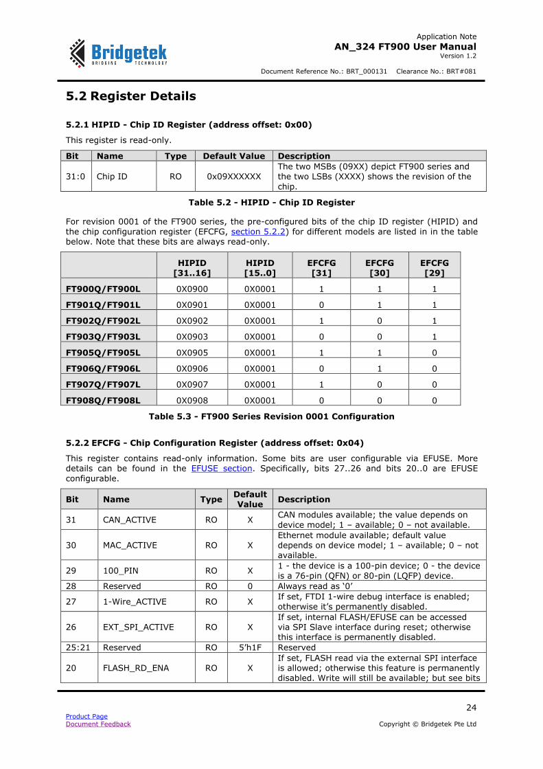
5.2.1 HIPID - Chip ID Register (address offset: 0x00)
This register is read-only.
Bit Name Type Default Value Description
31:0 Chip ID RO 0x09XXXXXX The two MSBs (09XX) depict FT900 series and the two LSBs (XXXX) shows the revision of the
chip.
Table 5.2 - HIPID - Chip ID Register
For revision 0001 of the FT900 series, the pre-configured bits of the chip ID register (HIPID) and
the chip configuration register (EFCFG, section 5.2.2) for different models are listed in in the table below. Note that these bits are always read-only.
HIPID
[31..16] HIPID [15..0]
EFCFG [31]
EFCFG [30]
EFCFG [29]
FT900Q/FT900L 0X0900 0X0001 1 1 1
FT901Q/FT901L 0X0901 0X0001 0 1 1
FT902Q/FT902L 0X0902 0X0001 1 0 1
FT903Q/FT903L 0X0903 0X0001 0 0 1
FT905Q/FT905L 0X0905 0X0001 1 1 0
FT906Q/FT906L 0X0906 0X0001 0 1 0
FT907Q/FT907L 0X0907 0X0001 1 0 0
FT908Q/FT908L 0X0908 0X0001 0 0 0
Table 5.3 - FT900 Series Revision 0001 Configuration
5.2.2 EFCFG - Chip Configuration Register (address offset: 0x04)
This register contains read-only information. Some bits are user configurable via EFUSE. More details can be found in the EFUSE section. Specifically, bits 27..26 and bits 20..0 are EFUSE
configurable.
Bit Name Type Default Value
Description
31 CAN_ACTIVE RO X CAN modules available; the value depends on
device model; 1 – available; 0 – not available.
30 MAC_ACTIVE RO X Ethernet module available; default value depends on device model; 1 – available; 0 – not available.
29 100_PIN RO X 1 - the device is a 100-pin device; 0 - the device is a 76-pin (QFN) or 80-pin (LQFP) device.
28 Reserved RO 0 Always read as ‘0’
27 1-Wire_ACTIVE RO X If set, FTDI 1-wire debug interface is enabled;
otherwise it’s permanently disabled.
26 EXT_SPI_ACTIVE RO X If set, internal FLASH/EFUSE can be accessed via SPI Slave interface during reset; otherwise this interface is permanently disabled.
25:21 Reserved RO 5’h1F Reserved
20 FLASH_RD_ENA RO X If set, FLASH read via the external SPI interface is allowed; otherwise this feature is permanently disabled. Write will still be available; but see bits
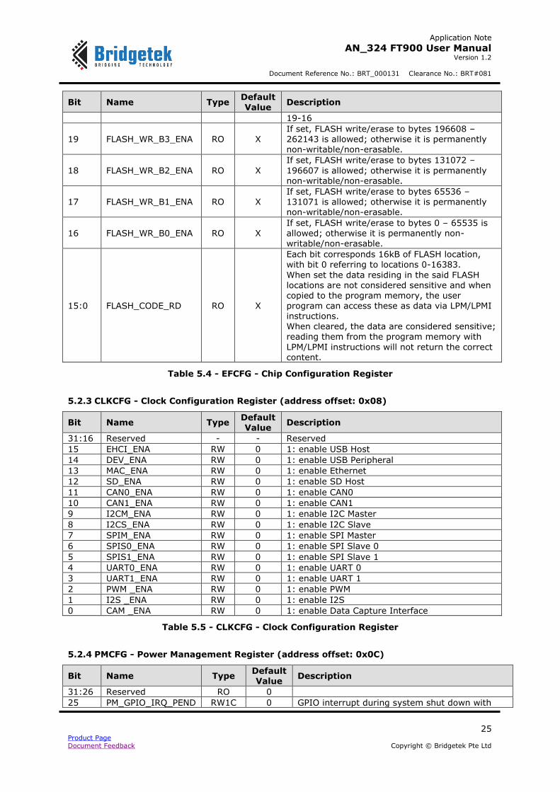
Application Note
AN_324 FT900 User Manual Version 1.2
Document Reference No.: BRT_000131 Clearance No.: BRT#081
25 Product Page Document Feedback Copyright © Bridgetek Pte Ltd
Bit Name Type Default Value
Description
19-16
19 FLASH_WR_B3_ENA RO X If set, FLASH write/erase to bytes 196608 – 262143 is allowed; otherwise it is permanently non-writable/non-erasable.
18 FLASH_WR_B2_ENA RO X
If set, FLASH write/erase to bytes 131072 –
196607 is allowed; otherwise it is permanently non-writable/non-erasable.
17 FLASH_WR_B1_ENA RO X If set, FLASH write/erase to bytes 65536 – 131071 is allowed; otherwise it is permanently non-writable/non-erasable.
16 FLASH_WR_B0_ENA RO X If set, FLASH write/erase to bytes 0 – 65535 is allowed; otherwise it is permanently non-writable/non-erasable.
15:0 FLASH_CODE_RD RO X
Each bit corresponds 16kB of FLASH location,
with bit 0 referring to locations 0-16383.
When set the data residing in the said FLASH locations are not considered sensitive and when copied to the program memory, the user program can access these as data via LPM/LPMI instructions. When cleared, the data are considered sensitive; reading them from the program memory with
LPM/LPMI instructions will not return the correct content.
Table 5.4 - EFCFG - Chip Configuration Register
5.2.3 CLKCFG - Clock Configuration Register (address offset: 0x08)
Bit Name Type Default Value
Description
31:16 Reserved - - Reserved
15 EHCI_ENA RW 0 1: enable USB Host
14 DEV_ENA RW 0 1: enable USB Peripheral
13 MAC_ENA RW 0 1: enable Ethernet
12 SD_ENA RW 0 1: enable SD Host
11 CAN0_ENA RW 0 1: enable CAN0
10 CAN1_ENA RW 0 1: enable CAN1
9 I2CM_ENA RW 0 1: enable I2C Master
8 I2CS_ENA RW 0 1: enable I2C Slave
7 SPIM_ENA RW 0 1: enable SPI Master
6 SPIS0_ENA RW 0 1: enable SPI Slave 0
5 SPIS1_ENA RW 0 1: enable SPI Slave 1
4 UART0_ENA RW 0 1: enable UART 0
3 UART1_ENA RW 0 1: enable UART 1
2 PWM _ENA RW 0 1: enable PWM
1 I2S _ENA RW 0 1: enable I2S
0 CAM _ENA RW 0 1: enable Data Capture Interface
Table 5.5 - CLKCFG - Clock Configuration Register
5.2.4 PMCFG - Power Management Register (address offset: 0x0C)
Bit Name Type Default Value
Description
31:26 Reserved RO 0
25 PM_GPIO_IRQ_PEND RW1C 0 GPIO interrupt during system shut down with
Application Note
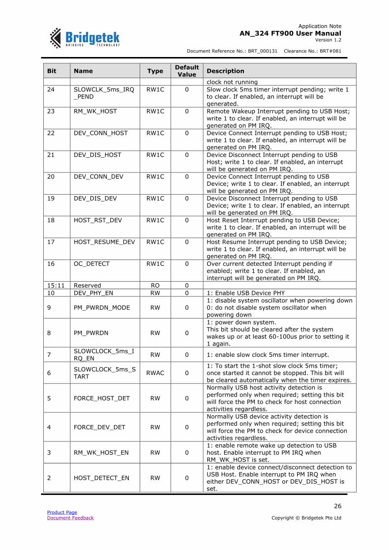
AN_324 FT900 User Manual Version 1.2
Document Reference No.: BRT_000131 Clearance No.: BRT#081
26 Product Page Document Feedback Copyright © Bridgetek Pte Ltd
Bit Name Type Default Value
Description
clock not running
24 SLOWCLK_5ms_IRQ_PEND
RW1C 0 Slow clock 5ms timer interrupt pending; write 1 to clear. If enabled, an interrupt will be generated.
23 RM_WK_HOST RW1C 0 Remote Wakeup Interrupt pending to USB Host;
write 1 to clear. If enabled, an interrupt will be generated on PM IRQ.
22 DEV_CONN_HOST RW1C 0 Device Connect Interrupt pending to USB Host; write 1 to clear. If enabled, an interrupt will be generated on PM IRQ.
21 DEV_DIS_HOST RW1C 0 Device Disconnect Interrupt pending to USB Host; write 1 to clear. If enabled, an interrupt will be generated on PM IRQ.
20 DEV_CONN_DEV RW1C 0 Device Connect Interrupt pending to USB
Device; write 1 to clear. If enabled, an interrupt
will be generated on PM IRQ.
19 DEV_DIS_DEV RW1C 0 Device Disconnect Interrupt pending to USB Device; write 1 to clear. If enabled, an interrupt will be generated on PM IRQ.
18 HOST_RST_DEV RW1C 0 Host Reset Interrupt pending to USB Device; write 1 to clear. If enabled, an interrupt will be generated on PM IRQ.
17 HOST_RESUME_DEV RW1C 0 Host Resume Interrupt pending to USB Device; write 1 to clear. If enabled, an interrupt will be generated on PM IRQ.
16 OC_DETECT RW1C 0 Over current detected Interrupt pending if enabled; write 1 to clear. If enabled, an interrupt will be generated on PM IRQ.
15:11 Reserved RO 0
10 DEV_PHY_EN RW 0 1: Enable USB Device PHY
9 PM_PWRDN_MODE RW 0
1: disable system oscillator when powering down
0: do not disable system oscillator when powering down
8 PM_PWRDN RW 0
1: power down system. This bit should be cleared after the system wakes up or at least 60-100us prior to setting it 1 again.
7 SLOWCLOCK_5ms_I
RQ_EN RW 0 1: enable slow clock 5ms timer interrupt.
6 SLOWCLOCK_5ms_S
TART RWAC 0
1: To start the 1-shot slow clock 5ms timer; once started it cannot be stopped. This bit will be cleared automatically when the timer expires.
5 FORCE_HOST_DET RW 0
Normally USB host activity detection is
performed only when required; setting this bit will force the PM to check for host connection activities regardless.
4 FORCE_DEV_DET RW 0
Normally USB device activity detection is performed only when required; setting this bit
will force the PM to check for device connection activities regardless.
3 RM_WK_HOST_EN RW 0 1: enable remote wake up detection to USB host. Enable interrupt to PM IRQ when RM_WK_HOST is set.
2 HOST_DETECT_EN RW 0
1: enable device connect/disconnect detection to USB Host. Enable interrupt to PM IRQ when either DEV_CONN_HOST or DEV_DIS_HOST is set.
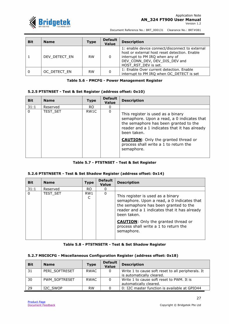
Application Note
AN_324 FT900 User Manual Version 1.2
Document Reference No.: BRT_000131 Clearance No.: BRT#081
27 Product Page Document Feedback Copyright © Bridgetek Pte Ltd
Bit Name Type Default Value
Description
1 DEV_DETECT_EN RW 0
1: enable device connect/disconnect to external host or external host reset detection. Enable interrupt to PM IRQ when any of DEV_CONN_DEV, DEV_DIS_DEV and HOST_RST_DEV is set.
0 OC_DETECT_EN RW 0 1: Enable Over current detection. Enable
interrupt to PM IRQ when OC_DETECT is set
Table 5.6 - PMCFG - Power Management Register
5.2.5 PTSTNSET - Test & Set Register (address offset: 0x10)
Bit Name Type Default
Value Description
31:1 Reserved RO 0
0 TEST_SET RW1C 0 This register is used as a binary
semaphore. Upon a read, a 0 indicates that
the semaphore has been granted to the
reader and a 1 indicates that it has already
been taken.
CAUTION: Only the granted thread or
process shall write a 1 to return the
semaphore.
Table 5.7 - PTSTNSET - Test & Set Register
5.2.6 PTSTNSETR - Test & Set Shadow Register (address offset: 0x14)
Bit Name Type Default Value
Description
31:1 Reserved RO 0
0 TEST_SET RW1C
0 This register is used as a binary
semaphore. Upon a read, a 0 indicates that
the semaphore has been granted to the
reader and a 1 indicates that it has already
been taken.
CAUTION: Only the granted thread or
process shall write a 1 to return the
semaphore.
Table 5.8 - PTSTNSETR - Test & Set Shadow Register
5.2.7 MSC0CFG - Miscellaneous Configuration Register (address offset: 0x18)
Bit Name Type Default Value
Description
31 PERI_SOFTRESET RWAC 0 Write 1 to cause soft reset to all peripherals. It
is automatically cleared.
30 PWM_SOFTRESET RWAC 0 Write 1 to cause soft reset to PWM. It is automatically cleared.
29 I2C_SWOP RW 0 0: I2C master function is available at GPIO44
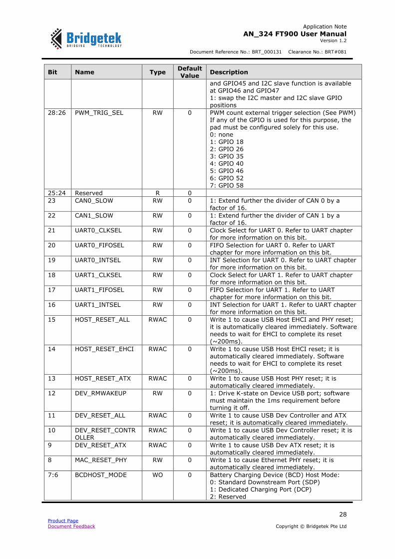
Application Note
AN_324 FT900 User Manual Version 1.2
Document Reference No.: BRT_000131 Clearance No.: BRT#081
28 Product Page Document Feedback Copyright © Bridgetek Pte Ltd
Bit Name Type Default Value
Description
and GPIO45 and I2C slave function is available at GPIO46 and GPIO47 1: swap the I2C master and I2C slave GPIO positions
28:26 PWM_TRIG_SEL RW 0 PWM count external trigger selection (See PWM) If any of the GPIO is used for this purpose, the
pad must be configured solely for this use. 0: none 1: GPIO 18 2: GPIO 26 3: GPIO 35 4: GPIO 40 5: GPIO 46
6: GPIO 52
7: GPIO 58
25:24 Reserved R 0
23 CAN0_SLOW RW 0 1: Extend further the divider of CAN 0 by a
factor of 16.
22 CAN1_SLOW RW 0 1: Extend further the divider of CAN 1 by a factor of 16.
21 UART0_CLKSEL RW 0 Clock Select for UART 0. Refer to UART chapter for more information on this bit.
20 UART0_FIFOSEL RW 0 FIFO Selection for UART 0. Refer to UART chapter for more information on this bit.
19 UART0_INTSEL RW 0 INT Selection for UART 0. Refer to UART chapter for more information on this bit.
18 UART1_CLKSEL RW 0 Clock Select for UART 1. Refer to UART chapter for more information on this bit.
17 UART1_FIFOSEL RW 0 FIFO Selection for UART 1. Refer to UART chapter for more information on this bit.
16 UART1_INTSEL RW 0 INT Selection for UART 1. Refer to UART chapter
for more information on this bit.
15 HOST_RESET_ALL RWAC 0 Write 1 to cause USB Host EHCI and PHY reset; it is automatically cleared immediately. Software needs to wait for EHCI to complete its reset
(~200ms).
14 HOST_RESET_EHCI RWAC 0 Write 1 to cause USB Host EHCI reset; it is automatically cleared immediately. Software needs to wait for EHCI to complete its reset (~200ms).
13 HOST_RESET_ATX RWAC 0 Write 1 to cause USB Host PHY reset; it is automatically cleared immediately.
12 DEV_RMWAKEUP RW 0 1: Drive K-state on Device USB port; software must maintain the 1ms requirement before turning it off.
11 DEV_RESET_ALL RWAC 0 Write 1 to cause USB Dev Controller and ATX reset; it is automatically cleared immediately.
10 DEV_RESET_CONTR
OLLER
RWAC 0 Write 1 to cause USB Dev Controller reset; it is
automatically cleared immediately.
9 DEV_RESET_ATX RWAC 0 Write 1 to cause USB Dev ATX reset; it is automatically cleared immediately.
8 MAC_RESET_PHY RW 0 Write 1 to cause Ethernet PHY reset; it is automatically cleared immediately.
7:6 BCDHOST_MODE WO 0 Battery Charging Device (BCD) Host Mode: 0: Standard Downstream Port (SDP) 1: Dedicated Charging Port (DCP) 2: Reserved
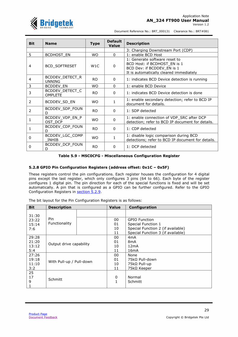
Application Note
AN_324 FT900 User Manual Version 1.2
Document Reference No.: BRT_000131 Clearance No.: BRT#081
29 Product Page Document Feedback Copyright © Bridgetek Pte Ltd
Bit Name Type Default Value
Description
3: Charging Downstream Port (CDP)
5 BCDHOST_EN WO 0 1: enable BCD Host
4 BCD_SOFTRESET W1C 0
1: Generate software reset to BCD Host: if BCDHOST_EN is 1 BCD Dev: if BCDDEV_EN is 1
It is automatically cleared immediately
4 BCDDEV_DETECT_RUNNING
RO 0 1: indicates BCD Device detection is running
3 BCDDEV_EN WO 0 1: enable BCD Device
3 BCDDEV_DETECT_COMPLETE
RO 0 1: indicates BCD Device detection is done
2 BCDDEV_SD_EN WO 1 1: enable secondary detection; refer to BCD IP document for details.
2 BCDDEV_SDP_FOUN
D RO 0 1: SDP detected
1 BCDDEV_VDP_EN_POST_DCP
WO 0 1: enable connection of VDP_SRC after DCP detection; refer to BCD IP document for details.
1 BCDDEV_CDP_FOUND
RO 0 1: CDP detected
0 BCDDEV_LGC_COMP_INHIB
WO 1 1: disable logic comparison during BCD detections; refer to BCD IP document for details.
0 BCDDEV_DCP_FOUN
D RO 0 1: DCP detected
Table 5.9 - MSC0CFG - Miscellaneous Configuration Register
5.2.8 GPIO Pin Configuration Registers (address offset: 0x1C – 0x5F)
These registers control the pin configurations. Each register houses the configuration for 4 digital pins except the last register, which only configures 3 pins (64 to 66). Each byte of the register
configures 1 digital pin. The pin direction for each of the special functions is fixed and will be set
automatically. A pin that is configured as a GPIO can be further configured. Refer to the GPIO Configuration Registers in section 5.2.9. The bit layout for the Pin Configuration Registers is as follows:
Bit Description Value Configuration
31:30 23:22 15:14
7:6
Pin Functionality
00 01 10 11
GPIO Function Special Function 1 Special Function 2 (if available) Special Function 3 (if available)
29:28 21:20 13:12 5:4
Output drive capability
00 01 10 11
4mA 8mA 12mA 16mA
27:26 19:18
11:10 3:2
With Pull-up / Pull-down
00 01
10 11
None 75kΩ Pull-down
75kΩ Pull-up 75kΩ Keeper
25 17
9 1
Schmitt 0
1
Normal
Schmitt

Application Note
AN_324 FT900 User Manual Version 1.2
Document Reference No.: BRT_000131 Clearance No.: BRT#081
30 Product Page Document Feedback Copyright © Bridgetek Pte Ltd
24 16 8 0
Slew Rate 0 1
Fast Slow
Table 5.10 - Pin Configuration Register Description
The following tables give more details about each Pin Configuration Register. The “Pin Functionality Bits” section refers to bits 31:30, 23:22, 15:14, 7:6 in each register for configuring the
corresponding pin to perform a specific functionality. Refer to table 5.10 above.
5.2.8.1 Pin 00 – 03 Register (address offset: 0x1C)
Bit Name Type Default Value
Pin Functionality Bits
00 01 10 11
31:24 PIN03_CFG RW 8’h04 GPIO 3 VBUS Detect
- -
23:16 PIN02_CFG RW 8’h08 GPIO 2 - - -
15:8 PIN01_CFG RW 8’h08 GPIO 1 OCN - -
7:0 PIN00_CFG RW 8’h08 GPIO 0 - - -
Table 5.11 - Pin 00 – 03 Register
5.2.8.2 Pin 04 – 07 Register (address offset: 0x20)
Bit Name Type Default Value
Pin Functionality Bits
00 01 10 11
31:24 PIN07_CFG RW 8’h04 GPIO 7 Cam Pclk - ADC Ch2
23:16 PIN06_CFG RW 8’h04 GPIO 6 Cam Ext Clk
- ADC Ch1
15:8 PIN05_CFG RW 8’h04 GPIO 5 Ethernet LED 1
- -
7:0 PIN04_CFG RW 8’h04 GPIO 4 Ethernet
LED 0
-
Table 5.12 - Pin 04 – 07 Register
5.2.8.3 Pin 08 – 11 Register (address offset: 0x24)
Bit Name Type Default Value
Pin Functionality Bits
00 01 10 11
31:24 PIN11_CFG RW 8’h04 GPIO 11 Cam D6 - ADC Ch6
23:16 PIN10_CFG RW 8’h04 GPIO 10 Cam D7 - ADC Ch5
15:8 PIN09_CFG RW 8’h04 GPIO 9 Cam HD - ADC Ch4
7:0 PIN08_CFG RW 8’h04 GPIO 8 Cam VD - ADC Ch3
Table 5.13 - Pin 08 – 11 Register
5.2.8.4 Pin 12 – 15 Register (address offset: 0x28)
Bit Name Type Default
Value
Pin Functionality Bits
00 01 10 11
31:24 PIN15_CFG RW 8’h04 GPIO 15 Cam D2 CAN 0 Tx -
23:16 PIN14_CFG RW 8’h04 GPIO 14 Cam D3 - DAC Ch0
15:8 PIN13_CFG RW 8’h04 GPIO 13 Cam D4 - DAC Ch1
7:0 PIN12_CFG RW 8’h04 GPIO 12 Cam D5 - ADC Ch7
Table 5.14 - Pin 12 – 15 Register
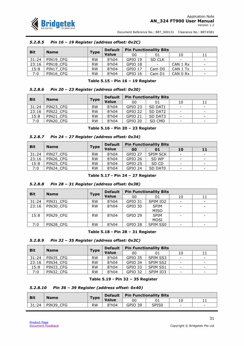
Application Note
AN_324 FT900 User Manual Version 1.2
Document Reference No.: BRT_000131 Clearance No.: BRT#081
31 Product Page Document Feedback Copyright © Bridgetek Pte Ltd
5.2.8.5 Pin 16 – 19 Register (address offset: 0x2C)
Bit Name Type Default Value
Pin Functionality Bits
00 01 10 11
31:24 PIN19_CFG RW 8’h04 GPIO 19 SD CLK - -
23:16 PIN18_CFG RW 8’h04 GPIO 18 - CAN 1 Rx -
15:8 PIN17_CFG RW 8’h04 GPIO 17 Cam D0 CAN 1 Tx -
7:0 PIN16_CFG RW 8’h04 GPIO 16 Cam D1 CAN 0 Rx -
Table 5.15 - Pin 16 – 19 Register
5.2.8.6 Pin 20 – 23 Register (address offset: 0x30)
Bit Name Type Default Value
Pin Functionality Bits
00 01 10 11
31:24 PIN23_CFG RW 8’h04 GPIO 23 SD DAT1 - -
23:16 PIN22_CFG RW 8’h04 GPIO 22 SD DAT2 - -
15:8 PIN21_CFG RW 8’h04 GPIO 21 SD DAT3 - -
7:0 PIN20_CFG RW 8’h04 GPIO 20 SD CMD - -
Table 5.16 - Pin 20 – 23 Register
5.2.8.7 Pin 24 – 27 Register (address offset: 0x34)
Bit Name Type Default Value
Pin Functionality Bits
00 01 10 11
31:24 PIN27_CFG RW 8’h04 GPIO 27 SPIM SCK - -
23:16 PIN26_CFG RW 8’h04 GPIO 26 SD WP - -
15:8 PIN25_CFG RW 8’h04 GPIO 25 SD CD - -
7:0 PIN24_CFG RW 8’h04 GPIO 24 SD DAT0 - -
Table 5.17 - Pin 24 – 27 Register
5.2.8.8 Pin 28 – 31 Register (address offset: 0x38)
Bit Name Type Default
Value
Pin Functionality Bits
00 01 10 11
31:24 PIN31_CFG RW 8’h04 GPIO 31 SPIM IO2 - -
23:16 PIN30_CFG RW 8’h04 GPIO 30 SPIM MISO
- -
15:8 PIN29_CFG RW 8’h04 GPIO 29 SPIM MOSI
- -
7:0 PIN28_CFG RW 8’h04 GPIO 28 SPIM SS0 - -
Table 5.18 - Pin 28 – 31 Register
5.2.8.9 Pin 32 – 35 Register (address offset: 0x3C)
Bit Name Type Default Value
Pin Functionality Bits
00 01 10 11
31:24 PIN35_CFG RW 8’h04 GPIO 35 SPIM SS3 - -
23:16 PIN34_CFG RW 8’h04 GPIO 34 SPIM SS2 - -
15:8 PIN33_CFG RW 8’h04 GPIO 33 SPIM SS1 - -
7:0 PIN32_CFG RW 8’h04 GPIO 32 SPIM IO3 - -
Table 5.19 - Pin 32 – 35 Register
5.2.8.10 Pin 36 – 39 Register (address offset: 0x40)
Bit Name Type Default Value
Pin Functionality Bits
00 01 10 11
31:24 PIN39_CFG RW 8’h04 GPIO 39 SPIS0 - -
Application Note
AN_324 FT900 User Manual Version 1.2
Document Reference No.: BRT_000131 Clearance No.: BRT#081
32 Product Page Document Feedback Copyright © Bridgetek Pte Ltd
MISO
23:16 PIN38_CFG RW 8’h04 GPIO 38 SPIS0
MOSI
- -
15:8 PIN37_CFG RW 8’h04 GPIO 37 SPIS0 SS - -
7:0 PIN36_CFG RW 8’h04 GPIO 36 SPIS0 SCK
- -
Table 5.20 - Pin 36 – 39 Register
5.2.8.11 Pin 40 – 43 Register (address offset: 0x44)
Bit Name Type Default Value
Pin Functionality Bits
00 01 10 11
31:24 PIN43_CFG RW 8’h04 GPIO 43 SPIS1 MISO
- -
23:16 PIN42_CFG RW 8’h04 GPIO 42 SPIS1 MOSI
- -
15:8 PIN41_CFG RW 8’h04 GPIO 41 SPIS1 SS - -
7:0 PIN40_CFG RW 8’h04 GPIO 40 SPIS1 SCK
- -
Table 5.21 - Pin 40 – 43 Register
5.2.8.12 Pin 44 – 47 Register (address offset: 0x48)
Bit Name Type Default Value
Pin Functionality Bits (note that I2C Master &
Slave pads can be swopped)
00 01 10 11
31:24 PIN47_CFG RW 8’h04 GPIO 47 I2C1 SDA - -
23:16 PIN46_CFG RW 8’h04 GPIO 46 I2C1 SCL - -
15:8 PIN45_CFG RW 8’h04 GPIO 45 I2C0 SDA - -
7:0 PIN44_CFG RW 8’h04 GPIO 44 I2C0 SCL - -
Table 5.22 - Pin 44 – 47 Register
5.2.8.13 Pin 48 – 51 Register (address offset: 0x4C)
Bit Name Type Default Value
Pin Functionality Bits
00 01 10 11
31:24 PIN51_CFG RW 8’h04 GPIO 51 - - UART0 CTS
23:16 PIN50_CFG RW 8’h04 GPIO 50 - - UART0 RTS
15:8 PIN49_CFG RW 8’h04 GPIO 49 - - UART0 RXD
7:0 PIN48_CFG RW 8’h04 GPIO 48 - - UART0 TXD
Table 5.23 - Pin 48 – 51 Register
5.2.8.14 Pin 52 – 55 Register (address offset: 0x50)
Bit Name Type Default Value
Pin Functionality Bits
00 01 10 11
31:24 PIN55_CFG RW 8’h04 GPIO 55 PWM Ch7 UART1 CTS
UART0 RI
23:16 PIN54_CFG RW 8’h04 GPIO 54 PWM Ch6 UART1 RTS
UART0 DCD
15:8 PIN53_CFG RW 8’h04 GPIO 53 PWM Ch5 UART1 RXD
UART0 DSR
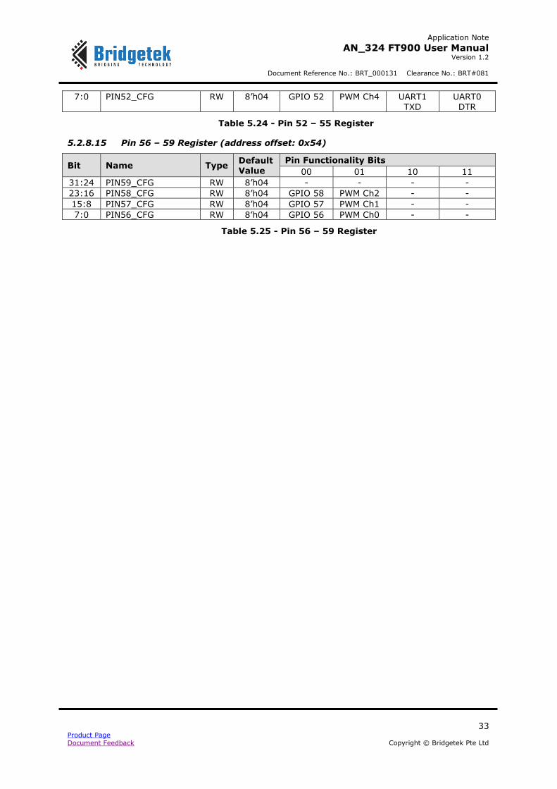
Application Note
AN_324 FT900 User Manual Version 1.2
Document Reference No.: BRT_000131 Clearance No.: BRT#081
33 Product Page Document Feedback Copyright © Bridgetek Pte Ltd
7:0 PIN52_CFG RW 8’h04 GPIO 52 PWM Ch4 UART1 TXD
UART0 DTR
Table 5.24 - Pin 52 – 55 Register
5.2.8.15 Pin 56 – 59 Register (address offset: 0x54)
Bit Name Type Default Value
Pin Functionality Bits
00 01 10 11
31:24 PIN59_CFG RW 8’h04 - - - -
23:16 PIN58_CFG RW 8’h04 GPIO 58 PWM Ch2 - -
15:8 PIN57_CFG RW 8’h04 GPIO 57 PWM Ch1 - -
7:0 PIN56_CFG RW 8’h04 GPIO 56 PWM Ch0 - -
Table 5.25 - Pin 56 – 59 Register

Application Note
AN_324 FT900 User Manual Version 1.2
Document Reference No.: BRT_000131 Clearance No.: BRT#081
34 Product Page Document Feedback Copyright © Bridgetek Pte Ltd
5.2.8.16 Pin 60 – 63 Register (address offset: 0x58)
Bit Name Type Default Value
Pin Functionality Bits
00 01 10 11
31:24 PIN63_CFG RW 8’h04 GPIO 63 I2SM LRCLK
I2SS LRCLK
-
23:16 PIN62_CFG RW 8’h04 GPIO 62 I2SM BCLK
I2SS BCLK
-
15:8 PIN61_CFG RW 8’h04 GPIO 61 I2S SDAI - -
7:0 PIN60_CFG RW 8’h04 GPIO 60 I2S SDAO - -
Table 5.26 - Pin 60 – 63 Register
5.2.8.17 Pin 64 – 66 Register (address offset: 0x5C)
Bit Name Type Default
Value
Pin Functionality Bits
00 01 10 11
31:24 Reserved RW 8’h04 - - - -
23:16 PIN66_CFG RW 8’h04 GPIO 66 I2SM CLK24
- -
15:8 PIN65_CFG RW 8’h04 GPIO 65 I2SM CLK22
- -
7:0 PIN64_CFG RW 8’h04 GPIO 64 I2S MCLK - -
Table 5.27 - Pin 64 – 66 Register
5.2.9 GPIO Configuration Registers (address offset: 0x60 – 0x83)
These registers control the GPIO configurations. Each register houses the configuration for 8 digital pads except the last register, which only configures 3 pads (64 to 66). Each nibble of the register
configures 1 digital pad. All GPIOs can function as an interrupt. The polarity can be either positive edge or negative edge if its interrupt capability is enabled. If this feature is desired, the pad must be configured as a GPIO input. Otherwise unpredictable behavior may result.
There is no de-bouncing for all GPIO’s. If they are used as general inputs, and de-
bouncing is needed, then software must handle this. If it’s to be used as an interrupt, the external interrupt source should be glitch free. The bit layout for the GPIO Configuration Registers is as follows:
Bit Description Value Configuration
31:30 27:26
23:22 19:18 15:14 11:10 7:6 3:2
GPIO Direction 00 01 1X
Input Output OD Output
29
25 21 17 13 9 5
1
Interrupt Capable (Also see section 5.2.11, “GPIO Interrupt Enable Registers”)
0 1
No Yes

Application Note
AN_324 FT900 User Manual Version 1.2
Document Reference No.: BRT_000131 Clearance No.: BRT#081
35 Product Page Document Feedback Copyright © Bridgetek Pte Ltd
Bit Description Value Configuration
28
24 20 16 12 8 4 0
Interrupt Edge (only if Interrupt Capable bit is
1)
0 1
Falling Edge Rising Edge
Table 5.28 - GPIO Configuration Register Description
The following tables give more details about which bits control a specific GPIO Pin using the values from Table 5.28.
5.2.9.1 GPIO 00 – 07 Configuration Register (address offset: 0x60)
Bit Name Type Default Value
Description
31:28 GPIO07_CFG RW 0 For GPIO 7
27:24 GPIO06_CFG RW 0 For GPIO 6
23:20 GPIO05_CFG RW 0 For GPIO 5
19:16 GPIO04_CFG RW 0 For GPIO 4
15:12 GPIO03_CFG RW 0 For GPIO 3
11:8 GPIO02_CFG RW 0 For GPIO 2
7:4 GPIO01_CFG RW 0 For GPIO 1
3:0 GPIO00_CFG RW 0 For GPIO 0
Table 5.29 - GPIO 00 – 07 Configuration Register
5.2.9.2 GPIO 08 – 15 Configuration Register (address offset: 0x64)
Bit Name Type Default Value
Description
31:28 GPIO15_CFG RW 0 For GPIO 15
27:24 GPIO14_CFG RW 0 For GPIO 14
23:20 GPIO13_CFG RW 0 For GPIO 13
19:16 GPIO12_CFG RW 0 For GPIO 12
15:12 GPIO11_CFG RW 0 For GPIO 11
11:8 GPIO10_CFG RW 0 For GPIO 10
7:4 GPIO09_CFG RW 0 For GPIO 9
3:0 GPIO08_CFG RW 0 For GPIO 8
Table 5.30 - GPIO 08 – 15 Configuration Register
5.2.9.3 GPIO 16 – 23 Configuration Register (address offset: 0x68)
Bit Name Type Default Value
Description
31:28 GPIO23_CFG RW 0 For GPIO 23
27:24 GPIO22_CFG RW 0 For GPIO 22
23:20 GPIO21_CFG RW 0 For GPIO 21
19:16 GPIO20_CFG RW 0 For GPIO 20
15:12 GPIO19_CFG RW 0 For GPIO 19
11:8 GPIO18_CFG RW 0 For GPIO 18
7:4 GPIO17_CFG RW 0 For GPIO 17
3:0 GPIO16_CFG RW 0 For GPIO 16
Table 5.31 - GPIO 16 – 23 Configuration Register
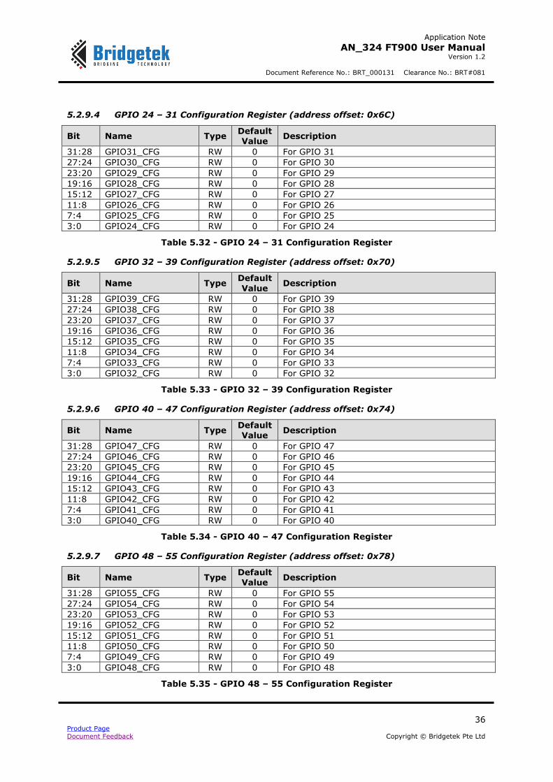
Application Note
AN_324 FT900 User Manual Version 1.2
Document Reference No.: BRT_000131 Clearance No.: BRT#081
36 Product Page Document Feedback Copyright © Bridgetek Pte Ltd
5.2.9.4 GPIO 24 – 31 Configuration Register (address offset: 0x6C)
Bit Name Type Default Value
Description
31:28 GPIO31_CFG RW 0 For GPIO 31
27:24 GPIO30_CFG RW 0 For GPIO 30
23:20 GPIO29_CFG RW 0 For GPIO 29
19:16 GPIO28_CFG RW 0 For GPIO 28
15:12 GPIO27_CFG RW 0 For GPIO 27
11:8 GPIO26_CFG RW 0 For GPIO 26
7:4 GPIO25_CFG RW 0 For GPIO 25
3:0 GPIO24_CFG RW 0 For GPIO 24
Table 5.32 - GPIO 24 – 31 Configuration Register
5.2.9.5 GPIO 32 – 39 Configuration Register (address offset: 0x70)
Bit Name Type Default
Value Description
31:28 GPIO39_CFG RW 0 For GPIO 39
27:24 GPIO38_CFG RW 0 For GPIO 38
23:20 GPIO37_CFG RW 0 For GPIO 37
19:16 GPIO36_CFG RW 0 For GPIO 36
15:12 GPIO35_CFG RW 0 For GPIO 35
11:8 GPIO34_CFG RW 0 For GPIO 34
7:4 GPIO33_CFG RW 0 For GPIO 33
3:0 GPIO32_CFG RW 0 For GPIO 32
Table 5.33 - GPIO 32 – 39 Configuration Register
5.2.9.6 GPIO 40 – 47 Configuration Register (address offset: 0x74)
Bit Name Type Default
Value Description
31:28 GPIO47_CFG RW 0 For GPIO 47
27:24 GPIO46_CFG RW 0 For GPIO 46
23:20 GPIO45_CFG RW 0 For GPIO 45
19:16 GPIO44_CFG RW 0 For GPIO 44
15:12 GPIO43_CFG RW 0 For GPIO 43
11:8 GPIO42_CFG RW 0 For GPIO 42
7:4 GPIO41_CFG RW 0 For GPIO 41
3:0 GPIO40_CFG RW 0 For GPIO 40
Table 5.34 - GPIO 40 – 47 Configuration Register
5.2.9.7 GPIO 48 – 55 Configuration Register (address offset: 0x78)
Bit Name Type Default Value
Description
31:28 GPIO55_CFG RW 0 For GPIO 55
27:24 GPIO54_CFG RW 0 For GPIO 54
23:20 GPIO53_CFG RW 0 For GPIO 53
19:16 GPIO52_CFG RW 0 For GPIO 52
15:12 GPIO51_CFG RW 0 For GPIO 51
11:8 GPIO50_CFG RW 0 For GPIO 50
7:4 GPIO49_CFG RW 0 For GPIO 49
3:0 GPIO48_CFG RW 0 For GPIO 48
Table 5.35 - GPIO 48 – 55 Configuration Register

Application Note
AN_324 FT900 User Manual Version 1.2
Document Reference No.: BRT_000131 Clearance No.: BRT#081
37 Product Page Document Feedback Copyright © Bridgetek Pte Ltd
5.2.9.8 GPIO 56 – 63 Configuration Register (address offset: 0x7C)
Bit Name Type Default Value
Description
31:28 GPIO63_CFG RW 0 For GPIO 63
27:24 GPIO62_CFG RW 0 For GPIO 62
23:20 GPIO61_CFG RW 0 For GPIO 61
19:16 GPIO60_CFG RW 0 For GPIO 60
15:12 GPIO59_CFG RW 0 For GPIO 59
11:8 GPIO58_CFG RW 0 For GPIO 58
7:4 GPIO57_CFG RW 0 For GPIO 57
3:0 GPIO56_CFG RW 0 For GPIO 56
Table 5.36 - GPIO 56 – 63 Configuration Register
5.2.9.9 GPIO 64 – 66 Configuration Register (address offset: 0x80)
Bit Name Type Default
Value Description
31:12 Reserved - - -
11:8 GPIO66_CFG RW 0 For GPIO 66
7:4 GPIO65_CFG RW 0 For GPIO 65
3:0 GPIO64_CFG RW 0 For GPIO 64
Table 5.37 - GPIO 64 – 66 Configuration Register
5.2.10 GPIO Value Registers (address offset: 0x84 – 0x8F)
These registers contain the values for the GPIO pins. Each register contains the value of 32 digital pins except the last register, which only contains the value of 3 pins (64 to 66). Each bit of the register maps to the corresponding digital pin.
5.2.10.1 GPIO 00 – 31 Value Register (address offset: 0x84)
Bit Name Type Default Value
Description
31:0 GPIO_VAL_IN[31:0] RO X Input values of GPIO 31 – 0
31:0 GPIO_VAL_OUT[31:0] WO 0 Output values of GPIO 31 – 0
Table 5.38 - GPIO 00 – 31 Value Register
5.2.10.2 GPIO 32 – 63 Value Register (address offset: 0x88)
Bit Name Type Default Value
Description
31:0 GPIO_VAL_IN[63:32] RO X Input values of GPIO 63 – 32
31:0 GPIO_VAL_OUT[63:32] WO 0 Output values of GPIO 63 - 32
Table 5.39 - GPIO 32 – 63 Value Register
5.2.10.3 GPIO 64 – 66 Value Register (address offset: 0x8C)
Bit Name Type Default
Value Description
31:3 Reserved - - -
2:0 GPIO_VAL_IN[66:64] RO X Input values of GPIO 66 – 64
2:0 GPIO_VAL_OUT[66:64] WO 0 Output values of GPIO 66 - 64
Table 5.40 - GPIO 64 – 66 Value Register

Application Note
AN_324 FT900 User Manual Version 1.2
Document Reference No.: BRT_000131 Clearance No.: BRT#081
38 Product Page Document Feedback Copyright © Bridgetek Pte Ltd
5.2.11 GPIO Interrupt Enable Registers (address offset: 0x90 – 0x9B)
When a pin has been configured as an input with interrupt capability, the GPIO Interrupt Enable Register can be used to enable interrupt generation. Each register enables interrupt generation for 32 digital pins except the last register, which only enables interrupt generation for 3 pins (64 to 66). Each bit of the register enables interrupt generation for 1 digital pin.
These should be used only for pads that have been properly configured as interrupt enabled GPIO inputs.
5.2.11.1 GPIO 00 – 31 Interrupt Enable Register (address offset: 0x90)
Bit Name Type Default Value
Description
31:0 GPIO_INT_EN[31:0] RW 0 GPIO input 31-0 interrupt enable when set.
Table 5.41 - GPIO 00 – 31 Interrupt Enable Register
5.2.11.2 GPIO 32 – 63 Interrupt Enable Register (address offset: 0x94)
Bit Name Type Default Value
Description
31:0 GPIO_INT_EN[63:32] RW 0 GPIO input 63-32 interrupt enable when set.
Table 5.42 - GPIO 32 – 63 Interrupt Enable Register
5.2.11.3 GPIO 64 – 66 Interrupt Enable Register (address offset: 0x98)
Bit Name Type Default Value
Description
31:3 Reserved - - -
2:0 GPIO_INT_EN[66:64] RW 0 GPIO input 66-64 interrupt enable when set.
Table 5.43 - GPIO 64 – 66 Interrupt Enable Register
5.2.12 Interrupt Pending Registers (address offset: 0x9C – 0xA7)
These registers hold the interrupt pending flags for the GPIO pins. Each register holds the flags for 32 digital pins except the last register, which only holds the flags for 3 pins (64 to 66). Each bit of
the register holds the flag for 1 digital pin.
5.2.12.1 GPIO 00 – 31 Interrupt Pending Register (address offset: 0x9C)
Bit Name Type Default
Value Description
31:0 GPIO_INT_PEND[31:0] RW1C 0 GPIO input 31-0 interrupt pending when set; write a 1 to clear.
Table 5.44 - GPIO 00 – 31 Interrupt Pending Register
5.2.12.2 GPIO 32 – 63 Interrupt Pending Register (address offset: 0xA0)
Bit Name Type Default Value
Description
31:0 GPIO_INT_PEND[63:32] RW1C 0 GPIO input 63-32 interrupt pending when
set; write a 1 to clear.
Table 5.45 - GPIO 32 – 63 Interrupt Pending Register
5.2.12.3 GPIO 64 – 66 Interrupt Pending Register (address offset: 0xA4)
Bit Name Type Default Value
Description
31:3 Reserved - - -
2:0 GPIO_INT_PEND[66:64] RW1C 0 GPIO input 66-64 interrupt pending when

Application Note
AN_324 FT900 User Manual Version 1.2
Document Reference No.: BRT_000131 Clearance No.: BRT#081
39 Product Page Document Feedback Copyright © Bridgetek Pte Ltd
set; write a 1 to clear.
Table 5.46 - GPIO 64 – 66 Interrupt Pending Register
5.2.13 ETH_PHY_CFG - Ethernet PHY Miscellaneous Configuration Register (address
offset: 0xA8)
Bit Name Type Default Value
Description
31:23 Reserved - - -
22:20 ETHERNET_LED1_SEL RW 0 Ethernet LED 1 source selection: 0: LINKLED 1: TXLED 2: RXLED 3: COLLED
4: FDXLED Others: SPDLED
19 Reserved - - -
18:16 ETHERNET_LED2_SEL RW 3’h7 Ethernet LED 2 source selection: 0: LINKLED
1: TXLED 2: RXLED 3: COLLED 4: FDXLED Others: SPDLED
15:11 Reserved - - -
10 ETHERNET_LOOPBACK
RW 0 1: Ethernet loopback; refer to IP document for details
9 ETHERNET_PWRSV RW 1 1: Ethernet PHY Power Save (Preferably Set this to 0 prior to enabling the
MAC clock)
8 ETHERNET_PWRDN RW 1 1: Ethernet PHY Power Down (Preferably Set this to 0 prior to enabling the MAC clock)
7:5 Reserved - - -
4:0 ETHERNET_PHYAD RW 0 Ethernet PHY Address
Table 5.47 - ETH_PHY_CFG - Ethernet PHY Miscellaneous Configuration Register
5.2.14 ETH_PHY_ID - Ethernet PHY ID Register (address offset: 0xAC)
Bit Name Type Default Value
Description
31:0 ETHERNET_PHYID RW 0 Ethernet PHY ID
Table 5.48 - ETH_PHY_ID - Ethernet PHY ID Register
5.2.15 DAC_ADC_CONF - ADC/DAC Configuration/Status Register (address offset:
0xB0)
Bit Name Type Default
Value Description
31:27 Reserved - - -
26 ADC_IRQ_PEND RW1C 0 ADC Interrupt Pending when set. Write a 1 to clear this bit.
25 DAC_IRQ_PEND1 RW1C 0 DAC 1 Interrupt Pending when set. Write a 1 to clear this bit.
24 DAC_IRQ_PEND0 RW1C 0 DAC 0 Interrupt Pending when set. Write a 1 to clear this bit.
23:19 Reserved - - -

Application Note
AN_324 FT900 User Manual Version 1.2
Document Reference No.: BRT_000131 Clearance No.: BRT#081
40 Product Page Document Feedback Copyright © Bridgetek Pte Ltd
Bit Name Type Default Value
Description
18 ADC_IRQ_EN RW 0 1: Enable ADC interrupt
17 DAC_IRQ_EN1 RW 0 1: Enable DAC 1 interrupt
16 DAC_IRQ_EN0 RW 0 1: Enable DAC 0 interrupt
15 ADC_START RWAC 0
Write 1 to start ADC operations. This bit will
be automatically cleared if ADC_CONT is 0; otherwise if ADC_CONT, ADC operation runs till this is set to 0 by the user.
14 ADC_EXTEND RW 0
(Internal use only): Normal conversion takes 13 cycles; setting
this bit to 1 will make the conversion take 14 cycles.
13 ADC_EXT_VREF RW 0
1: Enable Rail-Rail Reference. The range is 0 - 3.3V. 0: Disable Rail-Rail Reference. The range is
0.33 - 2.97V.
12 ADC_CONT RW 0 1: Enable ADC continuous mode; ADC samples are availabile in the ADC FIFO after conversion
11 ADC_PDB RW 0
0: power down ADC
Set to 0 if ADC Is not used in the chip configuration.
10:8 ADC_CHANNEL RW 0
0: No channel is selected 1: Channel 0 selected 2: Channel 1 selected 3: Channel 2 selected
4: Channel 3 selected 5: Channel 4 selected 6: Channel 5 selected 7: Channel 6 selected
7 DAC_START1 RW 0
Write 1 to start DAC 0 conversion. When
DAC_CONT1 is not set, this bit is
automatically cleared after a single conversion. When DAC_CONT1 is set, conversion proceeds (samples are taken from FIFO) until this bit is cleared by software.
6 Reserved - - -
5 DAC_CONT1 RW 0 1: Enable DAC 1 continuous conversion mode; DAC samples are read from the DAC FIFO
4 DAC_PDB1 RW 0
0: power down DAC 1
Set to 0 if DAC 1 is not used in the chip configuration.
3 DAC_START0 RWAC 0
Write 1 to start DAC 0 conversion. When DAC_CONT0 is not set, this bit is automatically cleared after a single conversion. When DAC_CONT0 is set,
conversion proceeds (samples are taken from FIFO) until this bit is cleared by software.
2 Reserved - - -
1 DAC_CONT0 RW 0
1: Enable DAC0 in continuous conversion
mode; DAC samples are read from the DAC FIFO
0 DAC_PDB0 RW 0 0: power down DAC 0 Set to 0 if DAC 0 Is not used in the chip configuration.
Table 5.49 - DAC_ADC_CONF - ADC/DAC Configuration/Status Register
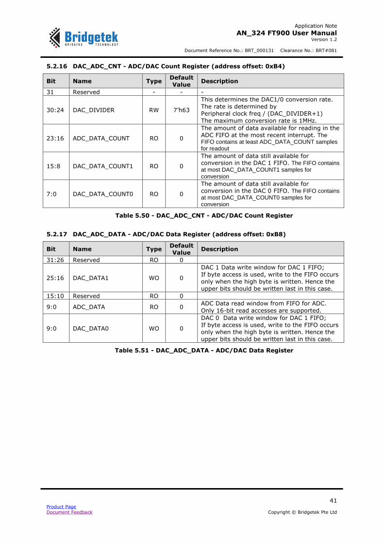
Application Note
AN_324 FT900 User Manual Version 1.2
Document Reference No.: BRT_000131 Clearance No.: BRT#081
41 Product Page Document Feedback Copyright © Bridgetek Pte Ltd
5.2.16 DAC_ADC_CNT - ADC/DAC Count Register (address offset: 0xB4)
Bit Name Type Default Value
Description
31 Reserved - - -
30:24 DAC_DIVIDER RW 7’h63
This determines the DAC1/0 conversion rate. The rate is determined by Peripheral clock freq / (DAC_DIVIDER+1) The maximum conversion rate is 1MHz.
23:16 ADC_DATA_COUNT RO 0
The amount of data available for reading in the ADC FIFO at the most recent interrupt. The FIFO contains at least ADC_DATA_COUNT samples for readout
15:8 DAC_DATA_COUNT1 RO 0
The amount of data still available for conversion in the DAC 1 FIFO. The FIFO contains at most DAC_DATA_COUNT1 samples for conversion
7:0 DAC_DATA_COUNT0 RO 0
The amount of data still available for conversion in the DAC 0 FIFO. The FIFO contains at most DAC_DATA_COUNT0 samples for conversion
Table 5.50 - DAC_ADC_CNT - ADC/DAC Count Register
5.2.17 DAC_ADC_DATA - ADC/DAC Data Register (address offset: 0xB8)
Bit Name Type Default Value
Description
31:26 Reserved RO 0
25:16 DAC_DATA1 WO 0
DAC 1 Data write window for DAC 1 FIFO; If byte access is used, write to the FIFO occurs
only when the high byte is written. Hence the upper bits should be written last in this case.
15:10 Reserved RO 0
9:0 ADC_DATA RO 0 ADC Data read window from FIFO for ADC.
Only 16-bit read accesses are supported.
9:0 DAC_DATA0 WO 0
DAC 0 Data write window for DAC 1 FIFO; If byte access is used, write to the FIFO occurs only when the high byte is written. Hence the upper bits should be written last in this case.
Table 5.51 - DAC_ADC_DATA - ADC/DAC Data Register

Application Note
AN_324 FT900 User Manual Version 1.2
Document Reference No.: BRT_000131 Clearance No.: BRT#081
42 Product Page Document Feedback Copyright © Bridgetek Pte Ltd
6 Interrupt Controller
The interrupt controller takes in 32 interrupts, and based on the interrupt priorities assigned generates the interrupt to the FT900 together with an ISR address. Nested interrupts are allowed if
enabled. By default it is disabled. Up to 16 levels of nesting is allowed which defaults to only 1 level if nesting is enabled.
When nesting is enabled, only interrupts with higher priorities can interrupt the current interrupt. Interrupts of same or lower priorities will be queued as long as the interrupt sources are not cleared.
The ISR vectors range from 0 to 31, corresponding to interrupts 0 to 31. The actual ISR address
corresponds to program memory addresses 2 to 33.
The highest priority interrupt by default is interrupt input 0, and the lowest interrupt input is 31. The priorities however can be rearranged by setting the appropriate registers. Each interrupt input is assigned an interrupt priority position that can be changed. Note it’s possible to assign multiple interrupts to the same priority. By default the interrupts 0 to 31 are assigned interrupt priorities 0
to 31 respectively, with lower number indicating higher priority.
A global interrupt mask bit is also available. Setting it to 1 will temporarily block all
interrupts except the interrupt assigned as interrupt 0 which is non-maskable by this global mask.
In the FT900, the interrupts connections from the peripherals are listed in the table below. Interrupts 23 to 31 are unused by default.
Peripheral Interrupt
Interrupt Controller
Interrupt Input
Number
Default Priority
Power Management 0 0 (Highest) – Non-maskable
USB Host 1 1
USB Peripheral 2 2
Ethernet 3 3
SD Host 4 4
CAN 0 5 5
CAN 1 6 6
Data Capture Interface 7 7
SPI Master 8 8
SPI Slave 0 9 9
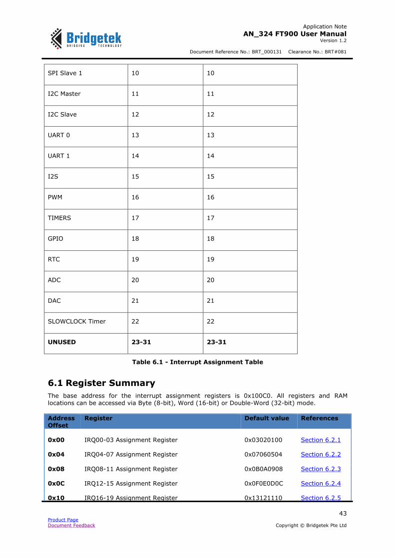
Application Note
AN_324 FT900 User Manual Version 1.2
Document Reference No.: BRT_000131 Clearance No.: BRT#081
43 Product Page Document Feedback Copyright © Bridgetek Pte Ltd
SPI Slave 1 10 10
I2C Master 11 11
I2C Slave 12 12
UART 0 13 13
UART 1 14 14
I2S 15 15
PWM 16 16
TIMERS 17 17
GPIO 18 18
RTC 19 19
ADC 20 20
DAC 21 21
SLOWCLOCK Timer 22 22
UNUSED 23-31 23-31
Table 6.1 - Interrupt Assignment Table
6.1 Register Summary
The base address for the interrupt assignment registers is 0x100C0. All registers and RAM locations can be accessed via Byte (8-bit), Word (16-bit) or Double-Word (32-bit) mode.
Address Offset
Register
Default value
References
0x00 IRQ00-03 Assignment Register 0x03020100 Section 6.2.1
0x04 IRQ04-07 Assignment Register 0x07060504 Section 6.2.2
0x08 IRQ08-11 Assignment Register 0x0B0A0908 Section 6.2.3
0x0C IRQ12-15 Assignment Register 0x0F0E0D0C Section 6.2.4
0x10 IRQ16-19 Assignment Register 0x13121110 Section 6.2.5
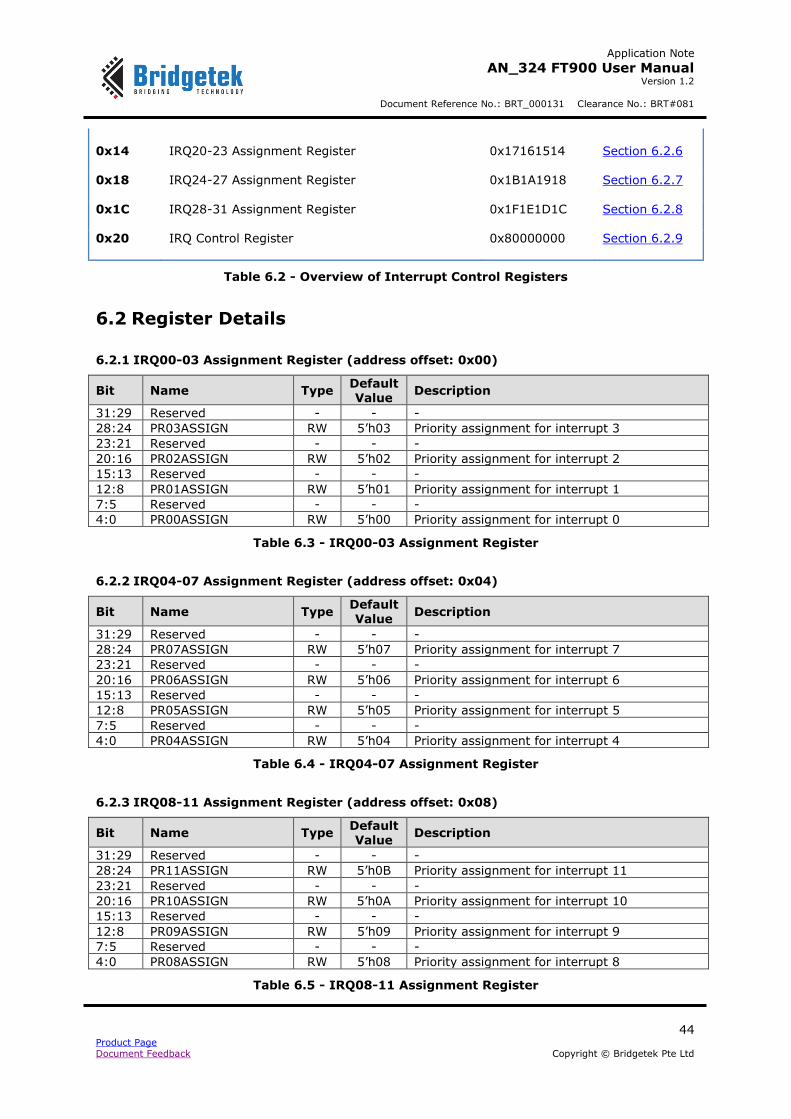
Application Note
AN_324 FT900 User Manual Version 1.2
Document Reference No.: BRT_000131 Clearance No.: BRT#081
44 Product Page Document Feedback Copyright © Bridgetek Pte Ltd
0x14 IRQ20-23 Assignment Register 0x17161514 Section 6.2.6
0x18 IRQ24-27 Assignment Register 0x1B1A1918 Section 6.2.7
0x1C IRQ28-31 Assignment Register 0x1F1E1D1C Section 6.2.8
0x20 IRQ Control Register 0x80000000 Section 6.2.9
Table 6.2 - Overview of Interrupt Control Registers
6.2 Register Details
6.2.1 IRQ00-03 Assignment Register (address offset: 0x00)
Bit Name Type Default Value
Description
31:29 Reserved - - -
28:24 PR03ASSIGN RW 5’h03 Priority assignment for interrupt 3
23:21 Reserved - - -
20:16 PR02ASSIGN RW 5’h02 Priority assignment for interrupt 2
15:13 Reserved - - -
12:8 PR01ASSIGN RW 5’h01 Priority assignment for interrupt 1
7:5 Reserved - - -
4:0 PR00ASSIGN RW 5’h00 Priority assignment for interrupt 0
Table 6.3 - IRQ00-03 Assignment Register
6.2.2 IRQ04-07 Assignment Register (address offset: 0x04)
Bit Name Type Default Value
Description
31:29 Reserved - - -
28:24 PR07ASSIGN RW 5’h07 Priority assignment for interrupt 7
23:21 Reserved - - -
20:16 PR06ASSIGN RW 5’h06 Priority assignment for interrupt 6
15:13 Reserved - - -
12:8 PR05ASSIGN RW 5’h05 Priority assignment for interrupt 5
7:5 Reserved - - -
4:0 PR04ASSIGN RW 5’h04 Priority assignment for interrupt 4
Table 6.4 - IRQ04-07 Assignment Register
6.2.3 IRQ08-11 Assignment Register (address offset: 0x08)
Bit Name Type Default Value
Description
31:29 Reserved - - -
28:24 PR11ASSIGN RW 5’h0B Priority assignment for interrupt 11
23:21 Reserved - - -
20:16 PR10ASSIGN RW 5’h0A Priority assignment for interrupt 10
15:13 Reserved - - -
12:8 PR09ASSIGN RW 5’h09 Priority assignment for interrupt 9
7:5 Reserved - - -
4:0 PR08ASSIGN RW 5’h08 Priority assignment for interrupt 8
Table 6.5 - IRQ08-11 Assignment Register
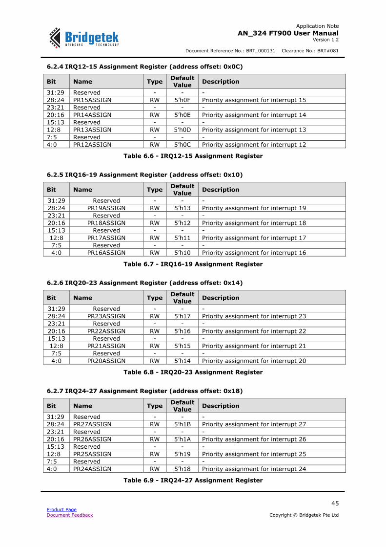
Application Note
AN_324 FT900 User Manual Version 1.2
Document Reference No.: BRT_000131 Clearance No.: BRT#081
45 Product Page Document Feedback Copyright © Bridgetek Pte Ltd
6.2.4 IRQ12-15 Assignment Register (address offset: 0x0C)
Bit Name Type Default Value
Description
31:29 Reserved - - -
28:24 PR15ASSIGN RW 5’h0F Priority assignment for interrupt 15
23:21 Reserved - - -
20:16 PR14ASSIGN RW 5’h0E Priority assignment for interrupt 14
15:13 Reserved - - -
12:8 PR13ASSIGN RW 5’h0D Priority assignment for interrupt 13
7:5 Reserved - - -
4:0 PR12ASSIGN RW 5’h0C Priority assignment for interrupt 12
Table 6.6 - IRQ12-15 Assignment Register
6.2.5 IRQ16-19 Assignment Register (address offset: 0x10)
Bit Name Type Default Value
Description
31:29 Reserved - - -
28:24 PR19ASSIGN RW 5’h13 Priority assignment for interrupt 19
23:21 Reserved - - -
20:16 PR18ASSIGN RW 5’h12 Priority assignment for interrupt 18
15:13 Reserved - - -
12:8 PR17ASSIGN RW 5’h11 Priority assignment for interrupt 17
7:5 Reserved - - -
4:0 PR16ASSIGN RW 5’h10 Priority assignment for interrupt 16
Table 6.7 - IRQ16-19 Assignment Register
6.2.6 IRQ20-23 Assignment Register (address offset: 0x14)
Bit Name Type Default Value
Description
31:29 Reserved - - -
28:24 PR23ASSIGN RW 5’h17 Priority assignment for interrupt 23
23:21 Reserved - - -
20:16 PR22ASSIGN RW 5’h16 Priority assignment for interrupt 22
15:13 Reserved - - -
12:8 PR21ASSIGN RW 5’h15 Priority assignment for interrupt 21
7:5 Reserved - - -
4:0 PR20ASSIGN RW 5’h14 Priority assignment for interrupt 20
Table 6.8 - IRQ20-23 Assignment Register
6.2.7 IRQ24-27 Assignment Register (address offset: 0x18)
Bit Name Type Default Value
Description
31:29 Reserved - - -
28:24 PR27ASSIGN RW 5’h1B Priority assignment for interrupt 27
23:21 Reserved - - -
20:16 PR26ASSIGN RW 5’h1A Priority assignment for interrupt 26
15:13 Reserved - - -
12:8 PR25ASSIGN RW 5’h19 Priority assignment for interrupt 25
7:5 Reserved - - -
4:0 PR24ASSIGN RW 5’h18 Priority assignment for interrupt 24
Table 6.9 - IRQ24-27 Assignment Register

Application Note
AN_324 FT900 User Manual Version 1.2
Document Reference No.: BRT_000131 Clearance No.: BRT#081
46 Product Page Document Feedback Copyright © Bridgetek Pte Ltd
6.2.8 IRQ28-31 Assignment Register (address offset: 0x1C)
Bit Name Type Default Value
Description
31:29 Reserved - - -
28:24 PR31ASSIGN RW 5’h1F Priority assignment for interrupt 31
23:21 Reserved - - -
20:16 PR30ASSIGN RW 5’h1E Priority assignment for interrupt 30
15:13 Reserved - - -
12:8 PR29ASSIGN RW 5’h1D Priority assignment for interrupt 29
7:5 Reserved - - -
4:0 PR28ASSIGN RW 5’h1C Priority assignment for interrupt 28
Table 6.10 - IRQ28-31 Assignment Register
6.2.9 IRQ Control Register (address offset: 0x20)
Bit Name Type Default Value
Description
31 Global Interrupt Mask RW 1 Set to 1 to mask all interrupts.
30:8 Reserved - - -
7 Nested Interrupt RW 0 Set to 1 to enable nested interrupts. This bit shall be set or cleared while the Global Interrupt Mask is enabled.
6:4 Reserved - - -
3:0 Nested Depth RW 4’h00 Maximum number of nested interrupts permitted (Nested Depth + 1); minimum 1 level, and maximum 16 levels.
Table 6.11 - IRQ Control Register

Application Note
AN_324 FT900 User Manual Version 1.2
Document Reference No.: BRT_000131 Clearance No.: BRT#081
47 Product Page Document Feedback Copyright © Bridgetek Pte Ltd
7 EFUSE
7.1 Introduction
The EFUSE is the only way to modify the content of the Chip Configuration Register.
There are 64 bits in the EFUSE, in which the lower 32 bits correspond to the 32 bits in the register.
Please note that only bits 27..0 should be modified by the EFUSE operation described below.
The EFUSE can be accessed externally via the first SPI slave interface (SPI Slave 1) while RESET is active. The supported mode is CPOL = 0 and CPHA = 0.
For the data transfer, a read operation reads all EFUSE bits at a time while a write operation writes each individual EFUSE bit separately.
Warning: Each EFUSE bit can only be written (or blown) once. After the bit has been blown, there
is no way to revert it.
7.2 EFUSE Operation
To use the interface to access the EFUSE, send in “EFU” as the first 3 bytes.
To read from the EFUSE, send in the command 0x80. 8 dummy clocks are needed to perform the
EFUSE read; another 64 dummy clocks must be provided to shift out the 64-bit EFUSE contents, with the MSB first.
To write to the EFUSE, send in the command 0x08, followed by 8-bit address (only the lower 6 bits are effective). A dummy byte should follow that.
After the required programming period (~500us) has elapsed, a non-zero byte should be sent in to terminate the programming cycle. The programming will not terminate automatically. CS signal
shall remain asserted throughout until the last termination byte is transmitted.
7.3 EFUSE bits
The table below shows the 64 bits. The bit number acts as the bit address for the write operation.
Bit Name Description
27 1-Wire_ACTIVE If set, FTDI 1-wire debug interface is available; otherwise it’s permanently disabled.
26 EXT_SPI_ACTIVE If set, internal FLASH/EFUSE can be accessed via SPI Slave 1 interface during reset; otherwise this interface is permanently disabled.
25:21 Reserved -
20 FLASH_RD_ENA If set, FLASH read via the external SPI interface is allowed; otherwise this feature is permanently disabled. Write will still be available; but see bits 19-16
19 FLASH_WR_B3_ENA If set, FLASH write/erase to bytes 196608 – 262143 is allowed; otherwise it is permanently non-writable/non-erasable.
18 FLASH_WR_B2_ENA
If set, FLASH write/erase to bytes 131072 – 196607 is
allowed; otherwise it is permanently non-writable/non-erasable.
17 FLASH_WR_B1_ENA If set, FLASH write/erase to bytes 65536 – 131071 is allowed; otherwise it is permanently non-writable/non-erasable.
16 FLASH_WR_B0_ENA If set, FLASH write/erase to bytes 0 – 65535 is allowed; otherwise it is permanently non-writable/non-erasable.
15:0 FLASH_CODE_RD Each bit corresponds 16kB of FLASH location, with bit 0
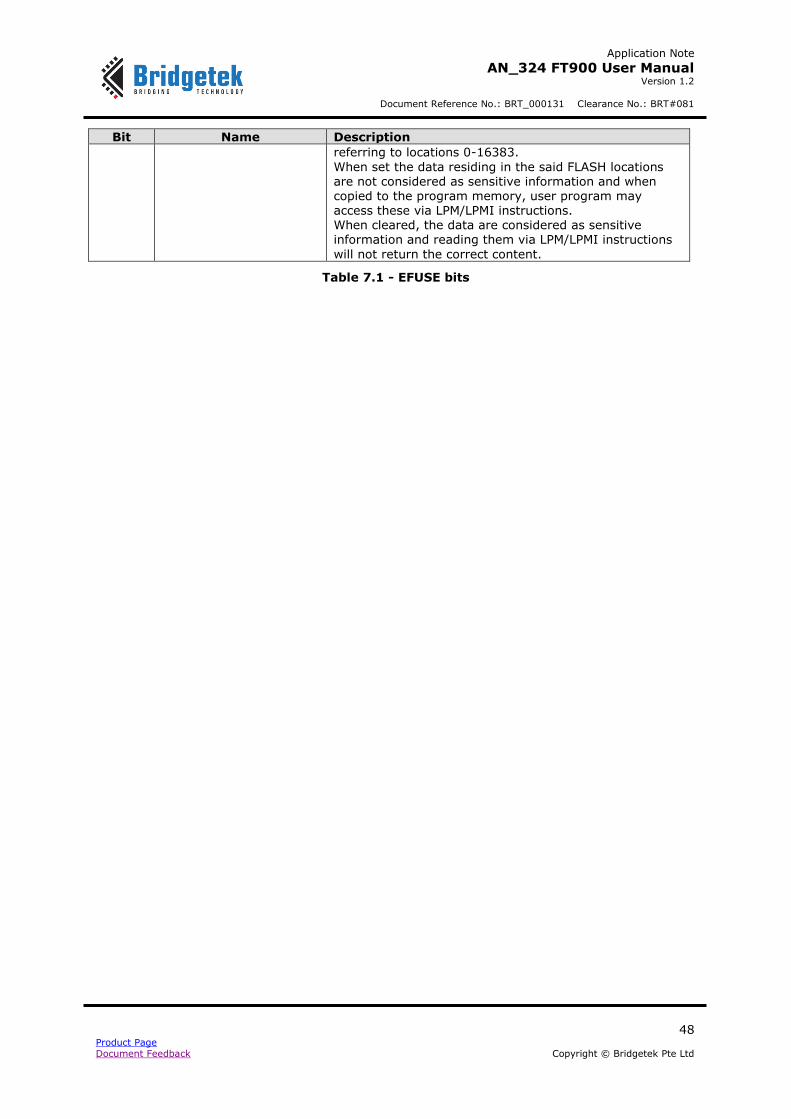
Application Note
AN_324 FT900 User Manual Version 1.2
Document Reference No.: BRT_000131 Clearance No.: BRT#081
48 Product Page Document Feedback Copyright © Bridgetek Pte Ltd
Bit Name Description
referring to locations 0-16383.
When set the data residing in the said FLASH locations are not considered as sensitive information and when copied to the program memory, user program may access these via LPM/LPMI instructions. When cleared, the data are considered as sensitive information and reading them via LPM/LPMI instructions
will not return the correct content.
Table 7.1 - EFUSE bits

Application Note
AN_324 FT900 User Manual Version 1.2
Document Reference No.: BRT_000131 Clearance No.: BRT#081
49 Product Page Document Feedback Copyright © Bridgetek Pte Ltd
8 USB Host
This is a single -port USB host controller which is compliant with the USB 2.0 specification and compatible with the Enhanced Host Controller Interface (EHCI) specification. It supports HS/FS/LS transactions, control/bulk/interrupt/isochronous transfers and split-transaction of the hub. An 8 kB RAM arranged as (2 kB x 32) is attached to the host as buffers.
8.1 Register Summary
Listed below are the registers with their offset from the base address (0x10100). All registers and RAM locations can be accessed via Byte (8-bit), Word (16-bit) or Double-Word (32-bit) mode.
Address Offset
Register Default value References
EHCI Operational Registers
0x00 HC Capability Register 0x01000010 Section 8.2.1
0x04 HCSPARAMS – HC Structural Parameters 0x00000001 Section 8.2.2
0x08 HCCPARAMS – HC Capability Parameters 0x00000006 Section 8.2.3
0x10 USBCMD – HC USB Command Register 0x00080B00 Section 8.2.4
0x14 USBSTS – HC USB Status Register 0x00001000 Section 8.2.5
0x18 USBINTR – HC USB Interrupt Enable Register 0x00000000 Section 8.2.6
0x1C FRINDEX – HC Frame Index Register 0x00000000 Section 8.2.7
0x24 PERIODICLISTBASE – HC Periodic Frame List Base
Address Register
0x00000000 Section 8.2.8
0x28 ASYNCLISTADDR – HC Current Asynchronous List Address Register
0x00000000 Section 8.2.9
0x30 PORTSC – HC Port Status and Control Register 0x00000000 Section 8.2.10
Configuration Registers
0x34 EOF Time & Asynchronous Schedule Sleep Timer
Register
0x00000041 Section 8.3.1
0x40 Bus Monitor Control / Status Register 0x00000000 Section 8.3.2
0x78 HPROT – Master Protection Information Setting Register
0x00000003 Section 8.3.3
USB Testing Registers
0x54 Vendor Specific IO Control Register 0x00000020 Section 8.4.1
0x58 Vendor Specific Status Register 0xXXXXXXXX Section 8.4.2
0x50 Test Register 0x00000000 Section 8.4.3
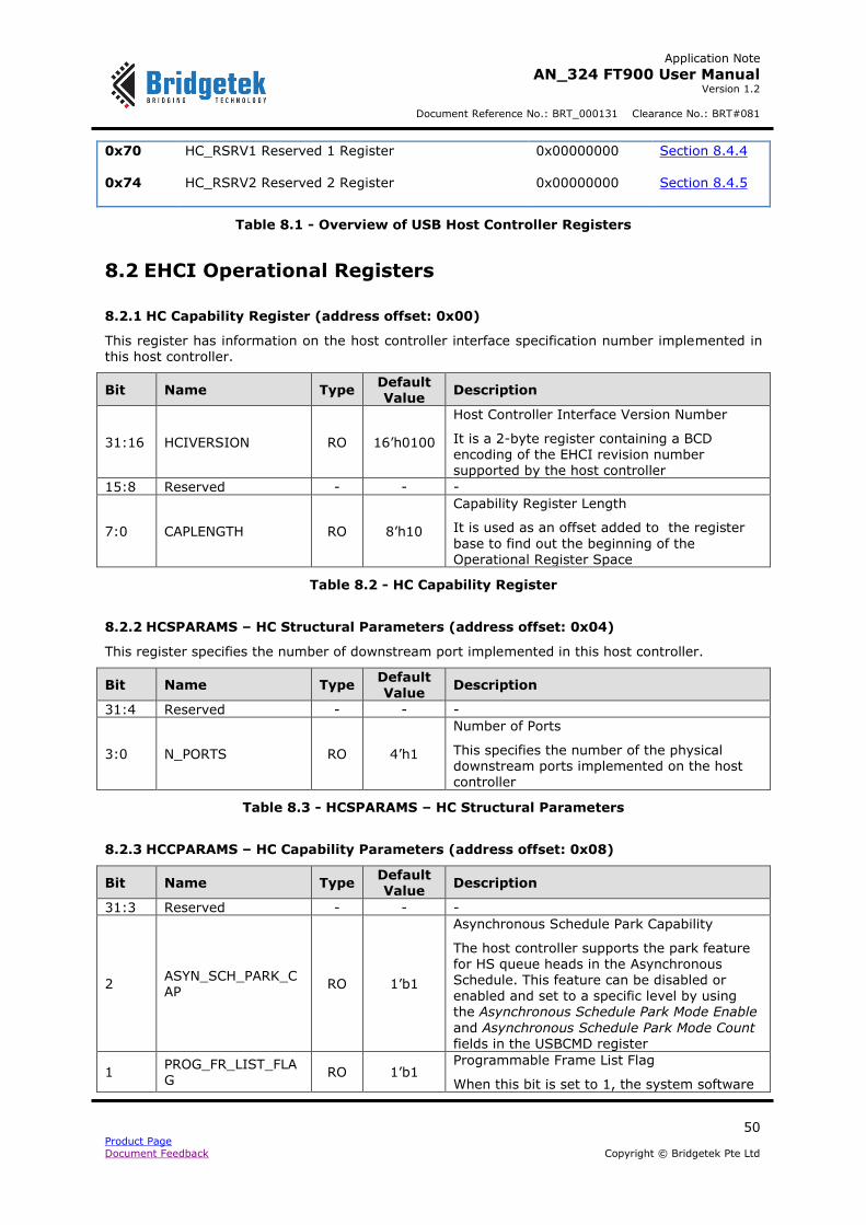
Application Note
AN_324 FT900 User Manual Version 1.2
Document Reference No.: BRT_000131 Clearance No.: BRT#081
50 Product Page Document Feedback Copyright © Bridgetek Pte Ltd
0x70 HC_RSRV1 Reserved 1 Register 0x00000000 Section 8.4.4
0x74 HC_RSRV2 Reserved 2 Register 0x00000000 Section 8.4.5
Table 8.1 - Overview of USB Host Controller Registers
8.2 EHCI Operational Registers
8.2.1 HC Capability Register (address offset: 0x00)
This register has information on the host controller interface specification number implemented in this host controller.
Bit Name Type Default Value
Description
31:16 HCIVERSION RO 16’h0100
Host Controller Interface Version Number
It is a 2-byte register containing a BCD encoding of the EHCI revision number supported by the host controller
15:8 Reserved - - -
7:0 CAPLENGTH RO 8’h10
Capability Register Length
It is used as an offset added to the register
base to find out the beginning of the Operational Register Space
Table 8.2 - HC Capability Register
8.2.2 HCSPARAMS – HC Structural Parameters (address offset: 0x04)
This register specifies the number of downstream port implemented in this host controller.
Bit Name Type Default
Value Description
31:4 Reserved - - -
3:0 N_PORTS RO 4’h1
Number of Ports
This specifies the number of the physical downstream ports implemented on the host controller
Table 8.3 - HCSPARAMS – HC Structural Parameters
8.2.3 HCCPARAMS – HC Capability Parameters (address offset: 0x08)
Bit Name Type Default Value
Description
31:3 Reserved - - -
2 ASYN_SCH_PARK_CAP
RO 1’b1
Asynchronous Schedule Park Capability
The host controller supports the park feature
for HS queue heads in the Asynchronous Schedule. This feature can be disabled or enabled and set to a specific level by using the Asynchronous Schedule Park Mode Enable
and Asynchronous Schedule Park Mode Count fields in the USBCMD register
1 PROG_FR_LIST_FLAG
RO 1’b1 Programmable Frame List Flag
When this bit is set to 1, the system software

Application Note
AN_324 FT900 User Manual Version 1.2
Document Reference No.: BRT_000131 Clearance No.: BRT#081
51 Product Page Document Feedback Copyright © Bridgetek Pte Ltd
Bit Name Type Default Value
Description
can specify and use a smaller frame list and configure the host controller via Frame List Size field of the USBCMD register. This requirement ensures that the frame list is always physically contiguous.
0 Reserved - - -
Table 8.4 - HCCPARAMS – HC Capability Parameters
8.2.4 USBCMD – HC USB Command Register (address offset: 0x10)
The command register is used by the software to schedule the command to be executed by the USB host controller hardware.
Bit Name Type Default
Value Description
31:24 Reserved - - -
23:16 INT_THRC RW 8’h08
Interrupt Threshold Control
This is used by the system software to select the maximum rate at which the host controller will issue the interrupts. The only valid values are as below:
0x00: Reserved 0x01: 1 micro-frame (125us) 0x02: 2 micro-frames (250us) 0x04: 4 micro-frames (500us) 0x08: 8 micro-frames (default: 1ms) 0x10: 16 micro-frames (2ms)
0x20: 32 micro-frames (4ms) 0x40: 64 micro-frames (8ms)
Note: In the FS mode, these bits are
reserved. 15:12 Reserved - - -
11 ASYN_PK_EN RW 1’b1
Asynchronous Schedule Park Mode Enable
Software uses this to enable or disable the Park mode. When this is set to 1, the Park mode is enabled
10 Reserved - - -
9:8 ASYN_PK_CNT RW 2’h3
Asynchronous Schedule Park Mode Count
This contains a count for the number of successive transactions that the host controller is allowed to execute from a high speed queue head on the asynchronous schedule.
7 Reserved - - -
6 INT_OAAD RW 1’b0
Interrupt on Asynchronous Advance Doorbell
This is used as a doorbell by software to ring
the host controller to issue and interrupt at the next advance of the synchronous schedule.
5 ASCH_EN RW 1’b0
Asynchronous Schedule Enable
This controls whether the host controller skips the processing of asynchronous schedule.
0: Do not process the asynchronous schedule
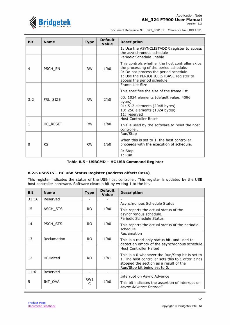
Application Note
AN_324 FT900 User Manual Version 1.2
Document Reference No.: BRT_000131 Clearance No.: BRT#081
52 Product Page Document Feedback Copyright © Bridgetek Pte Ltd
Bit Name Type Default Value
Description
1: Use the ASYNCLISTADDR register to access the asynchronous schedule
4 PSCH_EN RW 1’b0
Periodic Schedule Enable
This controls whether the host controller skips the processing of the period schedule. 0: Do not process the period schedule 1: Use the PERIODICLISTBASE register to access the period schedule
3:2 FRL_SIZE RW 2’h0
Frame List Size
This specifies the size of the frame list.
00: 1024 elements (default value, 4096 bytes) 01: 512 elements (2048 bytes)
10: 256 elements (1024 bytes) 11: reserved
1 HC_RESET RW 1’b0
Host Controller Reset
This is used by the software to reset the host controller.
0 RS RW 1’b0
Run/Stop
When this is set to 1, the host controller proceeds with the execution of schedule.
0: Stop 1: Run
Table 8.5 - USBCMD – HC USB Command Register
8.2.5 USBSTS – HC USB Status Register (address offset: 0x14)
This register indicates the status of the USB host controller. This register is updated by the USB
host controller hardware. Software clears a bit by writing 1 to the bit.
Bit Name Type Default
Value Description
31:16 Reserved - - -
15 ASCH_STS RO 1’b0
Asynchronous Schedule Status
This reports the actual status of the asynchronous schedule.
14 PSCH_STS RO 1’b0
Periodic Schedule Status
This reports the actual status of the periodic schedule.
13 Reclamation RO 1’b0
Reclamation
This is a read-only status bit, and used to detect an empty of the asynchronous schedule
12 HCHalted RO 1’b1
Host Controller Halted
This is a 0 whenever the Run/Stop bit is set to 1. The host controller sets this to 1 after it has stopped the section as a result of the Run/Stop bit being set to 0.
11:6 Reserved - - -
5 INT_OAA RW1
C 1’b0
Interrupt on Async Advance
This bit indicates the assertion of interrupt on Async Advance Doorbell

Application Note
AN_324 FT900 User Manual Version 1.2
Document Reference No.: BRT_000131 Clearance No.: BRT#081
53 Product Page Document Feedback Copyright © Bridgetek Pte Ltd
Bit Name Type Default Value
Description
4 H_SYSERR RW1
C 1’b0
Host System Error
The host controller sets this to 1 when a serious error occurs during a host system
access involving the host controller module.
3 FRL_ROL RW1
C 1’b0
Frame List Rollover
The host controller sets this to 1 when the Frame List Index rolls over from its maximum value to zero.
2 PO_CHG_DET RW1
C 1’b0
Port Change Detect
The host controller sets this to 1 when any port has a change bit transition from 0 to 1. In addition, this bit is loaded with the OR of all of the PORTSC change bits.
1 USBERR_INT RW1
C 1’b0
USB Error Interrupt
The host controller sets this to 1 when the
completion of a USB transaction results in an error condition
0 USB_INT RW1
C 1’b0
USB Interrupt
The host controller sets this to 1 upon completion of a USB transaction
Table 8.6 - USBSTS – HC USB Status Register
8.2.6 USBINTR – HC USB Interrupt Enable Register (address offset: 0x18)
This register enables the required host controller interrupts. The interrupts enabled by this register toggle the interrupt pin when the interrupt condition occurs. Interrupts not enabled in this register do not toggle the interrupt pin but the status can be read by polling the interrupt status register.
Bit Name Type Default
Value Description
31:6 Reserved - - -
5 INT_OAA_EN RW 1’b0
Interrupt on Async Advance Enable
When this is 1 and the Interrupt on Async Advance bit in the USBSTS register is 1, the host controller will issue an interrupt at the next interrupt threshold.
4 H_SYSERR_EN RW 1’b0
Host System Error Enable
When this is 1 and the Host System Error Status bit in the USBSTS register is 1, the host controller will issue an interrupt at the
next interrupt threshold.
3 FRL_ROL_EN RW 1’b0
Frame List Rollover Enable
When this is 1 and the Frame List Rollover bit in the USBSTS register is 1, the host
controller will issue an interrupt at the next interrupt threshold.
2 PO_CHG_INT_EN RW 1’b0
Port Change Interrupt Enable
When this is 1 and the Port Change Detect bit in the USBSTS register is 1, the host controller will issue an interrupt at the next
interrupt threshold.
1 USBERR_INT_EN RW 1’b0 USB Error Interrupt Enable
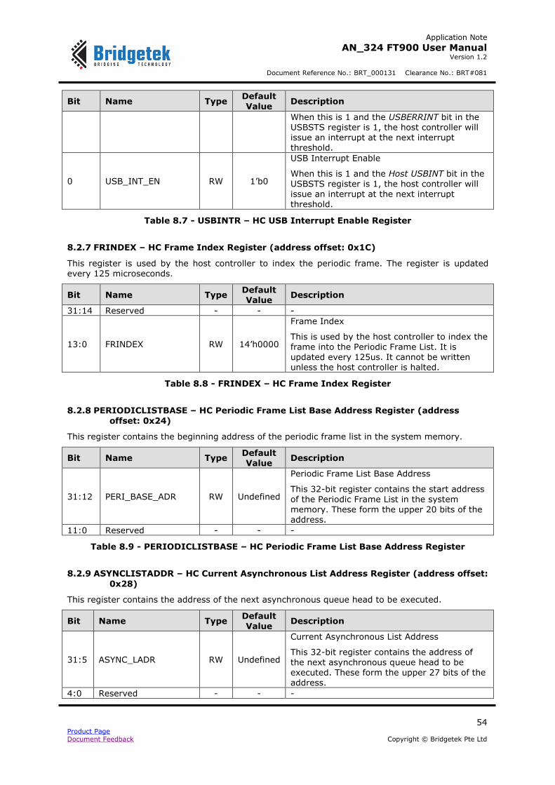
Application Note
AN_324 FT900 User Manual Version 1.2
Document Reference No.: BRT_000131 Clearance No.: BRT#081
54 Product Page Document Feedback Copyright © Bridgetek Pte Ltd
Bit Name Type Default Value
Description
When this is 1 and the USBERRINT bit in the USBSTS register is 1, the host controller will issue an interrupt at the next interrupt threshold.
0 USB_INT_EN RW 1’b0
USB Interrupt Enable
When this is 1 and the Host USBINT bit in the USBSTS register is 1, the host controller will issue an interrupt at the next interrupt threshold.
Table 8.7 - USBINTR – HC USB Interrupt Enable Register
8.2.7 FRINDEX – HC Frame Index Register (address offset: 0x1C)
This register is used by the host controller to index the periodic frame. The register is updated every 125 microseconds.
Bit Name Type Default Value
Description
31:14 Reserved - - -
13:0 FRINDEX RW 14’h0000
Frame Index
This is used by the host controller to index the frame into the Periodic Frame List. It is updated every 125us. It cannot be written unless the host controller is halted.
Table 8.8 - FRINDEX – HC Frame Index Register
8.2.8 PERIODICLISTBASE – HC Periodic Frame List Base Address Register (address
offset: 0x24)
This register contains the beginning address of the periodic frame list in the system memory.
Bit Name Type Default Value
Description
31:12 PERI_BASE_ADR RW Undefined
Periodic Frame List Base Address
This 32-bit register contains the start address of the Periodic Frame List in the system memory. These form the upper 20 bits of the address.
11:0 Reserved - - -
Table 8.9 - PERIODICLISTBASE – HC Periodic Frame List Base Address Register
8.2.9 ASYNCLISTADDR – HC Current Asynchronous List Address Register (address offset:
0x28)
This register contains the address of the next asynchronous queue head to be executed.
Bit Name Type Default Value
Description
31:5 ASYNC_LADR RW Undefined
Current Asynchronous List Address
This 32-bit register contains the address of the next asynchronous queue head to be executed. These form the upper 27 bits of the address.
4:0 Reserved - - -
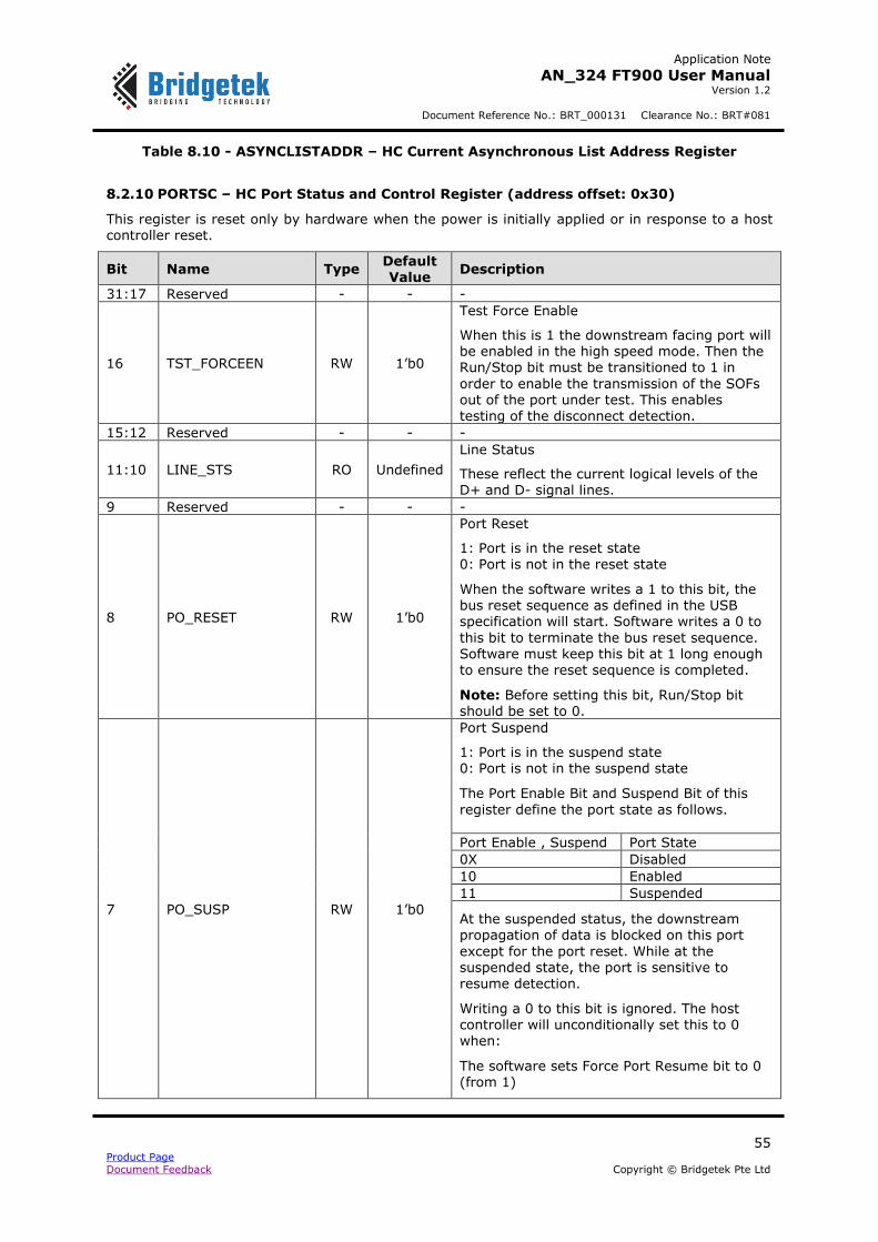
Application Note
AN_324 FT900 User Manual Version 1.2
Document Reference No.: BRT_000131 Clearance No.: BRT#081
55 Product Page Document Feedback Copyright © Bridgetek Pte Ltd
Table 8.10 - ASYNCLISTADDR – HC Current Asynchronous List Address Register
8.2.10 PORTSC – HC Port Status and Control Register (address offset: 0x30)
This register is reset only by hardware when the power is initially applied or in response to a host controller reset.
Bit Name Type Default Value
Description
31:17 Reserved - - -
16 TST_FORCEEN RW 1’b0
Test Force Enable
When this is 1 the downstream facing port will be enabled in the high speed mode. Then the Run/Stop bit must be transitioned to 1 in
order to enable the transmission of the SOFs out of the port under test. This enables
testing of the disconnect detection.
15:12 Reserved - - -
11:10 LINE_STS RO Undefined
Line Status
These reflect the current logical levels of the D+ and D- signal lines.
9 Reserved - - -
8 PO_RESET RW 1’b0
Port Reset
1: Port is in the reset state 0: Port is not in the reset state
When the software writes a 1 to this bit, the bus reset sequence as defined in the USB specification will start. Software writes a 0 to
this bit to terminate the bus reset sequence. Software must keep this bit at 1 long enough to ensure the reset sequence is completed.
Note: Before setting this bit, Run/Stop bit should be set to 0.
7 PO_SUSP RW 1’b0
Port Suspend
1: Port is in the suspend state 0: Port is not in the suspend state
The Port Enable Bit and Suspend Bit of this
register define the port state as follows.
Port Enable , Suspend Port State
0X Disabled
10 Enabled
11 Suspended
At the suspended status, the downstream propagation of data is blocked on this port
except for the port reset. While at the suspended state, the port is sensitive to
resume detection.
Writing a 0 to this bit is ignored. The host controller will unconditionally set this to 0 when:
The software sets Force Port Resume bit to 0 (from 1)
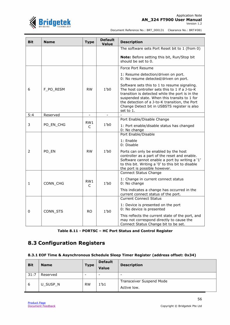
Application Note
AN_324 FT900 User Manual Version 1.2
Document Reference No.: BRT_000131 Clearance No.: BRT#081
56 Product Page Document Feedback Copyright © Bridgetek Pte Ltd
Bit Name Type Default Value
Description
The software sets Port Reset bit to 1 (from 0)
Note: Before setting this bit, Run/Stop bit should be set to 0.
6 F_PO_RESM RW 1’b0
Force Port Resume
1: Resume detection/driven on port.
0: No resume detected/driven on port.
Software sets this to 1 to resume signaling. The host controller sets this to 1 if a J-to-K transition is detected while the port is in the suspended state. When this transits to 1 for the detection of a J-to-K transition, the Port Change Detect bit in USBSTS register is also
set to 1.
5:4 Reserved - - -
3 PO_EN_CHG RW1
C 1’b0
Port Enable/Disable Change
1: Port enable/disable status has changed 0: No change
2 PO_EN RW 1’b0
Port Enable/Disable
1: Enable 0: Disable
Ports can only be enabled by the host
controller as a part of the reset and enable. Software cannot enable a port by writing a ‘1’ to this bit. Writing a ‘0’ to this bit to disable the port is possible however.
1 CONN_CHG RW1
C 1’b0
Connect Status Change
1: Change in current connect status
0: No change
This indicates a change has occurred in the
current connect status of the port.
0 CONN_STS RO 1’b0
Current Connect Status
1: Device is presented on the port 0: No device is presented
This reflects the current state of the port, and may not correspond directly to cause the Connect Status Change bit to be set.
Table 8.11 - PORTSC – HC Port Status and Control Register
8.3 Configuration Registers
8.3.1 EOF Time & Asynchronous Schedule Sleep Timer Register (address offset: 0x34)
Bit Name Type Default
Value Description
31:7 Reserved - - -
6 U_SUSP_N RW 1’b1 Transceiver Suspend Mode
Active low.
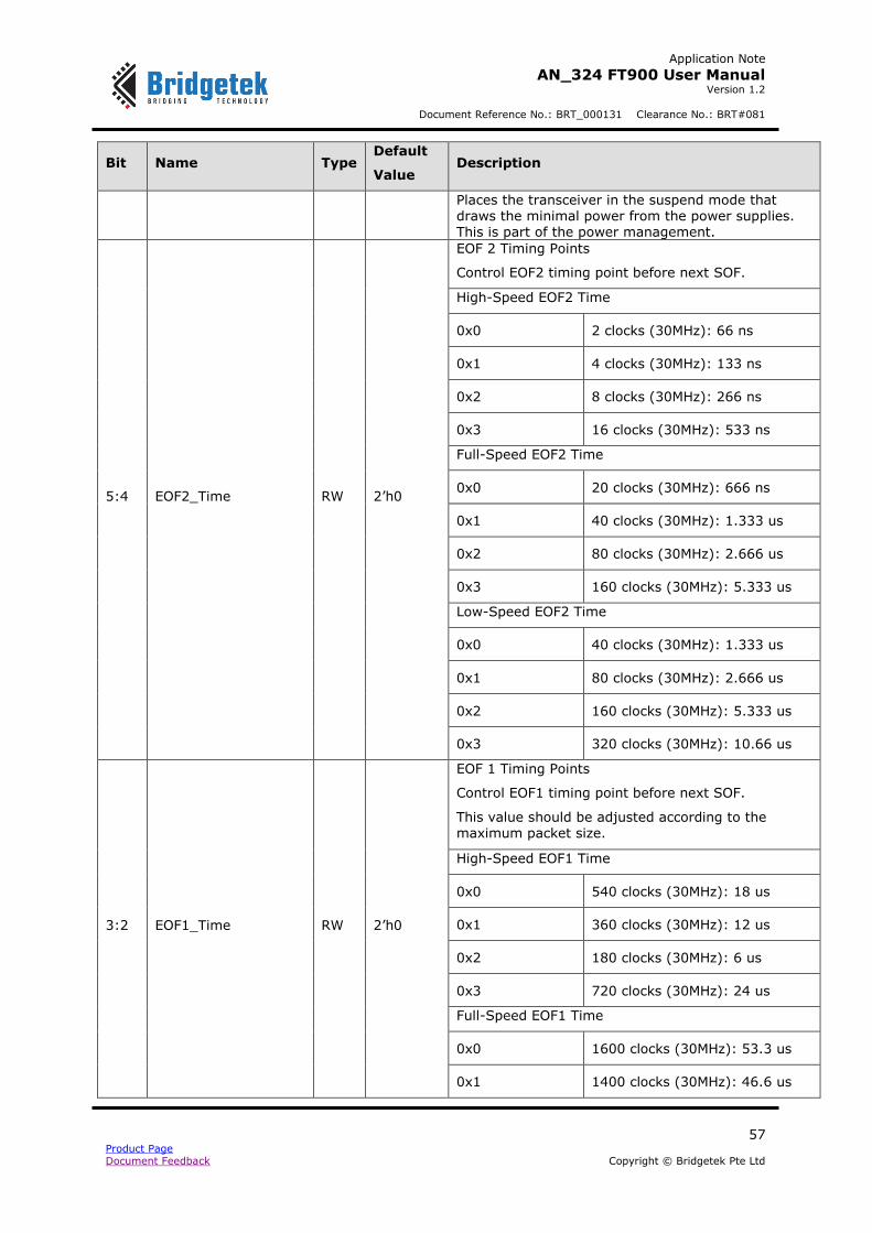
Application Note
AN_324 FT900 User Manual Version 1.2
Document Reference No.: BRT_000131 Clearance No.: BRT#081
57 Product Page Document Feedback Copyright © Bridgetek Pte Ltd
Bit Name Type Default
Value Description
Places the transceiver in the suspend mode that draws the minimal power from the power supplies. This is part of the power management.
5:4 EOF2_Time RW 2’h0
EOF 2 Timing Points
Control EOF2 timing point before next SOF.
High-Speed EOF2 Time
0x0 2 clocks (30MHz): 66 ns
0x1 4 clocks (30MHz): 133 ns
0x2 8 clocks (30MHz): 266 ns
0x3 16 clocks (30MHz): 533 ns
Full-Speed EOF2 Time
0x0 20 clocks (30MHz): 666 ns
0x1 40 clocks (30MHz): 1.333 us
0x2 80 clocks (30MHz): 2.666 us
0x3 160 clocks (30MHz): 5.333 us
Low-Speed EOF2 Time
0x0 40 clocks (30MHz): 1.333 us
0x1 80 clocks (30MHz): 2.666 us
0x2 160 clocks (30MHz): 5.333 us
0x3 320 clocks (30MHz): 10.66 us
3:2 EOF1_Time RW 2’h0
EOF 1 Timing Points
Control EOF1 timing point before next SOF.
This value should be adjusted according to the maximum packet size.
High-Speed EOF1 Time
0x0 540 clocks (30MHz): 18 us
0x1 360 clocks (30MHz): 12 us
0x2 180 clocks (30MHz): 6 us
0x3 720 clocks (30MHz): 24 us
Full-Speed EOF1 Time
0x0 1600 clocks (30MHz): 53.3 us
0x1 1400 clocks (30MHz): 46.6 us

Application Note
AN_324 FT900 User Manual Version 1.2
Document Reference No.: BRT_000131 Clearance No.: BRT#081
58 Product Page Document Feedback Copyright © Bridgetek Pte Ltd
Bit Name Type Default
Value Description
0x2 1200 clocks (30MHz): 40 us
0x3 21000 clocks (30MHz): 700 us
Low-Speed EOF1 Time
0x0 3750 clocks (30MHz): 125 us
0x1 3500 clocks (30MHz): 116 us
0x2 3250 clocks (30MHz): 108 us
0x3 4000 clocks (30MHz): 133 us
1:0 ASYN_SCH_SLPT RW 2’h1
Asynchronous Schedule Sleep Timer
Controls the Asynchronous Schedule sleep timer.
0x0 5 us
0x1 10 us
0x2 15 us
0x3 20 us
Table 8.12 - EOF Time & Asynchronous Schedule Sleep Timer Register
8.3.2 Bus Monitor Control / Status Register (address offset: 0x40)
Bit Name Type Default Value
Description
31:11 Reserved - - -
10:9 HOST_SPD_TYP RO 2’h0
Host Speed Type
0x2: HS 0x0: FS 0x1: LS 0x3: Reserved
8 VBUS_VLD RO 1’b0
VBUS Valid
When the voltage on the VBUS is above the valid VBUS threshold, this signal is valid.
7:5 - - - Reserved for testing only. They should remain as 0.
4 VBUS_OFF RW 1’b0
VBUS OFF
This controls the voltage on the VBUS_ON/OFF.
0: VBUS on 1: VBUS off
3:2 Reserved - - These bits should remain as 0.
1 HDISCON_FLT_SEL RW 1’b0
Select a timer to filter out noise on HDISCON from the UTMI+
0: Approximately 135 us 1: Approximately 270 us
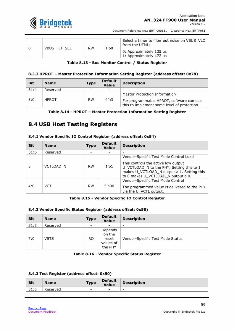
Application Note
AN_324 FT900 User Manual Version 1.2
Document Reference No.: BRT_000131 Clearance No.: BRT#081
59 Product Page Document Feedback Copyright © Bridgetek Pte Ltd
0 VBUS_FLT_SEL RW 1’b0
Select a timer to filter out noise on VBUS_VLD from the UTMI+
0: Approximately 135 us 1: Approximately 472 us
Table 8.13 - Bus Monitor Control / Status Register
8.3.3 HPROT – Master Protection Information Setting Register (address offset: 0x78)
Bit Name Type Default Value
Description
31:4 Reserved - - -
3:0 HPROT RW 4’h3
Master Protection Information
For programmable HPROT, software can use this to implement some level of protection.
Table 8.14 - HPROT – Master Protection Information Setting Register
8.4 USB Host Testing Registers
8.4.1 Vendor Specific IO Control Register (address offset: 0x54)
Bit Name Type Default
Value Description
31:6 Reserved - - -
5 VCTLOAD_N RW 1’b1
Vendor-Specific Test Mode Control Load
This controls the active low output U_VCTLOAD_N to the PHY, Setting this to 1 makes U_VCTLOAD_N output a 1. Setting this to 0 makes U_VCTLOAD_N output a 0.
4:0 VCTL RW 5’h00
Vendor-Specific Test Mode Control
The programmed value is delivered to the PHY
via the U_VCTL output.
Table 8.15 - Vendor Specific IO Control Register
8.4.2 Vendor Specific Status Register (address offset: 0x58)
Bit Name Type Default Value
Description
31:8 Reserved - - -
7:0 VSTS RO
Depends on the reset
values of the PHY
Vendor-Specific Test Mode Status
Table 8.16 - Vendor Specific Status Register
8.4.3 Test Register (address offset: 0x50)
Bit Name Type Default Value
Description
31:5 Reserved - - -
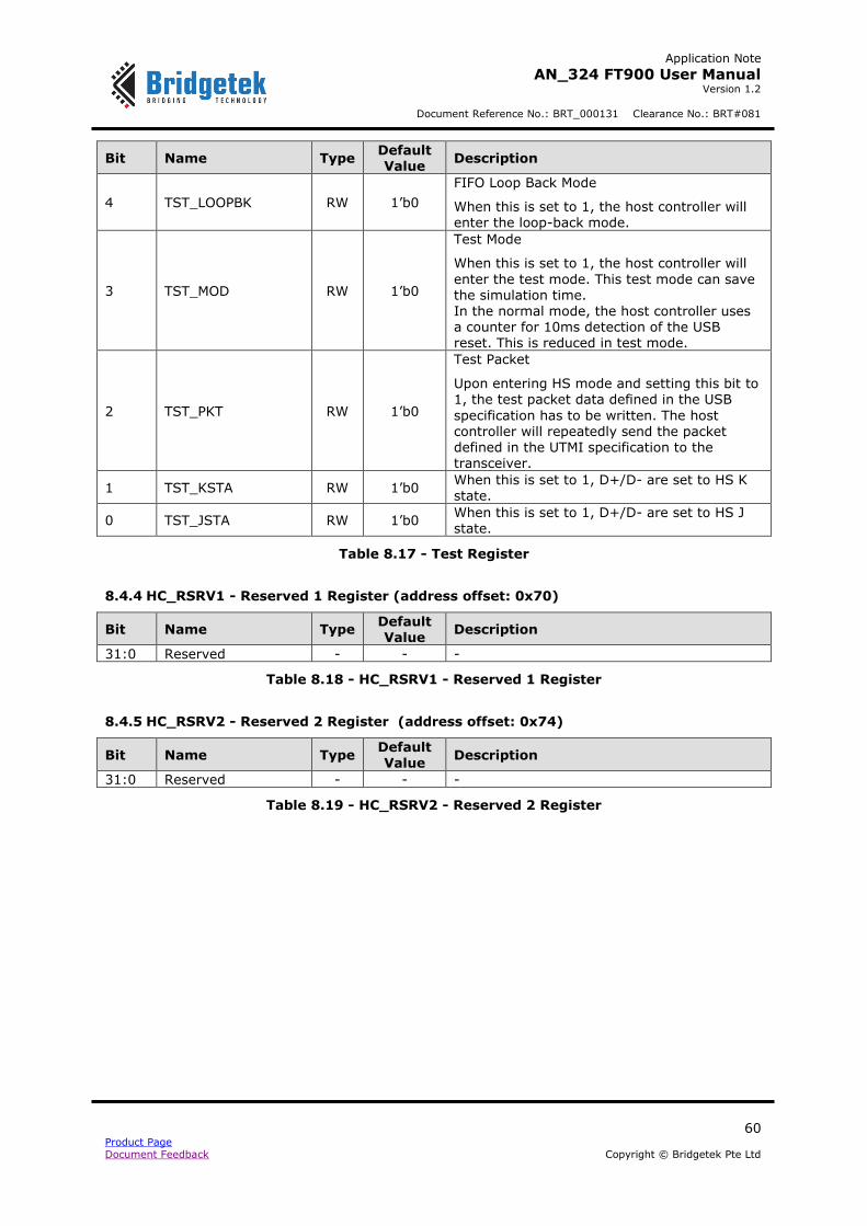
Application Note
AN_324 FT900 User Manual Version 1.2
Document Reference No.: BRT_000131 Clearance No.: BRT#081
60 Product Page Document Feedback Copyright © Bridgetek Pte Ltd
Bit Name Type Default Value
Description
4 TST_LOOPBK RW 1’b0
FIFO Loop Back Mode
When this is set to 1, the host controller will enter the loop-back mode.
3 TST_MOD RW 1’b0
Test Mode
When this is set to 1, the host controller will
enter the test mode. This test mode can save the simulation time. In the normal mode, the host controller uses a counter for 10ms detection of the USB reset. This is reduced in test mode.
2 TST_PKT RW 1’b0
Test Packet
Upon entering HS mode and setting this bit to 1, the test packet data defined in the USB
specification has to be written. The host controller will repeatedly send the packet defined in the UTMI specification to the transceiver.
1 TST_KSTA RW 1’b0 When this is set to 1, D+/D- are set to HS K state.
0 TST_JSTA RW 1’b0 When this is set to 1, D+/D- are set to HS J state.
Table 8.17 - Test Register
8.4.4 HC_RSRV1 - Reserved 1 Register (address offset: 0x70)
Bit Name Type Default Value
Description
31:0 Reserved - - -
Table 8.18 - HC_RSRV1 - Reserved 1 Register
8.4.5 HC_RSRV2 - Reserved 2 Register (address offset: 0x74)
Bit Name Type Default Value
Description
31:0 Reserved - - -
Table 8.19 - HC_RSRV2 - Reserved 2 Register

Application Note
AN_324 FT900 User Manual Version 1.2
Document Reference No.: BRT_000131 Clearance No.: BRT#081
61 Product Page Document Feedback Copyright © Bridgetek Pte Ltd
9 USB peripheral
This is a USB device controller fully compliant with the USB 2.0 specification. It supports a control end point - End Point 0 (EP0) - and up to 7 other End Points (EP1-7).
The EP0 control endpoint buffer size ranges from 8 to 64 bytes, configurable via software. EP1-7 support optional double buffering. The number of end points supported can be set by software, as well as their individual direction, type (Interrupt, Bulk, and Isochronous) and buffer size (8-1024 bytes). The total buffer size to be shared by all end points is 4 kB.
9.1 Register Summary
Listed below are the registers with their offset from the base address (0x10180). All registers and buffer locations can only be accessed via Byte (8-bit) mode.
Address
Offset
Register Default
value
References
Initialization Registers
0x18 DC_ADDRESS_ENABLE – Address Register 0x00 Section 9.2.1
0x10 DC_MODE – Mode Register 0x00 Section 9.2.2
0x08 DC_INT_ENABLE – Interrupt Enable Register 0x00 Section 9.2.3
0x0C DC_EP_INT_ENABLE – Endpoints Interrupt Enable Register
0x00 Section 9.2.4
Control Endpoint Data Flow Registers
0x1C DC_EP0_CONTROL – Endpoint 0 Control Register 0x00 Section 9.3.1
0x20 DC_EP0_STATUS – Endpoint 0 Status Register 0x00 Section 9.3.2
0x24 DC_EP0_BUFFER_LENGTH – Endpoint 0 Buffer Length Register
0x00 Section 9.3.3
0x28 DC_EP0_BUFFER – Endpoint 0 Buffer Register 0x00 Section 9.3.4
Other Endpoints Data Flow Registers
0x2C DC_EP1_CONTROL – Endpoint 1 Control Register 0x00 Section 9.4.1
0x30 DC_EP1_STATUS – Endpoint 1 Status Register 0x00 Section 9.4.2
0x34 DC_EP1_BUFFER_LENGTH_LSB – Endpoint 1 Buffer
Length LSB Register 0x00 Section 9.4.3
0x35 DC_EP1_BUFFER_LENGTH_MSB – Endpoint 1 Buffer
Length MSB Register 0x00 Section 9.4.4
0x38 DC_EP1_BUFFER – Endpoint 1 Buffer Register 0x00 Section 9.4.5
0x3C DC_EP2_CONTROL – Endpoint 2 Control Register 0x00 Section 9.4.1
0x40 DC_EP2_STATUS – Endpoint 2 Status Register 0x00 Section 9.4.2
0x44 DC_EP2_BUFFER_LENGTH_LSB – Endpoint 2 Buffer Length LSB Register
0x00 Section 9.4.3
0x45 DC_EP2_BUFFER_LENGTH_MSB – Endpoint 2 Buffer Length MSB Register
0x00 Section 9.4.4
0x48 DC_EP2_BUFFER – Endpoint 2 Buffer Register 0x00 Section 9.4.5
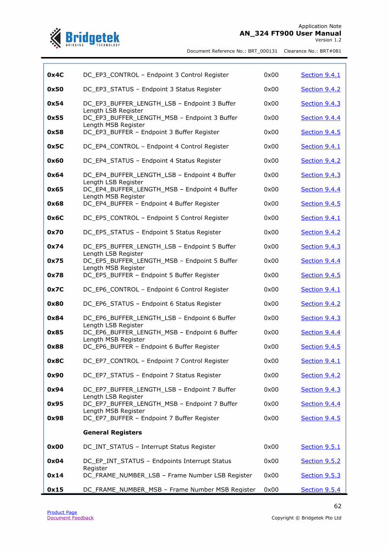
Application Note
AN_324 FT900 User Manual Version 1.2
Document Reference No.: BRT_000131 Clearance No.: BRT#081
62 Product Page Document Feedback Copyright © Bridgetek Pte Ltd
0x4C DC_EP3_CONTROL – Endpoint 3 Control Register 0x00 Section 9.4.1
0x50 DC_EP3_STATUS – Endpoint 3 Status Register 0x00 Section 9.4.2
0x54 DC_EP3_BUFFER_LENGTH_LSB – Endpoint 3 Buffer
Length LSB Register 0x00 Section 9.4.3
0x55 DC_EP3_BUFFER_LENGTH_MSB – Endpoint 3 Buffer
Length MSB Register 0x00 Section 9.4.4
0x58 DC_EP3_BUFFER – Endpoint 3 Buffer Register 0x00 Section 9.4.5
0x5C DC_EP4_CONTROL – Endpoint 4 Control Register 0x00 Section 9.4.1
0x60 DC_EP4_STATUS – Endpoint 4 Status Register 0x00 Section 9.4.2
0x64 DC_EP4_BUFFER_LENGTH_LSB – Endpoint 4 Buffer
Length LSB Register
0x00 Section 9.4.3
0x65 DC_EP4_BUFFER_LENGTH_MSB – Endpoint 4 Buffer
Length MSB Register 0x00 Section 9.4.4
0x68 DC_EP4_BUFFER – Endpoint 4 Buffer Register 0x00 Section 9.4.5
0x6C DC_EP5_CONTROL – Endpoint 5 Control Register 0x00 Section 9.4.1
0x70 DC_EP5_STATUS – Endpoint 5 Status Register 0x00 Section 9.4.2
0x74 DC_EP5_BUFFER_LENGTH_LSB – Endpoint 5 Buffer
Length LSB Register 0x00 Section 9.4.3
0x75 DC_EP5_BUFFER_LENGTH_MSB – Endpoint 5 Buffer
Length MSB Register 0x00 Section 9.4.4
0x78 DC_EP5_BUFFER – Endpoint 5 Buffer Register 0x00 Section 9.4.5
0x7C DC_EP6_CONTROL – Endpoint 6 Control Register 0x00 Section 9.4.1
0x80 DC_EP6_STATUS – Endpoint 6 Status Register 0x00 Section 9.4.2
0x84 DC_EP6_BUFFER_LENGTH_LSB – Endpoint 6 Buffer
Length LSB Register
0x00 Section 9.4.3
0x85 DC_EP6_BUFFER_LENGTH_MSB – Endpoint 6 Buffer
Length MSB Register 0x00 Section 9.4.4
0x88 DC_EP6_BUFFER – Endpoint 6 Buffer Register 0x00 Section 9.4.5
0x8C DC_EP7_CONTROL – Endpoint 7 Control Register 0x00 Section 9.4.1
0x90 DC_EP7_STATUS – Endpoint 7 Status Register 0x00 Section 9.4.2
0x94 DC_EP7_BUFFER_LENGTH_LSB – Endpoint 7 Buffer
Length LSB Register 0x00 Section 9.4.3
0x95 DC_EP7_BUFFER_LENGTH_MSB – Endpoint 7 Buffer
Length MSB Register 0x00 Section 9.4.4
0x98 DC_EP7_BUFFER – Endpoint 7 Buffer Register 0x00 Section 9.4.5
General Registers
0x00 DC_INT_STATUS – Interrupt Status Register 0x00 Section 9.5.1
0x04 DC_EP_INT_STATUS – Endpoints Interrupt Status
Register
0x00 Section 9.5.2
0x14 DC_FRAME_NUMBER_LSB – Frame Number LSB Register 0x00 Section 9.5.3
0x15 DC_FRAME_NUMBER_MSB – Frame Number MSB Register 0x00 Section 9.5.4

Application Note
AN_324 FT900 User Manual Version 1.2
Document Reference No.: BRT_000131 Clearance No.: BRT#081
63 Product Page Document Feedback Copyright © Bridgetek Pte Ltd
Table 9.1 - Overview of USB Peripheral Registers
9.2 Initialization Registers
9.2.1 DC_ADDRESS_ENABLE – Address Register (address offset: 0x18)
This register sets the USB assigned address sent from the USB host and enables the USB peripheral. In response to the standard USB request SET_ADDRESS, the firmware must write the peripheral address to this register.
Bit Name Type Default Value
Description
7 ENABLE RO 1’b0
Hardware sets this to 1 when software writes a new address to this register. It is cleared by
hardware at the end of the current transfer when the new address will take effect.
6:0 ADDR RW 7’h00 Function Address
Table 9.2 - DC_ADDRESS_ENABLE – Address Register
9.2.2 DC_MODE – Mode Register (address offset: 0x10)
This register allows the firmware to select the different test modes and enables the USB peripheral function.
Bit Name Type Default Value
Description
7 TST_MODE_ENABLE RW 1’b0 Test Mode Enable. Setting this to 1 to enter the test mode. It can only be cleared by hardware reset.
6:5 TST_MODE_SELECT RW 2’h0
Test Mode select (writeable only if MODE_ENABLE is 0)
2’h0: SE0_NAK 2’h1: J 2’h2: K 2’h3: Packet
4:2 Reserved - - -
1 FS_ONLY RW 1’b0 Setting this to 1 disables HS detection handshake
0 USB_DEV_EN RW 1’b0 USB function enables. Setting this to 1 enables the USB device
Table 9.3 - DC_MODE – Mode Register
9.2.3 DC_INT_ENABLE – Interrupt Enable Register (address offset: 0x08)
This register enables the different interrupt sources by writing a 1 to the corresponding bit.
Bit Name Type Default
Value Description
7 PHY_IE RW 1’b0 PHY receive error interrupt enable
6 PID_IE RW 1’b0 Package ID error interrupt enable
5 CRC16_IE RW 1’b0 CRC16 error interrupt enable
4 CRC5_IE RW 1’b0 CRC5 error interrupt enable
3 RESM_IE RW 1’b0 Resume interrupt enable
2 SUS_IE RW 1’b0 Suspend interrupt enable
1 RST_IE RW 1’b0 Reset interrupt enable
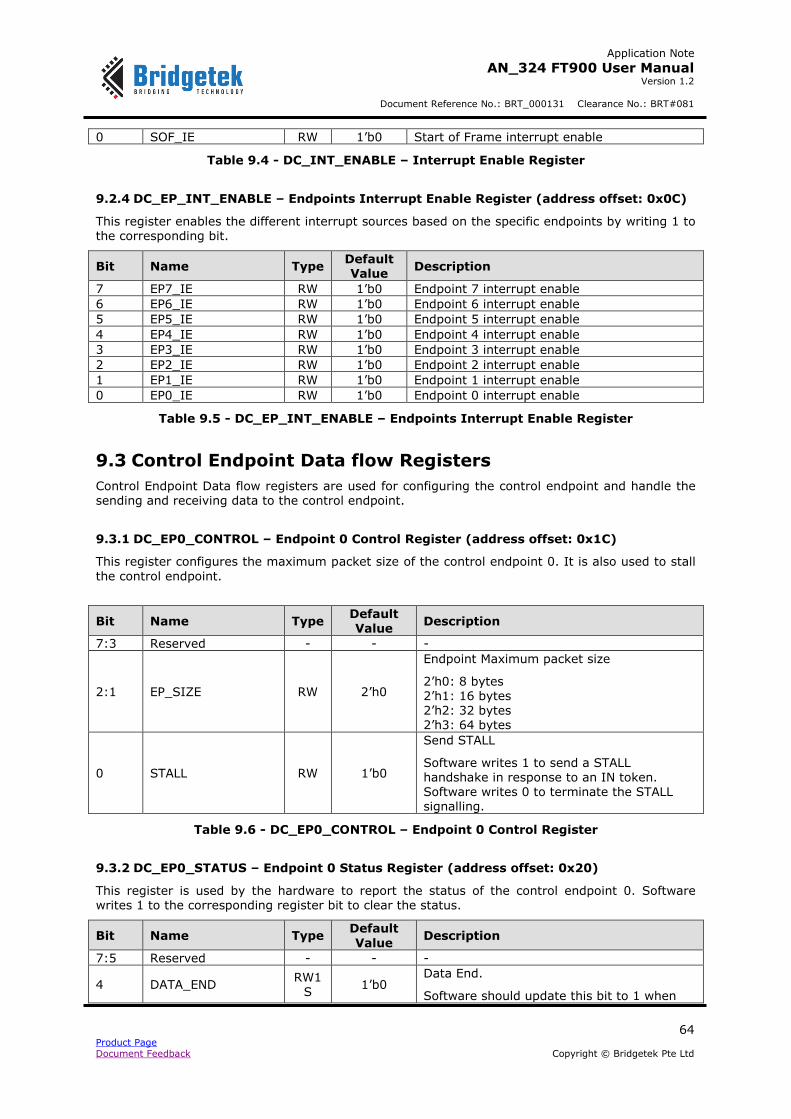
Application Note
AN_324 FT900 User Manual Version 1.2
Document Reference No.: BRT_000131 Clearance No.: BRT#081
64 Product Page Document Feedback Copyright © Bridgetek Pte Ltd
0 SOF_IE RW 1’b0 Start of Frame interrupt enable
Table 9.4 - DC_INT_ENABLE – Interrupt Enable Register
9.2.4 DC_EP_INT_ENABLE – Endpoints Interrupt Enable Register (address offset: 0x0C)
This register enables the different interrupt sources based on the specific endpoints by writing 1 to the corresponding bit.
Bit Name Type Default Value
Description
7 EP7_IE RW 1’b0 Endpoint 7 interrupt enable
6 EP6_IE RW 1’b0 Endpoint 6 interrupt enable
5 EP5_IE RW 1’b0 Endpoint 5 interrupt enable
4 EP4_IE RW 1’b0 Endpoint 4 interrupt enable
3 EP3_IE RW 1’b0 Endpoint 3 interrupt enable
2 EP2_IE RW 1’b0 Endpoint 2 interrupt enable
1 EP1_IE RW 1’b0 Endpoint 1 interrupt enable
0 EP0_IE RW 1’b0 Endpoint 0 interrupt enable
Table 9.5 - DC_EP_INT_ENABLE – Endpoints Interrupt Enable Register
9.3 Control Endpoint Data flow Registers
Control Endpoint Data flow registers are used for configuring the control endpoint and handle the sending and receiving data to the control endpoint.
9.3.1 DC_EP0_CONTROL – Endpoint 0 Control Register (address offset: 0x1C)
This register configures the maximum packet size of the control endpoint 0. It is also used to stall
the control endpoint.
Bit Name Type Default
Value Description
7:3 Reserved - - -
2:1 EP_SIZE RW 2’h0
Endpoint Maximum packet size
2’h0: 8 bytes 2’h1: 16 bytes 2’h2: 32 bytes 2’h3: 64 bytes
0 STALL RW 1’b0
Send STALL
Software writes 1 to send a STALL handshake in response to an IN token. Software writes 0 to terminate the STALL signalling.
Table 9.6 - DC_EP0_CONTROL – Endpoint 0 Control Register
9.3.2 DC_EP0_STATUS – Endpoint 0 Status Register (address offset: 0x20)
This register is used by the hardware to report the status of the control endpoint 0. Software writes 1 to the corresponding register bit to clear the status.
Bit Name Type Default
Value Description
7:5 Reserved - - -
4 DATA_END RW1
S 1’b0
Data End.
Software should update this bit to 1 when

Application Note
AN_324 FT900 User Manual Version 1.2
Document Reference No.: BRT_000131 Clearance No.: BRT#081
65 Product Page Document Feedback Copyright © Bridgetek Pte Ltd
writing: 1 to IN_PKT_RDY for last outgoing data
packet 1 to IN_PKT_RDY for a zero-length data
packet 1 to OUT_PKT_RDY after servicing the
last incoming data packet
3 STALL RW1
C 1’b0
Sent STALL.
Hardware sets this to 1 when the STALL
handshake has been transmitted. Software writes 1 to clear it.
2 SETUP RW1
C 1’b0
SETUP token received.
Hardware sets this to 1 and interrupts when the SETUP token has been received. Software writes 1 to clear it.
1 IN_PKT_RDY RW1
S 1’b0
IN packet ready.
Software should write 1 to it after loading a data packet into the endpoint 0 IN FIFO. Hardware clears it and generates an interrupt when the data packet has been
successfully transmitted.
0 OUT_PKT_RDY RW1
C 1’b0
OUT packet ready.
Hardware sets this bit to 1 and generates an interrupt when a data packet has been received. Software writes 1 to clear it after unloading the data packet from the endpoint
0 OUT FIFO.
Table 9.7 - DC_EP0_STATUS – Endpoint 0 Status Register
9.3.3 DC_EP0_BUFFER_LENGTH – Endpoint 0 Buffer Length Register (address offset:
0x24)
This register is used by the hardware to report the length of the packet received in the endpoint 0
OUT buffer.
Bit Name Type Default Value
Description
7 Reserved - - -
6:0 BUF_LEN RO 7’h00 Indicates the number of data bytes received. Valid only if OUT_PKT_RDY is 1.
Table 9.8 - DC_EP0_BUFFER_LENGTH – Endpoint 0 Buffer Length Register
9.3.4 DC_EP0_BUFFER – Endpoint 0 Buffer Register (address offset: 0x28)
This register is the used to access the endpoint 0 FIFO.
Bit Name Type Default Value
Description
7:0 Data R/W 8’h00
Endpoint 0 FIFO window register. A read unloads one data byte from the Endpoint 0 OUT FIFO. A write loads one data byte into
the Endpoint 0 IN FIFO.
Table 9.9 - DC_EP0_BUFFER – Endpoint 0 Buffer Register
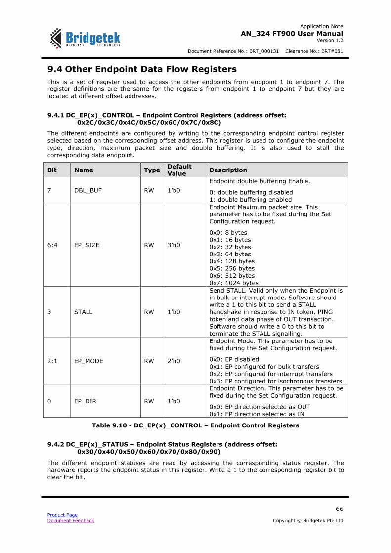
Application Note
AN_324 FT900 User Manual Version 1.2
Document Reference No.: BRT_000131 Clearance No.: BRT#081
66 Product Page Document Feedback Copyright © Bridgetek Pte Ltd
9.4 Other Endpoint Data Flow Registers
This is a set of register used to access the other endpoints from endpoint 1 to endpoint 7. The register definitions are the same for the registers from endpoint 1 to endpoint 7 but they are located at different offset addresses.
9.4.1 DC_EP(x)_CONTROL – Endpoint Control Registers (address offset: 0x2C/0x3C/0x4C/0x5C/0x6C/0x7C/0x8C)
The different endpoints are configured by writing to the corresponding endpoint control register selected based on the corresponding offset address. This register is used to configure the endpoint
type, direction, maximum packet size and double buffering. It is also used to stall the corresponding data endpoint.
Bit Name Type Default Value
Description
7 DBL_BUF RW 1’b0
Endpoint double buffering Enable.
0: double buffering disabled 1: double buffering enabled
6:4 EP_SIZE RW 3’h0
Endpoint Maximum packet size. This parameter has to be fixed during the Set Configuration request.
0x0: 8 bytes 0x1: 16 bytes 0x2: 32 bytes 0x3: 64 bytes 0x4: 128 bytes 0x5: 256 bytes 0x6: 512 bytes
0x7: 1024 bytes
3 STALL RW 1’b0
Send STALL. Valid only when the Endpoint is in bulk or interrupt mode. Software should write a 1 to this bit to send a STALL
handshake in response to IN token, PING
token and data phase of OUT transaction. Software should write a 0 to this bit to terminate the STALL signalling.
2:1 EP_MODE RW 2’h0
Endpoint Mode. This parameter has to be fixed during the Set Configuration request.
0x0: EP disabled
0x1: EP configured for bulk transfers 0x2: EP configured for interrupt transfers 0x3: EP configured for isochronous transfers
0 EP_DIR RW 1’b0
Endpoint Direction. This parameter has to be fixed during the Set Configuration request.
0x0: EP direction selected as OUT 0x1: EP direction selected as IN
Table 9.10 - DC_EP(x)_CONTROL – Endpoint Control Registers
9.4.2 DC_EP(x)_STATUS – Endpoint Status Registers (address offset:
0x30/0x40/0x50/0x60/0x70/0x80/0x90)
The different endpoint statuses are read by accessing the corresponding status register. The
hardware reports the endpoint status in this register. Write a 1 to the corresponding register bit to clear the bit.
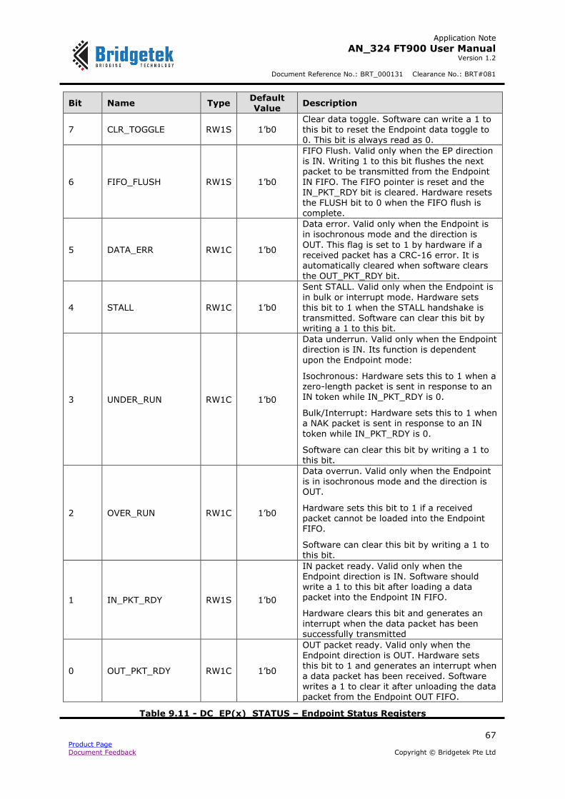
Application Note
AN_324 FT900 User Manual Version 1.2
Document Reference No.: BRT_000131 Clearance No.: BRT#081
67 Product Page Document Feedback Copyright © Bridgetek Pte Ltd
Bit Name Type Default Value
Description
7 CLR_TOGGLE RW1S 1’b0 Clear data toggle. Software can write a 1 to this bit to reset the Endpoint data toggle to 0. This bit is always read as 0.
6 FIFO_FLUSH RW1S 1’b0
FIFO Flush. Valid only when the EP direction is IN. Writing 1 to this bit flushes the next packet to be transmitted from the Endpoint
IN FIFO. The FIFO pointer is reset and the IN_PKT_RDY bit is cleared. Hardware resets the FLUSH bit to 0 when the FIFO flush is complete.
5 DATA_ERR RW1C 1’b0
Data error. Valid only when the Endpoint is in isochronous mode and the direction is
OUT. This flag is set to 1 by hardware if a received packet has a CRC-16 error. It is
automatically cleared when software clears the OUT_PKT_RDY bit.
4 STALL RW1C 1’b0
Sent STALL. Valid only when the Endpoint is
in bulk or interrupt mode. Hardware sets this bit to 1 when the STALL handshake is transmitted. Software can clear this bit by writing a 1 to this bit.
3 UNDER_RUN RW1C 1’b0
Data underrun. Valid only when the Endpoint direction is IN. Its function is dependent
upon the Endpoint mode:
Isochronous: Hardware sets this to 1 when a zero-length packet is sent in response to an IN token while IN_PKT_RDY is 0.
Bulk/Interrupt: Hardware sets this to 1 when a NAK packet is sent in response to an IN
token while IN_PKT_RDY is 0.
Software can clear this bit by writing a 1 to this bit.
2 OVER_RUN RW1C 1’b0
Data overrun. Valid only when the Endpoint is in isochronous mode and the direction is OUT.
Hardware sets this bit to 1 if a received packet cannot be loaded into the Endpoint FIFO.
Software can clear this bit by writing a 1 to this bit.
1 IN_PKT_RDY RW1S 1’b0
IN packet ready. Valid only when the Endpoint direction is IN. Software should write a 1 to this bit after loading a data packet into the Endpoint IN FIFO.
Hardware clears this bit and generates an
interrupt when the data packet has been successfully transmitted
0 OUT_PKT_RDY RW1C 1’b0
OUT packet ready. Valid only when the Endpoint direction is OUT. Hardware sets this bit to 1 and generates an interrupt when a data packet has been received. Software writes a 1 to clear it after unloading the data packet from the Endpoint OUT FIFO.
Table 9.11 - DC_EP(x)_STATUS – Endpoint Status Registers
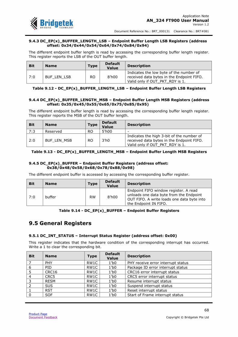
Application Note
AN_324 FT900 User Manual Version 1.2
Document Reference No.: BRT_000131 Clearance No.: BRT#081
68 Product Page Document Feedback Copyright © Bridgetek Pte Ltd
9.4.3 DC_EP(x)_BUFFER_LENGTH_LSB – Endpoint Buffer Length LSB Registers (address
offset: 0x34/0x44/0x54/0x64/0x74/0x84/0x94)
The different endpoint buffer length is read by accessing the corresponding buffer length register. This register reports the LSB of the OUT buffer length.
Bit Name Type Default Value
Description
7:0 BUF_LEN_LSB RO 8’h00 Indicates the low byte of the number of received data bytes in the Endpoint FIFO. Valid only if OUT_PKT_RDY is 1.
Table 9.12 - DC_EP(x)_BUFFER_LENGTH_LSB – Endpoint Buffer Length LSB Registers
9.4.4 DC_EP(x)_BUFFER_LENGTH_MSB – Endpoint Buffer Length MSB Registers (address
offset: 0x35/0x45/0x55/0x65/0x75/0x85/0x95)
The different endpoint buffer length is read by accessing the corresponding buffer length register.
This register reports the MSB of the OUT buffer length.
Bit Name Type Default Value
Description
7:3 Reserved RO 5’h00 -
2:0 BUF_LEN_MSB RO 3’h0
Indicates the high 3-bit of the number of
received data bytes in the Endpoint FIFO. Valid only if OUT_PKT_RDY is 1.
Table 9.13 - DC_EP(x)_BUFFER_LENGTH_MSB – Endpoint Buffer Length MSB Registers
9.4.5 DC_EP(x)_BUFFER – Endpoint Buffer Registers (address offset: 0x38/0x48/0x58/0x68/0x78/0x88/0x98)
The different endpoint buffer is accessed by accessing the corresponding buffer register.
Bit Name Type Default Value
Description
7:0 buffer RW 8’h00
Endpoint FIFO window register. A read unloads one data byte from the Endpoint
OUT FIFO. A write loads one data byte into the Endpoint IN FIFO.
Table 9.14 - DC_EP(x)_BUFFER – Endpoint Buffer Registers
9.5 General Registers
9.5.1 DC_INT_STATUS – Interrupt Status Register (address offset: 0x00)
This register indicates that the hardware condition of the corresponding interrupt has occurred. Write a 1 to clear the corresponding bit.
Bit Name Type Default
Value Description
7 PHY RW1C 1’b0 PHY receive error interrupt status
6 PID RW1C 1’b0 Package ID error interrupt status
5 CRC16 RW1C 1’b0 CRC16 error interrupt status
4 CRC5 RW1C 1’b0 CRC5 error interrupt status
3 RESM RW1C 1’b0 Resume interrupt status
2 SUS RW1C 1’b0 Suspend interrupt status
1 RST RW1C 1’b0 Reset interrupt status
0 SOF RW1C 1’b0 Start of Frame interrupt status

Application Note
AN_324 FT900 User Manual Version 1.2
Document Reference No.: BRT_000131 Clearance No.: BRT#081
69 Product Page Document Feedback Copyright © Bridgetek Pte Ltd
Table 9.15 - DC_INT_STATUS – Interrupt Status Register
9.5.2 DC_EP_INT_STATUS – Endpoints Interrupt Status Register (address offset: 0x04)
This register indicates the corresponding endpoint hardware condition has occurred. Write a 1 to clear the corresponding bit.
Bit Name Type Default Value
Description
7 EP7 RW1C 1’b0 Endpoint 7 interrupt status
6 EP6 RW1C 1’b0 Endpoint 6 interrupt status
5 EP5 RW1C 1’b0 Endpoint 5 interrupt status
4 EP4 RW1C 1’b0 Endpoint 4 interrupt status
3 EP3 RW1C 1’b0 Endpoint 3 interrupt status
2 EP2 RW1C 1’b0 Endpoint 2 interrupt status
1 EP1 RW1C 1’b0 Endpoint 1 interrupt status
0 EP0 RW1C 1’b0 Endpoint 0 interrupt status
Table 9.16 - DC_EP_INT_STATUS – Endpoints Interrupt Status Register
9.5.3 DC_FRAME_NUMBER_LSB – Frame Number LSB Register (address offset: 0x14)
This register has the LSB of the last successfully received SOF.
Bit Name Type Default Value
Description
7:0 FRAME_LSB RO 8’h00 Frame Number for last received SOF, Least significant byte
Table 9.17 - DC_FRAME_NUMBER_LSB – Frame Number LSB Register
9.5.4 DC_FRAME_NUMBER_MSB – Frame Number MSB Register (address offset: 0x15)
This register has the MSB of the last successfully received SOF.
Bit Name Type Default Value
Description
7:3 Reserved RO 5’h00 -
2:0 FRAME_MSB RO 3’h0 Frame Number for last received SOF, Most significant byte
Table 9.18 - DC_FRAME_NUMBER_MSB – Frame Number MSB Register
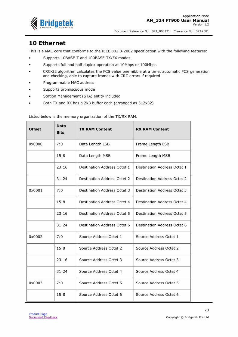
Application Note
AN_324 FT900 User Manual Version 1.2
Document Reference No.: BRT_000131 Clearance No.: BRT#081
70 Product Page Document Feedback Copyright © Bridgetek Pte Ltd
10 Ethernet
This is a MAC core that conforms to the IEEE 802.3-2002 specification with the following features:
• Supports 10BASE-T and 100BASE-TX/FX modes
• Supports full and half duplex operation at 10Mbps or 100Mbps
• CRC-32 algorithm calculates the FCS value one nibble at a time, automatic FCS generation and checking, able to capture frames with CRC errors if required
• Programmable MAC address
• Supports promiscuous mode
• Station Management (STA) entity included
• Both TX and RX has a 2kB buffer each (arranged as 512x32)
Listed below is the memory organization of the TX/RX RAM.
Offset Data
Bits TX RAM Content RX RAM Content
0x0000 7:0 Data Length LSB Frame Length LSB
15:8 Data Length MSB Frame Length MSB
23:16 Destination Address Octet 1 Destination Address Octet 1
31:24 Destination Address Octet 2 Destination Address Octet 2
0x0001 7:0 Destination Address Octet 3 Destination Address Octet 3
15:8 Destination Address Octet 4 Destination Address Octet 4
23:16 Destination Address Octet 5 Destination Address Octet 5
31:24 Destination Address Octet 6 Destination Address Octet 6
0x0002 7:0 Source Address Octet 1 Source Address Octet 1
15:8 Source Address Octet 2 Source Address Octet 2
23:16 Source Address Octet 3 Source Address Octet 3
31:24 Source Address Octet 4 Source Address Octet 4
0x0003 7:0 Source Address Octet 5 Source Address Octet 5
15:8 Source Address Octet 6 Source Address Octet 6

Application Note
AN_324 FT900 User Manual Version 1.2
Document Reference No.: BRT_000131 Clearance No.: BRT#081
71 Product Page Document Feedback Copyright © Bridgetek Pte Ltd
Offset Data
Bits TX RAM Content RX RAM Content
23:16 Type/Len MSB Type/Len MSB
31:24 Type/Len LSB Type/Len LSB
0x0004 –
0x01FF 7:0 Data octet n Data octet n
15:8 Data octet n+1 Data octet n+1
23:16 Data octet n+2 Data octet n+2
31:24 Data octet n+3 Data octet n+3
Table 10.1 - Memory Organization of TX/RX RAM
The memory is accessed indirectly using the data register. Data bits from the table above directly correspond to data bits of the Data Register. The TX RAM offset in the table above corresponds
directly to the RAM address. The RX RAM offset in the table above defines the distance from the beginning of the frame in the FIFO.
10.1 Register Summary
Listed below are the registers with their offset from the base address (0x10220). All registers and
buffer locations can only be accessed via Byte (8-bit), Word (16-bit) or Double-Word (32-bit).
However, the FIFO must be accessed in Double-Word mode only.
Address Offset
Register Default value
References
Ethernet Registers
0x00 ETH_INT_STATUS – Interrupt Status Register 0x00 Section 10.2.1
0x01 ETH_INT_ENABLE – Interrupt Enable Register 0x00 Section 10.2.2
0x02 ETH_RX_CNTL – Receive Control Register 0x00 Section 10.2.3
0x03 ETH_TX_CNTL – Transmit Control Register 0x00 Section 10.2.4
0x04 ETH_DATA – Data Register (octet n) 0x00 Section 10.2.5
0x05 ETH_DATA – Data Register (octet n+1) 0x00 Section 10.2.6
0x06 ETH_DATA – Data Register (octet n+2) 0x00 Section 10.2.7
0x07 ETH_DATA – Data Register (octet n+3) 0x00 Section 10.2.8
0x08 ETH_ADDR – Address Register (octet 1) 0x00 Section 10.2.9
0x09 ETH_ADDR – Address Register (octet 2) 0x00 Section 10.2.10
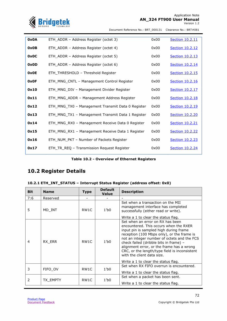
Application Note
AN_324 FT900 User Manual Version 1.2
Document Reference No.: BRT_000131 Clearance No.: BRT#081
72 Product Page Document Feedback Copyright © Bridgetek Pte Ltd
0x0A ETH_ADDR – Address Register (octet 3) 0x00 Section 10.2.11
0x0B ETH_ADDR – Address Register (octet 4) 0x00 Section 10.2.12
0x0C ETH_ADDR – Address Register (octet 5) 0x00 Section 10.2.13
0x0D ETH_ADDR – Address Register (octet 6) 0x00 Section 10.2.14
0x0E ETH_THRESHOLD – Threshold Register 0x00 Section 10.2.15
0x0F ETH_MNG_CNTL – Management Control Register 0x00 Section 10.2.16
0x10 ETH_MNG_DIV – Management Divider Register 0x00 Section 10.2.17
0x11 ETH_MNG_ADDR – Management Address Register 0x00 Section 10.2.18
0x12 ETH_MNG_TX0 – Management Transmit Data 0 Register 0x00 Section 10.2.19
0x13 ETH_MNG_TX1 – Management Transmit Data 1 Register 0x00 Section 10.2.20
0x14 ETH_MNG_RX0 – Management Receive Data 0 Register 0x00 Section 10.2.21
0x15 ETH_MNG_RX1 – Management Receive Data 1 Register 0x00 Section 10.2.22
0x16 ETH_NUM_PKT – Number of Packets Register 0x00 Section 10.2.23
0x17 ETH_TR_REQ – Transmission Request Register 0x00 Section 10.2.24
Table 10.2 - Overview of Ethernet Registers
10.2 Register Details
10.2.1 ETH_INT_STATUS – Interrupt Status Register (address offset: 0x0)
Bit Name Type Default Value
Description
7:6 Reserved - - -
5 MD_INT RW1C 1’b0
Set when a transaction on the MII management interface has completed successfully (either read or write).
Write a 1 to clear the status flag.
4 RX_ERR RW1C 1’b0
Set when an error on RX has been
encountered. This occurs when the RXER input pin is sampled high during frame reception (100 Mbps only), or the frame is not an integer number of octets and the FCS check failed (dribble bits in frame) – alignment error, or the frame has a wrong
CRC, or the length/type field is inconsistent
with the client data size.
Write a 1 to clear the status flag.
3 FIFO_OV RW1C 1’b0 Set when RX FIFO overrun is encountered.
Write a 1 to clear the status flag.
2 TX_EMPTY RW1C 1’b0 Set when a packet has been sent.
Write a 1 to clear the status flag.
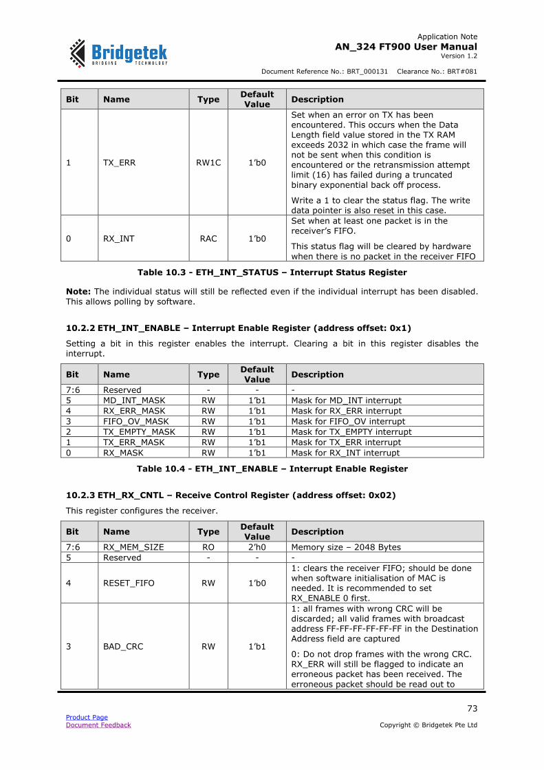
Application Note
AN_324 FT900 User Manual Version 1.2
Document Reference No.: BRT_000131 Clearance No.: BRT#081
73 Product Page Document Feedback Copyright © Bridgetek Pte Ltd
Bit Name Type Default Value
Description
1 TX_ERR RW1C 1’b0
Set when an error on TX has been encountered. This occurs when the Data Length field value stored in the TX RAM exceeds 2032 in which case the frame will not be sent when this condition is encountered or the retransmission attempt limit (16) has failed during a truncated
binary exponential back off process.
Write a 1 to clear the status flag. The write data pointer is also reset in this case.
0 RX_INT RAC 1’b0
Set when at least one packet is in the receiver’s FIFO.
This status flag will be cleared by hardware
when there is no packet in the receiver FIFO
Table 10.3 - ETH_INT_STATUS – Interrupt Status Register
Note: The individual status will still be reflected even if the individual interrupt has been disabled.
This allows polling by software.
10.2.2 ETH_INT_ENABLE – Interrupt Enable Register (address offset: 0x1)
Setting a bit in this register enables the interrupt. Clearing a bit in this register disables the interrupt.
Bit Name Type Default Value
Description
7:6 Reserved - - -
5 MD_INT_MASK RW 1’b1 Mask for MD_INT interrupt
4 RX_ERR_MASK RW 1’b1 Mask for RX_ERR interrupt
3 FIFO_OV_MASK RW 1’b1 Mask for FIFO_OV interrupt
2 TX_EMPTY_MASK RW 1’b1 Mask for TX_EMPTY interrupt
1 TX_ERR_MASK RW 1’b1 Mask for TX_ERR interrupt
0 RX_MASK RW 1’b1 Mask for RX_INT interrupt
Table 10.4 - ETH_INT_ENABLE – Interrupt Enable Register
10.2.3 ETH_RX_CNTL – Receive Control Register (address offset: 0x02)
This register configures the receiver.
Bit Name Type Default Value
Description
7:6 RX_MEM_SIZE RO 2’h0 Memory size – 2048 Bytes
5 Reserved - - -
4 RESET_FIFO RW 1’b0
1: clears the receiver FIFO; should be done when software initialisation of MAC is needed. It is recommended to set RX_ENABLE 0 first.
3 BAD_CRC RW 1’b1
1: all frames with wrong CRC will be discarded; all valid frames with broadcast address FF-FF-FF-FF-FF-FF in the Destination Address field are captured
0: Do not drop frames with the wrong CRC. RX_ERR will still be flagged to indicate an erroneous packet has been received. The
erroneous packet should be read out to

Application Note
AN_324 FT900 User Manual Version 1.2
Document Reference No.: BRT_000131 Clearance No.: BRT#081
74 Product Page Document Feedback Copyright © Bridgetek Pte Ltd
Bit Name Type Default Value
Description
make place for subsequent packets.
2 PRMS_MODE RW 1’b0
1: Promiscuous mode enabled; all valid frames regardless of destination address will be captured, including multicast and broadcast frames.
0: Promiscuous mode disabled
1 ACC_MULTI RW 1’b0 1: Accept multicast; accepts all frames which have first bit of Destination Address set.
0 RX_ENABLE RW 1’b0 1: enable frame receiver 0: disable frame receiver
Table 10.5 - ETH_RX_CNTL – Receive Control Register
10.2.4 ETH_TX_CNTL – Transmit Control Register (address offset: 0x03)
This register configures the transmitter.
Bit Name Type Default Value
Description
7:6 TX_MEM_SIZE RO 2’h0 Memory size – 2048 Bytes
5 Reserved - - -
4 DUPLEX_MODE RW 1’b0
1: enable duplex mode for Ethernet transmitter 0: disable duplex mode for Ethernet transmitter
3 Reserved - - -
2 CRC_ENABLE RW 1’b0 1: frames will be sent with CRC appended 0: frames will be sent without CRC appended
1 PAD_ENABLE RW 1’b0
1: padding will be appended to frames
shorter than the minimum frame size 0: padding will not be appended to frames shorter than the minimum frame size
0 TX_ENABLE RW 1’b0 1: enable transmitter 0: disable transmitter
Table 10.6 - ETH_TX_CNTL – Transmit Control Register
10.2.5 ETH_DATA_N0 – Data Register (octet n) (address offset: 0x04)
Bit Name Type Default Value
Description
7:0 DATA RW 8’h00 For read/write from/to data buffer (RX/TX RAM)
Table 10.7 - ETH_DATA_N0 – Data Register (octet n)
10.2.6 ETH_DATA_N1 – Data Register (octet n+1) (address offset: 0x05)
Bit Name Type Default
Value Description
7:0 DATA RW 8’h00 For read/write from/to data buffer (RX/TX RAM)
Table 10.8 - ETH_DATA_N1 – Data Register (octet n+1)
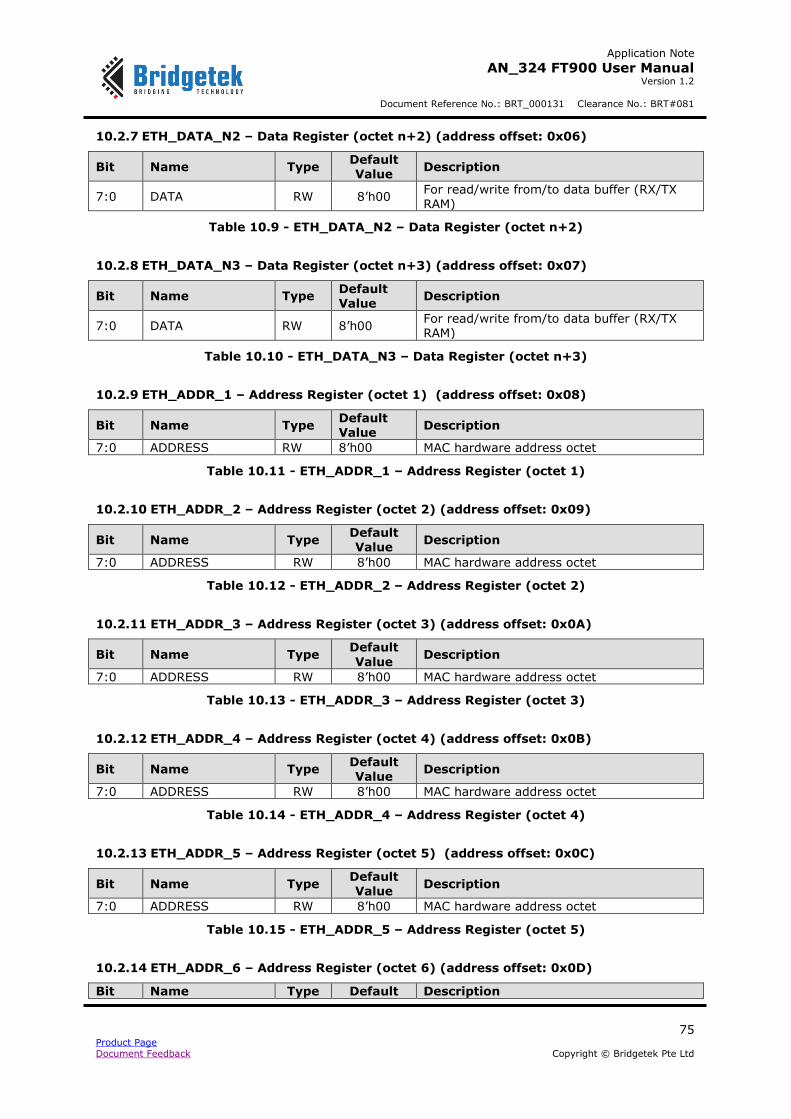
Application Note
AN_324 FT900 User Manual Version 1.2
Document Reference No.: BRT_000131 Clearance No.: BRT#081
75 Product Page Document Feedback Copyright © Bridgetek Pte Ltd
10.2.7 ETH_DATA_N2 – Data Register (octet n+2) (address offset: 0x06)
Bit Name Type Default Value
Description
7:0 DATA RW 8’h00 For read/write from/to data buffer (RX/TX RAM)
Table 10.9 - ETH_DATA_N2 – Data Register (octet n+2)
10.2.8 ETH_DATA_N3 – Data Register (octet n+3) (address offset: 0x07)
Bit Name Type Default Value
Description
7:0 DATA RW 8’h00 For read/write from/to data buffer (RX/TX RAM)
Table 10.10 - ETH_DATA_N3 – Data Register (octet n+3)
10.2.9 ETH_ADDR_1 – Address Register (octet 1) (address offset: 0x08)
Bit Name Type Default Value
Description
7:0 ADDRESS RW 8’h00 MAC hardware address octet
Table 10.11 - ETH_ADDR_1 – Address Register (octet 1)
10.2.10 ETH_ADDR_2 – Address Register (octet 2) (address offset: 0x09)
Bit Name Type Default Value
Description
7:0 ADDRESS RW 8’h00 MAC hardware address octet
Table 10.12 - ETH_ADDR_2 – Address Register (octet 2)
10.2.11 ETH_ADDR_3 – Address Register (octet 3) (address offset: 0x0A)
Bit Name Type Default
Value Description
7:0 ADDRESS RW 8’h00 MAC hardware address octet
Table 10.13 - ETH_ADDR_3 – Address Register (octet 3)
10.2.12 ETH_ADDR_4 – Address Register (octet 4) (address offset: 0x0B)
Bit Name Type Default Value
Description
7:0 ADDRESS RW 8’h00 MAC hardware address octet
Table 10.14 - ETH_ADDR_4 – Address Register (octet 4)
10.2.13 ETH_ADDR_5 – Address Register (octet 5) (address offset: 0x0C)
Bit Name Type Default Value
Description
7:0 ADDRESS RW 8’h00 MAC hardware address octet
Table 10.15 - ETH_ADDR_5 – Address Register (octet 5)
10.2.14 ETH_ADDR_6 – Address Register (octet 6) (address offset: 0x0D)
Bit Name Type Default Description
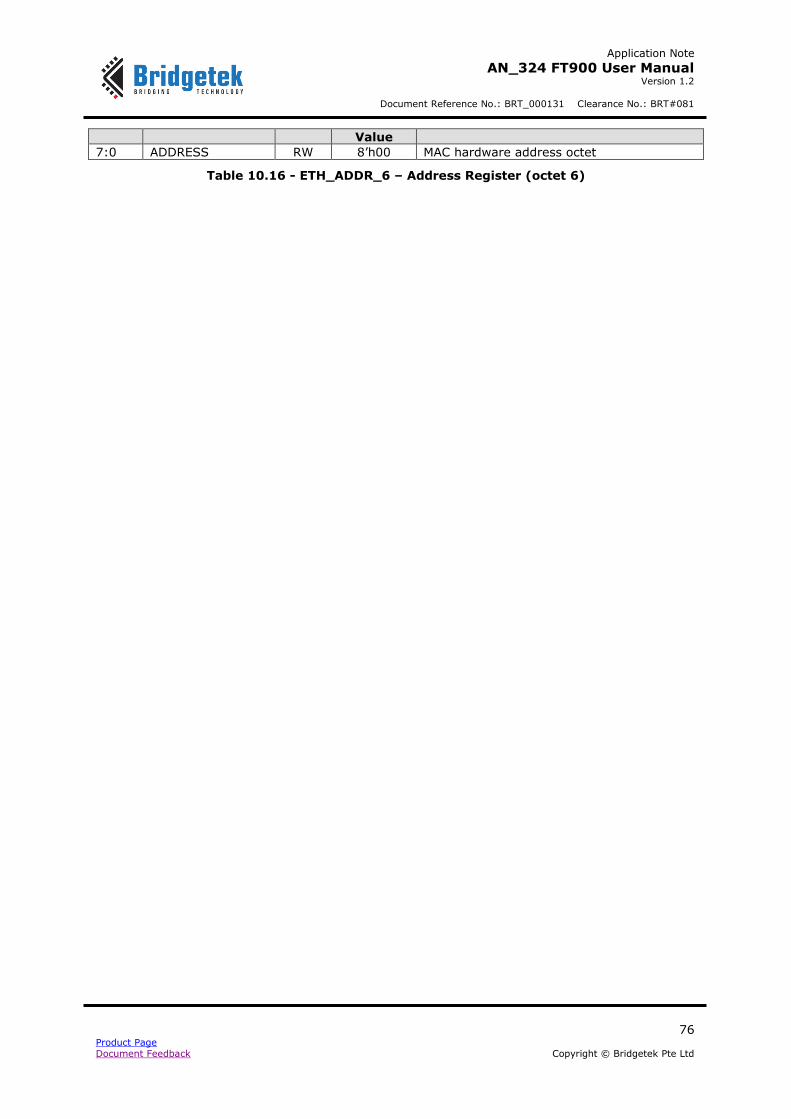
Application Note
AN_324 FT900 User Manual Version 1.2
Document Reference No.: BRT_000131 Clearance No.: BRT#081
76 Product Page Document Feedback Copyright © Bridgetek Pte Ltd
Value
7:0 ADDRESS RW 8’h00 MAC hardware address octet
Table 10.16 - ETH_ADDR_6 – Address Register (octet 6)

Application Note
AN_324 FT900 User Manual Version 1.2
Document Reference No.: BRT_000131 Clearance No.: BRT#081
77 Product Page Document Feedback Copyright © Bridgetek Pte Ltd
10.2.15 ETH_THRESHOLD – Threshold Register (address offset: 0x0E)
Bit Name Type Default Value
Description
7:6 Reserved - - -
5:0 THRESHOLD RW 6’h00
This threshold specifies the threshold level for the TX RAM to begin transmission. When the byte count of the data in the TX RAM reaches this level, the transmission will
start. Transmission starts when:
Number of bytes written >= 4 * (THRESHOLD * 8 + 1)
Table 10.17 - ETH_THRESHOLD – Threshold Register
10.2.16 ETH_MNG_CNTL – Management Control Register (address offset: 0x0F)
This register is used to send management frames from the STA entity across the MII management interface
Bit Name Type Default Value
Description
7:3 REG_ADDRESS RW 5’h00 These set the MII register address for the next transaction.
2 Reserved - - -
1 WRITE RW 1’b0
This bit should be updated together with the START bit.
1: perform write transaction
0: perform read transaction
0 START RW 1’b0 Setting this bit to 1 will initiate the transaction. Hardware clears this bit after
the transaction is complete.
Table 10.18 - ETH_MNG_CNTL – Management Control Register
10.2.17 ETH_MNG_DIV – Management Divider Register (address offset: 0x10)
Bit Name Type Default Value
Description
7:0 DIV RW 8’h80
This is used to set the clock divider for the
MDC clock used by the STA to clock transactions between PHY and MAC across the serial MII interface.
The MDC clock is derived as follows:
𝐹𝑚𝑑𝑐 =𝐹𝑐𝑙𝑘
2 ∗ (𝑀𝐷𝑉𝑅 + 1)
Table 10.19 - ETH_MNG_DIV – Management Divider Register
10.2.18 ETH_MNG_ADDR – Management Address Register (address offset: 0x11)
Bit Name Type Default Value
Description
7:5 Reserved - - -
4:0 PHY_ADDRESS RW 5’h00 This register should be updated with the PHY
address
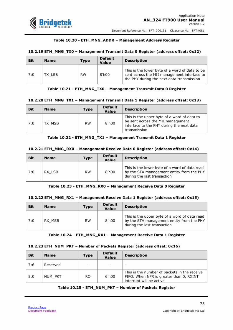
Application Note
AN_324 FT900 User Manual Version 1.2
Document Reference No.: BRT_000131 Clearance No.: BRT#081
78 Product Page Document Feedback Copyright © Bridgetek Pte Ltd
Table 10.20 - ETH_MNG_ADDR – Management Address Register
10.2.19 ETH_MNG_TX0 – Management Transmit Data 0 Register (address offset: 0x12)
Bit Name Type Default Value
Description
7:0 TX_LSB RW 8’h00 This is the lower byte of a word of data to be sent across the MII management interface to the PHY during the next data transmission
Table 10.21 - ETH_MNG_TX0 – Management Transmit Data 0 Register
10.2.20 ETH_MNG_TX1 – Management Transmit Data 1 Register (address offset: 0x13)
Bit Name Type Default
Value Description
7:0 TX_MSB RW 8’h00
This is the upper byte of a word of data to be sent across the MII management
interface to the PHY during the next data transmission
Table 10.22 - ETH_MNG_TX1 – Management Transmit Data 1 Register
10.2.21 ETH_MNG_RX0 – Management Receive Data 0 Register (address offset: 0x14)
Bit Name Type Default Value
Description
7:0 RX_LSB RW 8’h00 This is the lower byte of a word of data read by the STA management entity from the PHY during the last transaction
Table 10.23 - ETH_MNG_RX0 – Management Receive Data 0 Register
10.2.22 ETH_MNG_RX1 – Management Receive Data 1 Register (address offset: 0x15)
Bit Name Type Default Value
Description
7:0 RX_MSB RW 8’h00 This is the upper byte of a word of data read by the STA management entity from the PHY during the last transaction
Table 10.24 - ETH_MNG_RX1 – Management Receive Data 1 Register
10.2.23 ETH_NUM_PKT – Number of Packets Register (address offset: 0x16)
Bit Name Type Default
Value Description
7:6 Reserved - - -
5:0 NUM_PKT RO 6’h00 This is the number of packets in the receive FIFO. When NPR is greater than 0, RXINT interrupt will be active
Table 10.25 - ETH_NUM_PKT – Number of Packets Register

Application Note
AN_324 FT900 User Manual Version 1.2
Document Reference No.: BRT_000131 Clearance No.: BRT#081
79 Product Page Document Feedback Copyright © Bridgetek Pte Ltd
10.2.24 ETH_TR_REQ – Transmission Request Register (address offset: 0x17)
Bit Name Type Default Value
Description
7:1 Reserved - - -
0 NEW_TX RW1S 1’b0
1: Send the new frame in transmit memory.
Hardware clears this bit when the transmission is complete or an error on TX is
encountered.
Table 10.26 - ETH_TR_REQ – Transmission Request Register
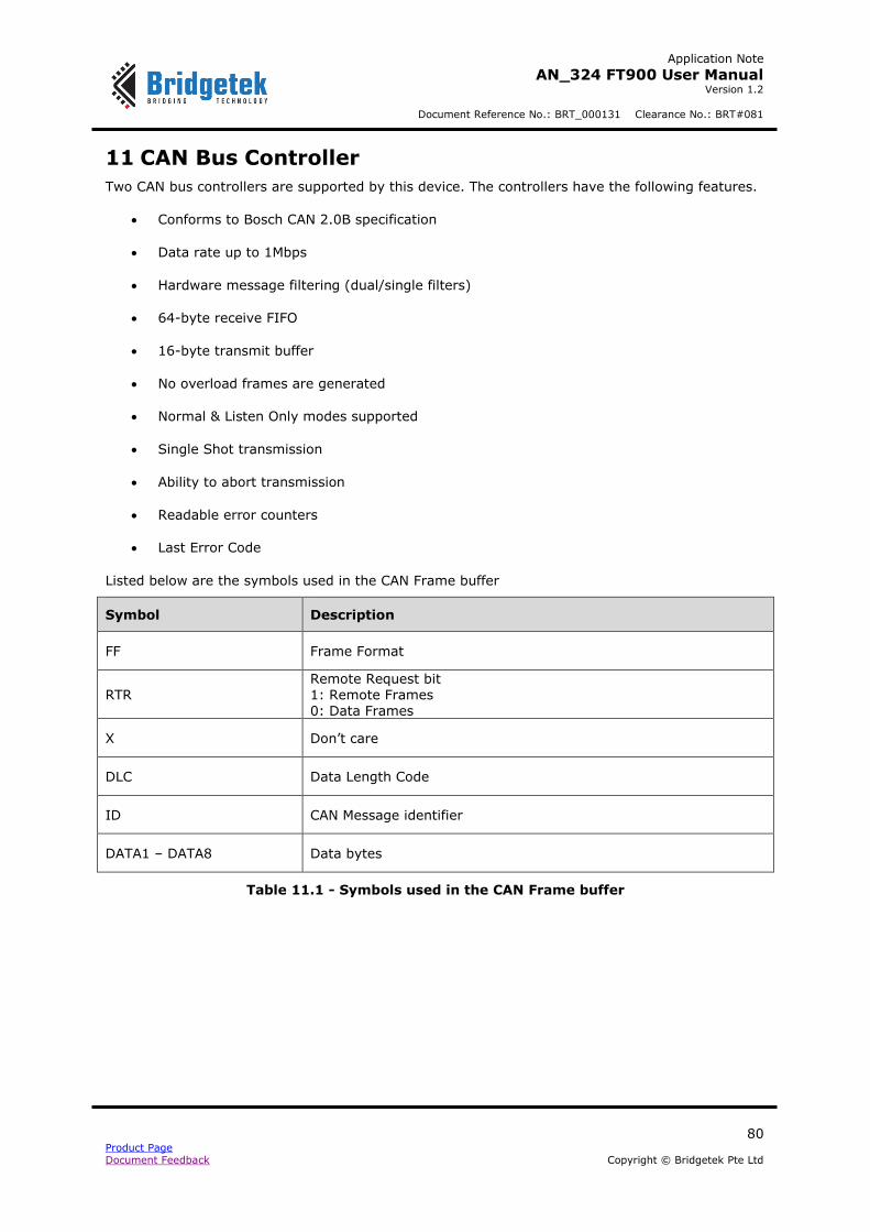
Application Note
AN_324 FT900 User Manual Version 1.2
Document Reference No.: BRT_000131 Clearance No.: BRT#081
80 Product Page Document Feedback Copyright © Bridgetek Pte Ltd
11 CAN Bus Controller
Two CAN bus controllers are supported by this device. The controllers have the following features.
Conforms to Bosch CAN 2.0B specification
Data rate up to 1Mbps
Hardware message filtering (dual/single filters)
64-byte receive FIFO
16-byte transmit buffer
No overload frames are generated
Normal & Listen Only modes supported
Single Shot transmission
Ability to abort transmission
Readable error counters
Last Error Code
Listed below are the symbols used in the CAN Frame buffer
Symbol Description
FF Frame Format
RTR
Remote Request bit
1: Remote Frames 0: Data Frames
X Don’t care
DLC Data Length Code
ID CAN Message identifier
DATA1 – DATA8 Data bytes
Table 11.1 - Symbols used in the CAN Frame buffer

Application Note
AN_324 FT900 User Manual Version 1.2
Document Reference No.: BRT_000131 Clearance No.: BRT#081
81 Product Page Document Feedback Copyright © Bridgetek Pte Ltd
The memory buffer layout for standard frames is:
Offset Data Bits Standard Frame buffer content for TX/RX RAM
0x00
7:0 FF RTR X/0 X/0 DLC3 DLC2 DLC1 DLC0
15:8 ID10 ID9 ID8 ID7 ID6 ID5 ID4 ID3
23:16 ID2 ID1 ID0 X/RTR X/0 X/0 X/0 X/0
31:24 DATA1
0x01
7:0 DATA2
15:8 DATA3
23:16 DATA4
31:24 DATA5
0x02
7:0 DATA6
15:8 DATA7
23:16 DATA8
31:24 UNUSED
0x03
7:0 UNUSED
15:8 UNUSED
23:16 UNUSED
31:24 UNUSED
Table 11.2 - Standard Frames Memory Buffer Layout
The memory buffer layout for extended frames is:
Offset Data Bits Extended Frame buffer content for TX/RX RAM
0x00
7:0 FF RTR X/0 X/0 DLC3 DLC2 DLC1 DLC0
15:8 ID28 ID27 ID26 ID25 ID24 ID23 ID22 ID21
23:16 ID20 ID19 ID18 ID17 ID16 ID15 ID14 ID13
31:24 ID12 ID11 ID10 ID9 ID8 ID7 ID6 ID5
0x01
7:0 ID4 ID3 ID2 ID1 ID0 X/RTR X/0 X/0
15:8 DATA1
23:16 DATA2
31:24 DATA3
0x02
7:0 DATA4
15:8 DATA5
23:16 DATA6
31:24 DATA7
0x03
7:0 DATA8
15:8 UNUSED
23:16 UNUSED
31:24 UNUSED
Table 11.3 - Extended Frames Memory Buffer Layout
11.1 Register Summary
Listed below are the registers with their offset from the base addresses (0x10240 for CAN1 and 0X10260 for CAN2). All registers and buffer locations can only be accessed via Byte (8-bit) mode.
Address
Offset
Register Default
value
References
0x00 CAN_MODE – Mode Register 0x04 Section 11.2.1
0x01 CAN_CMD – Command Register 0x00 Section 11.2.2
0x02 CAN_STATUS – Status Register 0x20 Section 11.2.3

Application Note
AN_324 FT900 User Manual Version 1.2
Document Reference No.: BRT_000131 Clearance No.: BRT#081
82 Product Page Document Feedback Copyright © Bridgetek Pte Ltd
0x03 CAN_INT_STATUS – Interrupt Status Register 0x00 Section 11.2.4
0x04 CAN_INT_ENABLE – Interrupt Enable Register 0x00 Section 11.2.5
0x05 CAN_RX_MSG – Receive Message Register 0x00 Section 11.2.6
0x06 CAN_BUS_TIM_0 – Bus Timing 0 Register 0x00 Section 11.2.7
0x07 CAN_BUS_TIM_1 – Bus Timing 1 Register 0x00 Section 11.2.8
0x08 CAN_TX_BUF_0 – Transmit Buffer 0 Register 0x00 Section 11.2.9.1
0x09 CAN_TX_BUF_1 – Transmit Buffer 1 Register 0x00 Section 11.2.9.2
0x0A CAN_TX_BUF_2 – Transmit Buffer 2 Register 0x00 Section 11.2.9.3
0x0B CAN_TX_BUF_3 – Transmit Buffer 3 Register 0x00 Section 11.2.9.4
0x0C CAN_RX_BUF_0 – Receive Buffer 0 Register 0x00 Section 11.2.10.1
0x0D CAN_RX_BUF_1 – Receive Buffer 1 Register 0x00 Section 11.2.10.2
0x0E CAN_RX_BUF_2 – Receive Buffer 2 Register 0x00 Section 11.2.10.3
0x0F CAN_RX_BUF_3 – Receive Buffer 3 Register 0x00 Section 11.2.10.4
0x10 CAN_ACC_CODE_0 – Acceptance Code 0 Register 0x00 Section 11.2.11.1
0x11 CAN_ACC_CODE_1 – Acceptance Code 1 Register 0x00 Section 11.2.11.2
0x12 CAN_ACC_CODE_2 – Acceptance Code 2 Register 0x00 Section 11.2.11.3
0x13 CAN_ACC_CODE_3 – Acceptance Code 3 Register 0x00 Section 11.2.11.4
0x14 CAN_ACC_MASK_0 – Acceptance Mask 0 Register 0x00 Section 11.2.11.5
0x15 CAN_ACC_MASK_1 – Acceptance Mask 1 Register 0x00 Section 11.2.11.6
0x16 CAN_ACC_MASK_2 – Acceptance Mask 2 Register 0x00 Section 11.2.11.7
0x17 CAN_ACC_MASK_3 – Acceptance Mask 3 Register 0x00 Section 11.2.11.8
0x18 CAN_ERR_CODE – Error Code Capture Register 0x00 Section 11.2.12
0x19 CAN_RX_ERR_CNTR – Receive Error Counter Register
0x00 Section 11.2.13
0x1A CAN_TX_ERR_CNTR – Transmit Error Counter Register
0x00 Section 11.2.14
0x1B CAN_ARB_LOST_CODE – Arbitration Lost Code
Capture Register
0x00 Section 11.2.15
Table 11.4 - Overview of CAN Registers
11.2 Register Details
11.2.1 CAN_MODE – Mode Register (address offset: 0x00)
Bit Name Type Default Value
Description
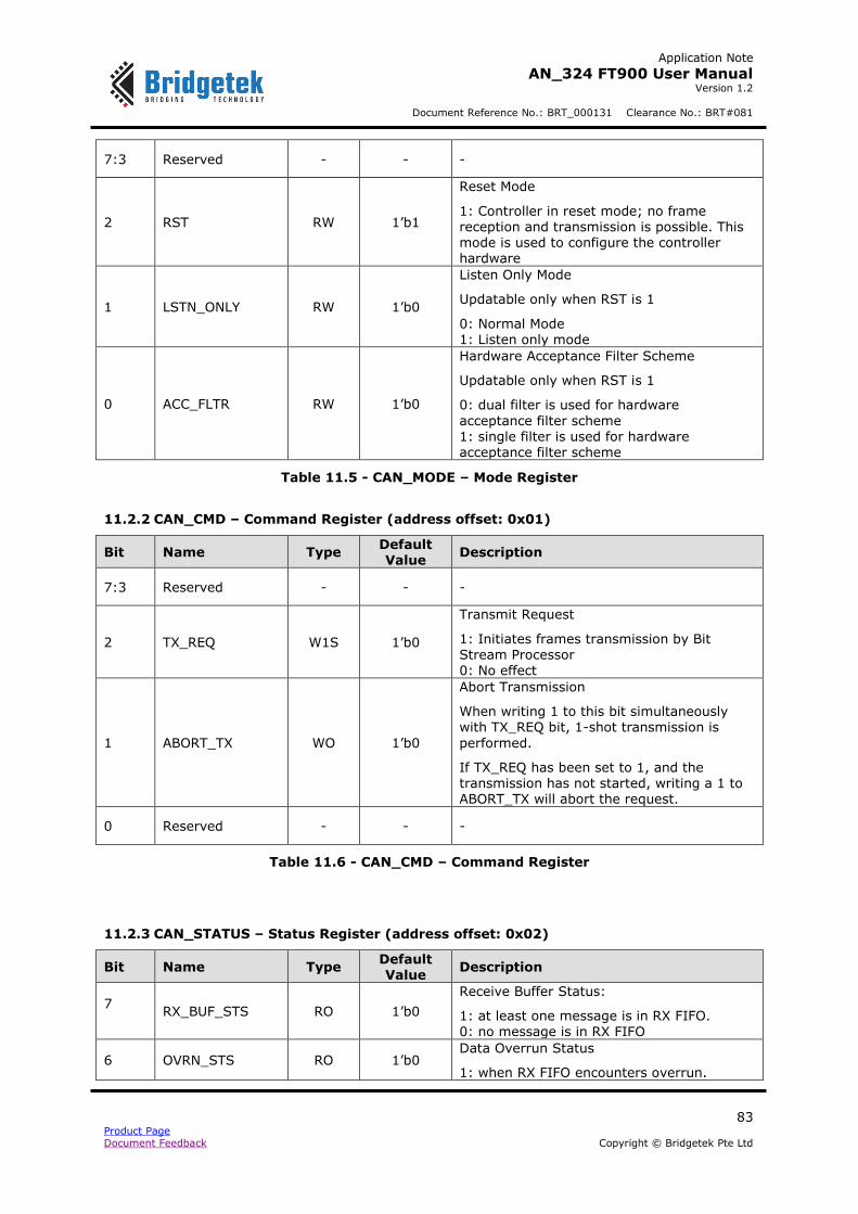
Application Note
AN_324 FT900 User Manual Version 1.2
Document Reference No.: BRT_000131 Clearance No.: BRT#081
83 Product Page Document Feedback Copyright © Bridgetek Pte Ltd
7:3 Reserved - - -
2 RST RW 1’b1
Reset Mode
1: Controller in reset mode; no frame reception and transmission is possible. This mode is used to configure the controller hardware
1 LSTN_ONLY RW 1’b0
Listen Only Mode
Updatable only when RST is 1
0: Normal Mode 1: Listen only mode
0 ACC_FLTR RW 1’b0
Hardware Acceptance Filter Scheme
Updatable only when RST is 1
0: dual filter is used for hardware
acceptance filter scheme 1: single filter is used for hardware acceptance filter scheme
Table 11.5 - CAN_MODE – Mode Register
11.2.2 CAN_CMD – Command Register (address offset: 0x01)
Bit Name Type Default Value
Description
7:3 Reserved - - -
2 TX_REQ W1S 1’b0
Transmit Request
1: Initiates frames transmission by Bit Stream Processor 0: No effect
1 ABORT_TX WO 1’b0
Abort Transmission
When writing 1 to this bit simultaneously with TX_REQ bit, 1-shot transmission is
performed.
If TX_REQ has been set to 1, and the transmission has not started, writing a 1 to ABORT_TX will abort the request.
0 Reserved - - -
Table 11.6 - CAN_CMD – Command Register
11.2.3 CAN_STATUS – Status Register (address offset: 0x02)
Bit Name Type Default Value
Description
7
RX_BUF_STS RO 1’b0
Receive Buffer Status:
1: at least one message is in RX FIFO. 0: no message is in RX FIFO
6 OVRN_STS RO 1’b0 Data Overrun Status
1: when RX FIFO encounters overrun.
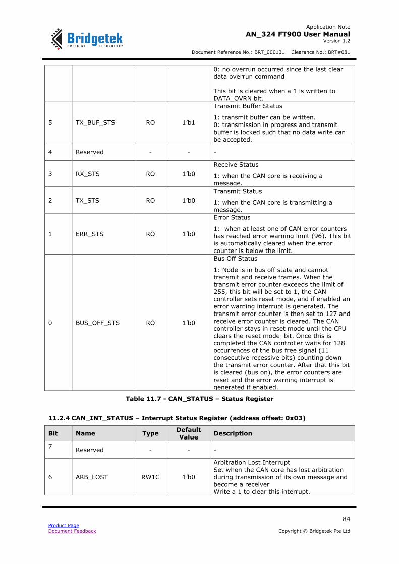
Application Note
AN_324 FT900 User Manual Version 1.2
Document Reference No.: BRT_000131 Clearance No.: BRT#081
84 Product Page Document Feedback Copyright © Bridgetek Pte Ltd
0: no overrun occurred since the last clear data overrun command This bit is cleared when a 1 is written to
DATA_OVRN bit.
5 TX_BUF_STS RO 1’b1
Transmit Buffer Status
1: transmit buffer can be written. 0: transmission in progress and transmit buffer is locked such that no data write can
be accepted.
4 Reserved - - -
3 RX_STS RO 1’b0
Receive Status
1: when the CAN core is receiving a
message.
2 TX_STS RO 1’b0
Transmit Status
1: when the CAN core is transmitting a message.
1 ERR_STS RO 1’b0
Error Status
1: when at least one of CAN error counters has reached error warning limit (96). This bit is automatically cleared when the error counter is below the limit.
0 BUS_OFF_STS RO 1’b0
Bus Off Status
1: Node is in bus off state and cannot transmit and receive frames. When the transmit error counter exceeds the limit of 255, this bit will be set to 1, the CAN controller sets reset mode, and if enabled an error warning interrupt is generated. The
transmit error counter is then set to 127 and
receive error counter is cleared. The CAN controller stays in reset mode until the CPU clears the reset mode bit. Once this is completed the CAN controller waits for 128 occurrences of the bus free signal (11 consecutive recessive bits) counting down the transmit error counter. After that this bit
is cleared (bus on), the error counters are reset and the error warning interrupt is generated if enabled.
Table 11.7 - CAN_STATUS – Status Register
11.2.4 CAN_INT_STATUS – Interrupt Status Register (address offset: 0x03)
Bit Name Type Default Value
Description
7
Reserved - - -
6 ARB_LOST RW1C 1’b0
Arbitration Lost Interrupt
Set when the CAN core has lost arbitration during transmission of its own message and become a receiver Write a 1 to clear this interrupt.
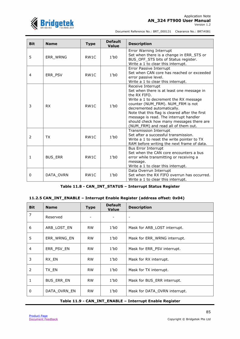
Application Note
AN_324 FT900 User Manual Version 1.2
Document Reference No.: BRT_000131 Clearance No.: BRT#081
85 Product Page Document Feedback Copyright © Bridgetek Pte Ltd
Bit Name Type Default Value
Description
5 ERR_WRNG RW1C 1’b0
Error Warning Interrupt Set when there is a change in ERR_STS or BUS_OFF_STS bits of Status register. Write a 1 to clear this interrupt.
4 ERR_PSV RW1C 1’b0
Error Passive Interrupt Set when CAN core has reached or exceeded
error passive level. Write a 1 to clear this interrupt.
3 RX RW1C 1’b0
Receive Interrupt Set when there is at least one message in the RX FIFO. Write a 1 to decrement the RX message
counter (NUM_FRM). NUM_FRM is not decremented automatically.
Note that this flag is cleared after the first message is read. The interrupt handler should check how many messages there are (NUM_FRM) and read all of them out.
2 TX RW1C 1’b0
Transmission Interrupt Set after a successful transmission. Write a 1 to reset the write pointer to TX RAM before writing the next frame of data.
1 BUS_ERR RW1C 1’b0
Bus Error Interrupt
Set when the CAN core encounters a bus error while transmitting or receiving a message. Write a 1 to clear this interrupt.
0 DATA_OVRN RW1C 1’b0
Data Overrun Interrupt
Set when the RX FIFO overrun has occurred. Write a 1 to clear this interrupt.
Table 11.8 - CAN_INT_STATUS – Interrupt Status Register
11.2.5 CAN_INT_ENABLE – Interrupt Enable Register (address offset: 0x04)
Bit Name Type Default
Value Description
7
Reserved - - -
6 ARB_LOST_EN RW 1’b0 Mask for ARB_LOST interrupt.
5 ERR_WRNG_EN RW 1’b0 Mask for ERR_WRNG interrupt.
4 ERR_PSV_EN RW 1’b0 Mask for ERR_PSV interrupt.
3 RX_EN RW 1’b0 Mask for RX interrupt.
2 TX_EN RW 1’b0 Mask for TX interrupt.
1 BUS_ERR_EN RW 1’b0 Mask for BUS_ERR interrupt.
0 DATA_OVRN_EN RW 1’b0 Mask for DATA_OVRN interrupt.
Table 11.9 - CAN_INT_ENABLE – Interrupt Enable Register
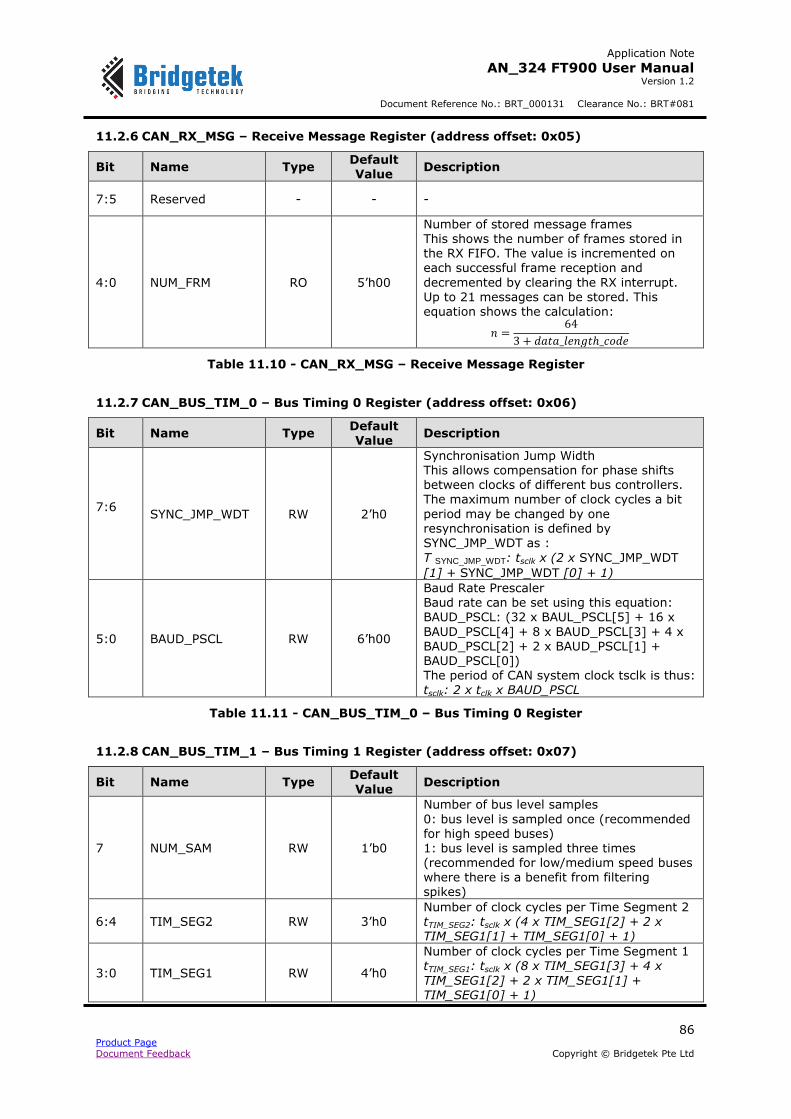
Application Note
AN_324 FT900 User Manual Version 1.2
Document Reference No.: BRT_000131 Clearance No.: BRT#081
86 Product Page Document Feedback Copyright © Bridgetek Pte Ltd
11.2.6 CAN_RX_MSG – Receive Message Register (address offset: 0x05)
Bit Name Type Default Value
Description
7:5 Reserved - - -
4:0 NUM_FRM RO 5’h00
Number of stored message frames This shows the number of frames stored in the RX FIFO. The value is incremented on each successful frame reception and
decremented by clearing the RX interrupt. Up to 21 messages can be stored. This equation shows the calculation:
𝑛 =64
3 + 𝑑𝑎𝑡𝑎_𝑙𝑒𝑛𝑔𝑡ℎ_𝑐𝑜𝑑𝑒
Table 11.10 - CAN_RX_MSG – Receive Message Register
11.2.7 CAN_BUS_TIM_0 – Bus Timing 0 Register (address offset: 0x06)
Bit Name Type Default Value
Description
7:6
SYNC_JMP_WDT RW 2’h0
Synchronisation Jump Width This allows compensation for phase shifts between clocks of different bus controllers. The maximum number of clock cycles a bit
period may be changed by one resynchronisation is defined by SYNC_JMP_WDT as :
T SYNC_JMP_WDT: tsclk x (2 x SYNC_JMP_WDT
[1] + SYNC_JMP_WDT [0] + 1)
5:0 BAUD_PSCL RW 6’h00
Baud Rate Prescaler Baud rate can be set using this equation: BAUD_PSCL: (32 x BAUL_PSCL[5] + 16 x
BAUD_PSCL[4] + 8 x BAUD_PSCL[3] + 4 x BAUD_PSCL[2] + 2 x BAUD_PSCL[1] + BAUD_PSCL[0]) The period of CAN system clock tsclk is thus: tsclk: 2 x tclk x BAUD_PSCL
Table 11.11 - CAN_BUS_TIM_0 – Bus Timing 0 Register
11.2.8 CAN_BUS_TIM_1 – Bus Timing 1 Register (address offset: 0x07)
Bit Name Type Default Value
Description
7 NUM_SAM RW 1’b0
Number of bus level samples
0: bus level is sampled once (recommended for high speed buses) 1: bus level is sampled three times (recommended for low/medium speed buses
where there is a benefit from filtering spikes)
6:4 TIM_SEG2 RW 3’h0 Number of clock cycles per Time Segment 2 tTIM_SEG2: tsclk x (4 x TIM_SEG1[2] + 2 x TIM_SEG1[1] + TIM_SEG1[0] + 1)
3:0 TIM_SEG1 RW 4’h0
Number of clock cycles per Time Segment 1 tTIM_SEG1: tsclk x (8 x TIM_SEG1[3] + 4 x
TIM_SEG1[2] + 2 x TIM_SEG1[1] + TIM_SEG1[0] + 1)
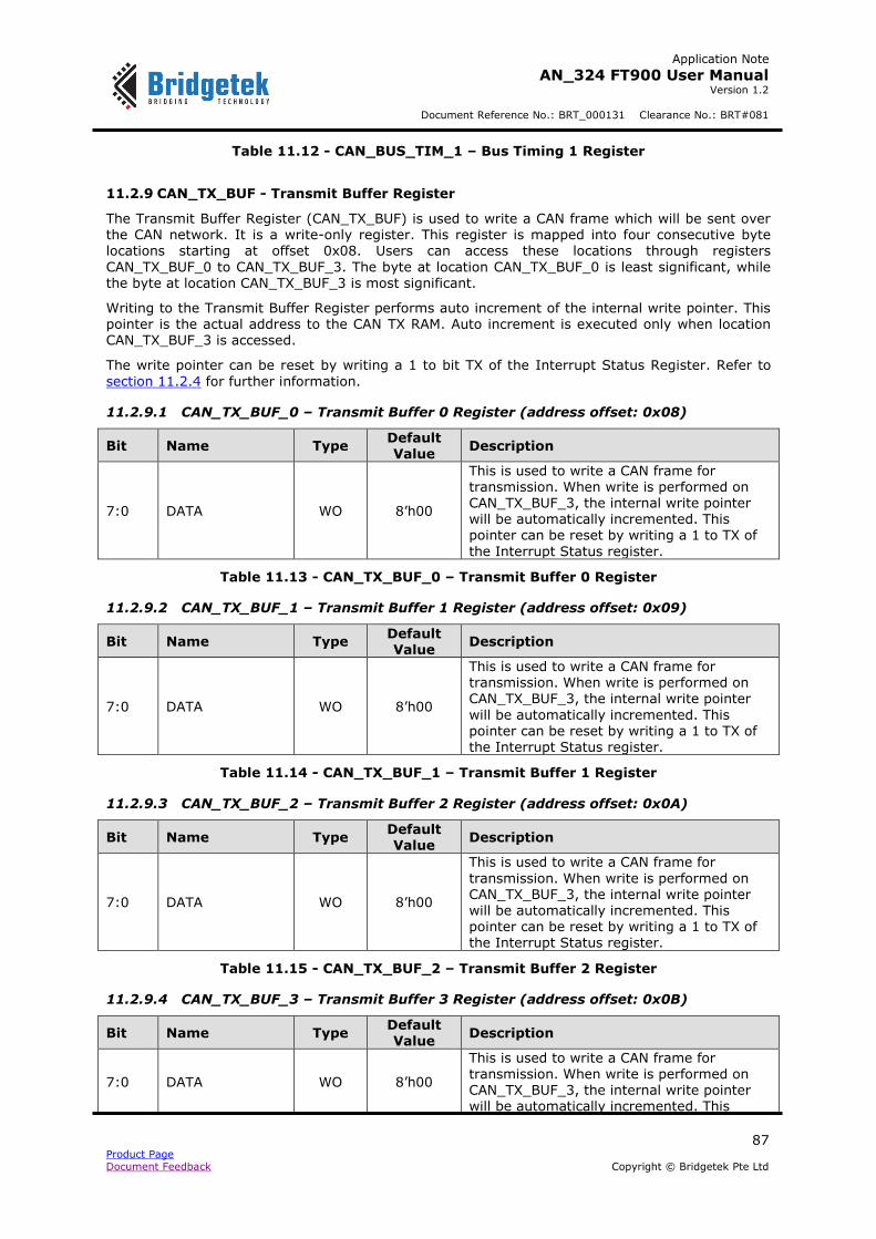
Application Note
AN_324 FT900 User Manual Version 1.2
Document Reference No.: BRT_000131 Clearance No.: BRT#081
87 Product Page Document Feedback Copyright © Bridgetek Pte Ltd
Table 11.12 - CAN_BUS_TIM_1 – Bus Timing 1 Register
11.2.9 CAN_TX_BUF - Transmit Buffer Register
The Transmit Buffer Register (CAN_TX_BUF) is used to write a CAN frame which will be sent over the CAN network. It is a write-only register. This register is mapped into four consecutive byte locations starting at offset 0x08. Users can access these locations through registers
CAN_TX_BUF_0 to CAN_TX_BUF_3. The byte at location CAN_TX_BUF_0 is least significant, while the byte at location CAN_TX_BUF_3 is most significant.
Writing to the Transmit Buffer Register performs auto increment of the internal write pointer. This pointer is the actual address to the CAN TX RAM. Auto increment is executed only when location CAN_TX_BUF_3 is accessed.
The write pointer can be reset by writing a 1 to bit TX of the Interrupt Status Register. Refer to
section 11.2.4 for further information.
11.2.9.1 CAN_TX_BUF_0 – Transmit Buffer 0 Register (address offset: 0x08)
Bit Name Type Default Value
Description
7:0 DATA WO 8’h00
This is used to write a CAN frame for transmission. When write is performed on CAN_TX_BUF_3, the internal write pointer will be automatically incremented. This pointer can be reset by writing a 1 to TX of
the Interrupt Status register.
Table 11.13 - CAN_TX_BUF_0 – Transmit Buffer 0 Register
11.2.9.2 CAN_TX_BUF_1 – Transmit Buffer 1 Register (address offset: 0x09)
Bit Name Type Default Value
Description
7:0 DATA WO 8’h00
This is used to write a CAN frame for transmission. When write is performed on
CAN_TX_BUF_3, the internal write pointer
will be automatically incremented. This pointer can be reset by writing a 1 to TX of the Interrupt Status register.
Table 11.14 - CAN_TX_BUF_1 – Transmit Buffer 1 Register
11.2.9.3 CAN_TX_BUF_2 – Transmit Buffer 2 Register (address offset: 0x0A)
Bit Name Type Default Value
Description
7:0 DATA WO 8’h00
This is used to write a CAN frame for
transmission. When write is performed on CAN_TX_BUF_3, the internal write pointer will be automatically incremented. This pointer can be reset by writing a 1 to TX of the Interrupt Status register.
Table 11.15 - CAN_TX_BUF_2 – Transmit Buffer 2 Register
11.2.9.4 CAN_TX_BUF_3 – Transmit Buffer 3 Register (address offset: 0x0B)
Bit Name Type Default Value
Description
7:0 DATA WO 8’h00
This is used to write a CAN frame for transmission. When write is performed on CAN_TX_BUF_3, the internal write pointer will be automatically incremented. This

Application Note
AN_324 FT900 User Manual Version 1.2
Document Reference No.: BRT_000131 Clearance No.: BRT#081
88 Product Page Document Feedback Copyright © Bridgetek Pte Ltd
pointer can be reset by writing a 1 to TX of the Interrupt Status register.
Table 11.16 - CAN_TX_BUF_3 – Transmit Buffer 3 Register
11.2.10 CAN_RX_BUF - Receive Buffer Register
The Receive Buffer Register (CAN_RX_BUF) is used to read CAN frames received from the CAN network. It is a read-only register. This register is mapped into four consecutive byte locations starting at offset 0x0C. The users can access these locations through registers CAN_RX_BUF_0 to CAN_RX_BUF_3. The byte at location CAN_RX_BUF_0 is least significant, while the byte at location CAN_RX_BUF_3 is most significant.
Reading the Receive Buffer Register performs auto increment of the internal read pointer. This
pointer is the actual address to the CAN RX FIFO. Auto increment is executed only when location CAN_RX_BUF_3 is accessed.
11.2.10.1 CAN_RX_BUF_0 – Receive Buffer 0 Register (address offset: 0x0C)
Bit Name Type Default Value
Description
7:0 DATA RO 8’h00
This is used to read a received CAN frame. When read is performed on CAN_RX_BUF_3, the internal read pointer will be automatically incremented.
Table 11.17 - CAN_RX_BUF_0 – Receive Buffer 0 Register
11.2.10.2 CAN_RX_BUF_1 – Receive Buffer 1 Register (address offset: 0x0D)
Bit Name Type Default Value
Description
7:0 DATA RO 8’h00
This is used to read a received CAN frame. When read is performed on CAN_RX_BUF_3, the internal read pointer will be
automatically incremented.
Table 11.18 - CAN_RX_BUF_1 – Receive Buffer 1 Register
11.2.10.3 CAN_RX_BUF_2 – Receive Buffer 2 Register (address offset: 0x0E)
Bit Name Type Default Value
Description
7:0 DATA RO 8’h00
This is used to read a received CAN frame. When read is performed on CAN_RX_BUF_3, the internal read pointer will be
automatically incremented.
Table 11.19 - CAN_RX_BUF_2 – Receive Buffer 2 Register
11.2.10.4 CAN_RX_BUF_3 – Receive Buffer 3 Register (address offset: 0x0F)
Bit Name Type Default Value
Description
7:0 DATA RO 8’h00
This is used to read a received CAN frame. When read is performed on CAN_RX_BUF_3, the internal read pointer will be
automatically incremented.
Table 11.20 - CAN_RX_BUF_3 – Receive Buffer 3 Register
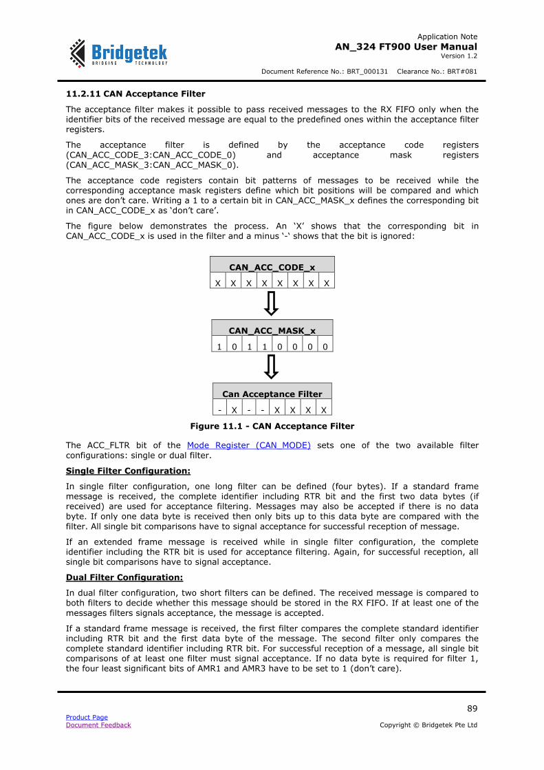
Application Note
AN_324 FT900 User Manual Version 1.2
Document Reference No.: BRT_000131 Clearance No.: BRT#081
89 Product Page Document Feedback Copyright © Bridgetek Pte Ltd
11.2.11 CAN Acceptance Filter
The acceptance filter makes it possible to pass received messages to the RX FIFO only when the identifier bits of the received message are equal to the predefined ones within the acceptance filter registers.
The acceptance filter is defined by the acceptance code registers
(CAN_ACC_CODE_3:CAN_ACC_CODE_0) and acceptance mask registers (CAN_ACC_MASK_3:CAN_ACC_MASK_0).
The acceptance code registers contain bit patterns of messages to be received while the corresponding acceptance mask registers define which bit positions will be compared and which ones are don’t care. Writing a 1 to a certain bit in CAN_ACC_MASK_x defines the corresponding bit in CAN_ACC_CODE_x as ‘don’t care’.
The figure below demonstrates the process. An ‘X’ shows that the corresponding bit in CAN_ACC_CODE_x is used in the filter and a minus ‘-‘ shows that the bit is ignored:
CAN_ACC_CODE_x
X X X X X X X X
CAN_ACC_MASK_x
1 0 1 1 0 0 0 0
Can Acceptance Filter
- X - - X X X X
Figure 11.1 - CAN Acceptance Filter
The ACC_FLTR bit of the Mode Register (CAN_MODE) sets one of the two available filter
configurations: single or dual filter.
Single Filter Configuration:
In single filter configuration, one long filter can be defined (four bytes). If a standard frame message is received, the complete identifier including RTR bit and the first two data bytes (if received) are used for acceptance filtering. Messages may also be accepted if there is no data byte. If only one data byte is received then only bits up to this data byte are compared with the
filter. All single bit comparisons have to signal acceptance for successful reception of message.
If an extended frame message is received while in single filter configuration, the complete identifier including the RTR bit is used for acceptance filtering. Again, for successful reception, all single bit comparisons have to signal acceptance.
Dual Filter Configuration:
In dual filter configuration, two short filters can be defined. The received message is compared to
both filters to decide whether this message should be stored in the RX FIFO. If at least one of the
messages filters signals acceptance, the message is accepted.
If a standard frame message is received, the first filter compares the complete standard identifier including RTR bit and the first data byte of the message. The second filter only compares the complete standard identifier including RTR bit. For successful reception of a message, all single bit comparisons of at least one filter must signal acceptance. If no data byte is required for filter 1, the four least significant bits of AMR1 and AMR3 have to be set to 1 (don’t care).
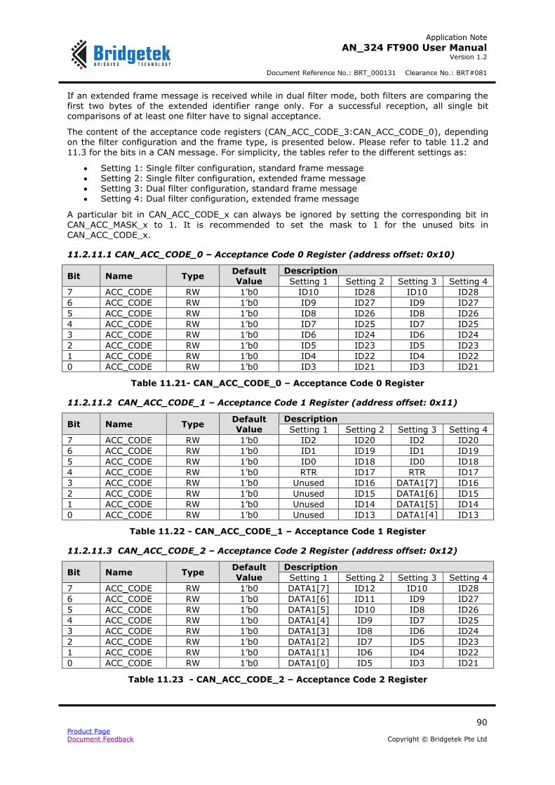
Application Note
AN_324 FT900 User Manual Version 1.2
Document Reference No.: BRT_000131 Clearance No.: BRT#081
90 Product Page Document Feedback Copyright © Bridgetek Pte Ltd
If an extended frame message is received while in dual filter mode, both filters are comparing the first two bytes of the extended identifier range only. For a successful reception, all single bit comparisons of at least one filter have to signal acceptance.
The content of the acceptance code registers (CAN_ACC_CODE_3:CAN_ACC_CODE_0), depending on the filter configuration and the frame type, is presented below. Please refer to table 11.2 and
11.3 for the bits in a CAN message. For simplicity, the tables refer to the different settings as:
Setting 1: Single filter configuration, standard frame message Setting 2: Single filter configuration, extended frame message Setting 3: Dual filter configuration, standard frame message Setting 4: Dual filter configuration, extended frame message
A particular bit in CAN_ACC_CODE_x can always be ignored by setting the corresponding bit in
CAN_ACC_MASK_x to 1. It is recommended to set the mask to 1 for the unused bits in CAN_ACC_CODE_x.
11.2.11.1 CAN_ACC_CODE_0 – Acceptance Code 0 Register (address offset: 0x10)
Bit Name Type Default Value
Description
Setting 1 Setting 2 Setting 3 Setting 4
7 ACC_CODE RW 1’b0 ID10 ID28 ID10 ID28
6 ACC_CODE RW 1’b0 ID9 ID27 ID9 ID27
5 ACC_CODE RW 1’b0 ID8 ID26 ID8 ID26
4 ACC_CODE RW 1’b0 ID7 ID25 ID7 ID25
3 ACC_CODE RW 1’b0 ID6 ID24 ID6 ID24
2 ACC_CODE RW 1’b0 ID5 ID23 ID5 ID23
1 ACC_CODE RW 1’b0 ID4 ID22 ID4 ID22
0 ACC_CODE RW 1’b0 ID3 ID21 ID3 ID21
Table 11.21- CAN_ACC_CODE_0 – Acceptance Code 0 Register
11.2.11.2 CAN_ACC_CODE_1 – Acceptance Code 1 Register (address offset: 0x11)
Bit Name Type Default Value
Description
Setting 1 Setting 2 Setting 3 Setting 4
7 ACC_CODE RW 1’b0 ID2 ID20 ID2 ID20
6 ACC_CODE RW 1’b0 ID1 ID19 ID1 ID19
5 ACC_CODE RW 1’b0 ID0 ID18 ID0 ID18
4 ACC_CODE RW 1’b0 RTR ID17 RTR ID17
3 ACC_CODE RW 1’b0 Unused ID16 DATA1[7] ID16
2 ACC_CODE RW 1’b0 Unused ID15 DATA1[6] ID15
1 ACC_CODE RW 1’b0 Unused ID14 DATA1[5] ID14
0 ACC_CODE RW 1’b0 Unused ID13 DATA1[4] ID13
Table 11.22 - CAN_ACC_CODE_1 – Acceptance Code 1 Register
11.2.11.3 CAN_ACC_CODE_2 – Acceptance Code 2 Register (address offset: 0x12)
Bit Name Type Default
Value
Description
Setting 1 Setting 2 Setting 3 Setting 4
7 ACC_CODE RW 1’b0 DATA1[7] ID12 ID10 ID28
6 ACC_CODE RW 1’b0 DATA1[6] ID11 ID9 ID27
5 ACC_CODE RW 1’b0 DATA1[5] ID10 ID8 ID26
4 ACC_CODE RW 1’b0 DATA1[4] ID9 ID7 ID25
3 ACC_CODE RW 1’b0 DATA1[3] ID8 ID6 ID24
2 ACC_CODE RW 1’b0 DATA1[2] ID7 ID5 ID23
1 ACC_CODE RW 1’b0 DATA1[1] ID6 ID4 ID22
0 ACC_CODE RW 1’b0 DATA1[0] ID5 ID3 ID21
Table 11.23 - CAN_ACC_CODE_2 – Acceptance Code 2 Register
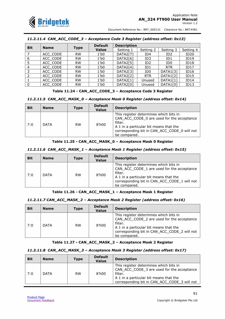
Application Note
AN_324 FT900 User Manual Version 1.2
Document Reference No.: BRT_000131 Clearance No.: BRT#081
91 Product Page Document Feedback Copyright © Bridgetek Pte Ltd
11.2.11.4 CAN_ACC_CODE_3 – Acceptance Code 3 Register (address offset: 0x13)
Bit Name Type Default Value
Description
Setting 1 Setting 2 Setting 3 Setting 4
7 ACC_CODE RW 1’b0 DATA2[7] ID4 ID2 ID20
6 ACC_CODE RW 1’b0 DATA2[6] ID3 ID1 ID19
5 ACC_CODE RW 1’b0 DATA2[5] ID2 ID0 ID18
4 ACC_CODE RW 1’b0 DATA2[4] ID1 RTR ID17
3 ACC_CODE RW 1’b0 DATA2[3] ID0 DATA1[3] ID16
2 ACC_CODE RW 1’b0 DATA2[2] RTR DATA1[2] ID15
1 ACC_CODE RW 1’b0 DATA2[1] Unused DATA1[1] ID14
0 ACC_CODE RW 1’b0 DATA2[0] Unused DATA1[0] ID13
Table 11.24 - CAN_ACC_CODE_3 – Acceptance Code 3 Register
11.2.11.5 CAN_ACC_MASK_0 – Acceptance Mask 0 Register (address offset: 0x14)
Bit Name Type Default Value
Description
7:0 DATA RW 8’h00
This register determines which bits in CAN_ACC_CODE_0 are used for the acceptance filter. A 1 in a particular bit means that the corresponding bit in CAN_ACC_CODE_0 will not be compared.
Table 11.25 - CAN_ACC_MASK_0 – Acceptance Mask 0 Register
11.2.11.6 CAN_ACC_MASK_1 – Acceptance Mask 1 Register (address offset: 0x15)
Bit Name Type Default
Value Description
7:0 DATA RW 8’h00
This register determines which bits in CAN_ACC_CODE_1 are used for the acceptance filter. A 1 in a particular bit means that the
corresponding bit in CAN_ACC_CODE_1 will not be compared.
Table 11.26 - CAN_ACC_MASK_1 – Acceptance Mask 1 Register
11.2.11.7 CAN_ACC_MASK_2 – Acceptance Mask 2 Register (address offset: 0x16)
Bit Name Type Default Value
Description
7:0 DATA RW 8’h00
This register determines which bits in CAN_ACC_CODE_2 are used for the acceptance
filter. A 1 in a particular bit means that the corresponding bit in CAN_ACC_CODE_2 will not be compared.
Table 11.27 - CAN_ACC_MASK_2 – Acceptance Mask 2 Register
11.2.11.8 CAN_ACC_MASK_3 – Acceptance Mask 3 Register (address offset: 0x17)
Bit Name Type Default Value
Description
7:0 DATA RW 8’h00
This register determines which bits in CAN_ACC_CODE_3 are used for the acceptance filter. A 1 in a particular bit means that the corresponding bit in CAN_ACC_CODE_3 will not
Application Note
AN_324 FT900 User Manual Version 1.2
Document Reference No.: BRT_000131 Clearance No.: BRT#081
92 Product Page Document Feedback Copyright © Bridgetek Pte Ltd
Bit Name Type Default Value
Description
be compared.
Table 11.28 - CAN_ACC_MASK_3 – Acceptance Mask 3 Register
11.2.12 CAN_ERR_CODE – Error Code Capture Register (address offset: 0x18)
Bit Name Type Default Value
Description
7 RX_WRN RO 1’b0 Set when RX_ERR counter is greater than or equal to 96.
6 TX_WRN RO 1’b0 Set when TX_ERR counter is greater than or equal to 96.
5 ERR_DIR RO 1’b0
Direction of transfer when error occurred.
0: transmission 1: reception
4 ACK_ERR RO 1’b0 ACK error occurred.
3 FRM_ERR RO 1’b0 Form error occurred.
2 CRC_ERR RO 1’b0 CRC error occurred.
1 STF_ERR RO 1’b0 Stuff error occurred.
0 BIT_ERR RO 1’b0 Bit error occurred.
Table 11.29 - CAN_ERR_CODE – Error Code Capture Register
11.2.13 CAN_RX_ERR_CNTR – Receive Error Counter Register (address offset: 0x19)
Bit Name Type Default
Value Description
7:0 RX_ERR RO 8’h00 This is the current receive error counter. If a bus off event occurs, it is initialized to 0.
Table 11.30 - CAN_RX_ERR_CNTR – Receive Error Counter Register
11.2.14 CAN_TX_ERR_CNTR – Transmit Error Counter Register (address offset: 0x1A)
Bit Name Type Default Value
Description
7:0 TX_ERR RO 8’h00
This is the low-byte of the current transmit error counter as the width of the transmit error counter is 9-bit.
If a bus off event occurs, it is initialized to 127 to count the minimum protocol defined time (128 occurrences of bus free signal). Reading TX_ERR during this time gives information about the status of the bus off recovery.
Table 11.31 - CAN_TX_ERR_CNTR – Transmit Error Counter Register
11.2.15 CAN_ARB_LOST_CODE – Arbitration Lost Code Capture Register (address offset:
0x1B)
Bit Name Type Default Value
Description
7:5 Reserved - - -
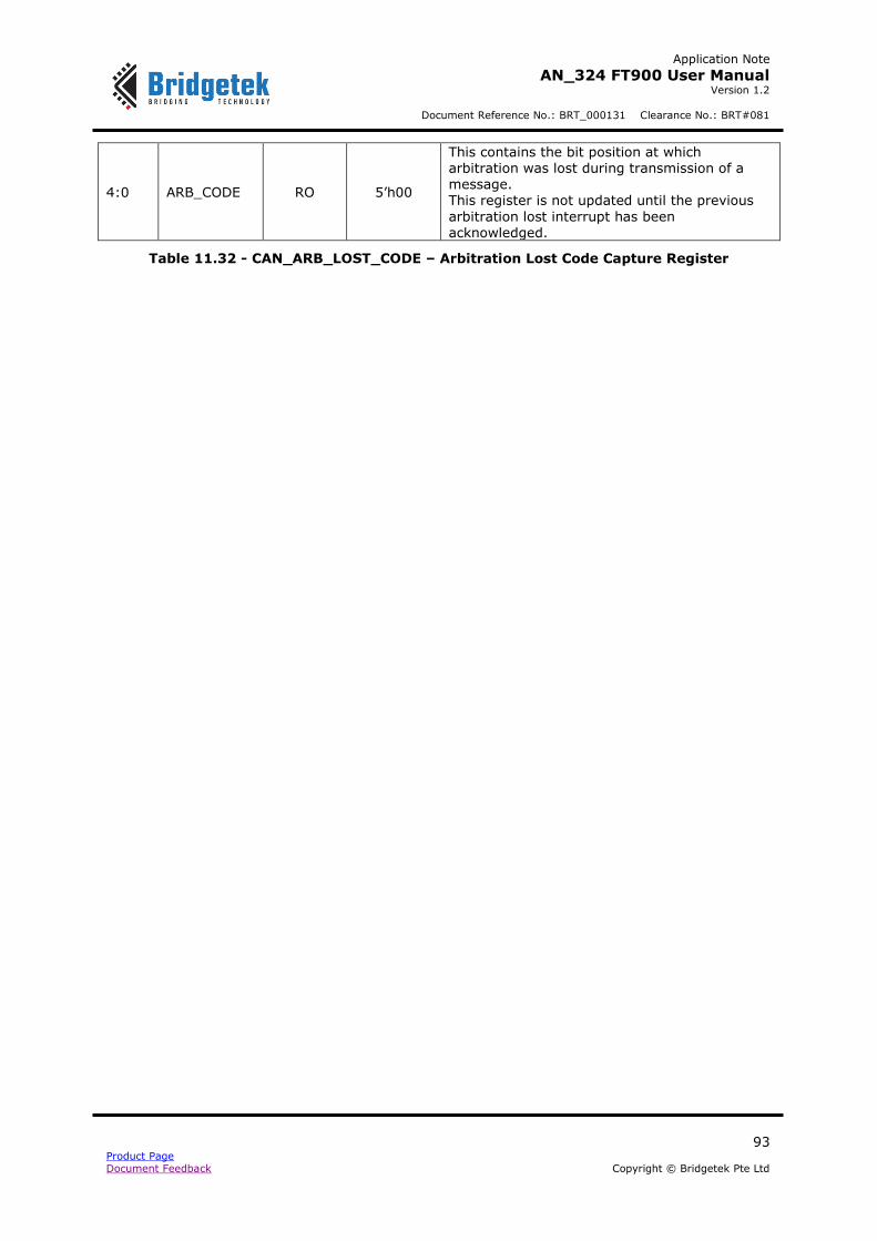
Application Note
AN_324 FT900 User Manual Version 1.2
Document Reference No.: BRT_000131 Clearance No.: BRT#081
93 Product Page Document Feedback Copyright © Bridgetek Pte Ltd
4:0 ARB_CODE RO 5’h00
This contains the bit position at which arbitration was lost during transmission of a message. This register is not updated until the previous
arbitration lost interrupt has been acknowledged.
Table 11.32 - CAN_ARB_LOST_CODE – Arbitration Lost Code Capture Register

Application Note
AN_324 FT900 User Manual Version 1.2
Document Reference No.: BRT_000131 Clearance No.: BRT#081
94 Product Page Document Feedback Copyright © Bridgetek Pte Ltd
12 SD Host
The device supports a SD Host with the following features.
Supports PIO data transfers
Supports configurable SD bus modes: 4-bit mode and 8-bit mode
Supports configurable 8-word/16-word register for data FIFO
Supports configurable 1K/2K/4K SRAM for data FIFO
Supports configurable 1-bit/4-bit SD card bus and 1-bit/4-bit/8-bit MMC card bus
Configurable CPRM function for security
Built-in generation and check for 7-bit and 16-bit CRC data
Card detection (Insertion/Removal)
Supports Read Wait mechanism for SDIO function
Supports Suspend/Resume mechanism for SDIO function
12.1 Register Summary
Listed below are the registers with their offset from the base address (0x10400). All registers can only be accessed via Double-Word (32-bit) mode. Note that some registers are not 32-bit long. In that case, several registers are combined into one 32-bit location. If one such register is accessed, all other registers in the same 32-bit location will also be affected. The users need to take care not
to modify the content of the other registers.
Address Offset
Register Default value
References
0x00 SDH_AUTO_CMD23_ARG2 – Auto CMD23 Argument 2 Register
0x00000000 Section 12.2.1
0x04 SDH_BLK_SIZE – Block Size Register 0x0000 Section 12.2.2
0x06 SDH_BLK_COUNT – Block Count Register 0x0000 Section 12.2.3
0x08 SDH_ARG_1 – Argument 1 Register 0x00000000 Section 12.2.4
0x0C SDH_TNSFER_MODE – Transfer Mode Register 0x0000 Section 12.2.5
0x0E SDH_CMD – Command Register 0x0000 Section 12.2.6
0x10 -
0x1C
SDH_RESPONSE – Response Register 0x00000000 Section 12.2.7
0x20 SDH_BUF_DATA – Buffer Data Port Register 0x00000000 Section 12.2.8
0x24 SDH_PRESENT_STATE – Present State Register 0x00000000 Section 12.2.9
0x28 SDH_HST_CNTL_1 – Host Control 1 Register 0x00 Section 12.2.10
0x29 SDH_PWR_CNTL – Power Control Register 0x00 Section 12.2.11

Application Note
AN_324 FT900 User Manual Version 1.2
Document Reference No.: BRT_000131 Clearance No.: BRT#081
95 Product Page Document Feedback Copyright © Bridgetek Pte Ltd
0x2A SDH_BLK_GAP_CNTL – Block Gap Control Register 0x0000 Section 12.2.12
0x2C SDH_CLK_GAP_CNTL – Clock Control Register 0x0000 Section 12.2.13
0x2E SDH_TIMEOUT_CNTL – Timeout Control Register 0x00 Section 12.2.14
0x2F SDH_SW_RST – Software Reset Register 0x00 Section 12.2.15
0x30 SDH_NRML_INT_STATUS – Normal Interrupt
Status Register
0x0000 Section 12.2.16
0x32 SDH_ERR_INT_STATUS – Error Interrupt Status
Register 0x0000 Section 12.2.17
0x34 SDH_NRML_INT_ENABLE – Normal Interrupt
Status Enable Register 0x0000 Section 12.2.18
0x36 SDH_ERR_INT_ENABLE – Error Interrupt Status
Enable Register 0x0000 Section 12.2.19
0x38 SDH_NRML_INT_SGNL_ENABLE – Normal Interrupt Signal Enable Register
0x0000 Section 12.2.20
0x3A SDH_ERR_INT_SGNL_ENABLE – Error Interrupt Signal Enable Register
0x0000 Section 12.2.21
0x3C SDH_AUTO_CMD12_ERR_STATUS – Auto CMD12 Error Status Register
0x0000 Section 12.2.22
0x3E SDH_HOST_CNTL_2 – Host Control 2 Register 0x0000 Section 12.2.23
0x40 SDH_CAP_1 – Capabilities Register 1 0x016A0080 Section 12.2.24
0x44 SDH_CAP_2 – Capabilities Register 2 0x00000F75 Section 12.2.25
0x48 SDH_RSRV_1 – Reserved 1 Register 0x00000000 Section 12.2.26
0x4C SDH_RSRV_2 – Reserved 2 Register 0x00000000 Section 12.2.27
0x50 SDH_FORCE_EVT_CMD_ERR_STATUS – Force
Event for Auto CMD Error Status Register 0x0000 Section 12.2.28
0x52 SDH_FORCE_EVT_ERR_INT_STATUS – Force Event for Error Interrupt Status Register
0x0000 Section 12.2.29
0x54 SDH_RSRV_3 – Reserved 3 Register 0x00000000 Section 12.2.30
0x58 SDH_RSRV_4 – Reserved 4 Register 0x00000000 Section 12.2.31
0x60 SDH_PRST_INIT – Preset value for initialization Register
0x0000 Section 12.2.32
0x62 SDH_PRST_DFLT_SPD – Preset value for default speed Register
0x0000 Section 12.2.33
0x64 SDH_PRST_HIGH_SPD – Preset value for the high speed Register
0x0000 Section 12.2.34
0x66 SDH_PRST_SDR12 – Preset value for SDR12 Register
0x0000 Section 12.2.35
0x68 SDH_PRST_SDR25 – Preset value for SDR25
Register
0x0000 Section 12.2.36
0x6A SDH_PRST_SDR50 – Preset value for SDR50
Register
0x0000 Section 12.2.37
0x6C SDH_PRST_SDR104 – Preset value for SDR104
Register 0x0000 Section 12.2.38
0x6E SDH_PRST_DDR50 – Preset value for DDR50
Register 0x0000 Section 12.2.39
0xFC SDH_RSRV_5 – Reserved 5 Register 0x0000 Section 12.2.40
0xFE SDH_HC_VER – Host Controller Version Register 0x0002 Section 12.2.41
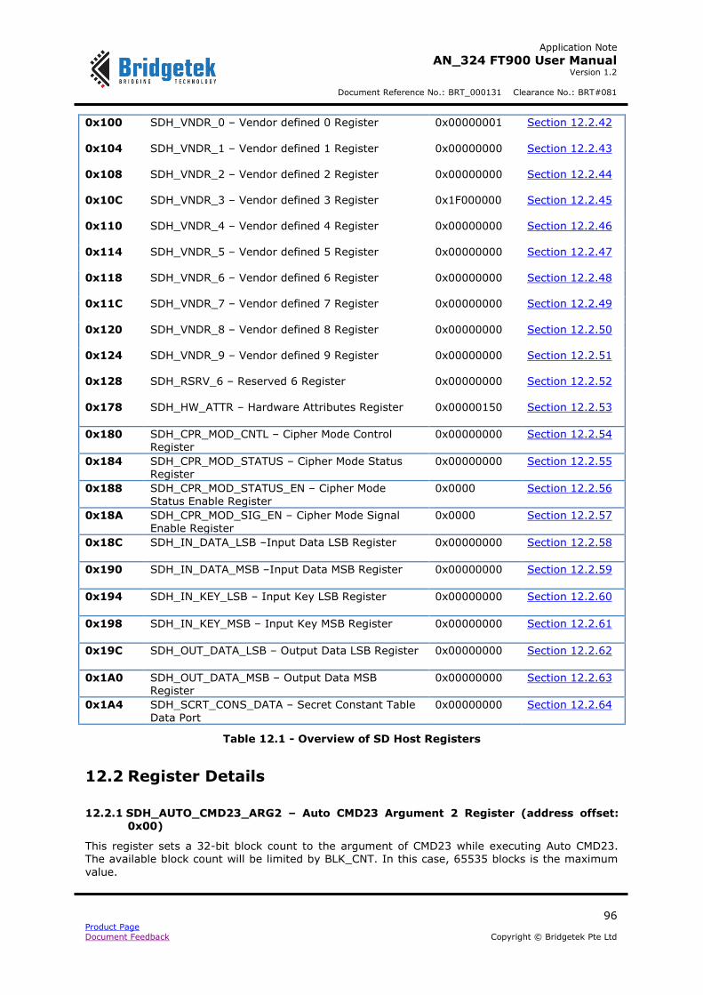
Application Note
AN_324 FT900 User Manual Version 1.2
Document Reference No.: BRT_000131 Clearance No.: BRT#081
96 Product Page Document Feedback Copyright © Bridgetek Pte Ltd
0x100 SDH_VNDR_0 – Vendor defined 0 Register 0x00000001 Section 12.2.42
0x104 SDH_VNDR_1 – Vendor defined 1 Register 0x00000000 Section 12.2.43
0x108 SDH_VNDR_2 – Vendor defined 2 Register 0x00000000 Section 12.2.44
0x10C SDH_VNDR_3 – Vendor defined 3 Register 0x1F000000 Section 12.2.45
0x110 SDH_VNDR_4 – Vendor defined 4 Register 0x00000000 Section 12.2.46
0x114 SDH_VNDR_5 – Vendor defined 5 Register 0x00000000 Section 12.2.47
0x118 SDH_VNDR_6 – Vendor defined 6 Register 0x00000000 Section 12.2.48
0x11C SDH_VNDR_7 – Vendor defined 7 Register 0x00000000 Section 12.2.49
0x120 SDH_VNDR_8 – Vendor defined 8 Register 0x00000000 Section 12.2.50
0x124 SDH_VNDR_9 – Vendor defined 9 Register 0x00000000 Section 12.2.51
0x128 SDH_RSRV_6 – Reserved 6 Register 0x00000000 Section 12.2.52
0x178 SDH_HW_ATTR – Hardware Attributes Register 0x00000150 Section 12.2.53
0x180 SDH_CPR_MOD_CNTL – Cipher Mode Control Register
0x00000000 Section 12.2.54
0x184 SDH_CPR_MOD_STATUS – Cipher Mode Status Register
0x00000000 Section 12.2.55
0x188 SDH_CPR_MOD_STATUS_EN – Cipher Mode
Status Enable Register
0x0000 Section 12.2.56
0x18A SDH_CPR_MOD_SIG_EN – Cipher Mode Signal Enable Register
0x0000 Section 12.2.57
0x18C SDH_IN_DATA_LSB –Input Data LSB Register 0x00000000 Section 12.2.58
0x190 SDH_IN_DATA_MSB –Input Data MSB Register 0x00000000 Section 12.2.59
0x194 SDH_IN_KEY_LSB – Input Key LSB Register 0x00000000 Section 12.2.60
0x198 SDH_IN_KEY_MSB – Input Key MSB Register 0x00000000 Section 12.2.61
0x19C SDH_OUT_DATA_LSB – Output Data LSB Register 0x00000000 Section 12.2.62
0x1A0 SDH_OUT_DATA_MSB – Output Data MSB Register
0x00000000 Section 12.2.63
0x1A4 SDH_SCRT_CONS_DATA – Secret Constant Table
Data Port
0x00000000 Section 12.2.64
Table 12.1 - Overview of SD Host Registers
12.2 Register Details
12.2.1 SDH_AUTO_CMD23_ARG2 – Auto CMD23 Argument 2 Register (address offset: 0x00)
This register sets a 32-bit block count to the argument of CMD23 while executing Auto CMD23. The available block count will be limited by BLK_CNT. In this case, 65535 blocks is the maximum
value.
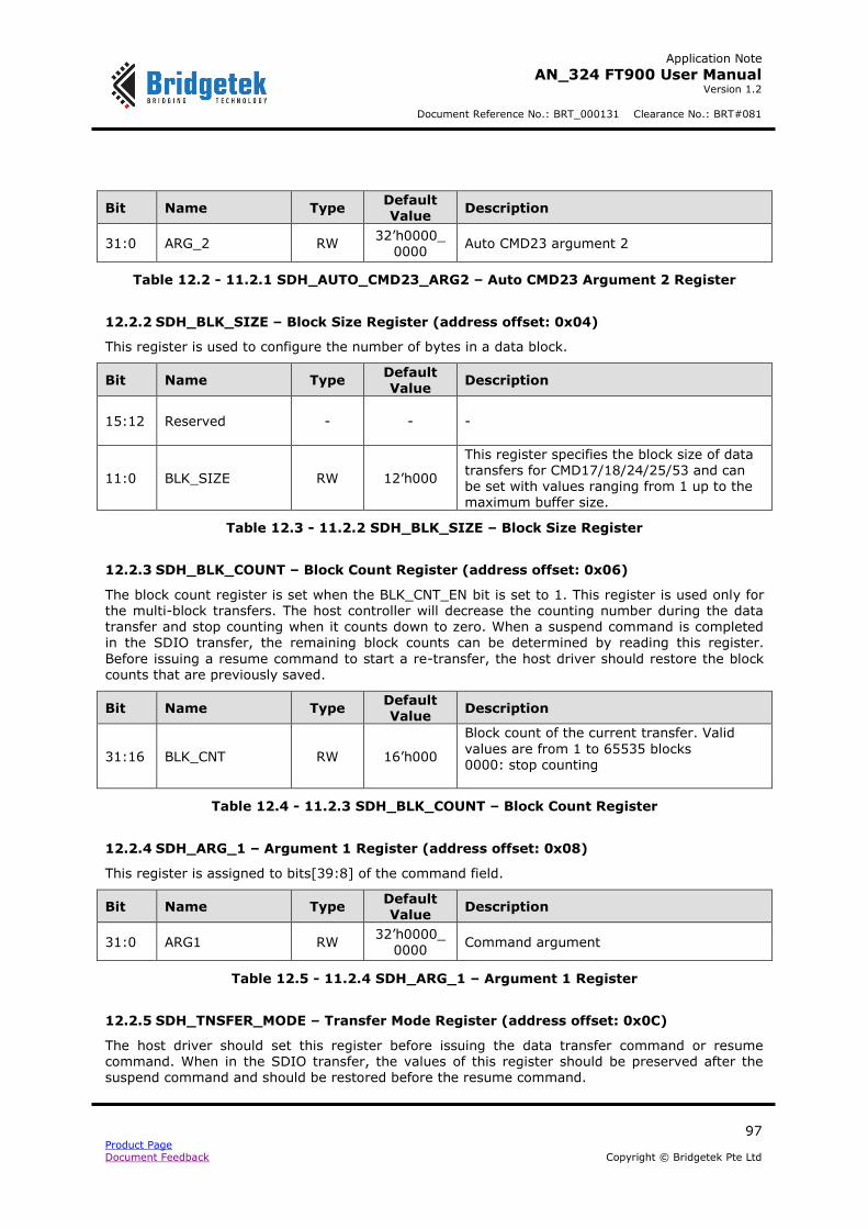
Application Note
AN_324 FT900 User Manual Version 1.2
Document Reference No.: BRT_000131 Clearance No.: BRT#081
97 Product Page Document Feedback Copyright © Bridgetek Pte Ltd
Bit Name Type Default Value
Description
31:0 ARG_2 RW 32’h0000_
0000 Auto CMD23 argument 2
Table 12.2 - 11.2.1 SDH_AUTO_CMD23_ARG2 – Auto CMD23 Argument 2 Register
12.2.2 SDH_BLK_SIZE – Block Size Register (address offset: 0x04)
This register is used to configure the number of bytes in a data block.
Bit Name Type Default Value
Description
15:12 Reserved - - -
11:0 BLK_SIZE RW 12’h000
This register specifies the block size of data transfers for CMD17/18/24/25/53 and can be set with values ranging from 1 up to the maximum buffer size.
Table 12.3 - 11.2.2 SDH_BLK_SIZE – Block Size Register
12.2.3 SDH_BLK_COUNT – Block Count Register (address offset: 0x06)
The block count register is set when the BLK_CNT_EN bit is set to 1. This register is used only for the multi-block transfers. The host controller will decrease the counting number during the data transfer and stop counting when it counts down to zero. When a suspend command is completed in the SDIO transfer, the remaining block counts can be determined by reading this register.
Before issuing a resume command to start a re-transfer, the host driver should restore the block counts that are previously saved.
Bit Name Type Default Value
Description
31:16 BLK_CNT RW 16’h000
Block count of the current transfer. Valid
values are from 1 to 65535 blocks 0000: stop counting
Table 12.4 - 11.2.3 SDH_BLK_COUNT – Block Count Register
12.2.4 SDH_ARG_1 – Argument 1 Register (address offset: 0x08)
This register is assigned to bits[39:8] of the command field.
Bit Name Type Default Value
Description
31:0 ARG1 RW 32’h0000_
0000 Command argument
Table 12.5 - 11.2.4 SDH_ARG_1 – Argument 1 Register
12.2.5 SDH_TNSFER_MODE – Transfer Mode Register (address offset: 0x0C)
The host driver should set this register before issuing the data transfer command or resume command. When in the SDIO transfer, the values of this register should be preserved after the suspend command and should be restored before the resume command.
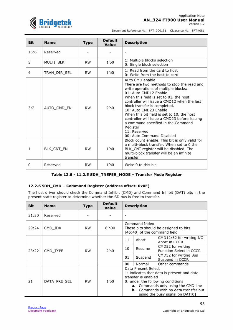
Application Note
AN_324 FT900 User Manual Version 1.2
Document Reference No.: BRT_000131 Clearance No.: BRT#081
98 Product Page Document Feedback Copyright © Bridgetek Pte Ltd
Bit Name Type Default Value
Description
15:6 Reserved - - -
5 MULTI_BLK RW 1’b0 1: Multiple blocks selection 0: Single block selection
4 TRAN_DIR_SEL RW 1’b0 1: Read from the card to host 0: Write from the host to card
3:2 AUTO_CMD_EN RW 2’h0
Auto CMD enable There are two methods to stop the read and write operations of multiple blocks: 01: Auto CMD12 Enable When this field is set to 01, the host controller will issue a CMD12 when the last block transfer is completed.
10: Auto CMD23 Enable When this bit field is set to 10, the host controller will issue a CMD23 before issuing a command specified in the Command Register 11: Reserved 00: Auto Command Disabled
1 BLK_CNT_EN RW 1’b0
Block count enable. This bit is only valid for a multi-block transfer. When set to 0 the BLK_CNT register will be disabled. The multi-block transfer will be an infinite transfer
0 Reserved RW 1’b0 Write 0 to this bit
Table 12.6 - 11.2.5 SDH_TNSFER_MODE – Transfer Mode Register
12.2.6 SDH_CMD – Command Register (address offset: 0x0E)
The host driver should check the Command Inhibit (CMD) and Command Inhibit (DAT) bits in the present state register to determine whether the SD bus is free to transfer.
Bit Name Type Default Value
Description
31:30 Reserved - - -
29:24 CMD_IDX RW 6’h00 Command Index These bits should be assigned to bits [45:40] of the command field
23:22 CMD_TYPE RW 2’h0
11 Abort CMD12/52 for writing I/O Abort in CCCR
10 Resume CMD52 for writing Function Select in CCCR
01 Suspend CMD52 for writing Bus
Suspend in CCCR
00 Normal Other commands
21 DATA_PRE_SEL RW 1’b0
Data Present Select 1: indicates that data is present and data transfer is enabled 0: under the following conditions
a. Commands only using the CMD line
b. Commands with no data transfer but using the busy signal on DAT[0]
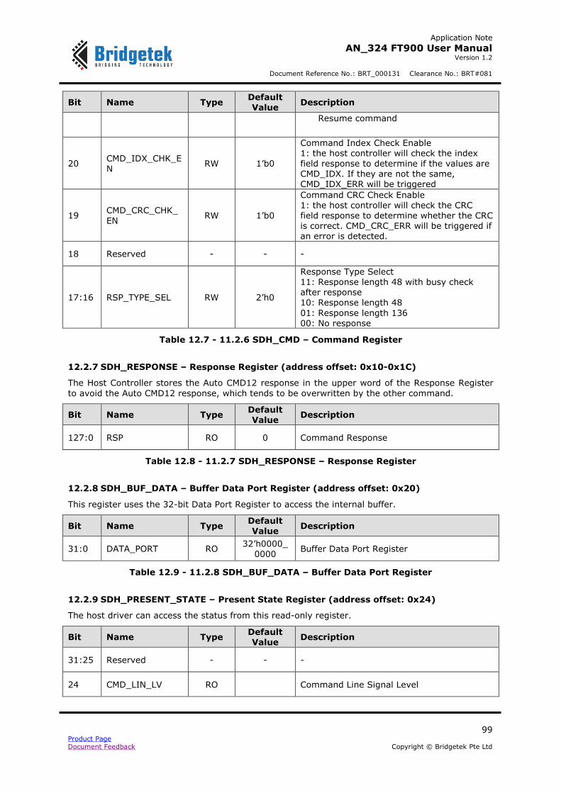
Application Note
AN_324 FT900 User Manual Version 1.2
Document Reference No.: BRT_000131 Clearance No.: BRT#081
99 Product Page Document Feedback Copyright © Bridgetek Pte Ltd
Bit Name Type Default Value
Description
Resume command
20 CMD_IDX_CHK_EN
RW 1’b0
Command Index Check Enable 1: the host controller will check the index field response to determine if the values are CMD_IDX. If they are not the same, CMD_IDX_ERR will be triggered
19 CMD_CRC_CHK_
EN RW 1’b0
Command CRC Check Enable 1: the host controller will check the CRC field response to determine whether the CRC is correct. CMD_CRC_ERR will be triggered if an error is detected.
18 Reserved - - -
17:16 RSP_TYPE_SEL RW 2’h0
Response Type Select 11: Response length 48 with busy check after response 10: Response length 48
01: Response length 136 00: No response
Table 12.7 - 11.2.6 SDH_CMD – Command Register
12.2.7 SDH_RESPONSE – Response Register (address offset: 0x10-0x1C)
The Host Controller stores the Auto CMD12 response in the upper word of the Response Register
to avoid the Auto CMD12 response, which tends to be overwritten by the other command.
Bit Name Type Default Value
Description
127:0 RSP RO 0 Command Response
Table 12.8 - 11.2.7 SDH_RESPONSE – Response Register
12.2.8 SDH_BUF_DATA – Buffer Data Port Register (address offset: 0x20)
This register uses the 32-bit Data Port Register to access the internal buffer.
Bit Name Type Default Value
Description
31:0 DATA_PORT RO 32’h0000_
0000 Buffer Data Port Register
Table 12.9 - 11.2.8 SDH_BUF_DATA – Buffer Data Port Register
12.2.9 SDH_PRESENT_STATE – Present State Register (address offset: 0x24)
The host driver can access the status from this read-only register.
Bit Name Type Default Value
Description
31:25 Reserved - - -
24 CMD_LIN_LV RO Command Line Signal Level
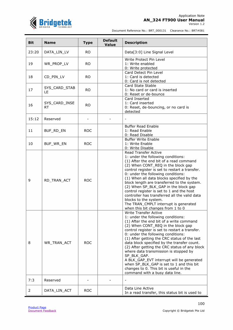
Application Note
AN_324 FT900 User Manual Version 1.2
Document Reference No.: BRT_000131 Clearance No.: BRT#081
100 Product Page Document Feedback Copyright © Bridgetek Pte Ltd
Bit Name Type Default Value
Description
23:20 DATA_LIN_LV RO Data[3:0] Line Signal Level
19 WR_PROP_LV RO Write Protect Pin Level 1: Write enabled 0: Write protected
18 CD_PIN_LV RO
Card Detect Pin Level
1: Card is detected 0: Card is not detected
17 SYS_CARD_STABLE
RO Card State Stable 1: No card or card is inserted 0: Reset or de-bounce
16 SYS_CARD_INSERT
RO
Card Inserted 1: Card inserted 0: Reset, de-bouncing, or no card is
detected
15:12 Reserved - - -
11 BUF_RD_EN ROC Buffer Read Enable 1: Read Enable 0: Read Disable
10 BUF_WR_EN ROC
Buffer Write Enable
1: Write Enable 0: Write Disable
9 RD_TRAN_ACT ROC
Read Transfer Active 1: under the following conditions: (1) After the end bit of a read command (2) When CONT_REQ in the block gap
control register is set to restart a transfer. 0: under the following conditions: (1) When all data blocks specified by the block length are transferred to the system.
(2) When SP_BLK_GAP in the block gap control register is set to 1 and the host
controller has transferred all the valid data blocks to the system. The TRAN_CMPLT interrupt is generated when this bit changes from 1 to 0
8 WR_TRAN_ACT ROC
Write Transfer Active 1: under the following conditions:
(1) After the end bit of a write command (2) When CONT_REQ in the block gap control register is set to restart a transfer. 0: under the following conditions: (1) After getting the CRC status of the last data block specified by the transfer count. (2) After getting the CRC status of any block
where data transmission is stopped by SP_BLK_GAP.
A BLK_GAP_EVT interrupt will be generated when SP_BLK_GAP is set to 1 and this bit changes to 0. This bit is useful in the command with a busy data line.
7:3 Reserved - - -
2 DATA_LIN_ACT ROC Data Line Active In a read transfer, this status bit is used to
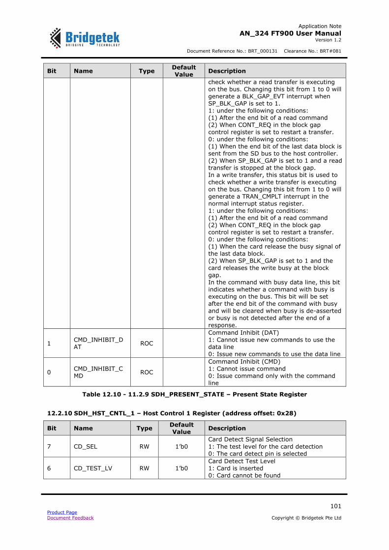
Application Note
AN_324 FT900 User Manual Version 1.2
Document Reference No.: BRT_000131 Clearance No.: BRT#081
101 Product Page Document Feedback Copyright © Bridgetek Pte Ltd
Bit Name Type Default Value
Description
check whether a read transfer is executing on the bus. Changing this bit from 1 to 0 will generate a BLK_GAP_EVT interrupt when SP_BLK_GAP is set to 1. 1: under the following conditions: (1) After the end bit of a read command (2) When CONT_REQ in the block gap
control register is set to restart a transfer. 0: under the following conditions: (1) When the end bit of the last data block is sent from the SD bus to the host controller. (2) When SP_BLK_GAP is set to 1 and a read transfer is stopped at the block gap. In a write transfer, this status bit is used to
check whether a write transfer is executing on the bus. Changing this bit from 1 to 0 will generate a TRAN_CMPLT interrupt in the normal interrupt status register. 1: under the following conditions: (1) After the end bit of a read command
(2) When CONT_REQ in the block gap control register is set to restart a transfer. 0: under the following conditions: (1) When the card release the busy signal of the last data block. (2) When SP_BLK_GAP is set to 1 and the card releases the write busy at the block
gap. In the command with busy data line, this bit indicates whether a command with busy is executing on the bus. This bit will be set after the end bit of the command with busy
and will be cleared when busy is de-asserted or busy is not detected after the end of a
response.
1 CMD_INHIBIT_DAT
ROC
Command Inhibit (DAT) 1: Cannot issue new commands to use the data line 0: Issue new commands to use the data line
0 CMD_INHIBIT_CMD
ROC
Command Inhibit (CMD) 1: Cannot issue command 0: Issue command only with the command line
Table 12.10 - 11.2.9 SDH_PRESENT_STATE – Present State Register
12.2.10 SDH_HST_CNTL_1 – Host Control 1 Register (address offset: 0x28)
Bit Name Type Default
Value Description
7 CD_SEL RW 1’b0
Card Detect Signal Selection
1: The test level for the card detection 0: The card detect pin is selected
6 CD_TEST_LV RW 1’b0 Card Detect Test Level 1: Card is inserted 0: Card cannot be found
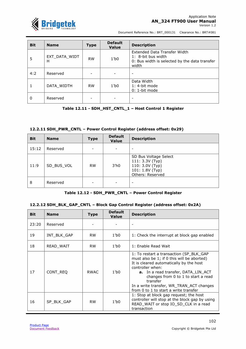
Application Note
AN_324 FT900 User Manual Version 1.2
Document Reference No.: BRT_000131 Clearance No.: BRT#081
102 Product Page Document Feedback Copyright © Bridgetek Pte Ltd
Bit Name Type Default Value
Description
5 EXT_DATA_WIDTH
RW 1’b0
Extended Data Transfer Width 1: 8-bit bus width 0: Bus width is selected by the data transfer width
4:2 Reserved - - -
1 DATA_WIDTH RW 1’b0 Data Width 1: 4-bit mode 0: 1-bit mode
0 Reserved - - -
Table 12.11 - SDH_HST_CNTL_1 – Host Control 1 Register
12.2.11 SDH_PWR_CNTL – Power Control Register (address offset: 0x29)
Bit Name Type Default Value
Description
15:12 Reserved - - -
11:9 SD_BUS_VOL RW 3’h0
SD Bus Voltage Select 111: 3.3V (Typ)
110: 3.0V (Typ) 101: 1.8V (Typ) Others: Reserved
8 Reserved - - -
Table 12.12 - SDH_PWR_CNTL – Power Control Register
12.2.12 SDH_BLK_GAP_CNTL – Block Gap Control Register (address offset: 0x2A)
Bit Name Type Default Value
Description
23:20 Reserved - - -
19 INT_BLK_GAP RW 1’b0 1: Check the interrupt at block gap enabled
18 READ_WAIT RW 1’b0 1: Enable Read Wait
17 CONT_REQ RWAC 1’b0
1: To restart a transaction (SP_BLK_GAP
must also be 1; if 0 this will be aborted) It is cleared automatically by the host controller when:
a. In a read transfer, DATA_LIN_ACT changes from 0 to 1 to start a read transfer
In a write transfer, WR_TRAN_ACT changes from 0 to 1 to start a write transfer
16 SP_BLK_GAP RW 1’b0
1: Stop at block gap request; the host controller will stop at the block gap by using READ_WAIT or stop IO_SD_CLK in a read transaction
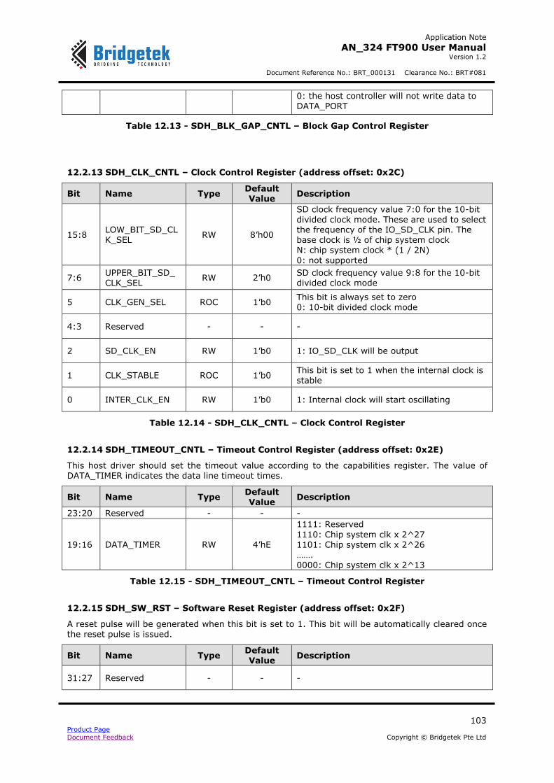
Application Note
AN_324 FT900 User Manual Version 1.2
Document Reference No.: BRT_000131 Clearance No.: BRT#081
103 Product Page Document Feedback Copyright © Bridgetek Pte Ltd
0: the host controller will not write data to DATA_PORT
Table 12.13 - SDH_BLK_GAP_CNTL – Block Gap Control Register
12.2.13 SDH_CLK_CNTL – Clock Control Register (address offset: 0x2C)
Bit Name Type Default Value
Description
15:8 LOW_BIT_SD_CLK_SEL
RW 8’h00
SD clock frequency value 7:0 for the 10-bit divided clock mode. These are used to select the frequency of the IO_SD_CLK pin. The base clock is ½ of chip system clock N: chip system clock * (1 / 2N)
0: not supported
7:6 UPPER_BIT_SD_CLK_SEL
RW 2’h0 SD clock frequency value 9:8 for the 10-bit divided clock mode
5 CLK_GEN_SEL ROC 1’b0 This bit is always set to zero 0: 10-bit divided clock mode
4:3 Reserved - - -
2 SD_CLK_EN RW 1’b0 1: IO_SD_CLK will be output
1 CLK_STABLE ROC 1’b0 This bit is set to 1 when the internal clock is stable
0 INTER_CLK_EN RW 1’b0 1: Internal clock will start oscillating
Table 12.14 - SDH_CLK_CNTL – Clock Control Register
12.2.14 SDH_TIMEOUT_CNTL – Timeout Control Register (address offset: 0x2E)
This host driver should set the timeout value according to the capabilities register. The value of DATA_TIMER indicates the data line timeout times.
Bit Name Type Default Value
Description
23:20 Reserved - - -
19:16 DATA_TIMER RW 4’hE
1111: Reserved
1110: Chip system clk x 2^27 1101: Chip system clk x 2^26 ……. 0000: Chip system clk x 2^13
Table 12.15 - SDH_TIMEOUT_CNTL – Timeout Control Register
12.2.15 SDH_SW_RST – Software Reset Register (address offset: 0x2F)
A reset pulse will be generated when this bit is set to 1. This bit will be automatically cleared once the reset pulse is issued.
Bit Name Type Default Value
Description
31:27 Reserved - - -
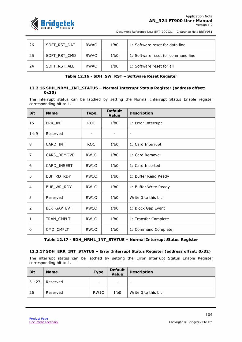
Application Note
AN_324 FT900 User Manual Version 1.2
Document Reference No.: BRT_000131 Clearance No.: BRT#081
104 Product Page Document Feedback Copyright © Bridgetek Pte Ltd
26 SOFT_RST_DAT RWAC 1’b0 1: Software reset for data line
25 SOFT_RST_CMD RWAC 1’b0 1: Software reset for command line
24 SOFT_RST_ALL RWAC 1’b0 1: Software reset for all
Table 12.16 - SDH_SW_RST – Software Reset Register
12.2.16 SDH_NRML_INT_STATUS – Normal Interrupt Status Register (address offset: 0x30)
The interrupt status can be latched by setting the Normal Interrupt Status Enable register
corresponding bit to 1.
Bit Name Type Default
Value Description
15 ERR_INT ROC 1’b0 1: Error Interrupt
14:9 Reserved - - -
8 CARD_INT ROC 1’b0 1: Card Interrupt
7 CARD_REMOVE RW1C 1’b0 1: Card Remove
6 CARD_INSERT RW1C 1’b0 1: Card Inserted
5 BUF_RD_RDY RW1C 1’b0 1: Buffer Read Ready
4 BUF_WR_RDY RW1C 1’b0 1: Buffer Write Ready
3 Reserved RW1C 1’b0 Write 0 to this bit
2 BLK_GAP_EVT RW1C 1’b0 1: Block Gap Event
1 TRAN_CMPLT RW1C 1’b0 1: Transfer Complete
0 CMD_CMPLT RW1C 1’b0 1: Command Complete
Table 12.17 - SDH_NRML_INT_STATUS – Normal Interrupt Status Register
12.2.17 SDH_ERR_INT_STATUS – Error Interrupt Status Register (address offset: 0x32)
The interrupt status can be latched by setting the Error Interrupt Status Enable Register
corresponding bit to 1.
Bit Name Type Default Value
Description
31:27 Reserved - - -
26 Reserved RW1C 1’b0 Write 0 to this bit
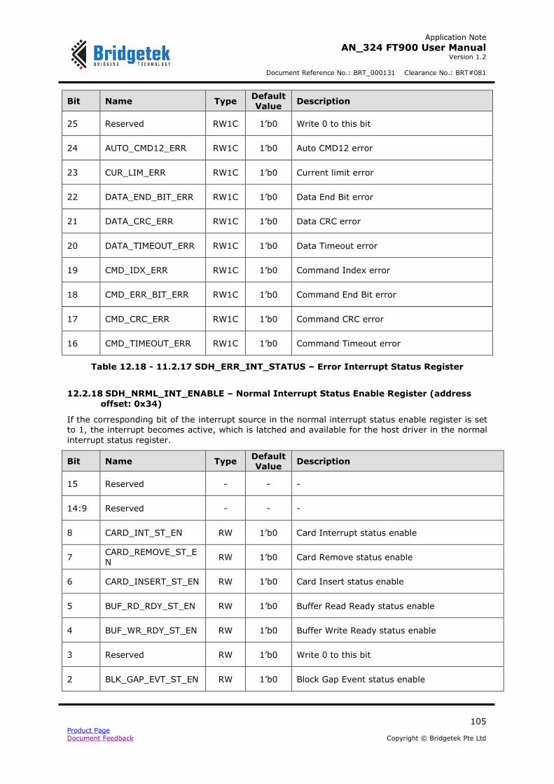
Application Note
AN_324 FT900 User Manual Version 1.2
Document Reference No.: BRT_000131 Clearance No.: BRT#081
105 Product Page Document Feedback Copyright © Bridgetek Pte Ltd
Bit Name Type Default Value
Description
25 Reserved RW1C 1’b0 Write 0 to this bit
24 AUTO_CMD12_ERR RW1C 1’b0 Auto CMD12 error
23 CUR_LIM_ERR RW1C 1’b0 Current limit error
22 DATA_END_BIT_ERR RW1C 1’b0 Data End Bit error
21 DATA_CRC_ERR RW1C 1’b0 Data CRC error
20 DATA_TIMEOUT_ERR RW1C 1’b0 Data Timeout error
19 CMD_IDX_ERR RW1C 1’b0 Command Index error
18 CMD_ERR_BIT_ERR RW1C 1’b0 Command End Bit error
17 CMD_CRC_ERR RW1C 1’b0 Command CRC error
16 CMD_TIMEOUT_ERR RW1C 1’b0 Command Timeout error
Table 12.18 - 11.2.17 SDH_ERR_INT_STATUS – Error Interrupt Status Register
12.2.18 SDH_NRML_INT_ENABLE – Normal Interrupt Status Enable Register (address
offset: 0x34)
If the corresponding bit of the interrupt source in the normal interrupt status enable register is set to 1, the interrupt becomes active, which is latched and available for the host driver in the normal
interrupt status register.
Bit Name Type Default Value
Description
15 Reserved - - -
14:9 Reserved - - -
8 CARD_INT_ST_EN RW 1’b0 Card Interrupt status enable
7 CARD_REMOVE_ST_EN
RW 1’b0 Card Remove status enable
6 CARD_INSERT_ST_EN RW 1’b0 Card Insert status enable
5 BUF_RD_RDY_ST_EN RW 1’b0 Buffer Read Ready status enable
4 BUF_WR_RDY_ST_EN RW 1’b0 Buffer Write Ready status enable
3 Reserved RW 1’b0 Write 0 to this bit
2 BLK_GAP_EVT_ST_EN RW 1’b0 Block Gap Event status enable

Application Note
AN_324 FT900 User Manual Version 1.2
Document Reference No.: BRT_000131 Clearance No.: BRT#081
106 Product Page Document Feedback Copyright © Bridgetek Pte Ltd
1 TRAN_CMPLT_ST_EN RW 1’b0 Transfer Complete status enable
0 CMD_CMPLT_ST_EN RW 1’b0 Command Complete status enable
Table 12.19 - SDH_NRML_INT_ENABLE – Normal Interrupt Status Enable Register
12.2.19 SDH_ERR_INT_ENABLE – Error Interrupt Status Enable Register (address offset:
0x36)
If the corresponding bit of the interrupt source in the Error Interrupt Status Enable Register is set to 1 and if the interrupt becomes active, the active state will be latched and will be available for the host driver in this register.
Bit Name Type Defau
lt
Value
Description
31:26 Reserved - - -
25 Reserved RW 1’b0 Write 0 to this bit
24 AUTO_CMD12_ERR_ST_EN RW 1’b0 Auto CMD12 error status enable
23 CUR_LIM_ERR_ST_EN RW 1’b0 Current limit error status enable
22 DATA_END_BIT_ERR_ST_EN RW 1’b0 Data End Bit error status enable
21 DATA_CRC_ERR_ST_EN RW 1’b0 Data CRC error status enable
20 DATA_TIMEOUT_ERR_ST_EN
RW 1’b0 Data Timeout error status enable
19 CMD_IDX_ERR_ST_EN RW 1’b0 Command Index error status enable
18 CMD_END_BIT_ERR_ST_EN RW 1’b0 Command End Bit error status enable
17 CMD_CRC_ERR_ST_EN RW 1’b0 Command CRC error status enable
16 CMD_TIMEOUT_ERR_ST_EN RW 1’b0 Command Timeout error status enable
Table 12.20 - SDH_ERR_INT_ENABLE – Error Interrupt Status Enable Register
12.2.20 SDH_NRML_INT_SGNL_ENABLE – Normal Interrupt Signal Enable Register (address offset: 0x38)
This register is used to select the interrupt status that is notified to the host system as an interrupt. These interrupt statuses share the same interrupt line.
Bit Name Type Default Value
Description
15 Reserved - - -
14:9 Reserved - - -
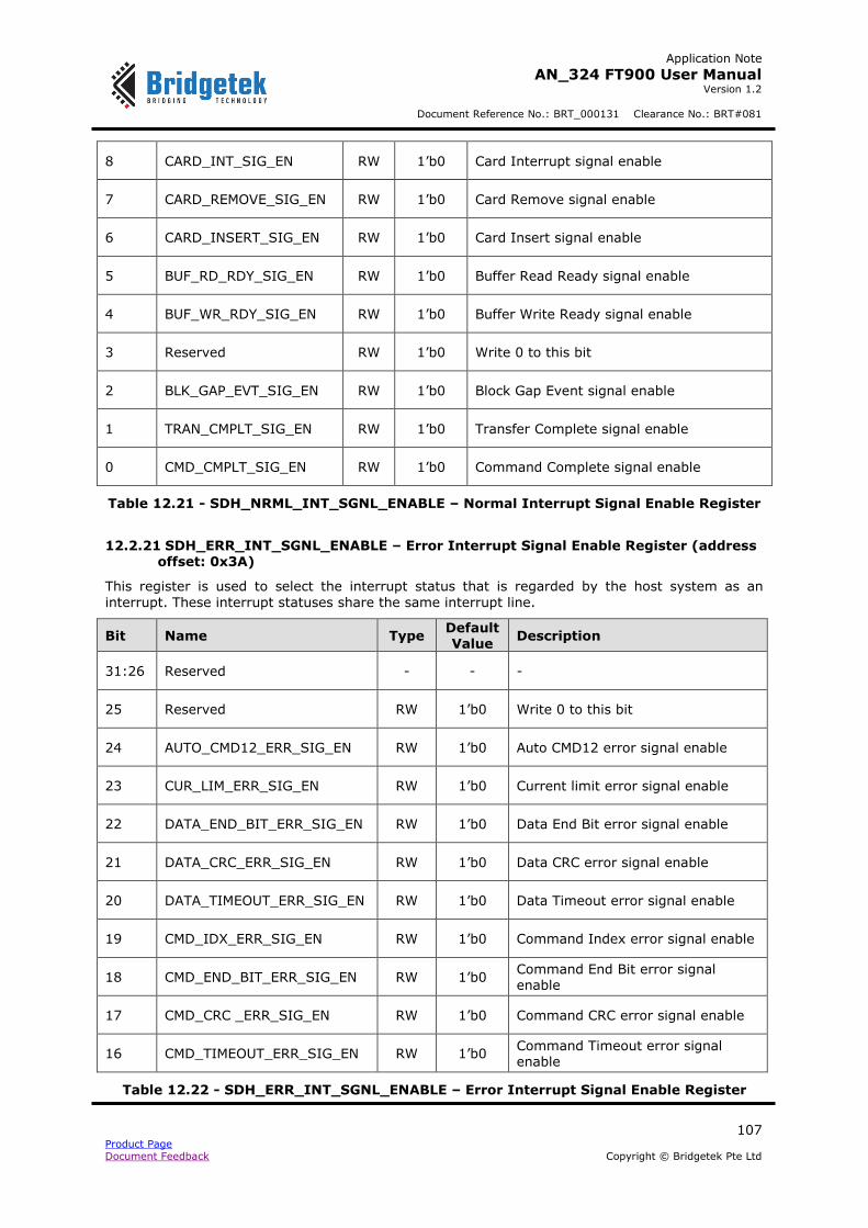
Application Note
AN_324 FT900 User Manual Version 1.2
Document Reference No.: BRT_000131 Clearance No.: BRT#081
107 Product Page Document Feedback Copyright © Bridgetek Pte Ltd
8 CARD_INT_SIG_EN RW 1’b0 Card Interrupt signal enable
7 CARD_REMOVE_SIG_EN RW 1’b0 Card Remove signal enable
6 CARD_INSERT_SIG_EN RW 1’b0 Card Insert signal enable
5 BUF_RD_RDY_SIG_EN RW 1’b0 Buffer Read Ready signal enable
4 BUF_WR_RDY_SIG_EN RW 1’b0 Buffer Write Ready signal enable
3 Reserved RW 1’b0 Write 0 to this bit
2 BLK_GAP_EVT_SIG_EN RW 1’b0 Block Gap Event signal enable
1 TRAN_CMPLT_SIG_EN RW 1’b0 Transfer Complete signal enable
0 CMD_CMPLT_SIG_EN RW 1’b0 Command Complete signal enable
Table 12.21 - SDH_NRML_INT_SGNL_ENABLE – Normal Interrupt Signal Enable Register
12.2.21 SDH_ERR_INT_SGNL_ENABLE – Error Interrupt Signal Enable Register (address offset: 0x3A)
This register is used to select the interrupt status that is regarded by the host system as an
interrupt. These interrupt statuses share the same interrupt line.
Bit Name Type Default Value
Description
31:26 Reserved - - -
25 Reserved RW 1’b0 Write 0 to this bit
24 AUTO_CMD12_ERR_SIG_EN RW 1’b0 Auto CMD12 error signal enable
23 CUR_LIM_ERR_SIG_EN RW 1’b0 Current limit error signal enable
22 DATA_END_BIT_ERR_SIG_EN RW 1’b0 Data End Bit error signal enable
21 DATA_CRC_ERR_SIG_EN RW 1’b0 Data CRC error signal enable
20 DATA_TIMEOUT_ERR_SIG_EN RW 1’b0 Data Timeout error signal enable
19 CMD_IDX_ERR_SIG_EN RW 1’b0 Command Index error signal enable
18 CMD_END_BIT_ERR_SIG_EN RW 1’b0 Command End Bit error signal enable
17 CMD_CRC _ERR_SIG_EN RW 1’b0 Command CRC error signal enable
16 CMD_TIMEOUT_ERR_SIG_EN RW 1’b0 Command Timeout error signal enable
Table 12.22 - SDH_ERR_INT_SGNL_ENABLE – Error Interrupt Signal Enable Register
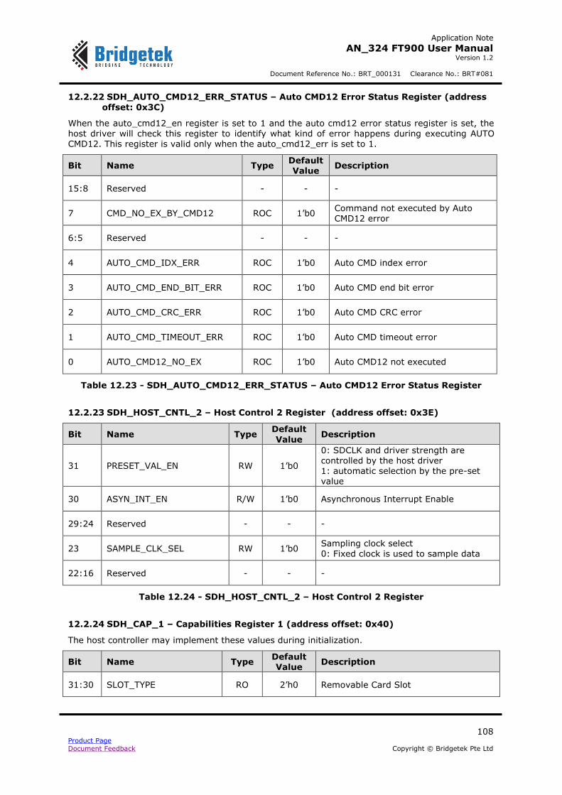
Application Note
AN_324 FT900 User Manual Version 1.2
Document Reference No.: BRT_000131 Clearance No.: BRT#081
108 Product Page Document Feedback Copyright © Bridgetek Pte Ltd
12.2.22 SDH_AUTO_CMD12_ERR_STATUS – Auto CMD12 Error Status Register (address
offset: 0x3C)
When the auto_cmd12_en register is set to 1 and the auto cmd12 error status register is set, the host driver will check this register to identify what kind of error happens during executing AUTO CMD12. This register is valid only when the auto_cmd12_err is set to 1.
Bit Name Type Default Value
Description
15:8 Reserved - - -
7 CMD_NO_EX_BY_CMD12 ROC 1’b0 Command not executed by Auto CMD12 error
6:5 Reserved - - -
4 AUTO_CMD_IDX_ERR ROC 1’b0 Auto CMD index error
3 AUTO_CMD_END_BIT_ERR ROC 1’b0 Auto CMD end bit error
2 AUTO_CMD_CRC_ERR ROC 1’b0 Auto CMD CRC error
1 AUTO_CMD_TIMEOUT_ERR ROC 1’b0 Auto CMD timeout error
0 AUTO_CMD12_NO_EX ROC 1’b0 Auto CMD12 not executed
Table 12.23 - SDH_AUTO_CMD12_ERR_STATUS – Auto CMD12 Error Status Register
12.2.23 SDH_HOST_CNTL_2 – Host Control 2 Register (address offset: 0x3E)
Bit Name Type Default
Value Description
31 PRESET_VAL_EN RW 1’b0
0: SDCLK and driver strength are controlled by the host driver 1: automatic selection by the pre-set value
30 ASYN_INT_EN R/W 1’b0 Asynchronous Interrupt Enable
29:24 Reserved - - -
23 SAMPLE_CLK_SEL RW 1’b0 Sampling clock select 0: Fixed clock is used to sample data
22:16 Reserved - - -
Table 12.24 - SDH_HOST_CNTL_2 – Host Control 2 Register
12.2.24 SDH_CAP_1 – Capabilities Register 1 (address offset: 0x40)
The host controller may implement these values during initialization.
Bit Name Type Default Value
Description
31:30 SLOT_TYPE RO 2’h0 Removable Card Slot
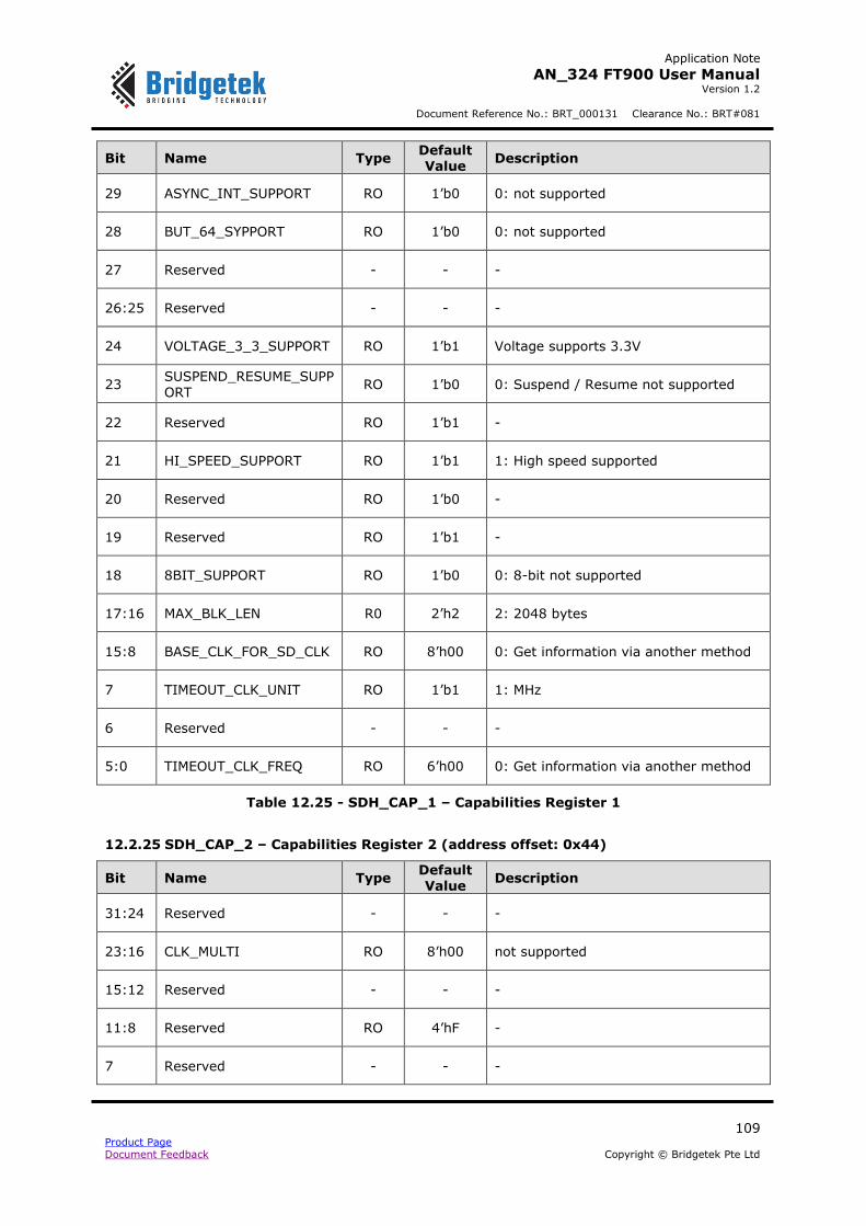
Application Note
AN_324 FT900 User Manual Version 1.2
Document Reference No.: BRT_000131 Clearance No.: BRT#081
109 Product Page Document Feedback Copyright © Bridgetek Pte Ltd
Bit Name Type Default Value
Description
29 ASYNC_INT_SUPPORT RO 1’b0 0: not supported
28 BUT_64_SYPPORT RO 1’b0 0: not supported
27 Reserved - - -
26:25 Reserved - - -
24 VOLTAGE_3_3_SUPPORT RO 1’b1 Voltage supports 3.3V
23 SUSPEND_RESUME_SUPPORT
RO 1’b0 0: Suspend / Resume not supported
22 Reserved RO 1’b1 -
21 HI_SPEED_SUPPORT RO 1’b1 1: High speed supported
20 Reserved RO 1’b0 -
19 Reserved RO 1’b1 -
18 8BIT_SUPPORT RO 1’b0 0: 8-bit not supported
17:16 MAX_BLK_LEN R0 2’h2 2: 2048 bytes
15:8 BASE_CLK_FOR_SD_CLK RO 8’h00 0: Get information via another method
7 TIMEOUT_CLK_UNIT RO 1’b1 1: MHz
6 Reserved - - -
5:0 TIMEOUT_CLK_FREQ RO 6’h00 0: Get information via another method
Table 12.25 - SDH_CAP_1 – Capabilities Register 1
12.2.25 SDH_CAP_2 – Capabilities Register 2 (address offset: 0x44)
Bit Name Type Default Value
Description
31:24 Reserved - - -
23:16 CLK_MULTI RO 8’h00 not supported
15:12 Reserved - - -
11:8 Reserved RO 4’hF -
7 Reserved - - -

Application Note
AN_324 FT900 User Manual Version 1.2
Document Reference No.: BRT_000131 Clearance No.: BRT#081
110 Product Page Document Feedback Copyright © Bridgetek Pte Ltd
Bit Name Type Default Value
Description
6 DRIVER_D_SUPPORT RO 1’b1 not supported
5 DRIVER_C_SUPPORT RO 1’b1 not supported
4 DRIVER_A_SUPPORT RO 1’b1 not supported
3 Reserved - - -
2 DDR50_SUPPORT RO 1’b1 not supported
1 SDR104_SUPPORT RO 1’b0 not supported
0 SDR50_SUPPORT RO 1’b1 not supported
Table 12.26 - SDH_CAP_2 – Capabilities Register 2
12.2.26 SDH_RSRV_1 – Reserved 1 Register (address offset: 0x48)
Bit Name Type Default Value
Description
31:0 Reserved - - -
Table 12.27 - SDH_RSRV_1 – Reserved 1 Register
12.2.27 SDH_RSRV_2 – Reserved 2 Register (address offset: 0x4C)
Bit Name Type Default
Value Description
31:0 Reserved - - -
Table 12.28 - SDH_RSRV_2 – Reserved 2 Register
12.2.28 SDH_FORCE_EVT_CMD_ERR_STATUS – Force Event Register for Auto CMD Error
Status (address offset: 0x50)
The Force Event register is not a physical register. It is an address to which the Auto CMD error status register can be written. The force event register is only for debugging.
Bit Name Type Default Value
Description
15:8 Reserved - - -
7 R_CMD_NO_EX_BY_CMD
12 WO 1’b0
Force event for the Command Not
Executed by Auto CMD12 Error
6:5 Reserved - - -
4 R_CMD_IDX_ERR WO 1’b0 Force event for the Auto CMD Index Error
3 R_CMD_END_BIT_ERR WO 1’b0 Force event for the Auto CMD End Bit Error
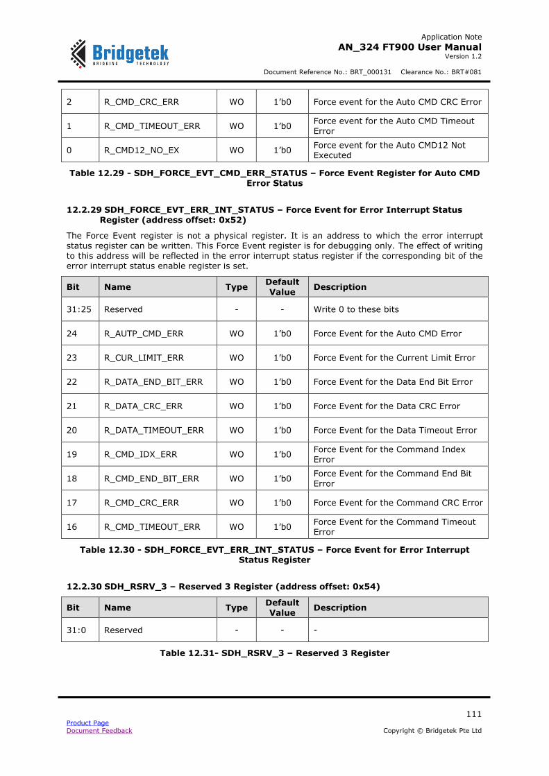
Application Note
AN_324 FT900 User Manual Version 1.2
Document Reference No.: BRT_000131 Clearance No.: BRT#081
111 Product Page Document Feedback Copyright © Bridgetek Pte Ltd
2 R_CMD_CRC_ERR WO 1’b0 Force event for the Auto CMD CRC Error
1 R_CMD_TIMEOUT_ERR WO 1’b0 Force event for the Auto CMD Timeout Error
0 R_CMD12_NO_EX WO 1’b0 Force event for the Auto CMD12 Not Executed
Table 12.29 - SDH_FORCE_EVT_CMD_ERR_STATUS – Force Event Register for Auto CMD Error Status
12.2.29 SDH_FORCE_EVT_ERR_INT_STATUS – Force Event for Error Interrupt Status Register (address offset: 0x52)
The Force Event register is not a physical register. It is an address to which the error interrupt status register can be written. This Force Event register is for debugging only. The effect of writing to this address will be reflected in the error interrupt status register if the corresponding bit of the
error interrupt status enable register is set.
Bit Name Type Default
Value Description
31:25 Reserved - - Write 0 to these bits
24 R_AUTP_CMD_ERR WO 1’b0 Force Event for the Auto CMD Error
23 R_CUR_LIMIT_ERR WO 1’b0 Force Event for the Current Limit Error
22 R_DATA_END_BIT_ERR WO 1’b0 Force Event for the Data End Bit Error
21 R_DATA_CRC_ERR WO 1’b0 Force Event for the Data CRC Error
20 R_DATA_TIMEOUT_ERR WO 1’b0 Force Event for the Data Timeout Error
19 R_CMD_IDX_ERR WO 1’b0 Force Event for the Command Index Error
18 R_CMD_END_BIT_ERR WO 1’b0 Force Event for the Command End Bit Error
17 R_CMD_CRC_ERR WO 1’b0 Force Event for the Command CRC Error
16 R_CMD_TIMEOUT_ERR WO 1’b0 Force Event for the Command Timeout Error
Table 12.30 - SDH_FORCE_EVT_ERR_INT_STATUS – Force Event for Error Interrupt Status Register
12.2.30 SDH_RSRV_3 – Reserved 3 Register (address offset: 0x54)
Bit Name Type Default
Value Description
31:0 Reserved - - -
Table 12.31- SDH_RSRV_3 – Reserved 3 Register
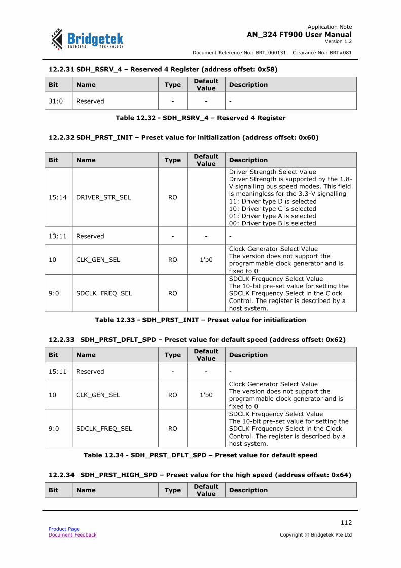
Application Note
AN_324 FT900 User Manual Version 1.2
Document Reference No.: BRT_000131 Clearance No.: BRT#081
112 Product Page Document Feedback Copyright © Bridgetek Pte Ltd
12.2.31 SDH_RSRV_4 – Reserved 4 Register (address offset: 0x58)
Bit Name Type Default Value
Description
31:0 Reserved - - -
Table 12.32 - SDH_RSRV_4 – Reserved 4 Register
12.2.32 SDH_PRST_INIT – Preset value for initialization (address offset: 0x60)
Bit Name Type Default Value
Description
15:14 DRIVER_STR_SEL RO
Driver Strength Select Value Driver Strength is supported by the 1.8-V signalling bus speed modes. This field
is meaningless for the 3.3-V signalling 11: Driver type D is selected 10: Driver type C is selected 01: Driver type A is selected 00: Driver type B is selected
13:11 Reserved - - -
10 CLK_GEN_SEL RO 1’b0
Clock Generator Select Value The version does not support the programmable clock generator and is fixed to 0
9:0 SDCLK_FREQ_SEL RO
SDCLK Frequency Select Value The 10-bit pre-set value for setting the SDCLK Frequency Select in the Clock Control. The register is described by a host system.
Table 12.33 - SDH_PRST_INIT – Preset value for initialization
12.2.33 SDH_PRST_DFLT_SPD – Preset value for default speed (address offset: 0x62)
Bit Name Type Default Value
Description
15:11 Reserved - - -
10 CLK_GEN_SEL RO 1’b0
Clock Generator Select Value The version does not support the programmable clock generator and is fixed to 0
9:0 SDCLK_FREQ_SEL RO
SDCLK Frequency Select Value
The 10-bit pre-set value for setting the SDCLK Frequency Select in the Clock Control. The register is described by a
host system.
Table 12.34 - SDH_PRST_DFLT_SPD – Preset value for default speed
12.2.34 SDH_PRST_HIGH_SPD – Preset value for the high speed (address offset: 0x64)
Bit Name Type Default Value
Description
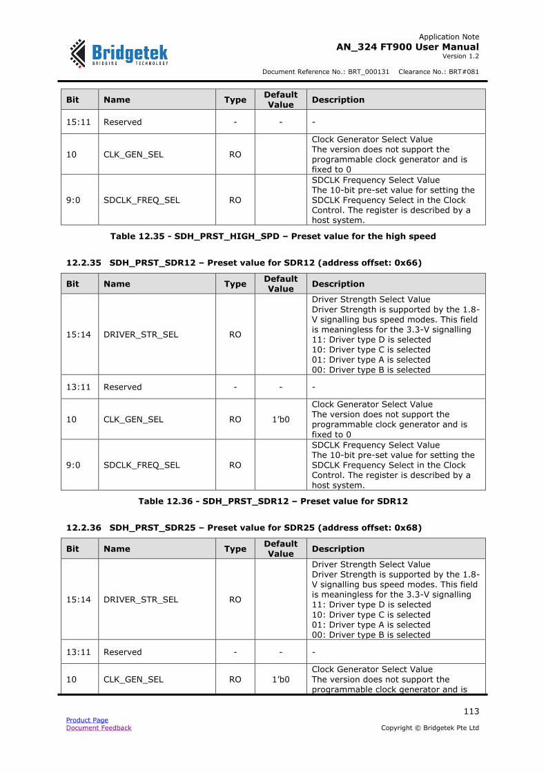
Application Note
AN_324 FT900 User Manual Version 1.2
Document Reference No.: BRT_000131 Clearance No.: BRT#081
113 Product Page Document Feedback Copyright © Bridgetek Pte Ltd
Bit Name Type Default Value
Description
15:11 Reserved - - -
10 CLK_GEN_SEL RO
Clock Generator Select Value The version does not support the programmable clock generator and is fixed to 0
9:0 SDCLK_FREQ_SEL RO
SDCLK Frequency Select Value The 10-bit pre-set value for setting the SDCLK Frequency Select in the Clock Control. The register is described by a host system.
Table 12.35 - SDH_PRST_HIGH_SPD – Preset value for the high speed
12.2.35 SDH_PRST_SDR12 – Preset value for SDR12 (address offset: 0x66)
Bit Name Type Default Value
Description
15:14 DRIVER_STR_SEL RO
Driver Strength Select Value
Driver Strength is supported by the 1.8-V signalling bus speed modes. This field is meaningless for the 3.3-V signalling 11: Driver type D is selected 10: Driver type C is selected 01: Driver type A is selected
00: Driver type B is selected
13:11 Reserved - - -
10 CLK_GEN_SEL RO 1’b0
Clock Generator Select Value The version does not support the programmable clock generator and is
fixed to 0
9:0 SDCLK_FREQ_SEL RO
SDCLK Frequency Select Value The 10-bit pre-set value for setting the SDCLK Frequency Select in the Clock Control. The register is described by a
host system.
Table 12.36 - SDH_PRST_SDR12 – Preset value for SDR12
12.2.36 SDH_PRST_SDR25 – Preset value for SDR25 (address offset: 0x68)
Bit Name Type Default Value
Description
15:14 DRIVER_STR_SEL RO
Driver Strength Select Value Driver Strength is supported by the 1.8-V signalling bus speed modes. This field is meaningless for the 3.3-V signalling
11: Driver type D is selected
10: Driver type C is selected 01: Driver type A is selected 00: Driver type B is selected
13:11 Reserved - - -
10 CLK_GEN_SEL RO 1’b0
Clock Generator Select Value
The version does not support the programmable clock generator and is
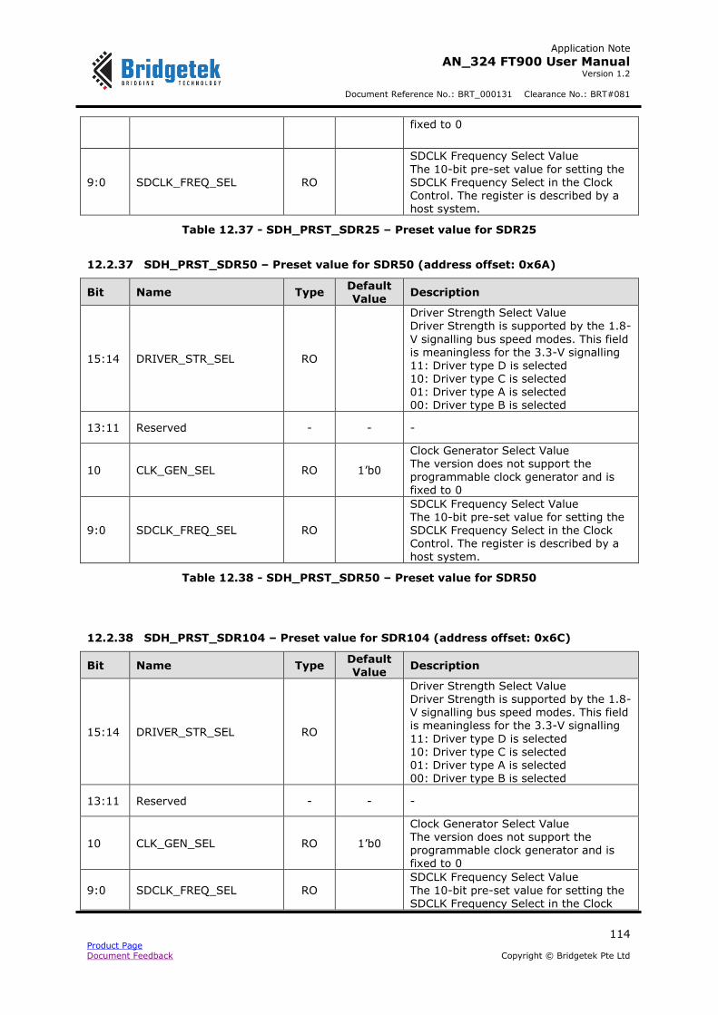
Application Note
AN_324 FT900 User Manual Version 1.2
Document Reference No.: BRT_000131 Clearance No.: BRT#081
114 Product Page Document Feedback Copyright © Bridgetek Pte Ltd
fixed to 0
9:0 SDCLK_FREQ_SEL RO
SDCLK Frequency Select Value
The 10-bit pre-set value for setting the SDCLK Frequency Select in the Clock Control. The register is described by a host system.
Table 12.37 - SDH_PRST_SDR25 – Preset value for SDR25
12.2.37 SDH_PRST_SDR50 – Preset value for SDR50 (address offset: 0x6A)
Bit Name Type Default Value
Description
15:14 DRIVER_STR_SEL RO
Driver Strength Select Value Driver Strength is supported by the 1.8-
V signalling bus speed modes. This field is meaningless for the 3.3-V signalling 11: Driver type D is selected 10: Driver type C is selected 01: Driver type A is selected 00: Driver type B is selected
13:11 Reserved - - -
10 CLK_GEN_SEL RO 1’b0
Clock Generator Select Value The version does not support the programmable clock generator and is fixed to 0
9:0 SDCLK_FREQ_SEL RO
SDCLK Frequency Select Value The 10-bit pre-set value for setting the SDCLK Frequency Select in the Clock Control. The register is described by a host system.
Table 12.38 - SDH_PRST_SDR50 – Preset value for SDR50
12.2.38 SDH_PRST_SDR104 – Preset value for SDR104 (address offset: 0x6C)
Bit Name Type Default Value
Description
15:14 DRIVER_STR_SEL RO
Driver Strength Select Value Driver Strength is supported by the 1.8-V signalling bus speed modes. This field is meaningless for the 3.3-V signalling
11: Driver type D is selected 10: Driver type C is selected 01: Driver type A is selected 00: Driver type B is selected
13:11 Reserved - - -
10 CLK_GEN_SEL RO 1’b0
Clock Generator Select Value The version does not support the programmable clock generator and is fixed to 0
9:0 SDCLK_FREQ_SEL RO
SDCLK Frequency Select Value
The 10-bit pre-set value for setting the SDCLK Frequency Select in the Clock
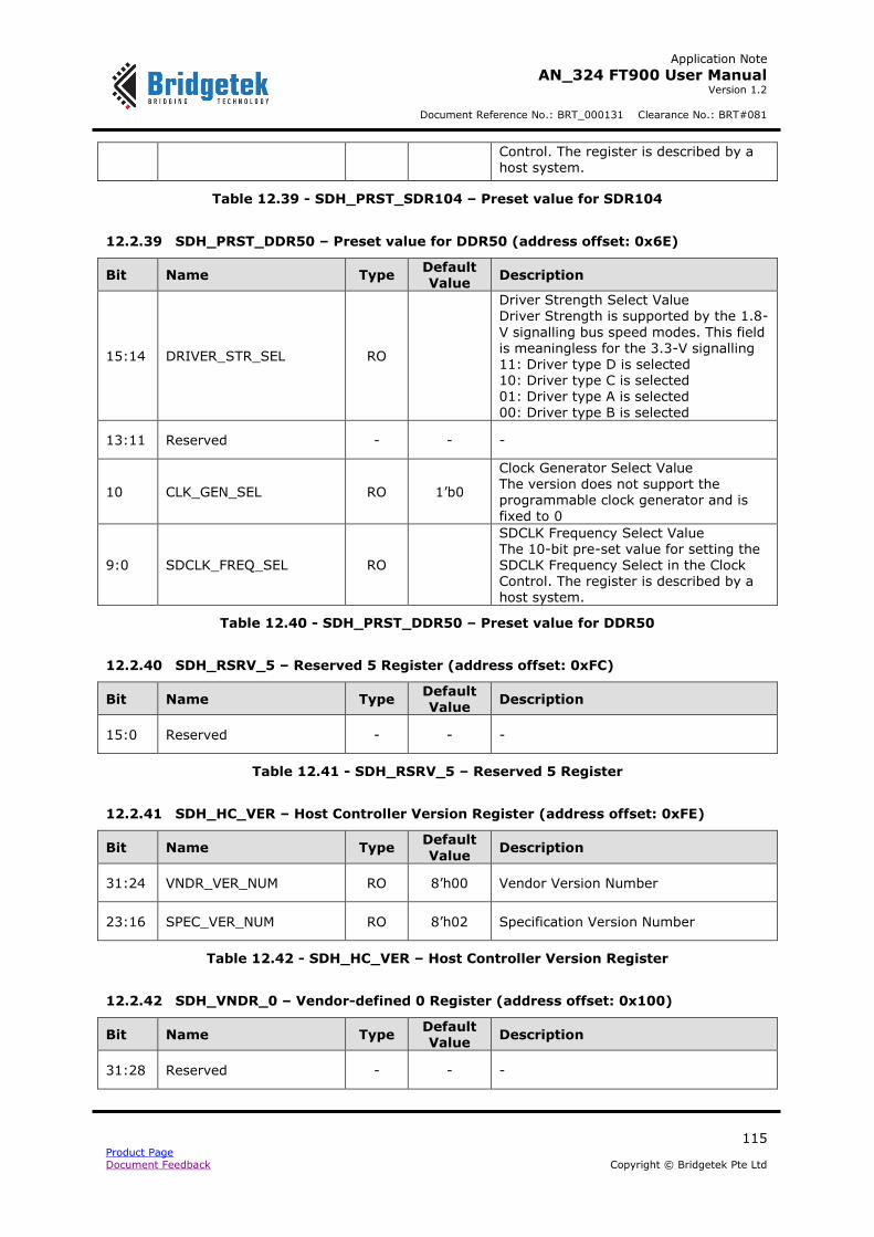
Application Note
AN_324 FT900 User Manual Version 1.2
Document Reference No.: BRT_000131 Clearance No.: BRT#081
115 Product Page Document Feedback Copyright © Bridgetek Pte Ltd
Control. The register is described by a host system.
Table 12.39 - SDH_PRST_SDR104 – Preset value for SDR104
12.2.39 SDH_PRST_DDR50 – Preset value for DDR50 (address offset: 0x6E)
Bit Name Type Default Value
Description
15:14 DRIVER_STR_SEL RO
Driver Strength Select Value Driver Strength is supported by the 1.8-
V signalling bus speed modes. This field is meaningless for the 3.3-V signalling 11: Driver type D is selected 10: Driver type C is selected 01: Driver type A is selected
00: Driver type B is selected
13:11 Reserved - - -
10 CLK_GEN_SEL RO 1’b0
Clock Generator Select Value The version does not support the programmable clock generator and is fixed to 0
9:0 SDCLK_FREQ_SEL RO
SDCLK Frequency Select Value The 10-bit pre-set value for setting the SDCLK Frequency Select in the Clock Control. The register is described by a host system.
Table 12.40 - SDH_PRST_DDR50 – Preset value for DDR50
12.2.40 SDH_RSRV_5 – Reserved 5 Register (address offset: 0xFC)
Bit Name Type Default Value
Description
15:0 Reserved - - -
Table 12.41 - SDH_RSRV_5 – Reserved 5 Register
12.2.41 SDH_HC_VER – Host Controller Version Register (address offset: 0xFE)
Bit Name Type Default
Value Description
31:24 VNDR_VER_NUM RO 8’h00 Vendor Version Number
23:16 SPEC_VER_NUM RO 8’h02 Specification Version Number
Table 12.42 - SDH_HC_VER – Host Controller Version Register
12.2.42 SDH_VNDR_0 – Vendor-defined 0 Register (address offset: 0x100)
Bit Name Type Default Value
Description
31:28 Reserved - - -
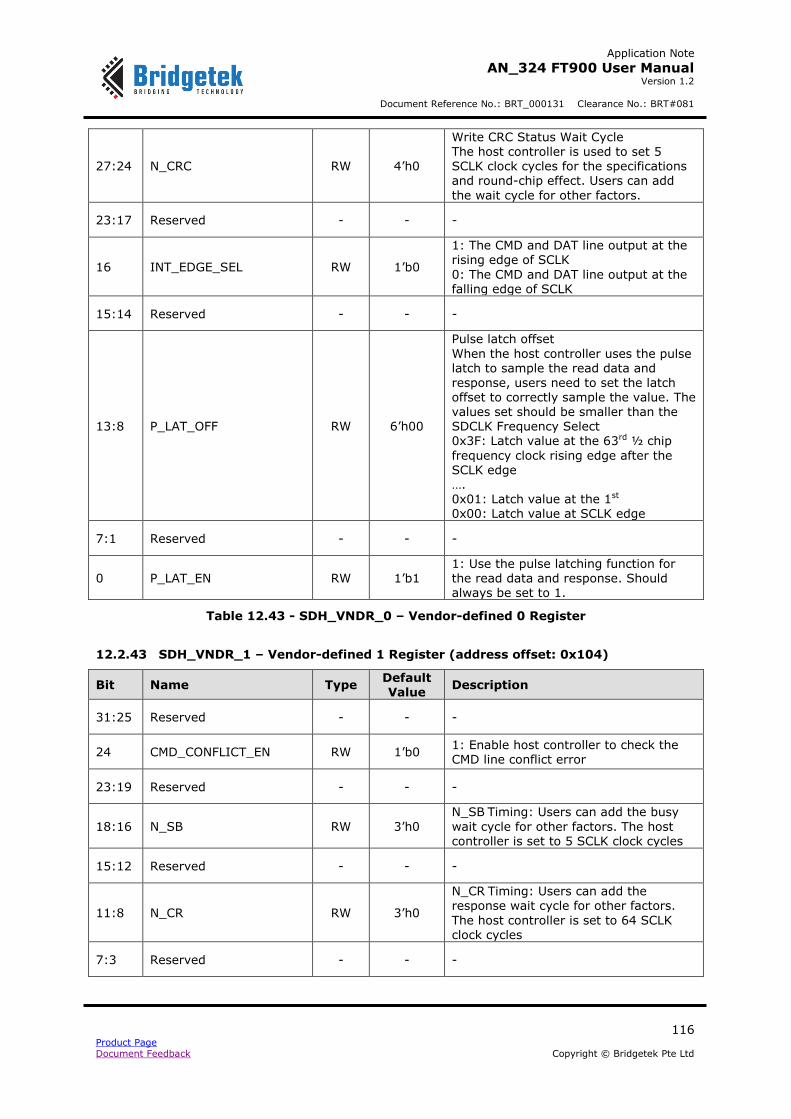
Application Note
AN_324 FT900 User Manual Version 1.2
Document Reference No.: BRT_000131 Clearance No.: BRT#081
116 Product Page Document Feedback Copyright © Bridgetek Pte Ltd
27:24 N_CRC RW 4’h0
Write CRC Status Wait Cycle The host controller is used to set 5 SCLK clock cycles for the specifications and round-chip effect. Users can add
the wait cycle for other factors.
23:17 Reserved - - -
16 INT_EDGE_SEL RW 1’b0
1: The CMD and DAT line output at the rising edge of SCLK
0: The CMD and DAT line output at the falling edge of SCLK
15:14 Reserved - - -
13:8 P_LAT_OFF RW 6’h00
Pulse latch offset
When the host controller uses the pulse latch to sample the read data and
response, users need to set the latch offset to correctly sample the value. The values set should be smaller than the SDCLK Frequency Select 0x3F: Latch value at the 63rd ½ chip
frequency clock rising edge after the SCLK edge …. 0x01: Latch value at the 1st
0x00: Latch value at SCLK edge
7:1 Reserved - - -
0 P_LAT_EN RW 1’b1 1: Use the pulse latching function for the read data and response. Should always be set to 1.
Table 12.43 - SDH_VNDR_0 – Vendor-defined 0 Register
12.2.43 SDH_VNDR_1 – Vendor-defined 1 Register (address offset: 0x104)
Bit Name Type Default Value
Description
31:25 Reserved - - -
24 CMD_CONFLICT_EN RW 1’b0 1: Enable host controller to check the CMD line conflict error
23:19 Reserved - - -
18:16 N_SB RW 3’h0
N_SB Timing: Users can add the busy
wait cycle for other factors. The host controller is set to 5 SCLK clock cycles
15:12 Reserved - - -
11:8 N_CR RW 3’h0
N_CR Timing: Users can add the response wait cycle for other factors.
The host controller is set to 64 SCLK clock cycles
7:3 Reserved - - -
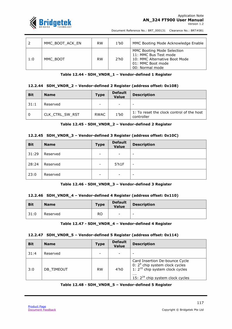
Application Note
AN_324 FT900 User Manual Version 1.2
Document Reference No.: BRT_000131 Clearance No.: BRT#081
117 Product Page Document Feedback Copyright © Bridgetek Pte Ltd
2 MMC_BOOT_ACK_EN RW 1’b0 MMC Booting Mode Acknowledge Enable
1:0 MMC_BOOT RW 2’h0
MMC Booting Mode Selection
11: MMC Bus Test mode 10: MMC Alternative Boot Mode 01: MMC Boot mode 00: Normal mode
Table 12.44 - SDH_VNDR_1 – Vendor-defined 1 Register
12.2.44 SDH_VNDR_2 – Vendor-defined 2 Register (address offset: 0x108)
Bit Name Type Default Value
Description
31:1 Reserved - - -
0 CLK_CTRL_SW_RST RWAC 1’b0 1: To reset the clock control of the host
controller
Table 12.45 - SDH_VNDR_2 – Vendor-defined 2 Register
12.2.45 SDH_VNDR_3 – Vendor-defined 3 Register (address offset: 0x10C)
Bit Name Type Default
Value Description
31:29 Reserved - - -
28:24 Reserved - 5’h1F -
23:0 Reserved - - -
Table 12.46 - SDH_VNDR_3 – Vendor-defined 3 Register
12.2.46 SDH_VNDR_4 – Vendor-defined 4 Register (address offset: 0x110)
Bit Name Type Default Value
Description
31:0 Reserved RO - -
Table 12.47 - SDH_VNDR_4 – Vendor-defined 4 Register
12.2.47 SDH_VNDR_5 – Vendor-defined 5 Register (address offset: 0x114)
Bit Name Type Default Value
Description
31:4 Reserved - - -
3:0 DB_TIMEOUT RW 4’h0
Card Insertion De-bounce Cycle
0: 29 chip system clock cycles 1: 210 chip system clock cycles …. 15: 224 chip system clock cycles
Table 12.48 - SDH_VNDR_5 – Vendor-defined 5 Register
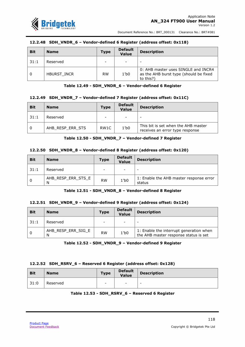
Application Note
AN_324 FT900 User Manual Version 1.2
Document Reference No.: BRT_000131 Clearance No.: BRT#081
118 Product Page Document Feedback Copyright © Bridgetek Pte Ltd
12.2.48 SDH_VNDR_6 – Vendor-defined 6 Register (address offset: 0x118)
Bit Name Type Default Value
Description
31:1 Reserved - - -
0 HBURST_INCR RW 1’b0 0: AHB master uses SINGLE and INCR4 as the AHB burst type (should be fixed to this?)
Table 12.49 - SDH_VNDR_6 – Vendor-defined 6 Register
12.2.49 SDH_VNDR_7 – Vendor-defined 7 Register (address offset: 0x11C)
Bit Name Type Default Value
Description
31:1 Reserved - - -
0 AHB_RESP_ERR_STS RW1C 1’b0 This bit is set when the AHB master receives an error type response
Table 12.50 - SDH_VNDR_7 – Vendor-defined 7 Register
12.2.50 SDH_VNDR_8 – Vendor-defined 8 Register (address offset: 0x120)
Bit Name Type Default Value
Description
31:1 Reserved - - -
0 AHB_RESP_ERR_STS_E
N RW 1’b0
1: Enable the AHB master response error
status
Table 12.51 - SDH_VNDR_8 – Vendor-defined 8 Register
12.2.51 SDH_VNDR_9 – Vendor-defined 9 Register (address offset: 0x124)
Bit Name Type Default Value
Description
31:1 Reserved - - -
0 AHB_RESP_ERR_SIG_EN
RW 1’b0 1: Enable the interrupt generation when the AHB master response status is set
Table 12.52 - SDH_VNDR_9 – Vendor-defined 9 Register
12.2.52 SDH_RSRV_6 – Reserved 6 Register (address offset: 0x128)
Bit Name Type Default
Value Description
31:0 Reserved - - -
Table 12.53 - SDH_RSRV_6 – Reserved 6 Register
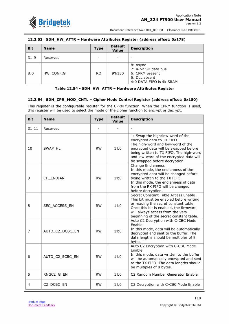
Application Note
AN_324 FT900 User Manual Version 1.2
Document Reference No.: BRT_000131 Clearance No.: BRT#081
119 Product Page Document Feedback Copyright © Bridgetek Pte Ltd
12.2.53 SDH_HW_ATTR – Hardware Attributes Register (address offset: 0x178)
Bit Name Type Default Value
Description
31:9 Reserved - - -
8:0 HW_CONFIG RO 9’h150
8: Async 7: 4-bit SD data bus 6: CPRM present 5: DLL absent
4:0 DATA FIFO is 4k SRAM
Table 12.54 - SDH_HW_ATTR – Hardware Attributes Register
12.2.54 SDH_CPR_MOD_CNTL – Cipher Mode Control Register (address offset: 0x180)
This register is the configurable register for the CPRM function. When the CPRM function is used,
this register will be used to select the mode of the cipher function to encrypt or decrypt.
Bit Name Type Default Value
Description
31:11 Reserved - - -
10 SWAP_HL RW 1’b0
1: Swap the high/low word of the
encrypted data to TX FIFO The high-word and low-word of the encrypted data will be swapped before being written to TX FIFO. The high-word and low-word of the encrypted data will be swapped before decryption.
9 CH_ENDIAN RW 1’b0
Change Endianness In this mode, the endianness of the encrypted data will be changed before being written to the TX FIFO.
In this mode, the endianness of data from the RX FIFO will be changed
before decryption.
8 SEC_ACCESS_EN RW 1’b0
Secret Constant Table Access Enable This bit must be enabled before writing or reading the secret constant table. Once this bit is enabled, the firmware
will always access from the very beginning of the secret constant table.
7 AUTO_C2_DCBC_EN RW 1’b0
Auto C2 Decryption with C-CBC Mode Enable In this mode, data will be automatically decrypted and sent to the buffer. The
data lengths should be multiples of 8 bytes.
6 AUTO_C2_ECBC_EN RW 1’b0
Auto C2 Encryption with C-CBC Mode Enable
In this mode, data written to the buffer will be automatically encrypted and sent
to the TX FIFO. The data lengths should be multiples of 8 bytes.
5 RNGC2_G_EN RW 1’b0 C2 Random Number Generator Enable
4 C2_DCBC_EN RW 1’b0 C2 Decryption with C-CBC Mode Enable
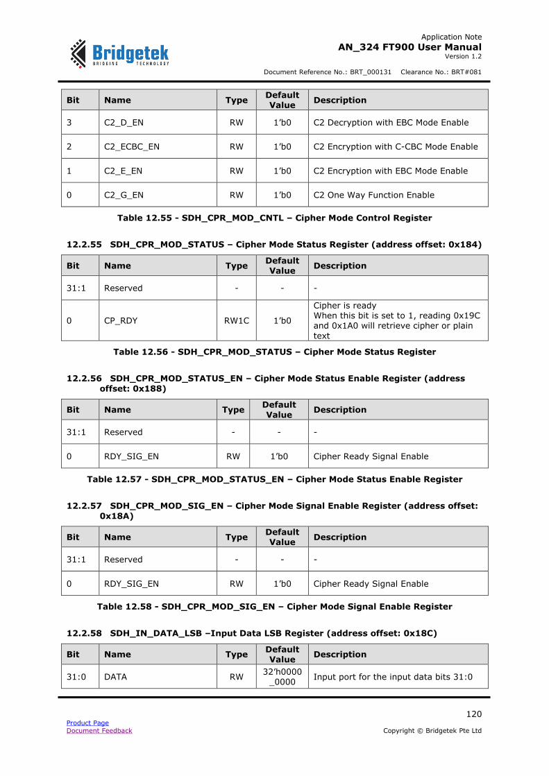
Application Note
AN_324 FT900 User Manual Version 1.2
Document Reference No.: BRT_000131 Clearance No.: BRT#081
120 Product Page Document Feedback Copyright © Bridgetek Pte Ltd
Bit Name Type Default Value
Description
3 C2_D_EN RW 1’b0 C2 Decryption with EBC Mode Enable
2 C2_ECBC_EN RW 1’b0 C2 Encryption with C-CBC Mode Enable
1 C2_E_EN RW 1’b0 C2 Encryption with EBC Mode Enable
0 C2_G_EN RW 1’b0 C2 One Way Function Enable
Table 12.55 - SDH_CPR_MOD_CNTL – Cipher Mode Control Register
12.2.55 SDH_CPR_MOD_STATUS – Cipher Mode Status Register (address offset: 0x184)
Bit Name Type Default Value
Description
31:1 Reserved - - -
0 CP_RDY RW1C 1’b0
Cipher is ready When this bit is set to 1, reading 0x19C and 0x1A0 will retrieve cipher or plain
text
Table 12.56 - SDH_CPR_MOD_STATUS – Cipher Mode Status Register
12.2.56 SDH_CPR_MOD_STATUS_EN – Cipher Mode Status Enable Register (address
offset: 0x188)
Bit Name Type Default
Value Description
31:1 Reserved - - -
0 RDY_SIG_EN RW 1’b0 Cipher Ready Signal Enable
Table 12.57 - SDH_CPR_MOD_STATUS_EN – Cipher Mode Status Enable Register
12.2.57 SDH_CPR_MOD_SIG_EN – Cipher Mode Signal Enable Register (address offset:
0x18A)
Bit Name Type Default Value
Description
31:1 Reserved - - -
0 RDY_SIG_EN RW 1’b0 Cipher Ready Signal Enable
Table 12.58 - SDH_CPR_MOD_SIG_EN – Cipher Mode Signal Enable Register
12.2.58 SDH_IN_DATA_LSB –Input Data LSB Register (address offset: 0x18C)
Bit Name Type Default Value
Description
31:0 DATA RW 32’h0000
_0000 Input port for the input data bits 31:0

Application Note
AN_324 FT900 User Manual Version 1.2
Document Reference No.: BRT_000131 Clearance No.: BRT#081
121 Product Page Document Feedback Copyright © Bridgetek Pte Ltd
Table 12.59 - SDH_IN_DATA_LSB –Input Data LSB Register
12.2.59 SDH_IN_DATA_MSB –Input Data MSB Register (address offset: 0x190)
Bit Name Type Default Value
Description
31:0 DATA RW 32’h0000
_0000 Input port for the input data bits 63:32
Table 12.60 - SDH_IN_DATA_MSB –Input Data MSB Register
12.2.60 SDH_IN_KEY_LSB – Input Key LSB Register (address offset: 0x194)
Bit Name Type Default Value
Description
31:0 KEY RW 32’h0000
_0000 Input port for the input key bits 31:0
Table 12.61 - SDH_IN_KEY_LSB – Input Key LSB Register
12.2.61 SDH_IN_KEY_MSB – Input Key MSB Register (address offset: 0x198)
Bit Name Type Default Value
Description
31:0 KEY RW 32’h0000
_0000 Input port for the input key bits 63:32
Table 12.62 - SDH_IN_KEY_MSB – Input Key MSB Register
12.2.62 SDH_OUT_DATA_LSB – Output Data LSB Register (address offset: 0x19C)
Bit Name Type Default Value
Description
31:0 DATA RW 32’h0000
_0000 Output port for the output data bits 31:0
Table 12.63 - SDH_OUT_DATA_LSB – Output Data LSB Register
12.2.63 SDH_OUT_DATA_MSB – Output Data MSB Register (address offset: 0x1A0)
Bit Name Type Default
Value Description
31:0 DATA RW 32’h0000_
0000 Output port for the output data bits 63:32
Table 12.64 - SDH_OUT_DATA_MSB – Output Data MSB Register
12.2.64 SDH_SCRT_CONS_DATA – Secret Constant Table Data Port (address offset:
0x1A4)
Bit Name Type Default Value
Description
31:8 Reserved - - -
7:0 DATA_PORT RW 8’h00
Secret constant table data port. 256 bytes are needed; this port should be written 256 times to initialize the secret constant table

Application Note
AN_324 FT900 User Manual Version 1.2
Document Reference No.: BRT_000131 Clearance No.: BRT#081
122 Product Page Document Feedback Copyright © Bridgetek Pte Ltd
Table 12.65 - SDH_SCRT_CONS_DATA – Secret Constant Table Data Port

Application Note
AN_324 FT900 User Manual Version 1.2
Document Reference No.: BRT_000131 Clearance No.: BRT#081
123 Product Page Document Feedback Copyright © Bridgetek Pte Ltd
13 UART
The device supports 2 UARTs with the following features:
Software compatible with 450, 550, 750 and 950 UARTs
Separate configurable BAUD clock line
Configuration capability
Two modes of operation: UART mode and FIFO mode
Majority voting logic
16 / 128 bytes FIFO for TX and RX in FIFO mode to reduce the interrupt frequency
adds or deletes standard asynchronous communication bits (start, stop and parity) to or
from the serial data
Double buffering for both TX and RX in UART mode
Independently controlled transmit, receive, line status and data set interrupts
Programmable baud generator
MODEM control functions (CTS, RTS, DSR, DTR, RI and DCD)
Programmable automatic out-of-band Flow Control logic through Auto-RTS and Auto-CTS
Programmable automatic Flow Control logic using DTR and DSR
Programmable automatic in-band Flow Control logic using XON / XOFF characters
Programmable special characters detection
Trigger levels for TX and RX FIFO interrupts, automatic in-band and out-of-band flow
control
RS-485 buffer enable signals
TX and RX disable capability
Fully programmable serial interface characteristics:
o 5-, 6-, 7-, 8- or 9-bit characters
o Even, odd, or no-parity bit generation and detection
o 1-, 1.5, or 2-stop bit generation
o Baud generation
o Detection of bad data in receive FIFO
Clock prescaler from 1 to 31875
Enhanced isochronous clock option

Application Note
AN_324 FT900 User Manual Version 1.2
Document Reference No.: BRT_000131 Clearance No.: BRT#081
124 Product Page Document Feedback Copyright © Bridgetek Pte Ltd
Complete status reporting capabilities
False start bit detection
Line-break generation and detection. Internal diagnostic capabilities:
o Loop-back controls for communications link fault isolation
o Break, parity, overrun, framing error simulation
Full prioritised interrupt system controls
Software reset
13.1 Register Summary
The registers offset from the base addresses are 0x10320 for UART 1 and 0x10330 for UART 2. All registers can only be accessed via Byte (8-bit) mode.
Offset Register Default value
References
STANDARD 550 COMPATIBLE REGISTERS
0x00 UART_RBR - Receiver Buffer Register 0x00 Section 13.3.1
0x00 UART_THR - Transmitter Holding Register 0x00 Section 13.3.2
0x00 UART_DIV_LSB - Divisor LSB Register 0x00 Section 13.3.3
0x01 UART_DIV_MSB - Divisor MSB Register 0x00 Section 13.3.4
0x01 UART_INT_ENABLE - Interrupt Enable Register 0x00 Section 13.3.5
0x02 UART_INT_STATUS - Interrupt Status Register 0x00 Section 13.3.6
0x02 UART_FCR FIFO - Control Register 0x00 Section 13.3.7
0x03 UART_LCR Line - Control Register 0x00 Section 13.3.8
0x04 UART_MCR - Modem Control Register 0x00 Section 13.3.9
0x05 UART_LSR - Line Status Register 0x00 Section 13.3.10
0x06 UART_MSR - Modem Status Register 0x00 Section 13.3.11
0x07 UART_SPR - SPR Register 0x00 Section 13.3.12
650 COMPATIBLE REGISTERS
0x02 UART_EFR - Enhanced Feature Register 0x00 Section 13.4.1
0x04 UART_XON1 - XON1 Register 0x00 Section 13.4.2
0x05 UART_XON2 - XON2 Register 0x00 Section 13.4.3
0x06 UART_XOFF1 - XOFF1 Register 0x00 Section 13.4.4
0x07 UART_XOFF2 - XOFF2 Register 0x00 Section 13.4.5
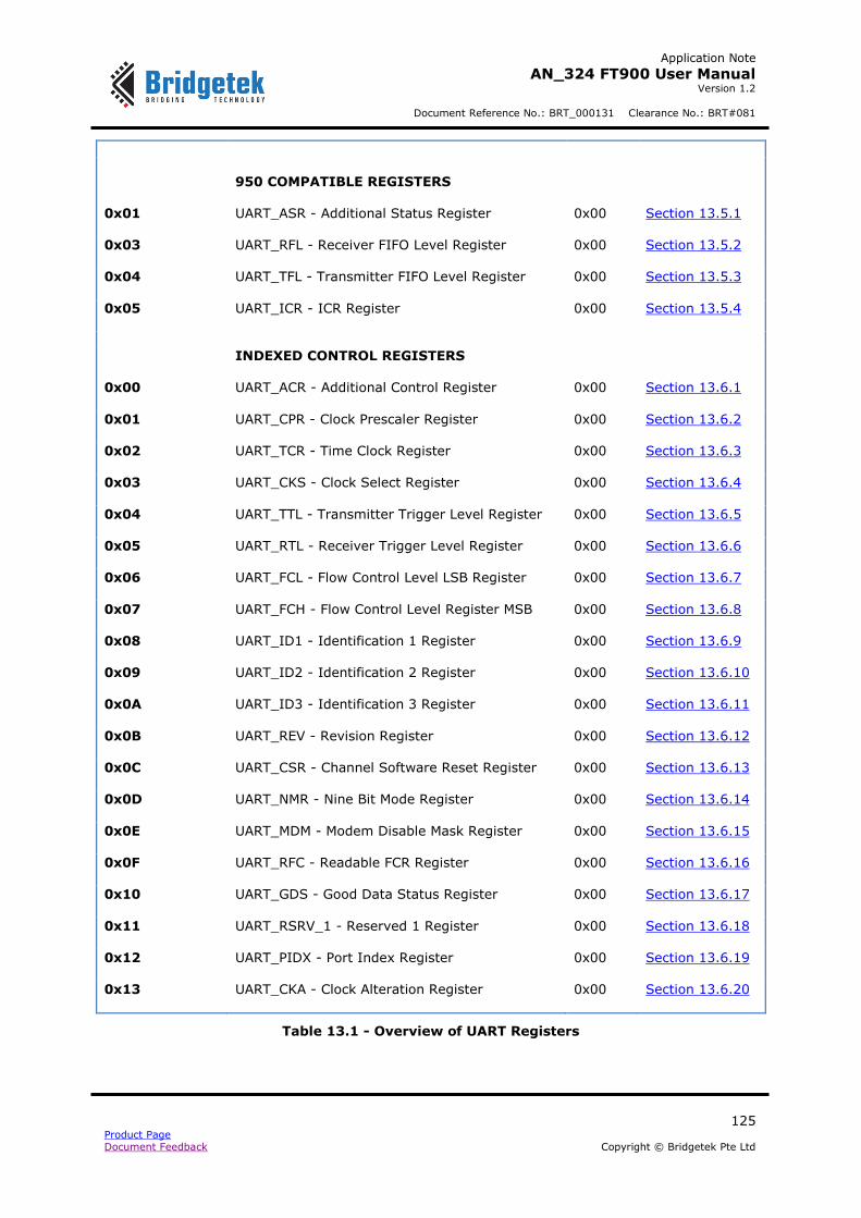
Application Note
AN_324 FT900 User Manual Version 1.2
Document Reference No.: BRT_000131 Clearance No.: BRT#081
125 Product Page Document Feedback Copyright © Bridgetek Pte Ltd
950 COMPATIBLE REGISTERS
0x01 UART_ASR - Additional Status Register 0x00 Section 13.5.1
0x03 UART_RFL - Receiver FIFO Level Register 0x00 Section 13.5.2
0x04 UART_TFL - Transmitter FIFO Level Register 0x00 Section 13.5.3
0x05 UART_ICR - ICR Register 0x00 Section 13.5.4
INDEXED CONTROL REGISTERS
0x00 UART_ACR - Additional Control Register 0x00 Section 13.6.1
0x01 UART_CPR - Clock Prescaler Register 0x00 Section 13.6.2
0x02 UART_TCR - Time Clock Register 0x00 Section 13.6.3
0x03 UART_CKS - Clock Select Register 0x00 Section 13.6.4
0x04 UART_TTL - Transmitter Trigger Level Register 0x00 Section 13.6.5
0x05 UART_RTL - Receiver Trigger Level Register 0x00 Section 13.6.6
0x06 UART_FCL - Flow Control Level LSB Register 0x00 Section 13.6.7
0x07 UART_FCH - Flow Control Level Register MSB 0x00 Section 13.6.8
0x08 UART_ID1 - Identification 1 Register 0x00 Section 13.6.9
0x09 UART_ID2 - Identification 2 Register 0x00 Section 13.6.10
0x0A UART_ID3 - Identification 3 Register 0x00 Section 13.6.11
0x0B UART_REV - Revision Register 0x00 Section 13.6.12
0x0C UART_CSR - Channel Software Reset Register 0x00 Section 13.6.13
0x0D UART_NMR - Nine Bit Mode Register 0x00 Section 13.6.14
0x0E UART_MDM - Modem Disable Mask Register 0x00 Section 13.6.15
0x0F UART_RFC - Readable FCR Register 0x00 Section 13.6.16
0x10 UART_GDS - Good Data Status Register 0x00 Section 13.6.17
0x11 UART_RSRV_1 - Reserved 1 Register 0x00 Section 13.6.18
0x12 UART_PIDX - Port Index Register 0x00 Section 13.6.19
0x13 UART_CKA - Clock Alteration Register 0x00 Section 13.6.20
Table 13.1 - Overview of UART Registers
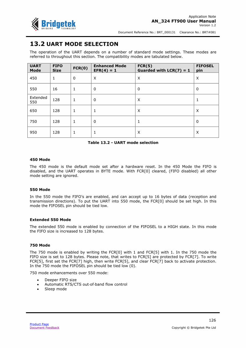
Application Note
AN_324 FT900 User Manual Version 1.2
Document Reference No.: BRT_000131 Clearance No.: BRT#081
126 Product Page Document Feedback Copyright © Bridgetek Pte Ltd
13.2 UART MODE SELECTION
The operation of the UART depends on a number of standard mode settings. These modes are referred to throughout this section. The compatibility modes are tabulated below.
UART Mode
FIFO Size
FCR(0) Enhanced Mode EFR(4) = 1
FCR(5) Guarded with LCR(7) = 1
FIFOSEL pin
450 1 0 X X X
550 16 1 0 0 0
Extended 550
128 1 0 X 1
650 128 1 1 X X
750 128 1 0 1 0
950 128 1 1 X X
Table 13.2 - UART mode selection
450 Mode
The 450 mode is the default mode set after a hardware reset. In the 450 Mode the FIFO is disabled, and the UART operates in BYTE mode. With FCR[0] cleared, (FIFO disabled) all other mode setting are ignored.
550 Mode
In the 550 mode the FIFO’s are enabled, and can accept up to 16 bytes of data (reception and transmission directions). To put the UART into 550 mode, the FCR[0] should be set high. In this mode the FIFOSEL pin should be tied low.
Extended 550 Mode
The extended 550 mode is enabled by connection of the FIFOSEL to a HIGH state. In this mode the FIFO size is increased to 128 bytes.
750 Mode
The 750 mode is enabled by writing the FCR[0] with 1 and FCR[5] with 1. In the 750 mode the FIFO size is set to 128 bytes. Please note, that writes to FCR[5] are protected by FCR[7]. To write FCR[5], first set the FCR[7] high, then write FCR[5], and clear FCR[7] back to activate protection. In the 750 mode the FIFOSEL pin should be tied low (0).
750 mode enhancements over 550 mode:
Deeper FIFO size Automatic RTS/CTS out‐of‐band flow control
Sleep mode
Application Note
AN_324 FT900 User Manual Version 1.2
Document Reference No.: BRT_000131 Clearance No.: BRT#081
127 Product Page Document Feedback Copyright © Bridgetek Pte Ltd
650 Mode
The 650 mode is active when EFR[4] is set (enhanced mode is enabled). As 650 software drivers usually put the device into enhanced mode, running 650 drivers on the UART device will result in 650 compatibility with 128 deep FIFO’s, as long as FCR[0] is set.
The FIFOSEL state is ignored in the 650 mode.
The 650 mode enhancements over 550 mode:
Deeper FIFO size Automatic RTS/CTS out‐of‐band flow control
Sleep mode Automatic in‐bank flow control
Special character detection IRDA‐format transmit and receive mode
Transmit trigger levels
Optional clock prescaler
950 Mode
The additional features of 950 mode apply only when UART is in Enhanced mode (EFR[4] = 1). FCR[0] set in Enhanced mode enables the 128 Bytes FIFO mode.
Configuration of the UART in 950 Mode is identical with the 650 Mode. Additional specific features
of 950 Mode‘s, are enabled using the Additional Control Register ACR. In addition to larger FIFO’s, higher baud rates the enhancements of 950 over 650 mode are:
Selectable arbitrary trigger levels for the receiver and transmitter FIFO interrupts Improved automatic flow control using selectable arbitrary thresholds DSR/DTR automatic flow control Transmitter and receiver can be optionally disabled
Software reset of device Readable FIFO fill levels Optional generation of an RS‐485 buffer enable signal
Four‐byte device identification
Readable status for automatic in‐band and out‐of‐band flow control
External 1x clock modes Flexible M N/8 clock prescaler 9‐bit data mode
The 950 trigger levels are enabled when ACR[5] is set (FCR[7:4] are ignored). The arbitrary trigger levels can be defined in RTL, TTL, FCL and FCH registers. The Additional Status Register (ASR) offers flow control status for the local and remote transmitters. FIFO levels are readable using RFL and TFL registers.
The user may apply an external 1x (or Nx) clock for the transmitter and receiver to the RI and DSR pin respectively. The transmitter clock may be asserted on the DTR pin. The external clock options are selected through the CKS register.
It is also possible to define the over‐sampling rate used by the transmitter and receiver clocks. The
450/550/750 and compatible devices employ 16 times over‐sampling . There are 16 clock cycles
per bit. The UART can employ over‐sampling rate from 4 to 16 by programming the TCR register.
This allows the data rates to be increased. Default value after reset for this register is 0x00, which corresponds to a 16 cycle sampling clock. Writing 0x01, 0x02 or 0x03 will also result in 16 cycle sampling clock. To program the value to any value from 4 to 15 it is necessary to write this value into TCR, to set the device to a 13 cycle sampling clock it would be necessary to write 0x0D to TCR.
The UART also offers 9‐bit data frames for multi‐drop industrial applications.
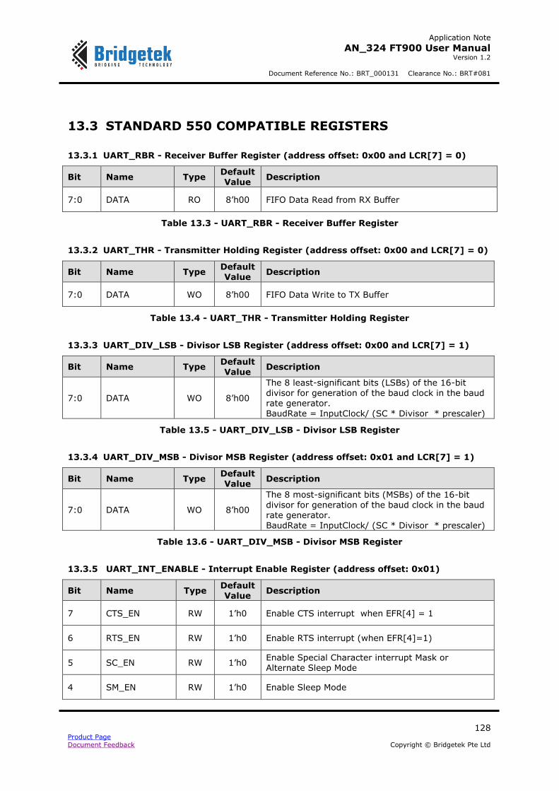
Application Note
AN_324 FT900 User Manual Version 1.2
Document Reference No.: BRT_000131 Clearance No.: BRT#081
128 Product Page Document Feedback Copyright © Bridgetek Pte Ltd
13.3 STANDARD 550 COMPATIBLE REGISTERS
13.3.1 UART_RBR - Receiver Buffer Register (address offset: 0x00 and LCR[7] = 0)
Bit Name Type Default Value
Description
7:0 DATA RO 8’h00 FIFO Data Read from RX Buffer
Table 13.3 - UART_RBR - Receiver Buffer Register
13.3.2 UART_THR - Transmitter Holding Register (address offset: 0x00 and LCR[7] = 0)
Bit Name Type Default Value
Description
7:0 DATA WO 8’h00 FIFO Data Write to TX Buffer
Table 13.4 - UART_THR - Transmitter Holding Register
13.3.3 UART_DIV_LSB - Divisor LSB Register (address offset: 0x00 and LCR[7] = 1)
Bit Name Type Default Value
Description
7:0 DATA WO 8’h00
The 8 least-significant bits (LSBs) of the 16-bit divisor for generation of the baud clock in the baud rate generator. BaudRate = InputClock/ (SC * Divisor * prescaler)
Table 13.5 - UART_DIV_LSB - Divisor LSB Register
13.3.4 UART_DIV_MSB - Divisor MSB Register (address offset: 0x01 and LCR[7] = 1)
Bit Name Type Default Value
Description
7:0 DATA WO 8’h00
The 8 most-significant bits (MSBs) of the 16-bit divisor for generation of the baud clock in the baud rate generator. BaudRate = InputClock/ (SC * Divisor * prescaler)
Table 13.6 - UART_DIV_MSB - Divisor MSB Register
13.3.5 UART_INT_ENABLE - Interrupt Enable Register (address offset: 0x01)
Bit Name Type Default Value
Description
7 CTS_EN RW 1’h0 Enable CTS interrupt when EFR[4] = 1
6 RTS_EN RW 1’h0 Enable RTS interrupt (when EFR[4]=1)
5 SC_EN RW 1’h0 Enable Special Character interrupt Mask or Alternate Sleep Mode
4 SM_EN RW 1’h0 Enable Sleep Mode
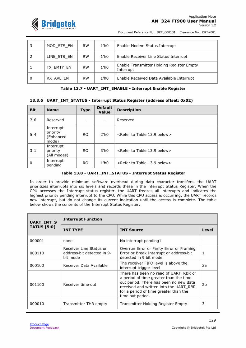
Application Note
AN_324 FT900 User Manual Version 1.2
Document Reference No.: BRT_000131 Clearance No.: BRT#081
129 Product Page Document Feedback Copyright © Bridgetek Pte Ltd
3 MOD_STS_EN RW 1’h0 Enable Modem Status Interrupt
2 LINE_STS_EN RW 1’h0 Enable Receiver Line Status Interrupt
1 TX_EMTY_EN RW 1’h0 Enable Transmitter Holding Register Empty Interrupt
0 RX_AVL_EN RW 1’h0 Enable Received Data Available Interrupt
Table 13.7 - UART_INT_ENABLE - Interrupt Enable Register
13.3.6 UART_INT_STATUS - Interrupt Status Register (address offset: 0x02)
Bit Name Type Default Value
Description
7:6 Reserved - - Reserved
5:4
Interrupt priority (Enhanced mode)
RO 2’h0 <Refer to Table 13.9 below>
3:1
Interrupt
priority (All modes)
RO 3’h0 <Refer to Table 13.9 below>
0 Interrupt pending
RO 1’h0 <Refer to Table 13.9 below>
Table 13.8 - UART_INT_STATUS - Interrupt Status Register
In order to provide minimum software overhead during data character transfers, the UART prioritizes interrupts into six levels and records these in the interrupt Status Register. When the CPU accesses the Interrupt status register, the UART freezes all interrupts and indicates the
highest priority pending interrupt to the CPU. While this CPU access is occurring, the UART records new interrupt, but do not change its current indication until the access is complete. The table
below shows the contents of the Interrupt Status Register.
UART_INT_S
TATUS [5:0]
Interrupt Function
INT TYPE INT Source Level
000001 none No interrupt pending1 ‐
000110
Receiver Line Status or address‐bit detected in 9‐bit mode
Overrun Error or Parity Error or Framing Error or Break Interrupt or address‐bit
detected in 9‐bit mode 1
000100 Receiver Data Available The receiver FIFO level is above the interrupt trigger level
2a
001100 Receiver time‐out
There has been no read of UART_RBR or a period of time greater than the time‐out period. There has been no new data received and written into the UART_RBR for a period of time greater than the time‐out period.
2b
000010 Transmitter THR empty Transmitter Holding Register Empty 3

Application Note
AN_324 FT900 User Manual Version 1.2
Document Reference No.: BRT_000131 Clearance No.: BRT#081
130 Product Page Document Feedback Copyright © Bridgetek Pte Ltd
UART_INT_S
TATUS [5:0]
Interrupt Function
INT TYPE INT Source Level
000000 Modem status change Clear to Send or Data Set Ready or Ring Indicator or Data Carrier Detect
4
010000
In‐band flow control XOFF
or special character (XOFF2) or special character 1,2,3 or 4 or bit 9 set in 9 bit mode
Valid XOFF, valid XOFF2 or matches special character 1,2,3 or 4(only in
Enhanced mode)
5
100000 CTS or RTS change of state When CTS or RTS bits will change 6
Table 13.9 - Interrupt Status Register Software Handling
Notes:
1 – ISR[0] indicates whether any interrupts are pending. 2 ‐ Interrupts of priority levels 5 and 6 cannot occur unless the UART is in Enhanced mode
3 ‐ ISR[5] is only used in 650 & 950 modes. In 750 mode, it is 0 when FIFO size is 16 and 1 when
FIFO size is 128. In all other modes it is permanently set to 0.
13.3.7 UART_FCR - FIFO Control Register (address offset: 0x02)
550 AND 750 MODE
Bit Name Type Default
Value Description
7:6 RCVR_TRIG WO 2’h0 Receiver FIFO Trigger
5 FIFO_SIZE WO 1’h0 Enable UART support for 128 Byte deep FIFO’s
4:3 Reserved WO 2’h0
2 TXMT_RST WO 1’h0
Transmitter FIFO reset. Writing a 1 to FCR2 clears all bytes in the XMIT FIFO and resets its counter logic to 0. The shift register is not cleared. The 1 that is written to this bit position is self‐clearing.
1 RCVR_RST WO 1’h0
Receiver FIFO reset. Writing a 1 to FCR1 clears all bytes in the RCVR FIFO and resets its counter logic to 0. The shift register is not cleared. The 1 that is written to this bit position is self‐clearing.
0 FIFO_EN WO 1’h0 Receiver and Transmitter FIFO’s enable.
Table 13.10 - UART_FCR - FIFO Control Register – 550 mode
This is a write only register at the same location as the ISR (the ISR is a read only register).
Readable contents of this register are placed in ICR space on 0x0F offset. This register is used to enable the FIFOs, clear the FIFOs, set the FIFO triggers levels, and select the type of DMA signaling. When changing from the FIFO Mode to UART Mode and vice versa, data is automatically
cleared from the FIFOs. This bit must be a 1 when other FCR bits are written to or they will not be programmed.
RCVR TRGIGG(1:0) ‐ are used to set the trigger level for the RCVR FIFO interrupt.
Fcr[7:6] RCVR FIFO TRIGGER LEVEL

Application Note
AN_324 FT900 User Manual Version 1.2
Document Reference No.: BRT_000131 Clearance No.: BRT#081
131 Product Page Document Feedback Copyright © Bridgetek Pte Ltd
Fcr[7:6] RCVR FIFO TRIGGER LEVEL
Standard FIFO*mode (16 B) Extended FIFO*mode*(128B)
00 1 1
01 4 32
10 8 64
11 14 112
Table 13.11 - UART_RCVR - FIFO Trigger Level – 550 mode
* ‐ depends on Ext FIFO enable (FCR(5)) bit value
In this mode the transmitter trigger level is equal to 1.
650 MODE
Bit Name Type Default
Value Description
7:6 RCVR_TRIG WO 2’h0 Receiver FIFO Trigger
5:4 THR_TRIG WO 1’h0 Transmitter FIFO Trigger
3 Reserved - 2’h0 -
2 TXMT_RST WO 1’h0
Transmitter FIFO reset. Writing a 1 to FCR2 clears all bytes in the XMIT FIFO and resets its counter logic to 0. The shift register is not cleared. The 1 that is written to this bit position is self‐clearing
1 RCVR_RST WO 1’h0
Receiver FIFO reset. Writing a 1 to FCR1 clears all
bytes in the RCVR FIFO and resets its counter logic to 0. The shift register is not cleared. The 1 that is written to this bit position is self‐clearing
0 FIFO_EN WO 1’h0 Receiver and Transmitter FIFO’s enable
Table 13.12 - UART_FCR - FIFO Control Register – 650 mode
This is a write only register at the same location as the ISR (the ISR is a read only register). This register is used to enable the FIFOs, clear the FIFOs, set the RCVR FIFO and THR FIFO triggers level, and select the type of DMA signaling. When changing from the FIFO Mode to UART Mode and vice versa, data is automatically cleared from the FIFOs. This bit must be a 1 when other FCR bits are written to or they will not be programmed.
RCVR TRGIGG(1:0) ‐ are used to set the trigger level for the RCVR FIFO interrupt and flow control.
FCR[7:6]
RCVR FIFO TRIGGER LEVEL
Lower trigger for flow control
Interrupt trigger and upper trigger for flow control
00 1 16
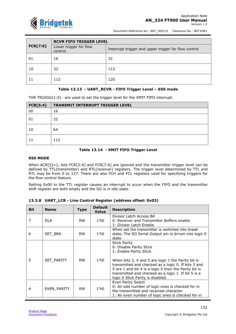
Application Note
AN_324 FT900 User Manual Version 1.2
Document Reference No.: BRT_000131 Clearance No.: BRT#081
132 Product Page Document Feedback Copyright © Bridgetek Pte Ltd
FCR[7:6]
RCVR FIFO TRIGGER LEVEL
Lower trigger for flow control
Interrupt trigger and upper trigger for flow control
01 16 32
10 32 112
11 112 120
Table 13.13 - UART_RCVR - FIFO Trigger Level – 650 mode
THR TRGIGG(1:0) ‐ are used to set the trigger level for the XMIT FIFO interrupt.
FCR[5:4] TRANSMIT INTERRUPT TRIGGER LEVEL
00 16
01 32
10 64
11 112
Table 13.14 - XMIT FIFO Trigger Level
950 MODE
When ACR[5]=1, bits FCR[5:4] and FCR[7:6] are ignored and the transmitter trigger level can be defined by TTL(transmitter) and RTL(receiver) registers. The trigger level determined by TTL and RTL may be from 0 to 127. There are also FCH and FCL registers used for specifying triggers for the flow control feature.
Setting 0x00 to the TTL register causes an interrupt to occur when the FIFO and the transmitter
shift register are both empty and the SO is in idle state.
13.3.8 UART_LCR - Line Control Register (address offset: 0x03)
Bit Name Type Default Value
Description
7 DLA RW 1’h0 Divisor Latch Access Bit 0: Receiver and Transmitter Buffers enable
1: Divisor Latch Enable
6 SET_BRK RW 1’h0 When set the transmitter is switched into break state, The SO Serial Output pin is driven into logic 0 state
5 SET_PARITY RW 1’h0
Stick Parity 0: Disable Parity Stick 1: Enable Parity Stick
When bits 3, 4 and 5 are logic 1 the Parity bit is transmitted and checked as a logic 0. If bits 3 and 5 are 1 and bit 4 is a logic 0 then the Parity bit is transmitted and checked as a logic 1. If bit 5 is a logic 0 Stick Parity is disabled.
4 EVEN_PARITY RW 1’h0
Even Parity Select
0: An odd number of logic ones is checked for in the transmitted and received character 1: An even number of logic ones is checked for in
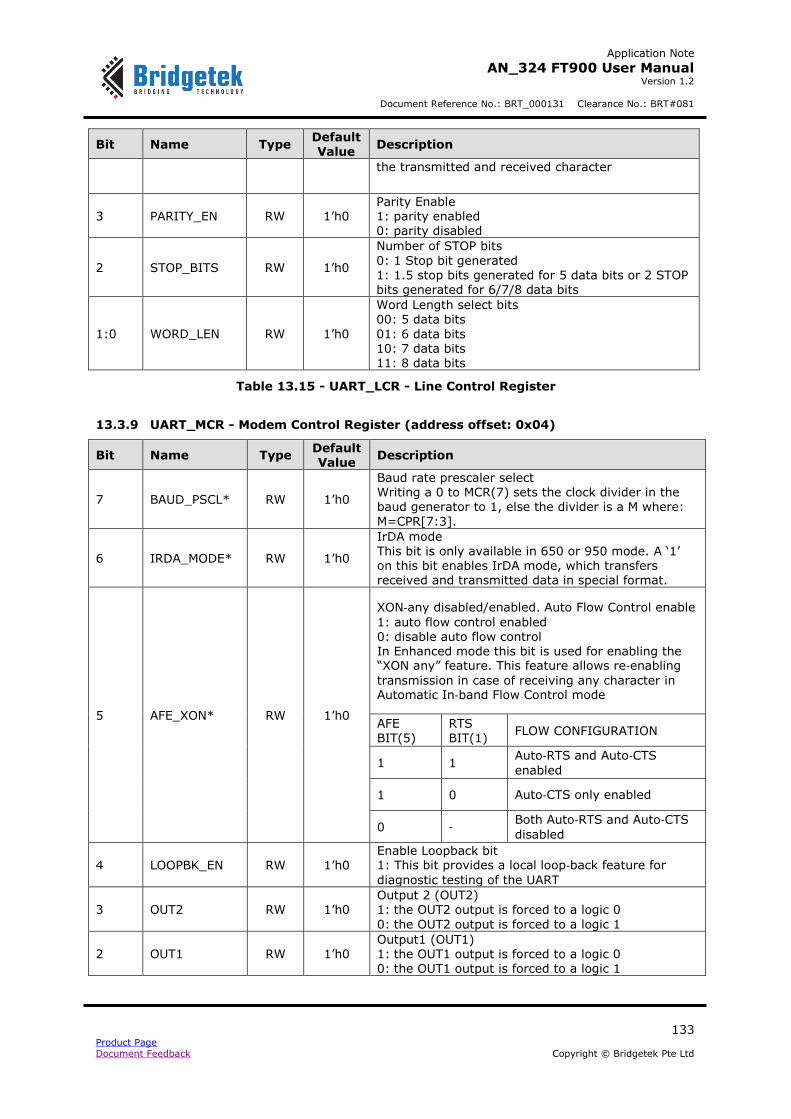
Application Note
AN_324 FT900 User Manual Version 1.2
Document Reference No.: BRT_000131 Clearance No.: BRT#081
133 Product Page Document Feedback Copyright © Bridgetek Pte Ltd
Bit Name Type Default Value
Description
the transmitted and received character
3 PARITY_EN RW 1’h0 Parity Enable 1: parity enabled 0: parity disabled
2 STOP_BITS RW 1’h0
Number of STOP bits
0: 1 Stop bit generated 1: 1.5 stop bits generated for 5 data bits or 2 STOP bits generated for 6/7/8 data bits
1:0 WORD_LEN RW 1’h0
Word Length select bits 00: 5 data bits
01: 6 data bits 10: 7 data bits 11: 8 data bits
Table 13.15 - UART_LCR - Line Control Register
13.3.9 UART_MCR - Modem Control Register (address offset: 0x04)
Bit Name Type Default Value
Description
7 BAUD_PSCL* RW 1’h0
Baud rate prescaler select Writing a 0 to MCR(7) sets the clock divider in the baud generator to 1, else the divider is a M where:
M=CPR[7:3].
6 IRDA_MODE* RW 1’h0
IrDA mode This bit is only available in 650 or 950 mode. A ‘1’ on this bit enables IrDA mode, which transfers received and transmitted data in special format.
5 AFE_XON* RW 1’h0
XON‐any disabled/enabled. Auto Flow Control enable
1: auto flow control enabled 0: disable auto flow control In Enhanced mode this bit is used for enabling the “XON any” feature. This feature allows re‐enabling
transmission in case of receiving any character in Automatic In‐band Flow Control mode
AFE BIT(5)
RTS BIT(1)
FLOW CONFIGURATION
1 1 Auto‐RTS and Auto‐CTS
enabled
1 0 Auto‐CTS only enabled
0 ‐ Both Auto‐RTS and Auto‐CTS
disabled
4 LOOPBK_EN RW 1’h0 Enable Loopback bit 1: This bit provides a local loop‐back feature for
diagnostic testing of the UART
3 OUT2 RW 1’h0 Output 2 (OUT2) 1: the OUT2 output is forced to a logic 0
0: the OUT2 output is forced to a logic 1
2 OUT1 RW 1’h0 Output1 (OUT1) 1: the OUT1 output is forced to a logic 0 0: the OUT1 output is forced to a logic 1

Application Note
AN_324 FT900 User Manual Version 1.2
Document Reference No.: BRT_000131 Clearance No.: BRT#081
134 Product Page Document Feedback Copyright © Bridgetek Pte Ltd
1 RTS RW 1’h0 Request to send 1: the RTS output is forced to a logic 0 0: the RTS output is forced to a logic 1
0 DTR RW 1’h0 Data Terminal Ready 1: the DTR output is forced to a logic 0 0: the DTR output is forced to a logic 1
Table 13.16 - UART_MCR - Modem Control Register
*) – Note only 650/950 mode
13.3.10 UART_LSR - Line Status Register (address offset: 0x05)
Bit Name Type Default Value
Description
7 RBR_ERR RO 1’h0
Error in UART_RBR / Error in RCVR FIFO In the UART Mode this is a 0.
In the FIFO mode, 1: when there is at least one parity error, framing
error or break indication in the FIFO. 0: when LSR is read. In 450 mode this bit is permanently cleared. In 9‐bit mode this bit is not affected by LSR[2].
6 TX_EMTY RO 1’h0
Transmitter Empty 1: whenever the Transmitter Holding Register
(THR) and the Transmitter Shift Register are both empty.
0: whenever either the THR or TSR contains a data character.
In the FIFO mode 1: whenever the transmitter FIFO and shift register
are both empty
5 TXH_EMTY RO 1’h0
Transmitter Holding Register Empty
1: Transmitter Holding Register is Empty
0: Transmitter Holding Register has data In the FIFO mode, 1: XMIT FIFO is empty 0: at least 1 byte is written to the XMIT FIFO
4 BRK_INT RO 1’h0
Break Interrupt 1: whenever the received data input is held in the
Space (logic 0) state for longer than a full word transmission time (that is, the total time of Start bit, data bits, a Parity and Stop bits).
0: whenever the CPU reads the contents of the Line Status Register.
In the FIFO mode this error is associated with the particular character in the FIFO it applies to. This error is revealed to the CPU when its associated character is at the top of the FIFO. When break occurs only one zero character is loaded into the FIFO. The next character transfer is
enabled after SI goes to the mark state and receives the next valid start bit.
3 FRM_ERR RO 1’h0
Framing Error, indicates that the received character did not have a valid Stop bit. 1: whenever the Stop bit following the last data bit
or parity bit is detected as a logic 0 bit (Spacing
level). 0: whenever the CPU reads the contents of the Line
Status Register.
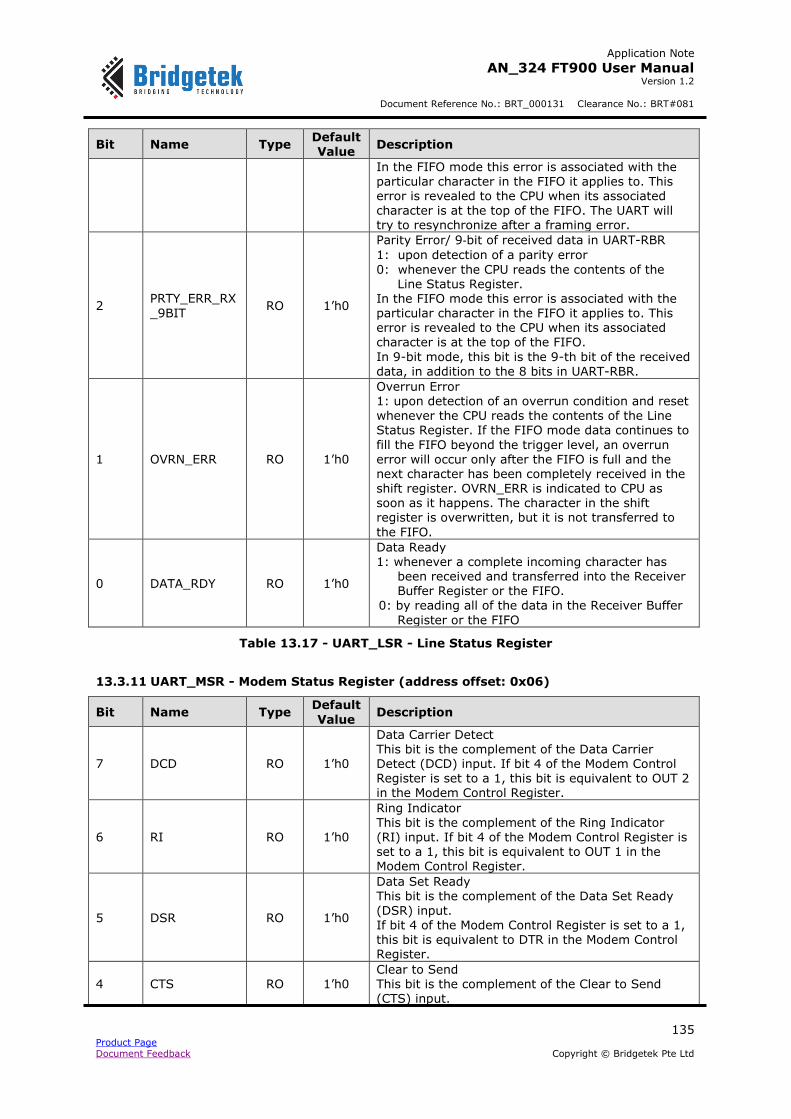
Application Note
AN_324 FT900 User Manual Version 1.2
Document Reference No.: BRT_000131 Clearance No.: BRT#081
135 Product Page Document Feedback Copyright © Bridgetek Pte Ltd
Bit Name Type Default Value
Description
In the FIFO mode this error is associated with the particular character in the FIFO it applies to. This error is revealed to the CPU when its associated character is at the top of the FIFO. The UART will try to resynchronize after a framing error.
2 PRTY_ERR_RX
_9BIT RO 1’h0
Parity Error/ 9‐bit of received data in UART-RBR
1: upon detection of a parity error
0: whenever the CPU reads the contents of the Line Status Register.
In the FIFO mode this error is associated with the particular character in the FIFO it applies to. This error is revealed to the CPU when its associated character is at the top of the FIFO.
In 9-bit mode, this bit is the 9-th bit of the received
data, in addition to the 8 bits in UART-RBR.
1 OVRN_ERR RO 1’h0
Overrun Error 1: upon detection of an overrun condition and reset whenever the CPU reads the contents of the Line Status Register. If the FIFO mode data continues to
fill the FIFO beyond the trigger level, an overrun error will occur only after the FIFO is full and the next character has been completely received in the shift register. OVRN_ERR is indicated to CPU as soon as it happens. The character in the shift register is overwritten, but it is not transferred to
the FIFO.
0 DATA_RDY RO 1’h0
Data Ready 1: whenever a complete incoming character has
been received and transferred into the Receiver Buffer Register or the FIFO.
0: by reading all of the data in the Receiver Buffer
Register or the FIFO
Table 13.17 - UART_LSR - Line Status Register
13.3.11 UART_MSR - Modem Status Register (address offset: 0x06)
Bit Name Type Default
Value Description
7 DCD RO 1’h0
Data Carrier Detect This bit is the complement of the Data Carrier Detect (DCD) input. If bit 4 of the Modem Control Register is set to a 1, this bit is equivalent to OUT 2 in the Modem Control Register.
6 RI RO 1’h0
Ring Indicator This bit is the complement of the Ring Indicator (RI) input. If bit 4 of the Modem Control Register is set to a 1, this bit is equivalent to OUT 1 in the Modem Control Register.
5 DSR RO 1’h0
Data Set Ready This bit is the complement of the Data Set Ready (DSR) input. If bit 4 of the Modem Control Register is set to a 1, this bit is equivalent to DTR in the Modem Control Register.
4 CTS RO 1’h0 Clear to Send This bit is the complement of the Clear to Send (CTS) input.
Application Note
AN_324 FT900 User Manual Version 1.2
Document Reference No.: BRT_000131 Clearance No.: BRT#081
136 Product Page Document Feedback Copyright © Bridgetek Pte Ltd
Bit Name Type Default Value
Description
If bit 4 (LOOPBK_EN) of the Modem control register is set to a 1, this bit is equivalent to RTS in the Modem Control Register.
3 D_DCD RO 1’h0 Delta Data Carrier Detect 1: indicates that the DCD input to the chip has changed state.
2 TERI RO 1’h0 Trailing Edge Ring Indicator 1: Indicates that the RI input to the chip has changed from a low to a high state.
1 D_DSR RO 1’h0
Delta Data Set ready
1: Indicates that the DSR input to the chip has changed state since the last time it was read by the CPU.
0 D_CTS RO 1’h0
Delta Clear To Send
1: Indicates that the CTS input to the chip have changed state since the last time it was read by the
CPU.
Table 13.18 - UART_MSR - Modem Status Register
13.3.12 UART_SPR - SPR Register (address offset: 0x07)
Bit Name Type Default
Value Description
7:0 DATA RW 8’h00
This is the command port for the indexed control register. Writing and reading to indexed control register is addressed by offset written to this register
Table 13.19 - UART_SPR - SPR Register
13.4 650 COMPATIBLE REGISTERS
To access these registers LCR must be set to 0xBF.
13.4.1 UART_EFR - Enhanced Feature Register (address offset: 0x02)
Bit Name Type Default Value
Description
7 CTS_FC RO 1’h0 1: Automatic CTS flow control enable
6 RTS_FC RO 1’h0 1: Automatic RTS flow control enable
5 SPL_CHAR RO 1’h0 1: Special Character Detection mode enable
4 EM RO 1’h0 1: Enhanced mode enable
3:2 IBT_FCM RO 1’h0
In‐band transmit flow control mode
00: Disable in‐band flow control
01: Enable single character in‐band transmit flow
control. Recognizing XON2 as the XON character and XOFF2 as the XOFF character 10: Enable single character in‐band transmit flow
control. Recognizing XON1 as the XON character and XOFF1 as the XOFF character
11: Reserved
Application Note
AN_324 FT900 User Manual Version 1.2
Document Reference No.: BRT_000131 Clearance No.: BRT#081
137 Product Page Document Feedback Copyright © Bridgetek Pte Ltd
1:0 IBR_FCM RO 1’h0
In‐band receive flow control mode
00: Disable in‐band flow control
01: Enable single character in‐band receive flow
control. Recognizing XON2 as the XON character and XOFF2 as the XOFF character 10: Enable single character in‐band receive flow
control. Recognizing XON1 as the XON character and XOFF1 as the XOFF character 11: Reserved
Table 13.20 - UART_EFR - Enhanced Feature Register
13.4.2 UART_XON1 - XON1 Register (address offset: 0x04)
Bit Name Type Default Value
Description
7:0 DATA 8’h00 Value of XON1
Table 13.21 - UART_XON1 - XON1 Register
13.4.3 UART_XON2 - XON2 Register (address offset: 0x05)
Bit Name Type Default Value
Description
7:0 DATA 8’h00 Value of XON2
Table 13.22 - UART_XON2 - XON2 Register
13.4.4 UART_XOFF1 - XOFF1 Register (address offset: 0x06)
Bit Name Type Default
Value Description
7:0 DATA 8’h00 Value of XOFF1
Table 13.23 - UART_XOFF1 - XOFF1 Register
13.4.5 UART_XOFF2 - XOFF2 Register (address offset: 0x07)
Bit Name Type Default
Value Description
7:0 DATA 8’h00 Value of XOFF2
Table 13.24 - UART_XOFF2 - XOFF2 Register
13.5 950 COMPATIBLE REGISTERS
To access these registers ACR[7] must be set to 1.
13.5.1 UART_ASR - Additional Status Register (address offset: 0x01)
Bit Name Type Default Value
Description
7 TX_IDLE RO 1’h0 1: transmitter is idle (transmitter FIFO and shift register are empty)
Application Note
AN_324 FT900 User Manual Version 1.2
Document Reference No.: BRT_000131 Clearance No.: BRT#081
138 Product Page Document Feedback Copyright © Bridgetek Pte Ltd
Bit Name Type Default Value
Description
0: transmitter is transmitting.
6 FIFO_SIZE RO 1’h0 1: FIFO are 16 deep if FCR[0]=1; 0: FIFO are 128 deep if FCR[0]=1
5 FIFO_SEL RO 1’h0 Actual state of FIFOSEL pin
4 SPECIAL_CHAR_DETECT
RO 1’h0
1: special character detect and is stored in UART_RBR ; 0: no special character detect The flag is cleared by reading ASR.
3 DTR RO 1’h0 Complement state of DTR pin
2 RTS RO 1’h0 Complement state of the RTS pin
1 REMOTE_TX_DSBL
RW 1’h0
1: transmitter has sent an XOFF character 0: the remote transmitter is not disabled by in‐ band flow control. This bit may be cleared by software to re‐enable
remote transmitter (XON is sent)
0 TX_DSBL RW 1’h0
1: transmitter disabled (receiver detect XOFF) 0: transmitter is not disabled by in‐ band flow
control. This bit may be cleared by software to re‐enable
transmission if it was disabled by in‐band flow
control.
Table 13.25 - UART_ASR - Additional Status Register
13.5.2 UART_RFL - Receiver FIFO Level Register (address offset: 0x03)
Bit Name Type Defau
lt Value
Description
7:0 DATA RO 8’h00 Number of characters in the receiver FIFO
Table 13.26 - UART_RFL - Receiver FIFO Level Register
Note: Reading from this register requires ACR[7]=1
13.5.3 UART_TFL - Transmitter FIFO Level Register (address offset: 0x04)
Bit Name Type Defau
lt Value
Description
7:0 DATA RO 8’h00 Number of characters in the transmitter FIFO
Table 13.27 - UART_TFL - Transmitter FIFO Level Register
Note: Reading from this register requires that last value written to LCR was not 0xBF and ACR[7]=1
13.5.4 UART_ICR - ICR Register (address offset: 0x05)
Bit Name Type Defau Description

Application Note
AN_324 FT900 User Manual Version 1.2
Document Reference No.: BRT_000131 Clearance No.: BRT#081
139 Product Page Document Feedback Copyright © Bridgetek Pte Ltd
lt Value
7:0 DATA RW 8’h00
Data port to the indexed control register. Writing data to the indexed control register and reading data from the indexed control register is done using this register.
Table 13.28 - UART_ICR - ICR Register
13.6 INDEXED CONTROL REGISTERS
Writing to Indexed Control Registers (ICRs) is addressed by the SPR offset, and data is loaded through the ICR register. Before writing, be sure that the LCR was not loaded with value ‘0xBF’ (it
enables access to 650 compatible registers).To write ICRs please follow these steps:
Figure 13.1 - ICR registers write access
Reading from Indexed Control Registers is addressed by the SPR offset, and data is read through
the ICR register. Before reading be sure that LCR was not loaded with the value ‘0xBF’ (it enables access to 650 compatible registers).To read from ICRs please follow these steps:
SPR ⇐ address
ICR ⇐ value
Yes
Last value written to LCR≠0xBF
No
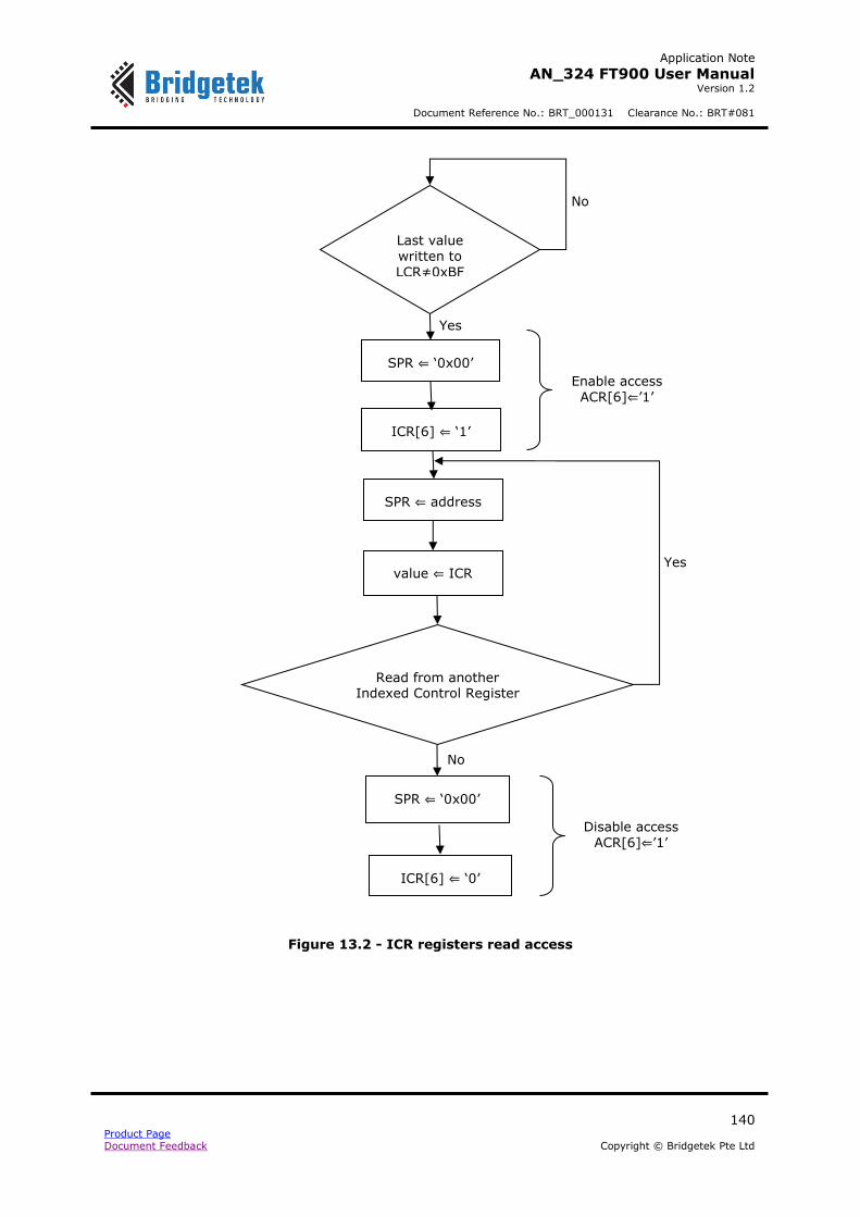
Application Note
AN_324 FT900 User Manual Version 1.2
Document Reference No.: BRT_000131 Clearance No.: BRT#081
140 Product Page Document Feedback Copyright © Bridgetek Pte Ltd
Figure 13.2 - ICR registers read access
No
Disable access ACR[6]⇐’1’
SPR ⇐ ‘0x00’
ICR[6] ⇐ ‘0’
No
Read from another Indexed Control Register
Yes[6] value ⇐ ICR
SPR ⇐ address
Enable access
ACR[6]⇐’1’
Yes
Last value written to LCR≠0xBF
ICR[6] ⇐ ‘1’
SPR ⇐ ‘0x00’

Application Note
AN_324 FT900 User Manual Version 1.2
Document Reference No.: BRT_000131 Clearance No.: BRT#081
141 Product Page Document Feedback Copyright © Bridgetek Pte Ltd
13.6.1 UART_ACR- Additional Control Register (SPR offset: 0x00)
Bit Name Type Default Value
Description
7 ADL_STS_EN RW 1’h0 Additional status enable 1: ASR, TFL and RFL are enabled 0: disabled
6 ICR_RD_EN RW 1’h0 ICR read enable 0: LSR is readable
1: ICR registers are readable
5 950_TLE RW 1’h0
0: Interrupts and flow control trigger levels are described in the FCR register 1: The triggers are set by RTL, TTL, FCL and FCH registers
4:3 DTR RW 1’h0
DTR line configuration When CKS[4] or CKS[5] are set, the transmitter 1x clock or the output of the baud rate generator (Nx
clock) are asserted on the DTR pin, otherwise the pin is defined as follows: 00: DTR pin is compatible with 450, 550, 650 and
750 (i.e. normal). 01: DTR pin is used for out‐of‐band flow control. It
will be forced high, when the receiver FIFO level reaches the upper flow control trigger (FCH). It will be forced low when the receiver FIFO level falls below the lower flow control trigger (FCL). 10: DTR is configured to drive the active low enable
pin of an external RS485 buffer. The pin will be forced low whenever the transmitter is not empty (LSR[6]=0), otherwise the pin is high. 11: DTR is configured to drive the active high enable pin of the external RS485 buffer. The pin will be forced high whenever the transmitter is not empty (LSR[6]=0), otherwise the pin is low.
2 DSR RW 1’h0 1: enables automatic out‐of‐band flow control using
the DSR pin
1 TX RW 1’h0
Transmitter disable. 0: Transmitter is enabled. 1: Transmitter is disabled. Data in THR are not transmitted. In‐band flow control characters may
still be transmitted.
0 RX RW 1’h0
Receiver disable. 0: Receiver is enabled and data are stored in UART_RBR. 1: Receiver is disabled. The receiver continues to
operate as normal to maintain frame synchronization but received data are not stored. In‐band control characters continue to be detected
and acted upon. Special characters will not be detected.
Table 13.29 - UART_ACR- Additional Control Register
13.6.2 UART_CPR - Clock Prescaler Register (SPR offset: 0x01)
Bit Name Type Default Value
Description
7:3 PSCL RW 5’h00 clock prescaler
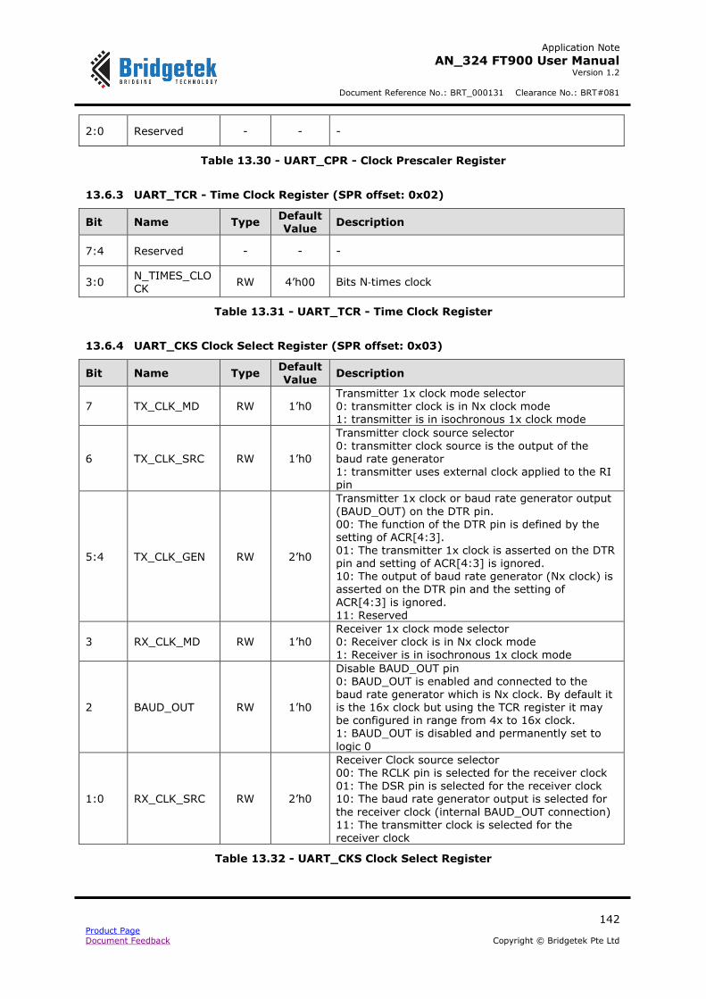
Application Note
AN_324 FT900 User Manual Version 1.2
Document Reference No.: BRT_000131 Clearance No.: BRT#081
142 Product Page Document Feedback Copyright © Bridgetek Pte Ltd
2:0 Reserved - - -
Table 13.30 - UART_CPR - Clock Prescaler Register
13.6.3 UART_TCR - Time Clock Register (SPR offset: 0x02)
Bit Name Type Default Value
Description
7:4 Reserved - - -
3:0 N_TIMES_CLOCK
RW 4’h00 Bits N‐times clock
Table 13.31 - UART_TCR - Time Clock Register
13.6.4 UART_CKS Clock Select Register (SPR offset: 0x03)
Bit Name Type Default
Value Description
7 TX_CLK_MD RW 1’h0 Transmitter 1x clock mode selector 0: transmitter clock is in Nx clock mode 1: transmitter is in isochronous 1x clock mode
6 TX_CLK_SRC RW 1’h0
Transmitter clock source selector 0: transmitter clock source is the output of the baud rate generator 1: transmitter uses external clock applied to the RI pin
5:4 TX_CLK_GEN RW 2’h0
Transmitter 1x clock or baud rate generator output
(BAUD_OUT) on the DTR pin. 00: The function of the DTR pin is defined by the setting of ACR[4:3]. 01: The transmitter 1x clock is asserted on the DTR
pin and setting of ACR[4:3] is ignored. 10: The output of baud rate generator (Nx clock) is asserted on the DTR pin and the setting of
ACR[4:3] is ignored. 11: Reserved
3 RX_CLK_MD RW 1’h0 Receiver 1x clock mode selector 0: Receiver clock is in Nx clock mode 1: Receiver is in isochronous 1x clock mode
2 BAUD_OUT RW 1’h0
Disable BAUD_OUT pin 0: BAUD_OUT is enabled and connected to the baud rate generator which is Nx clock. By default it is the 16x clock but using the TCR register it may be configured in range from 4x to 16x clock. 1: BAUD_OUT is disabled and permanently set to
logic 0
1:0 RX_CLK_SRC RW 2’h0
Receiver Clock source selector 00: The RCLK pin is selected for the receiver clock
01: The DSR pin is selected for the receiver clock 10: The baud rate generator output is selected for
the receiver clock (internal BAUD_OUT connection) 11: The transmitter clock is selected for the receiver clock
Table 13.32 - UART_CKS Clock Select Register
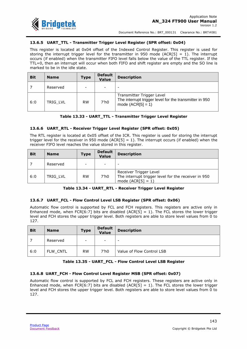
Application Note
AN_324 FT900 User Manual Version 1.2
Document Reference No.: BRT_000131 Clearance No.: BRT#081
143 Product Page Document Feedback Copyright © Bridgetek Pte Ltd
13.6.5 UART_TTL - Transmitter Trigger Level Register (SPR offset: 0x04)
This register is located at 0x04 offset of the Indexed Control Register. This register is used for storing the interrupt trigger level for the transmitter in 950 mode (ACR[5] = 1). The interrupt occurs (if enabled) when the transmitter FIFO level falls below the value of the TTL register. If the TTL=0, then an interrupt will occur when both FIFO and shift register are empty and the SO line is
marked to be in the idle state.
Bit Name Type Default Value
Description
7 Reserved - - -
6:0 TRIG_LVL RW 7’h0
Transmitter Trigger Level
The interrupt trigger level for the transmitter in 950 mode (ACR[5] = 1)
Table 13.33 - UART_TTL - Transmitter Trigger Level Register
13.6.6 UART_RTL - Receiver Trigger Level Register (SPR offset: 0x05)
The RTL register is located at 0x05 offset of the ICR. This register is used for storing the interrupt trigger level for the receiver in 950 mode (ACR[5] = 1). The interrupt occurs (if enabled) when the receiver FIFO level reaches the value stored in this register.
Bit Name Type Default Value
Description
7 Reserved - - -
6:0 TRIG_LVL RW 7’h0 Receiver Trigger Level The interrupt trigger level for the receiver in 950 mode (ACR[5] = 1)
Table 13.34 - UART_RTL - Receiver Trigger Level Register
13.6.7 UART_FCL - Flow Control Level LSB Register (SPR offset: 0x06)
Automatic flow control is supported by FCL and FCH registers. This registers are active only in
Enhanced mode, when FCR[6:7] bits are disabled (ACR[5] = 1). The FCL stores the lower trigger level and FCH stores the upper trigger level. Both registers are able to store level values from 0 to 127.
Bit Name Type Default Value
Description
7 Reserved - - -
6:0 FLW_CNTL RW 7’h0 Value of Flow Control LSB
Table 13.35 - UART_FCL - Flow Control Level LSB Register
13.6.8 UART_FCH - Flow Control Level Register MSB (SPR offset: 0x07)
Automatic flow control is supported by FCL and FCH registers. These registers are active only in Enhanced mode, when FCR[6:7] bits are disabled (ACR[5] = 1). The FCL stores the lower trigger level and FCH stores the upper trigger level. Both registers are able to store level values from 0 to 127.
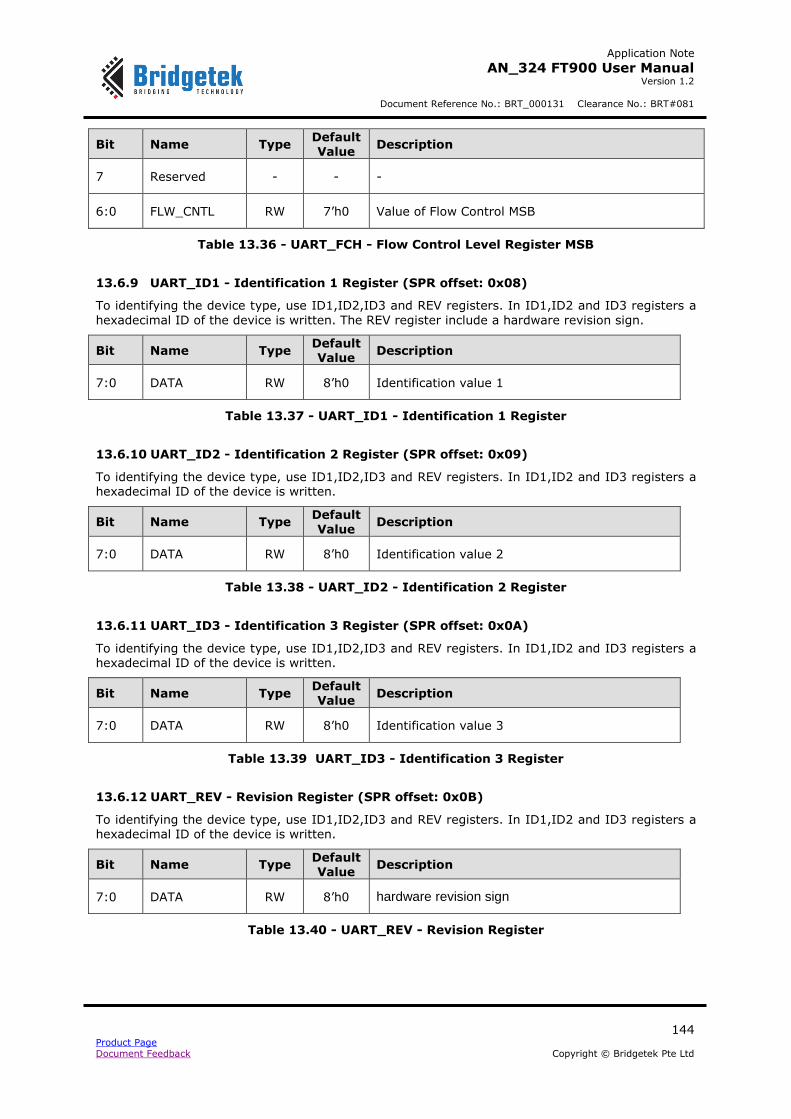
Application Note
AN_324 FT900 User Manual Version 1.2
Document Reference No.: BRT_000131 Clearance No.: BRT#081
144 Product Page Document Feedback Copyright © Bridgetek Pte Ltd
Bit Name Type Default Value
Description
7 Reserved - - -
6:0 FLW_CNTL RW 7’h0 Value of Flow Control MSB
Table 13.36 - UART_FCH - Flow Control Level Register MSB
13.6.9 UART_ID1 - Identification 1 Register (SPR offset: 0x08)
To identifying the device type, use ID1,ID2,ID3 and REV registers. In ID1,ID2 and ID3 registers a
hexadecimal ID of the device is written. The REV register include a hardware revision sign.
Bit Name Type Default Value
Description
7:0 DATA RW 8’h0 Identification value 1
Table 13.37 - UART_ID1 - Identification 1 Register
13.6.10 UART_ID2 - Identification 2 Register (SPR offset: 0x09)
To identifying the device type, use ID1,ID2,ID3 and REV registers. In ID1,ID2 and ID3 registers a hexadecimal ID of the device is written.
Bit Name Type Default Value
Description
7:0 DATA RW 8’h0 Identification value 2
Table 13.38 - UART_ID2 - Identification 2 Register
13.6.11 UART_ID3 - Identification 3 Register (SPR offset: 0x0A)
To identifying the device type, use ID1,ID2,ID3 and REV registers. In ID1,ID2 and ID3 registers a hexadecimal ID of the device is written.
Bit Name Type Default Value
Description
7:0 DATA RW 8’h0 Identification value 3
Table 13.39 UART_ID3 - Identification 3 Register
13.6.12 UART_REV - Revision Register (SPR offset: 0x0B)
To identifying the device type, use ID1,ID2,ID3 and REV registers. In ID1,ID2 and ID3 registers a hexadecimal ID of the device is written.
Bit Name Type Default Value
Description
7:0 DATA RW 8’h0 hardware revision sign
Table 13.40 - UART_REV - Revision Register
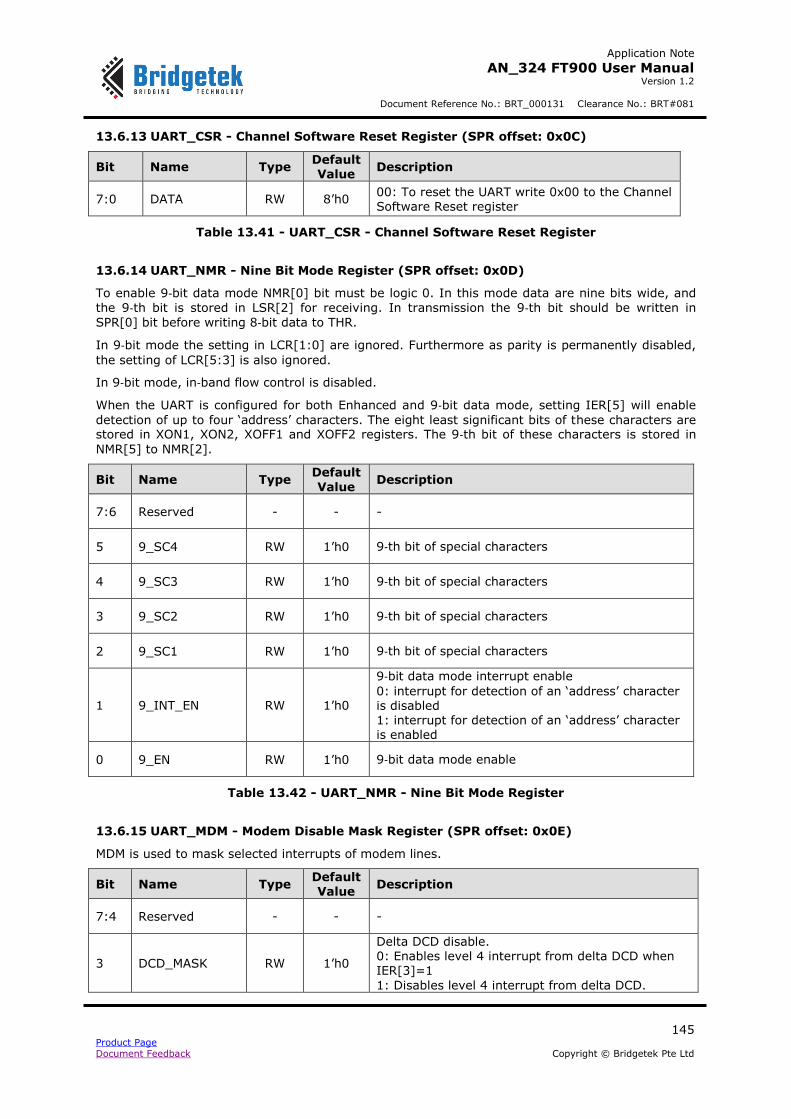
Application Note
AN_324 FT900 User Manual Version 1.2
Document Reference No.: BRT_000131 Clearance No.: BRT#081
145 Product Page Document Feedback Copyright © Bridgetek Pte Ltd
13.6.13 UART_CSR - Channel Software Reset Register (SPR offset: 0x0C)
Bit Name Type Default Value
Description
7:0 DATA RW 8’h0 00: To reset the UART write 0x00 to the Channel Software Reset register
Table 13.41 - UART_CSR - Channel Software Reset Register
13.6.14 UART_NMR - Nine Bit Mode Register (SPR offset: 0x0D)
To enable 9‐bit data mode NMR[0] bit must be logic 0. In this mode data are nine bits wide, and
the 9‐th bit is stored in LSR[2] for receiving. In transmission the 9‐th bit should be written in
SPR[0] bit before writing 8‐bit data to THR.
In 9‐bit mode the setting in LCR[1:0] are ignored. Furthermore as parity is permanently disabled,
the setting of LCR[5:3] is also ignored.
In 9‐bit mode, in‐band flow control is disabled.
When the UART is configured for both Enhanced and 9‐bit data mode, setting IER[5] will enable
detection of up to four ‘address’ characters. The eight least significant bits of these characters are stored in XON1, XON2, XOFF1 and XOFF2 registers. The 9‐th bit of these characters is stored in
NMR[5] to NMR[2].
Bit Name Type Default
Value Description
7:6 Reserved - - -
5 9_SC4 RW 1’h0 9‐th bit of special characters
4 9_SC3 RW 1’h0 9‐th bit of special characters
3 9_SC2 RW 1’h0 9‐th bit of special characters
2 9_SC1 RW 1’h0 9‐th bit of special characters
1 9_INT_EN RW 1’h0
9‐bit data mode interrupt enable
0: interrupt for detection of an ‘address’ character is disabled 1: interrupt for detection of an ‘address’ character is enabled
0 9_EN RW 1’h0 9‐bit data mode enable
Table 13.42 - UART_NMR - Nine Bit Mode Register
13.6.15 UART_MDM - Modem Disable Mask Register (SPR offset: 0x0E)
MDM is used to mask selected interrupts of modem lines.
Bit Name Type Default Value
Description
7:4 Reserved - - -
3 DCD_MASK RW 1’h0
Delta DCD disable. 0: Enables level 4 interrupt from delta DCD when IER[3]=1
1: Disables level 4 interrupt from delta DCD.
Application Note
AN_324 FT900 User Manual Version 1.2
Document Reference No.: BRT_000131 Clearance No.: BRT#081
146 Product Page Document Feedback Copyright © Bridgetek Pte Ltd
Bit Name Type Default Value
Description
2 RI_MASK RW 1’h0
Trailing edge RI disable. 0: Enables level 4 interrupt from trailing edge RI when IER[3]=1 1: Disables level 4 interrupt from trailing edge RI.
1 DSR_MASK RW 1’h0
Delta DSR disable. 0: Enables level 4 interrupt from delta DSR when
IER[3]=1 1: Disables level 4 interrupt from delta DSR.
0 CTS_MASK RW 1’h0
Delta CTS disable. 0: Enables level 4 interrupt from delta CTS when IER[3]=1 1: Disables level 4 interrupt from delta CTS.
Table 13.43 - UART_MDM - Modem Disable Mask Register
13.6.16 UART_RFC - Readable FCR Register (SPR offset: 0x0F)
Bit Name Type Default Value
Description
7:0 FCR RO 8’h00 read the state of FCR register
Table 13.44 - UART_RFC - Readable FCR Register
13.6.17 UART_GDS - Good Data Status Register (SPR offset: 0x10)
Good data status is set when the following conditions are true:
ISR reads level 0 (no interrupt), level 2 or 2a (receiver data) or level 3 (THR empty) interrupt.
LSR[7] is clear. LSR[1] is clear.
Bit Name Type Default Value
Description
7:0 DATA RO 8’h00 contains ‘good data status’ bit on least significant position.
Table 13.45 - UART_GDS - Good Data Status Register
13.6.18 UART_RSRV_1 - Reserved 1 Register (SPR offset: 0x11)
Bit Name Type Default Value
Description
7:0 Reserved - - -
Table 13.46 - UART_RSRV_1 - Reserved 1 Register
13.6.19 UART_PIDX - Port Index Register (SPR offset: 0x12)
Bit Name Type Default Value
Description
7:0 DATA RO 8’h00 The value of UART index is 0.
Table 13.47 - UART_PIDX - Port Index Register
Application Note
AN_324 FT900 User Manual Version 1.2
Document Reference No.: BRT_000131 Clearance No.: BRT#081
147 Product Page Document Feedback Copyright © Bridgetek Pte Ltd
13.6.20 UART_CKA - Clock Alteration Register (SPR offset: 0x13)
Bit Name Type Default Value
Description
7:5 Reserved - - -
4 CLK_TXRDY RW 1’h0 Output system clock on TxRdy pin
3 CLK_SEL RW 1’h0 Use CLKSEL pin for system clock
2 INV_DTR RW 1’h0 Invert DTR signal
1 INV_TX_CLK RW 1’h0 Invert internal Tx clock
0 INV_RX_CLK RW 1’h0 Invert internal Rx clock
Table 13.48 - UART_CKA - Clock Alteration Register
Application Note
AN_324 FT900 User Manual Version 1.2
Document Reference No.: BRT_000131 Clearance No.: BRT#081
148 Product Page Document Feedback Copyright © Bridgetek Pte Ltd
14 Timers and Watchdog
FT900 consists of a 32-bit watchdog timer and four 16-bit users’ timers.
The watchdog timer is clocked off the main clock. The watchdog can be initialized with a 5-bit register. The value of this register points to a bit of the 32-bit counter which will be set. A timer decrements and signals an interrupt when it rolls over. Once started and initialized the watchdog cannot be stopped. It can be cleared by writing into a register.
Four user timers can be clocked off the main clock or a common 16-bit prescaler, which can be
selected for each timer individually. These timers can be started, stopped and cleared/initialized. Current values of all four user timers can be read from registers (one at a time - common register, multiplexed access). All timers count up or down and signal an interrupt when rolling over. Each of the timers can be configured to be one-shot or in continuous mode. They are initialized from a common register and only one at a time (multiplexed access).
The Prescaler block is a 16-bit timer/counter. It can be cleared/initialized by writing into a register
the same as with other timers, however if one of the user timers has already started using the
prescaler it cannot be cleared and the command is ignored. The Prescaler automatically stops after clear. It also starts automatically when any of the user timers using it starts.
All timers (4 user timers, prescaler and watchdog) instantiate the same block. Setting clear input high, depending on the direction input value, initializes the timer with a final value if counting up or 0 when counting down. Start input triggers a timer which increments/decrements synchronously with an enable signal. Setting mode input high causes a timer to stop when it rolls over.
Normal operation:
User timers Prescaler Watchdog
Select the timer to initialize by writing into the TIMER_SELECT register. Write initial/final value into
TIMER_WRITE_LS and TIMER_WRITE_MS registers.
Write initial value into TIMER_PRESC_LS and TIMER_PRESC_MS
registers.
Write initial value into TIMER_WDG register to initialize one of the 32 bits of the timer.
Write into direction bit in TIMER_CONTROL_3 register to select
up/down counting.
N/A N/A
Write into mode bit in TIMER_CONTROL_3 register to select mode.
N/A N/A
Write into clear_x bits in
TIMER_CONTROL_4 register to initialize the timer.
Write into clear_presc bit in
TIMER_CONTROL_4 register to initialize the prescaler (if possible)
Write into clear_wdg bit in
TIMER_CONTROL_2 register to clear watchdog.
Write into start_x bits in TIMER_CONTROL_1 register to start the timer.
Write into prescaler_en bit in
TIMER_CONTROL_2 register to enable prescaler and it will automatically start when the timer/timers using it starts.
Write into start_wdg bit in TIMER_CONTROL_2 register to start
watchdog.
Select timer you want to read from by writing into timer_read_sel bit in TIMER_SELECT register. Current value can be read from TIMER_READ_LS and TIMER_READ_MS registers.
N/A N/A
Write into stop_x bit in TIMER_CONTROL_1 register to stop the timer.
N/A N/A

Application Note
AN_324 FT900 User Manual Version 1.2
Document Reference No.: BRT_000131 Clearance No.: BRT#081
149 Product Page Document Feedback Copyright © Bridgetek Pte Ltd
Table 14.1 - Timers/Watchdog Operation
14.1 Register Summary
Listed below are the registers with their offset from the base address (0x10340). All registers can only be accessed via Byte (8-bit) mode.
Offset Register Default value
References
0x00 TIMER_CONTROL_0 - Timers Control Register 0 0x00 Section 14.2.1
0x01 TIMER_CONTROL_1 - Timers Control Register 1 0x00 Section 14.2.2
0x02 TIMER_CONTROL_2 - Timers Control Register 2 0x00 Section 14.2.3
0x03 TIMER_CONTROL_3 - Timers Control Register 3 0x00 Section 14.2.4
0x04 TIMER_CONTROL_4 - Timers Control Register 4 0x00 Section 14.2.5
0x05 TIMER_INT - Timers Interrupt Register 0x00 Section 14.2.6
0x06 TIMER_SELECT - Timers A..D Select Register 0x00 Section 14.2.7
0x07 TIMER_WDG - Watchdog Start Value 0x00 Section 14.2.8
0x08 TIMER_WRITE_LS - Timer A..D Start Value 7:0 0x00 Section 14.2.9
0x09 TIMER_WRITE_MS - Timer A..D Start Value 15:8 0x00 Section 14.2.10
0x0A TIMER_PRESC_LS - Prescaler Start Value 7:0 0x00 Section 14.2.11
0x0B TIMER_PRESC_MS - Prescaler Start Value 15:8 0x00 Section 14.2.12
0x0C TIMER_READ_LS - Timer A..D Current Value 7:0 0x00 Section 14.2.13
0x0D
TIMER_READ_MS - Timer A..D Current Value 15:8
0x00
Section 14.2.14
Table 14.2 - Overview of Timers/Watchdog Registers
14.2 Register Details
14.2.1 TIMER_CONTROL_0 - Timers Control Register 0 (address offset: 0x00)
Bit Name Type Default
Value Description
1 block_en RW 1’b0 1: To enable the timer module
0 soft_reset RWAC 1’b0 1: Write 1 to trigger the reset
Table 14.3 - TIMER_CONTROL_0 - Timers Control Register 0
14.2.2 TIMER_CONTROL_1 - Timers Control Register 1 (address offset: 0x01)
Bit Name Type Default Value
Description
7 stop_d RWAC 1’b0 1: To trigger stopping timer D
6 stop_c RWAC 1’b0 1: To trigger stopping timer C
5 stop_b RWAC 1’b0 1: To trigger stopping timer B

Application Note
AN_324 FT900 User Manual Version 1.2
Document Reference No.: BRT_000131 Clearance No.: BRT#081
150 Product Page Document Feedback Copyright © Bridgetek Pte Ltd
4 stop_a RWAC 1’b0 1: To trigger stopping timer A
3 start_d RWAC 1’b0 1: To trigger starting timer D
2 start_c RWAC 1’b0 1: To trigger starting timer C
1 start_b RWAC 1’b0 1: To trigger starting timer B
0 start_a RWAC 1’b0 1: To trigger starting timer A
Table 14.4 - TIMER_CONTROL_1 - Timers Control Register 1
14.2.3 TIMER_CONTROL_2 - Timers Control Register 2 (address offset: 0x02)
Bit Name Type Default Value
Description
7:4 prescaler_en RW 4’h0 Enable prescaler bits for timers D/C/B/A respectively
3 wdg_int_ien RW 1’b0 1: enable watch dog interrupt
2 wdg_int RW1C 1’b0 1: watch-dog interrupt pending
1 clear_wdg RWAC 1’b0 1: To trigger clearing watch dog timer
0 start_wdg RWAC 1’b0 1: To trigger starting watch dog timer
Table 14.5 - TIMER_CONTROL_2 - Timers Control Register 2
14.2.4 TIMER_CONTROL_3 - Timers Control Register 3 (address offset: 0x03)
Bit Name Type Default Value
Description
7:4 direction RW 4’h0 Counter direction bits for timers D/C/B/A respectively
1: Up 0: Down
3:0 mode RW 4’h0 Continuous/1-shot mode bits for timers D/C/B/A respectively 1: 1-shot 0: Continuous
Table 14.6 - TIMER_CONTROL_3 - Timers Control Register 3
14.2.5 TIMER_CONTROL_4 - Timers Control Register 4 (address offset: 0x04)
Bit Name Type Default Value
Description
4 presc_clear RWAC 1’b0 1: To trigger clearing prescaler
3 clear_d RWAC 1’b0 1: To trigger clearing timer D
2 clear_c RWAC 1’b0 1: To trigger clearing timer C
1 clear_b RWAC 1’b0 1: To trigger clearing timer B
0 clear_a RWAC 1’b0 1: To trigger clearing timer A
Table 14.7 - TIMER_CONTROL_4 - Timers Control Register 4
14.2.6 TIMER_INT - Timers Interrupt Register (address offset: 0x05)
Bit Name Type Default
Value Description
7 timer_int_d_en RW 1’b0 1: Enable timer D interrupt
6 timer_int_d RW1C 1’b0 1: Timer D interrupt pending
5 timer_int_c_en RW 1’b0 1: Enable timer C interrupt
4 timer_int_c RW1C 1’b0 1: Timer C interrupt pending
3 timer_int_b_en RW 1’b0 1: Enable timer B interrupt
2 timer_int_b RW1C 1’b0 1: Timer B interrupt pending
1 timer_int_a_en RW 1’b0 1: Enable timer A interrupt

Application Note
AN_324 FT900 User Manual Version 1.2
Document Reference No.: BRT_000131 Clearance No.: BRT#081
151 Product Page Document Feedback Copyright © Bridgetek Pte Ltd
Bit Name Type Default Value
Description
0 timer_int_a RW1C 1’b0 1: Timer A interrupt pending
Table 14.8 - TIMER_INT - Timers Interrupt Register
14.2.7 TIMER_SELECT - Timers A..D Select Register (address offset: 0x06)
Bit Name Type Default Value
Description
3:2 timer_read_sel RW 2’h0 Select one of Timers A/B/C/D to read (value 0/1/2/3)
1:0 timer_write_sel RW 2’h0 Select one of Timers A/B/C/D to write (value 0/1/2/3)
Table 14.9 - TIMER_SELECT - Timers A..D Select Register
14.2.8 TIMER_WDG - Watchdog Start Value (address offset: 0x07)
Bit Name Type Default Value
Description
4:0 timer_wdg_write
RW 5’h00 Setting watchdog value
5’h00 32’h0000_0001
5’h01 32’h0000_0002
… …
5’h1E 32’h4000_0000
5’h1F 32’h8000_0000
Table 14.10 - TIMER_WDG - Watchdog Start Value
14.2.9 TIMER_WRITE_LS - Timer A..D Start Value 7:0 (address offset: 0x08)
Bit Name Type Default Value
Description
7:0 timer_write_7_0 RW 8’h00 Write low byte of the timer start value
Table 14.11 - TIMER_WRITE_LS - Timer A..D Start Value 7:0
14.2.10 TIMER_WRITE_MS - Timer A..D Start Value 15:8 (address offset: 0x09)
Bit Name Type Default
Value Description
7:0 timer_write_15_8
RW 8’h00 Write high byte of the timer start value
Table 14.12 - TIMER_WRITE_MS - Timer A..D Start Value 15:8
14.2.11 TIMER_PRESC_LS - Prescaler Start Value 7:0 (address offset: 0x0A)
Bit Name Type Default Value
Description
7:0 timer_presc_7_0
RW 8’h00 Write low byte of the timer prescaler start value
Table 14.13 - TIMER_PRESC_LS - Prescaler Start Value 7:0
14.2.12 TIMER_PRESC_MS - Prescaler Start Value 15:8 (address offset: 0x0B)
Bit Name Type Default Value
Description
Application Note
AN_324 FT900 User Manual Version 1.2
Document Reference No.: BRT_000131 Clearance No.: BRT#081
152 Product Page Document Feedback Copyright © Bridgetek Pte Ltd
7:0 timer_presc_15_8
RW 8’h00 Write high byte of the timer prescaler start value
Table 14.14 - TIMER_PRESC_MS - Prescaler Start Value 15:8
14.2.13 TIMER_READ_LS - Timer A..D Current Value 7:0 (address offset: 0x0C)
Bit Name Type Default Value
Description
7:0 timer_read_7_0 RO 8’h00 Read low byte of the timer start value
Table 14.15 - TIMER_READ_LS - Timer A..D Current Value 7:0
14.2.14 TIMER_READ_MS - Timer A..D Current Value 15:8 (address offset: 0x0D)
Bit Name Type Default Value
Description
7:0 timer_read_15_8
RO 8’h00 Read high byte of the timer start value
Table 14.16 - TIMER_READ_MS - Timer A..D Current Value 15:8
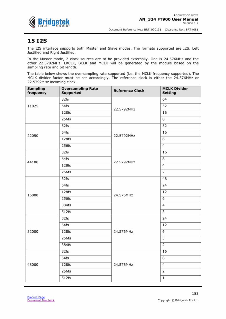
Application Note
AN_324 FT900 User Manual Version 1.2
Document Reference No.: BRT_000131 Clearance No.: BRT#081
153 Product Page Document Feedback Copyright © Bridgetek Pte Ltd
15 I2S
The I2S interface supports both Master and Slave modes. The formats supported are I2S, Left Justified and Right Justified.
In the Master mode, 2 clock sources are to be provided externally. One is 24.576MHz and the other 22.5792MHz. LRCLK, BCLK and MCLK will be generated by the module based on the sampling rate and bit length.
The table below shows the oversampling rate supported (i.e. the MCLK frequency supported). The MCLK divider factor must be set accordingly. The reference clock is either the 24.576MHz or 22.5792MHz incoming clock.
Sampling frequency
Oversampling Rate Supported
Reference Clock MCLK Divider Setting
11025
32fs
22.5792MHz
64
64fs 32
128fs 16
256fs 8
22050
32fs
22.5792MHz
32
64fs 16
128fs 8
256fs 4
44100
32fs
22.5792MHz
16
64fs 8
128fs 4
256fs 2
16000
32fs
24.576MHz
48
64fs 24
128fs 12
256fs 6
384fs 4
512fs 3
32000
32fs
24.576MHz
24
64fs 12
128fs 6
256fs 3
384fs 2
48000
32fs
24.576MHz
16
64fs 8
128fs 4
256fs 2
512fs 1
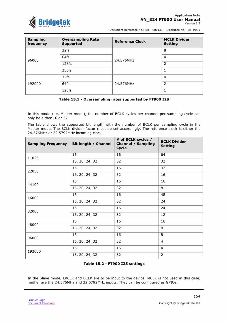
Application Note
AN_324 FT900 User Manual Version 1.2
Document Reference No.: BRT_000131 Clearance No.: BRT#081
154 Product Page Document Feedback Copyright © Bridgetek Pte Ltd
Sampling frequency
Oversampling Rate Supported
Reference Clock MCLK Divider Setting
96000
32fs
24.576MHz
8
64fs 4
128fs 2
256fs 1
192000
32fs
24.576MHz
4
64fs 2
128fs 1
Table 15.1 - Oversampling rates supported by FT900 I2S
In this mode (i.e. Master mode), the number of BCLK cycles per channel per sampling cycle can
only be either 16 or 32.
The table shows the supported bit length with the number of BCLK per sampling cycle in the Master mode. The BCLK divider factor must be set accordingly. The reference clock is either the 24.576MHz or 22.5792MHz incoming clock.
Sampling Frequency Bit length / Channel # of BCLK cycles / Channel / Sampling
Cycle
BCLK Divider Setting
11025 16 16 64
16, 20, 24, 32 32 32
22050 16 16 32
16, 20, 24, 32 32 16
44100 16 16 16
16, 20, 24, 32 32 8
16000 16 16 48
16, 20, 24, 32 32 24
32000 16 16 24
16, 20, 24, 32 32 12
48000 16 16 16
16, 20, 24, 32 32 8
96000 16 16 8
16, 20, 24, 32 32 4
192000 16 16 4
16, 20, 24, 32 32 2
Table 15.2 - FT900 I2S settings
In the Slave mode, LRCLK and BCLK are to be input to the device. MCLK is not used in this case; neither are the 24.576MHz and 22.5792MHz inputs. They can be configured as GPIOs.

Application Note
AN_324 FT900 User Manual Version 1.2
Document Reference No.: BRT_000131 Clearance No.: BRT#081
155 Product Page Document Feedback Copyright © Bridgetek Pte Ltd
In the Slave mode, the incoming/outgoing data can be 16, 20, 24 or 32 bits per channel. And the incoming number of BCLK cycles per sampling period can be 16, 20, 24 or 32. The data length can be X-bit per channel whereas the number of BCLK cycles per sampling period can be any setting mentioned that is larger or equal to X-bit. For example, 16-bit data length per channel can be supported with any of 16, 20, 24 or 32 BCLK cycles per sampling period setting. However, the
maximum frequency of BCLK is 12.288MHz regardless of the sampling frequency and bit length.
15.1 Register Summary
Listed below are the registers with their offset from the base address (0x10350). All registers can only be accessed via Word (16-bit) mode.
Offset Register Default value
References
0x00 I2SCR - Configuration Register 1 0x00 Section 15.2.1
0x02 I2SCR2 - Configuration Register 2 0x00 Section 15.2.2
0x04 I2SIRQEN - Interrupt Enable Register 0x00 Section 15.2.3
0x06 I2SIRQPEND - Interrupt Pending Register 0x00 Section 15.2.4
0x08 I2SRWDATA - Transmit / Receive Data Register 0x00 Section 15.2.5
0x0C I2SRXCOUNT - RX Count Register 0x00 Section 15.2.6
0x0E I2STXCOUNT - TX Count Register 0x00 Section 15.2.7
Table 15.3 - Overview of I2S Registers
15.2 Register Details
15.2.1 I2SCR - Configuration Register 1 (address offset: 0x00)
Bit Name Type Default Value
Description
15 Soft Reset RW 1’b0 1: To turn on the soft reset. 0: To turn off the soft reset.
14:12 Padding RW 3’h0 0: No padding required; (bit length = number of bclk cycles) 1: 4 extra 0 bits are added.
2: 8 extra 0 bits are added. 3: 12 extra 0 bits are added. 4: 16 extra 0 bits are added. Others: Reserved
11:10 Format RW 2’h0 0: I2S Format.
1: Left Justified Format.
2: Right Justified Format. Others: Reserved
9:8 Bit Length RW 2’h0 0: 16-bit Format. 1: 20-bit Format. 2: 24-bit Format.
3: 32-bit Format.
7 IsMaster64 RW 1’b0 This is valid for I2S Master mode only. 1: 32 BCLK cycles per channel;.

Application Note
AN_324 FT900 User Manual Version 1.2
Document Reference No.: BRT_000131 Clearance No.: BRT#081
156 Product Page Document Feedback Copyright © Bridgetek Pte Ltd
0: 16 BCLK cycles per channel.
6 MasterMode RW 1’b0 1: Set I2S to the Master Mode.
5 IsMaster22 RW 1’b0 This is valid for I2S Master mode only. 1: Use 22.5792MHz input as the reference clock. 0: Use 24.576MHz input as the reference clock.
4 BCLK Polarity RW 1’b0 1: Invert the polarity of BCLK.
3 LRCLK Out Polarity
RW 1’b0 1: Invert the polarity of LRCLK for reception.
2 LRCLK In
Polarity
RW 1’b0 1: Inver the polarity of LRCLK for
transmission.
1 RX Enable RW 1’b0 1: Enable the receive channel.
0 TX Enable RW 1’b0 1: Enable the transmit channel.
Table 15.4 - I2SCR - Configuration Register 1
15.2.2 I2SCR2 - Configuration Register 2 (address offset: 0x02)
Bit Name Type Default Value
Description
15:12 Reserved - - -
11:8 MCLK Divider RW 4’h0 This is valid for I2S Master mode only. 0: No division (MCLK = reference clock). 1: Divide by 2. 2: Divide by 3. 3: Divide by 4. 4: Divide by 6.
5: Divide by 8. 6: Divide by 12. 7: Divide by 16. 8: Divide by 24. 9: Divide by 32. A: Divide by 48.
B: Divide by 64. Others: Reserved
7:4 Reserved - - -
3:0 BCLK Divider RW 4’h0 This is valid for I2S Master mode only. 0: No division (MCLK = reference clock).
1: Divide by 2. 2: Divide by 3. 3: Divide by 4. 4: Divide by 6. 5: Divide by 8. 6: Divide by 12.
7: Divide by 16. 8: Divide by 24. 9: Divide by 32. A: Divide by 48. B: Divide by 64. Others: Reserved
Table 15.5 - I2SCR2 - Configuration Register 2
15.2.3 I2SIRQEN - Interrupt Enable Register (address offset: 0x04)
Bit Name Type Default Value
Description
15:13 Reserved - - -
12 RX FIFO Ov RW 1’b0 1: Enable Receive FIFO Overflow Interrupt.

Application Note
AN_324 FT900 User Manual Version 1.2
Document Reference No.: BRT_000131 Clearance No.: BRT#081
157 Product Page Document Feedback Copyright © Bridgetek Pte Ltd
Bit Name Type Default Value
Description
11 RX FIFO Full RW 1’b0 1: Enable Receive FIFO Full Interrupt.
10 RX FIFO Half RW 1’b0 1: Enable Receive FIFO Half Full Interrupt.
9 RX FIFO Empty
RW 1’b0 1: Enable Receive FIFO Empty Interrupt.
8 RX FIFO Under RW 1’b0 1: Enable Receive FIFO Underflow Interrupt.
7:5 Reserved - - -
4 TX FIFO Ov RW 1’b0 1: Enable Transmit FIFO Overflow Interrupt.
3 TX FIFO Full RW 1’b0 1: Enable Transmit FIFO Full Interrupt.
2 TX FIFO Half RW 1’b0 1: Enable Transmit FIFO Half Full Interrupt.
1 TX FIFO Empty
RW 1’b0 1: Enable Transmit FIFO Empty Interrupt.
0 TX FIFO Under RW 1’b0 1: Enable Transmit FIFO Underflow Interrupt.
Table 15.6 - I2SIRQEN - Interrupt Enable Register
15.2.4 I2SIRQPEND - Interrupt Pending Register (address offset: 0x06)
Bit Name Type Default
Value Description
15:13 Reserved - - -
12 RX FIFO Ov RW1C 1’b0 1: Receive FIFO Overflow Interrupt Pending. Write 1 to clear.
11 RX FIFO Full RW1C 1’b0 1: Receive FIFO Full Interrupt Pending. Write 1 to clear.
10 RX FIFO Half RW1C 1’b0 1: Receive FIFO Half Full Interrupt Pending. Write 1 to clear.
9 RX FIFO Empty
RW1C 1’b0 1: Receive FIFO Empty Interrupt Pending. Write 1 to clear.
8 RX FIFO Under RW1C 1’b0 1: Receive FIFO Underflow Interrupt Pending. Write 1 to clear.
7:5 Reserved - - -
4 TX FIFO Ov RW1C 1’b0 1: Transmit FIFO Overflow Interrupt Pending. Write 1 to clear.
3 TX FIFO Full RW1C 1’b0 1: Transmit FIFO Full Interrupt Pending. Write 1 to clear.
2 TX FIFO Half RW1C 1’b0 1: Transmit FIFO Half Full Interrupt Pending. Write 1 to clear.
1 TX FIFO Empty
RW1C 1’b0 1: Transmit FIFO Empty Interrupt Pending. Write 1 to clear.
0 TX FIFO Under RW1C 1’b0 1: Transmit FIFO Underflow Interrupt Pending. Write 1 to clear.
Table 15.7 - I2SIRQPEND - Interrupt Pending Register
15.2.5 I2SRWDATA - Transmit / Receive Data Register (address offset: 0x08)
Bit Name Type Default Value
Description
15:0 TX FIFO Data WO - Data window for writing data to the transmit FIFO.
15:0 RX FIFO Data RO 16’h0000
Data window for reading data from the receive FIFO.
Table 15.8 - I2SRWDATA - Transmit / Receive Data Register

Application Note
AN_324 FT900 User Manual Version 1.2
Document Reference No.: BRT_000131 Clearance No.: BRT#081
158 Product Page Document Feedback Copyright © Bridgetek Pte Ltd
15.2.6 I2SRXCOUNT - RX Count Register (address offset: 0x0C)
Bit Name Type Default Value
Description
15:0 RX FIFO Data Count
RO 16’h0000
Indicates the number of data in the Receive FIFO.
Table 15.9 - I2SRXCOUNT - RX Count Register
15.2.7 I2STXCOUNT - TX Count Register (address offset: 0x0E)
Bit Name Type Default Value
Description
15:0 TX FIFO Data
Count
RO 16’h000
0
Indicates the number of data in the Transmit
FIFO.
Table 15.10 - I2STXCOUNT - TX Count Register
Application Note
AN_324 FT900 User Manual Version 1.2
Document Reference No.: BRT_000131 Clearance No.: BRT#081
159 Product Page Document Feedback Copyright © Bridgetek Pte Ltd
16 SPI Master
There is a SPI Master module in the device. Listed below are the key features of this SPI master:
Full duplex synchronous serial data transfer
Single, Dual and Quad SPI transfer
Master operation
Multimaster system supported
Two modes of operations: SPI mode and FIFO mode
FIFO size of 64 bytes
Support up to 8 SPI slaves
System error detection
Interrupt generation
Bit rates generated 1/4, 1/8, 1/16, 1/32, 1/64, 1/128, 1/256, 1/512 of system clock
Four transfer formats supported
16.1 Register Summary
Listed below are the registers with their offset from the base address (0x102A0). All registers can only be accessed via Double-Word (32-bit) mode. However, the least significant byte of the FIFO can be accessed via Byte (8-bit) mode. This facilitates fast byte oriented operations.
Address Offset
Register Default value
References
0x00 SPIM_CNTL – Control Register 0x04 Section 16.2.1
0x04 SPIM_STATUS – Status Register 0x00 Section 16.2.2
0x08 SPIM_DATA – Receiver and Transmitter Data
Registers 0x20 Section 16.2.3
0x0C SPIM_SLV_SEL_CNTL – Slave Select Control
Register 0xFF Section 16.2.4
0x10 SPIM_FIFO_CNTL – FIFO Control Register 0x00 Section 16.2.5
0x14 SPIM_TNSFR_FRMT_CNTL – Transfer Format Control Register
0x00 Section 16.2.6
0x18 SPIM_ALT_DATA – Alternative SPI Master Data Register
0x00 Section 16.2.7
0x1C SPIM_RX_FIFO_COUNT – SPI Master RX FIFO Count Register
0x00 Section 16.2.8
Table 16.1 - Overview of SPI Master Registers

Application Note
AN_324 FT900 User Manual Version 1.2
Document Reference No.: BRT_000131 Clearance No.: BRT#081
160 Product Page Document Feedback Copyright © Bridgetek Pte Ltd
16.2 Register Details
16.2.1 SPIM_CNTL – Control Register (address offset: 0x00)
Bit Name Type Default
Value Description
7 SP_IE RW 1’b0 1: To enable SPI Master interrupt
6 SP_E RW 1’b0 SPI System enable; 1 to enable.
5 SP_R2 RW 1’b0 See table at SP_R1 and SP_R0
4 MSTR RW 1’b0 1: To enable this SPI Master
3 CLK_POL RW 1’b0 Clock polarity select 0: High level; SCK idles Low 1: Low level; SCK idles high
2 CLK_PHA RW 1’b1
Clock phase 0: Shift Data Out on Falling edge; capture Data In on Rising edge 1: Shift Data Out on Rising edge; capture Data In on Falling edge
1:0 SP_R[1:0] RW 1’b0
Together with SP_R2, they define the SPI clock rate
SP_R2 SP_R1 SP_R0
System
Clock
divided by
0 0 0 4
0 0 1 8
0 1 0 16
0 1 1 32
1 0 0 64
1 0 1 128
1 1 0 256
1 1 1 512
Table 16.2 - SPIM_CNTL – Control Register
16.2.2 SPIM_STATUS – Status Register (address offset: 0x04)
Bit Name Type Default
Value Description
7
SPI_FLAG RW 1’b0
Interrupt request; this flag is automatically set to one
at the end of an SPI transfer
6 WR_COL RW 1’b0 Write collision error status flag. The flag is automatically set if the SPDR is written when the TX register is full (in FIFO Mode when the TX FIFO is full)
5 SPI_BIS RW 1’b0 Indicates end of transmission from SPIM_ALT_DATA register. This flag can generate an interrupt if enabled by SPIM_TNSFR_FRMT_CNTL[6]=1
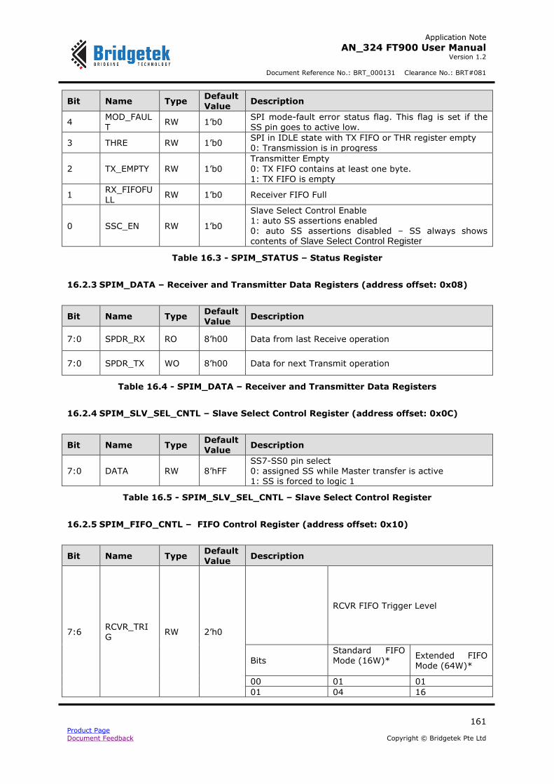
Application Note
AN_324 FT900 User Manual Version 1.2
Document Reference No.: BRT_000131 Clearance No.: BRT#081
161 Product Page Document Feedback Copyright © Bridgetek Pte Ltd
Bit Name Type Default Value
Description
4 MOD_FAULT
RW 1’b0 SPI mode-fault error status flag. This flag is set if the SS pin goes to active low.
3 THRE RW 1’b0 SPI in IDLE state with TX FIFO or THR register empty 0: Transmission is in progress
2 TX_EMPTY RW 1’b0
Transmitter Empty
0: TX FIFO contains at least one byte. 1: TX FIFO is empty
1 RX_FIFOFULL
RW 1’b0 Receiver FIFO Full
0 SSC_EN RW 1’b0
Slave Select Control Enable 1: auto SS assertions enabled 0: auto SS assertions disabled – SS always shows
contents of Slave Select Control Register
Table 16.3 - SPIM_STATUS – Status Register
16.2.3 SPIM_DATA – Receiver and Transmitter Data Registers (address offset: 0x08)
Bit Name Type Default Value
Description
7:0 SPDR_RX RO 8’h00 Data from last Receive operation
7:0 SPDR_TX WO 8’h00 Data for next Transmit operation
Table 16.4 - SPIM_DATA – Receiver and Transmitter Data Registers
16.2.4 SPIM_SLV_SEL_CNTL – Slave Select Control Register (address offset: 0x0C)
Bit Name Type Default Value
Description
7:0 DATA RW 8’hFF SS7-SS0 pin select 0: assigned SS while Master transfer is active 1: SS is forced to logic 1
Table 16.5 - SPIM_SLV_SEL_CNTL – Slave Select Control Register
16.2.5 SPIM_FIFO_CNTL – FIFO Control Register (address offset: 0x10)
Bit Name Type Default Value
Description
7:6 RCVR_TRIG
RW 2’h0
RCVR FIFO Trigger Level
Bits Standard FIFO Mode (16W)*
Extended FIFO Mode (64W)*
00 01 01
01 04 16
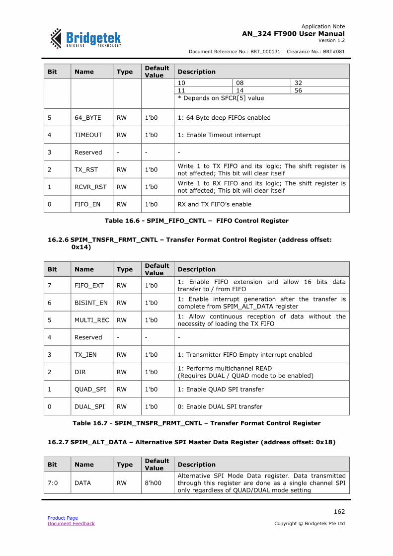
Application Note
AN_324 FT900 User Manual Version 1.2
Document Reference No.: BRT_000131 Clearance No.: BRT#081
162 Product Page Document Feedback Copyright © Bridgetek Pte Ltd
Bit Name Type Default Value
Description
10 08 32
11 14 56
* Depends on SFCR[5] value
5 64_BYTE RW 1’b0 1: 64 Byte deep FIFOs enabled
4 TIMEOUT RW 1’b0 1: Enable Timeout interrupt
3 Reserved - - -
2 TX_RST RW 1’b0 Write 1 to TX FIFO and its logic; The shift register is not affected; This bit will clear itself
1 RCVR_RST RW 1’b0 Write 1 to RX FIFO and its logic; The shift register is
not affected; This bit will clear itself
0 FIFO_EN RW 1’b0 RX and TX FIFO’s enable
Table 16.6 - SPIM_FIFO_CNTL – FIFO Control Register
16.2.6 SPIM_TNSFR_FRMT_CNTL – Transfer Format Control Register (address offset:
0x14)
Bit Name Type Default
Value Description
7 FIFO_EXT RW 1’b0 1: Enable FIFO extension and allow 16 bits data transfer to / from FIFO
6 BISINT_EN RW 1’b0 1: Enable interrupt generation after the transfer is complete from SPIM_ALT_DATA register
5 MULTI_REC RW 1’b0 1: Allow continuous reception of data without the
necessity of loading the TX FIFO
4 Reserved - - -
3 TX_IEN RW 1’b0 1: Transmitter FIFO Empty interrupt enabled
2 DIR RW 1’b0 1: Performs multichannel READ
(Requires DUAL / QUAD mode to be enabled)
1 QUAD_SPI RW 1’b0 1: Enable QUAD SPI transfer
0 DUAL_SPI RW 1’b0 0: Enable DUAL SPI transfer
Table 16.7 - SPIM_TNSFR_FRMT_CNTL – Transfer Format Control Register
16.2.7 SPIM_ALT_DATA – Alternative SPI Master Data Register (address offset: 0x18)
Bit Name Type Default Value
Description
7:0 DATA RW 8’h00 Alternative SPI Mode Data register. Data transmitted through this register are done as a single channel SPI only regardless of QUAD/DUAL mode setting

Application Note
AN_324 FT900 User Manual Version 1.2
Document Reference No.: BRT_000131 Clearance No.: BRT#081
163 Product Page Document Feedback Copyright © Bridgetek Pte Ltd
Table 16.8 - SPIM_ALT_DATA – Alternative SPI Master Data Register
16.2.8 SPIM_RX_FIFO_COUNT – SPI Master RX FIFO Count Register (address offset:
0x1C)
Bit Name Type Default Value
Description
7:0 DATA RW 8’h00
The number of bytes available in the RX FIFO. Note that the counter can only count up to 63, then rolls back to 0. If it is 0 and SPI_FLAG bit is 1, it means
there are 64 bytes in the FIFO
Table 16.9 - SPIM_RX_FIFO_COUNT – SPI Master RX FIFO Count Register
Application Note
AN_324 FT900 User Manual Version 1.2
Document Reference No.: BRT_000131 Clearance No.: BRT#081
164 Product Page Document Feedback Copyright © Bridgetek Pte Ltd
17 SPI Slaves
There are two independent SPI slaves in the device. Listed below are the key features of the SPI slaves:
Full duplex synchronous serial data transfer
Two modes of operations: SPI mode and FIFO mode
FIFO size of 64 bytes
System error detection
Interrupt generation
Four transfer formats supported
17.1 Register Summary
Listed below are the registers with their offset from the base addresses (0x102C0 and 0x102E0
respectively). All registers can only be accessed via Double-Word (32-bit) mode. However, the least significant byte of the FIFO can be accessed via Byte (8-bit) mode. This facilitates fast byte oriented operations.
Address
Offset
Register Default
value
References
0x00 SPIS_CNTL – Control Register 0x04 Section 17.2.1
0x04 SPIS_STATUS – Status Register 0x00 Section 17.2.2
0x08 SPIS_DATA – Receiver and Transmitter Data
Registers
0x00 Section 17.2.3
0x0C SPIS_SLV_SEL_CNTL – Slave Select Control
Register 0x00 Section 17.2.4
0x10 SPIS_FIFO_CNTL – FIFO Control Register 0x00 Section 17.2.5
0x14 SPIS_TNSFR_FRMT_CNTL – Transfer Format
Control Register 0x00 Section 17.2.6
0x18 SPIS_ALT_DATA – Alternative SPI Slave Data Register
Section 17.2.7
0x1C SPIS_RX_FIFO_COUNT – SPI Slave RX FIFO Count Register
0x00 Section 17.2.8
Table 17.1 - Overview of SPI Slave Registers
17.2 Register Details
17.2.1 SPIS_CNTL – Control Register (address offset: 0x00)
Bit Name Type Default Value
Description
7 SP_IE RW 1’b0 1: To enable SPI Slave interrupt
6 SP_E RW 1’b0 SPI System enable; 1 to enable.

Application Note
AN_324 FT900 User Manual Version 1.2
Document Reference No.: BRT_000131 Clearance No.: BRT#081
165 Product Page Document Feedback Copyright © Bridgetek Pte Ltd
Bit Name Type Default Value
Description
5 SP_R2 RW 1’b0 See table at SP_R1 and SP_R0
4 Reserved - - -
3 CLK_POL RW 1’b0 Clock polarity select 0: High level; SCK idles Low 1: Low level; SCK idles high
2 CLK_PHA RW 1’b1
Clock phase 0: Shift Data Out on Falling edge; capture Data In on Rising edge 1: Shift Data Out on Rising edge; capture Data In on Falling edge
1:0 SP_R[1:0] RW 1’b0 Set SP_R2/1/0 value to 0 if the SPI master is operating
at high speed. Otherwise, set it to a non-zero value.
Table 17.2 - SPIS_CNTL – Control Register
17.2.2 SPIS_STATUS – Status Register (address offset: 0x04)
Bit Name Type Default Value
Description
7
SPI_FLAG RW 1’b0 Interrupt request; this flag is automatically set to one at the end of an SPI transfer
6 WR_COL RW 1’b0 Write collision error status flag. The flag is automatically set if the SPDR is written when the TX
register is full (in FIFO Mode when the TX FIFO is full)
5 SPI_BIS RW 1’b0 Indicates end of transmission from SPIS_ALT_DATA register. This flag can generate an interrupt if enabled by SPIS_TNSFR_FRMT_CNTL[6]=1
4 Reserved - - -
3 THRE RW 1’b0 SPI in IDLE state with TX FIFO or THR register empty 0: Transmission is in progress
2 TX_EMPTY RW 1’b0 Transmitter Empty 0: TX FIFO contains at least one byte.
1: TX FIFO is empty
1 RX_FIFOFULL
RW 1’b0 Receiver FIFO Full
0 SSC_EN RW 1’b0
Slave Select Control Enable 1: auto SS assertions enabled 0: auto SS assertions disabled – SS always shows
contents of Slave Select Control Register
Table 17.3 - SPIS_STATUS – Status Register

Application Note
AN_324 FT900 User Manual Version 1.2
Document Reference No.: BRT_000131 Clearance No.: BRT#081
166 Product Page Document Feedback Copyright © Bridgetek Pte Ltd
17.2.3 SPIS_DATA – Receiver and Transmitter Data Registers (address offset: 0x08)
Bit Name Type Default Value
Description
7:0 SPDR_RX RO 8’h00 Data from last Receive operation
7:0 SPDR_TX WO 8’h00 Data for next Transmit operation
Table 17.4 - SPIS_DATA – Receiver and Transmitter Data Registers
17.2.4 SPIS_SLV_SEL_CNTL – Slave Select Control Register (address offset: 0x0C)
Bit Name Type Default
Value Description
7:0 Reserved - - -
Table 17.5 - SPIS_SLV_SEL_CNTL – Slave Select Control Register
17.2.5 SPIS_FIFO_CNTL – FIFO Control Register (address offset: 0x10)
Bit Name Type Default Value
Description
7:6 RCVR_TRIG
RW 2’h0
RCVR FIFO Trigger Level
Bits Standard FIFO Mode (16W)*
Extended FIFO Mode (64W)*
00 01 01
01 04 16
10 08 32
11 14 56
* Depends on SFCR[5] value
5 64_BYTE RW 1’b0 1: 64 Byte deep FIFOs enabled
4 TIMEOUT RW 1’b0 1: Enable Timeout interrupt
3 Reserved - - -
2 TX_RST RW 1’b0 Write 1 to TX FIFO and its logic; The shift register is not affected; This bit will clear itself
1 RCVR_RST RW 1’b0 Write 1 to RX FIFO and its logic; The shift register is not affected; This bit will clear itself
0 FIFO_EN RW 1’b0 RX and TX FIFO’s enable
Table 17.6 - SPIS_FIFO_CNTL – FIFO Control Register

Application Note
AN_324 FT900 User Manual Version 1.2
Document Reference No.: BRT_000131 Clearance No.: BRT#081
167 Product Page Document Feedback Copyright © Bridgetek Pte Ltd
17.2.6 SPIS_TNSFR_FRMT_CNTL – Transfer Format Control Register (address offset: 0x14)
Bit Name Type Default
Value Description
7 FIFO_EXT RW 1’b0 1: Enable FIFO extension and allow 16 bits data transfer to / from FIFO
6 BISINT_EN RW 1’b0 1: Enable interrupt generation after transfer is complete from SPIS_ALT_DATA register
5 MULTI_REC RW 1’b0 1: Allow continuous reception of data without the necessity of loading the TX FIFO
4 Reserved - - -
3 TX_IEN RW 1’b0 1: Transmitter FIFO Empty interrupt enabled
2:0 Reserved - - -
Table 17.7 - SPIS_TNSFR_FRMT_CNTL – Transfer Format Control Register
17.2.7 SPIS_ALT_DATA – Alternative SPI Slave Data Register (address offset: 0x18)
Bit Name Type Default Value
Description
7:0 DATA RW 8’h00 Alternative SPI Mode Data register. Data transmitted through this register are done as a single channel SPI only, regardless of QUAD/DUAL mode setting
Table 17.8 - SPIS_ALT_DATA – Alternative SPI Slave Data Register
17.2.8 SPIS_RX_FIFO_COUNT – SPI Slave RX FIFO Count Register (address offset:
0x1C)
Bit Name Type Default
Value Description
7:0 DATA RW 8’h00
The number of bytes available in the RX FIFO. Note that the counter can only count up to 63, then rolls back to 0. If it is 0 and SPI_FLAG bit is 1, it means there are 64 bytes in the FIFO
Table 17.9 - SPIS_RX_FIFO_COUNT – SPI Slave RX FIFO Count Register
Application Note
AN_324 FT900 User Manual Version 1.2
Document Reference No.: BRT_000131 Clearance No.: BRT#081
168 Product Page Document Feedback Copyright © Bridgetek Pte Ltd
18 I2C Master
The I2C Master conforms to v2.1 and v3.0 of the I2C specification.
Listed below are the key features supported by the I2C master:
Supports Standard Speed Mode (up to 100kb/s)
Supports Fast mode (up to 400kb/s)
Supports Fast-plus mode (up to 1Mb/s)
Supports High-speed mode (up to 3.4Mb/s)
Performs arbitration and clock synchronisation
Supports multi-master systems
Supports both 7-bit and 10-bit address modes
Supports interrupt generation
Supports FIFO mode
18.1 Register Summary
Listed below are the registers with their offset from the base address (0x10300). All registers can only be accessed via Byte (8-bit) mode.
Address Offset
Register Default value
References
0x00 I2CM_SLV_ADDR - Slave Address Register 0x00 Section 18.2.1
0x01 I2CM_CNTL - Control Register 0x00 Section 18.2.2
0x01 I2CM_STATUS - Status Register 0x20 Section 18.2.3
0x02 I2CM_DATA - Receive / Transmit Data Register 0x00 Section 18.2.4
0x03 I2CM_TIME_PERIOD - Timer Period Register 0x01 Section 18.2.5
0x03 I2CM_HS_TIME_PERIOD - High Speed Timer Period Register
0x01 Section 18.2.6
0x04 I2CM_FIFO_LEN - FIFO Mode Byte Length 0x00 Section 18.2.7
0x05 I2CM_FIFO_INT_ENABLE - FIFO Mode Interrupt
Enable
0x00 Section 18.2.8
0x06 I2CM_FIFO_INT_PEND - FIFO Mode Interrupt
Pending
0x00 Section 18.2.9
0x07 I2CM_FIFO_DATA - FIFO Data Register 0x00 Section 18.2.10
0x08 I2CM_TRIG - Trigger Register 0x00 Section 18.2.11
Table 18.1 - Overview of I2C Master Registers

Application Note
AN_324 FT900 User Manual Version 1.2
Document Reference No.: BRT_000131 Clearance No.: BRT#081
169 Product Page Document Feedback Copyright © Bridgetek Pte Ltd
18.2 Register Details
18.2.1 I2CM_SLV_ADDR – Slave Address Register (address offset: 0x00)
Bit Name Type Default
Value Description
7:1 SLV_ADDR RW 7’h00 This is 7-bit address bits
0 RX_OP RW 1’b0 0: next operation is a transmission 1: next operation is a reception
Table 18.2 - I2CM_SLV_ADDR – Slave Address Register
18.2.2 I2CM_CNTL – Control Register (address offset: 0x01)
Bit Name Type Default Value
Description
7 I2C_RST WO 1’b0 Resets the whole I2C Master controller.
6 SLV_RST WO 1’b0
If set together with the RUN bit, the master will
generate 9 I2C clocks without generating the START condition to recover a blocking Slave device to a known state. A STOP condition will be generated. This bit will be automatically cleared.
5 ADDR WO 1’b0 Setting this together with the RUN bit will cause the generation of a START condition and transmission of a
Slave address.
4 HS WO 1’b0 Setting this together with the RUN bit switches the Bus
controller into high-speed mode.
3 ACK WO 1’b0
This bit should normally be set when the Master is in the receiver mode to generate ACK. It must be cleared
when the master requires no further data from the Slave transmitter.
2 STOP WO 1’b0 Setting this will cause the STOP condition to be generated.
1 START WO 1’b0 Setting this will cause the START or Repeated START condition to be generated.
0 RUN WO 1’b0 Setting this will cause the Bus controller to be active.
Table 18.3 - I2CM_CNTL – Control Register
18.2.3 I2CM_STATUS – Status Register (address offset: 0x01)
Bit Name Type Default Value
Description
7 Reserved - - -
6 BUS_BUSY RO 1’b0 1: indicates the Bus is Busy, and access is not possible.
It’s reset by START/STOP conditions.

Application Note
AN_324 FT900 User Manual Version 1.2
Document Reference No.: BRT_000131 Clearance No.: BRT#081
170 Product Page Document Feedback Copyright © Bridgetek Pte Ltd
Bit Name Type Default Value
Description
5 I2C_IDLE RO 1’b1 1: indicates the Bus controller is in the IDLE state.
4 ARB_LOST RO 1’b0 1: indicates that during the last operation the Bus controller lost the arbitration
3 DATA_ACK RO 1’b0 1: indicates that during the last transmit operation data wasn’t acknowledged.
2 ADDR_ACK RO 1’b0 1: indicates that during the last operation the slave
address wasn’t acknowledged.
1 I2C_ERR RO 1’b0 1: indicates an error occurred during the last operation – ARB_LOST, DATA_ACK or ADDR_ACK
0 I2C_BUSY RO 1’b0 1: indicates that the Bus controller is receiving / transmitting data on the bus; other status bits of the Status register are not valid.
Table 18.4 - I2CM_STATUS – Status Register
18.2.4 I2CM_DATA – Receive / Transmit Data Register (address offset: 0x02)
Bit Name Type Default Value
Description
7:0 DATA RW 8’h00
When read, this is the data received in the last
transaction. When written, this is the data to be transmitted in the next transaction.
Table 18.5 - I2CM_DATA – Receive / Transmit Data Register
18.2.5 I2CM_TIME_PERIOD – Timer Period Register (address offset: 0x03)
Bit Name Type Default Value
Description
7 TIME_ENB RW 1’b0 Cleared to use this register.
6:0 SCL_LP RW 7’h01
Frequency scaler used in STANDARD_FAST and FAST_PLUS modes. The value is appended with a 1 at LSB to make it 8-bit. SCL_PERIOD = (SCL_LP[6] * 128 + SCL_LP[5] * 64 +
SCL_LP[4] * 32 + SCL_LP[3] * 16 + SCL_LP[2] * 8 + SCL_LP[1] * 4 + SCL_LP[0] * 2 + 1) * CLK_PERIOD
Table 18.6 - I2CM_TIME_PERIOD – Timer Period Register
18.2.6 I2CM_HS_TIME_PERIOD – High Speed Timer Period Register (address offset: 0x03)
Bit Name Type Default Value
Description
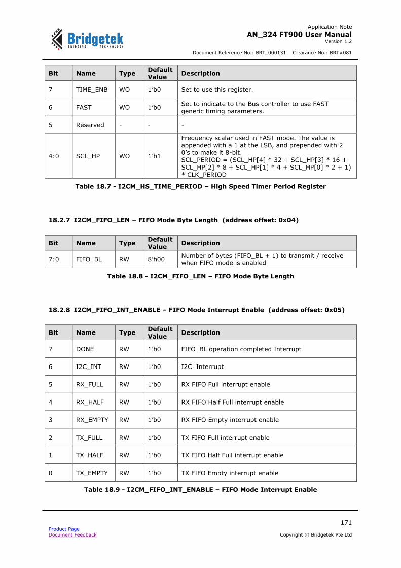
Application Note
AN_324 FT900 User Manual Version 1.2
Document Reference No.: BRT_000131 Clearance No.: BRT#081
171 Product Page Document Feedback Copyright © Bridgetek Pte Ltd
Bit Name Type Default Value
Description
7 TIME_ENB WO 1’b0 Set to use this register.
6 FAST WO 1’b0 Set to indicate to the Bus controller to use FAST generic timing parameters.
5 Reserved - - -
4:0 SCL_HP WO 1’b1
Frequency scalar used in FAST mode. The value is appended with a 1 at the LSB, and prepended with 2 0’s to make it 8-bit. SCL_PERIOD = (SCL_HP[4] * 32 + SCL_HP[3] * 16 + SCL_HP[2] * 8 + SCL_HP[1] * 4 + SCL_HP[0] * 2 + 1) * CLK_PERIOD
Table 18.7 - I2CM_HS_TIME_PERIOD – High Speed Timer Period Register
18.2.7 I2CM_FIFO_LEN – FIFO Mode Byte Length (address offset: 0x04)
Bit Name Type Default Value
Description
7:0 FIFO_BL RW 8’h00 Number of bytes (FIFO_BL + 1) to transmit / receive when FIFO mode is enabled
Table 18.8 - I2CM_FIFO_LEN – FIFO Mode Byte Length
18.2.8 I2CM_FIFO_INT_ENABLE – FIFO Mode Interrupt Enable (address offset: 0x05)
Bit Name Type Default Value
Description
7 DONE RW 1’b0 FIFO_BL operation completed Interrupt
6 I2C_INT RW 1’b0 I2C Interrupt
5 RX_FULL RW 1’b0 RX FIFO Full interrupt enable
4 RX_HALF RW 1’b0 RX FIFO Half Full interrupt enable
3 RX_EMPTY RW 1’b0 RX FIFO Empty interrupt enable
2 TX_FULL RW 1’b0 TX FIFO Full interrupt enable
1 TX_HALF RW 1’b0 TX FIFO Half Full interrupt enable
0 TX_EMPTY RW 1’b0 TX FIFO Empty interrupt enable
Table 18.9 - I2CM_FIFO_INT_ENABLE – FIFO Mode Interrupt Enable
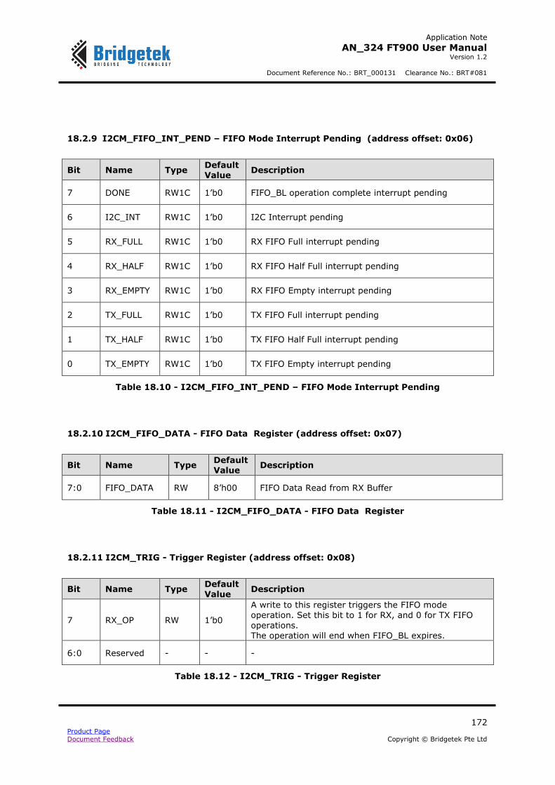
Application Note
AN_324 FT900 User Manual Version 1.2
Document Reference No.: BRT_000131 Clearance No.: BRT#081
172 Product Page Document Feedback Copyright © Bridgetek Pte Ltd
18.2.9 I2CM_FIFO_INT_PEND – FIFO Mode Interrupt Pending (address offset: 0x06)
Bit Name Type Default Value
Description
7 DONE RW1C 1’b0 FIFO_BL operation complete interrupt pending
6 I2C_INT RW1C 1’b0 I2C Interrupt pending
5 RX_FULL RW1C 1’b0 RX FIFO Full interrupt pending
4 RX_HALF RW1C 1’b0 RX FIFO Half Full interrupt pending
3 RX_EMPTY RW1C 1’b0 RX FIFO Empty interrupt pending
2 TX_FULL RW1C 1’b0 TX FIFO Full interrupt pending
1 TX_HALF RW1C 1’b0 TX FIFO Half Full interrupt pending
0 TX_EMPTY RW1C 1’b0 TX FIFO Empty interrupt pending
Table 18.10 - I2CM_FIFO_INT_PEND – FIFO Mode Interrupt Pending
18.2.10 I2CM_FIFO_DATA - FIFO Data Register (address offset: 0x07)
Bit Name Type Default Value
Description
7:0 FIFO_DATA RW 8’h00 FIFO Data Read from RX Buffer
Table 18.11 - I2CM_FIFO_DATA - FIFO Data Register
18.2.11 I2CM_TRIG - Trigger Register (address offset: 0x08)
Bit Name Type Default Value
Description
7 RX_OP RW 1’b0
A write to this register triggers the FIFO mode
operation. Set this bit to 1 for RX, and 0 for TX FIFO
operations. The operation will end when FIFO_BL expires.
6:0 Reserved - - -
Table 18.12 - I2CM_TRIG - Trigger Register
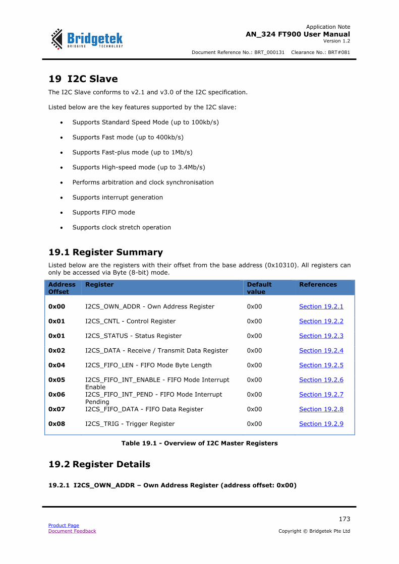
Application Note
AN_324 FT900 User Manual Version 1.2
Document Reference No.: BRT_000131 Clearance No.: BRT#081
173 Product Page Document Feedback Copyright © Bridgetek Pte Ltd
19 I2C Slave
The I2C Slave conforms to v2.1 and v3.0 of the I2C specification.
Listed below are the key features supported by the I2C slave:
Supports Standard Speed Mode (up to 100kb/s)
Supports Fast mode (up to 400kb/s)
Supports Fast-plus mode (up to 1Mb/s)
Supports High-speed mode (up to 3.4Mb/s)
Performs arbitration and clock synchronisation
Supports interrupt generation
Supports FIFO mode
Supports clock stretch operation
19.1 Register Summary
Listed below are the registers with their offset from the base address (0x10310). All registers can only be accessed via Byte (8-bit) mode.
Address Offset
Register Default value
References
0x00 I2CS_OWN_ADDR - Own Address Register 0x00 Section 19.2.1
0x01 I2CS_CNTL - Control Register 0x00 Section 19.2.2
0x01 I2CS_STATUS - Status Register 0x00 Section 19.2.3
0x02 I2CS_DATA - Receive / Transmit Data Register 0x00 Section 19.2.4
0x04 I2CS_FIFO_LEN - FIFO Mode Byte Length 0x00 Section 19.2.5
0x05 I2CS_FIFO_INT_ENABLE - FIFO Mode Interrupt Enable
0x00 Section 19.2.6
0x06 I2CS_FIFO_INT_PEND - FIFO Mode Interrupt
Pending
0x00 Section 19.2.7
0x07 I2CS_FIFO_DATA - FIFO Data Register 0x00 Section 19.2.8
0x08 I2CS_TRIG - Trigger Register 0x00 Section 19.2.9
Table 19.1 - Overview of I2C Master Registers
19.2 Register Details
19.2.1 I2CS_OWN_ADDR – Own Address Register (address offset: 0x00)
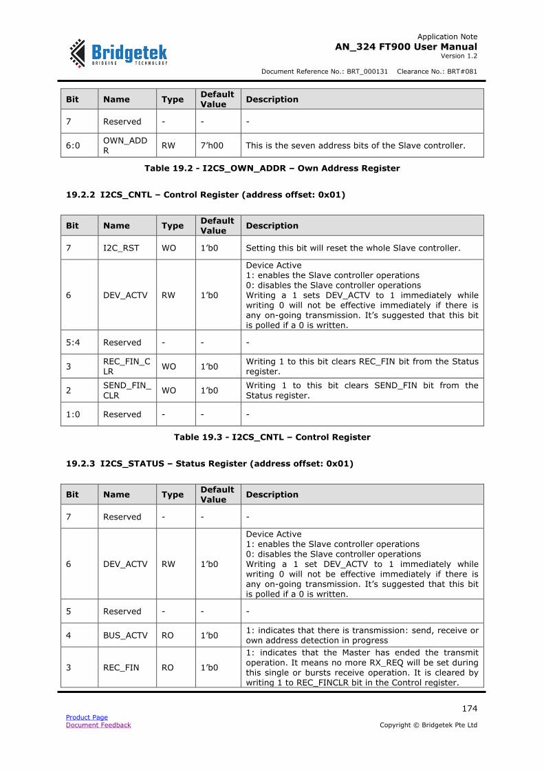
Application Note
AN_324 FT900 User Manual Version 1.2
Document Reference No.: BRT_000131 Clearance No.: BRT#081
174 Product Page Document Feedback Copyright © Bridgetek Pte Ltd
Bit Name Type Default Value
Description
7 Reserved - - -
6:0 OWN_ADDR
RW 7’h00 This is the seven address bits of the Slave controller.
Table 19.2 - I2CS_OWN_ADDR – Own Address Register
19.2.2 I2CS_CNTL – Control Register (address offset: 0x01)
Bit Name Type Default Value
Description
7 I2C_RST WO 1’b0 Setting this bit will reset the whole Slave controller.
6 DEV_ACTV RW 1’b0
Device Active 1: enables the Slave controller operations 0: disables the Slave controller operations Writing a 1 sets DEV_ACTV to 1 immediately while writing 0 will not be effective immediately if there is any on-going transmission. It’s suggested that this bit is polled if a 0 is written.
5:4 Reserved - - -
3 REC_FIN_CLR
WO 1’b0 Writing 1 to this bit clears REC_FIN bit from the Status register.
2 SEND_FIN_
CLR WO 1’b0
Writing 1 to this bit clears SEND_FIN bit from the
Status register.
1:0 Reserved - - -
Table 19.3 - I2CS_CNTL – Control Register
19.2.3 I2CS_STATUS – Status Register (address offset: 0x01)
Bit Name Type Default Value
Description
7 Reserved - - -
6 DEV_ACTV RW 1’b0
Device Active 1: enables the Slave controller operations 0: disables the Slave controller operations Writing a 1 set DEV_ACTV to 1 immediately while writing 0 will not be effective immediately if there is any on-going transmission. It’s suggested that this bit is polled if a 0 is written.
5 Reserved - - -
4 BUS_ACTV RO 1’b0 1: indicates that there is transmission: send, receive or own address detection in progress
3 REC_FIN RO 1’b0
1: indicates that the Master has ended the transmit
operation. It means no more RX_REQ will be set during this single or bursts receive operation. It is cleared by writing 1 to REC_FINCLR bit in the Control register.
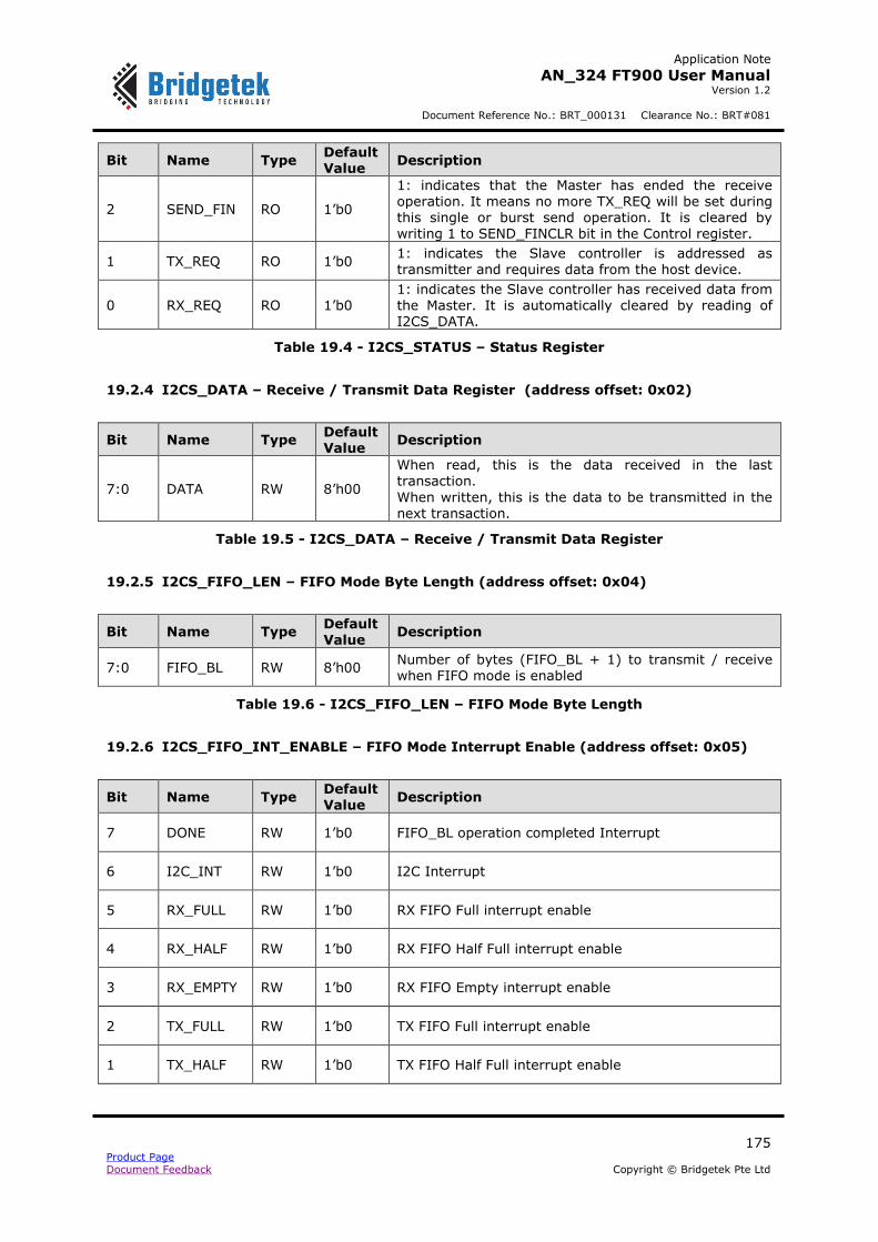
Application Note
AN_324 FT900 User Manual Version 1.2
Document Reference No.: BRT_000131 Clearance No.: BRT#081
175 Product Page Document Feedback Copyright © Bridgetek Pte Ltd
Bit Name Type Default Value
Description
2 SEND_FIN RO 1’b0
1: indicates that the Master has ended the receive operation. It means no more TX_REQ will be set during this single or burst send operation. It is cleared by writing 1 to SEND_FINCLR bit in the Control register.
1 TX_REQ RO 1’b0 1: indicates the Slave controller is addressed as transmitter and requires data from the host device.
0 RX_REQ RO 1’b0 1: indicates the Slave controller has received data from the Master. It is automatically cleared by reading of I2CS_DATA.
Table 19.4 - I2CS_STATUS – Status Register
19.2.4 I2CS_DATA – Receive / Transmit Data Register (address offset: 0x02)
Bit Name Type Default Value
Description
7:0 DATA RW 8’h00
When read, this is the data received in the last transaction.
When written, this is the data to be transmitted in the next transaction.
Table 19.5 - I2CS_DATA – Receive / Transmit Data Register
19.2.5 I2CS_FIFO_LEN – FIFO Mode Byte Length (address offset: 0x04)
Bit Name Type Default Value
Description
7:0 FIFO_BL RW 8’h00 Number of bytes (FIFO_BL + 1) to transmit / receive when FIFO mode is enabled
Table 19.6 - I2CS_FIFO_LEN – FIFO Mode Byte Length
19.2.6 I2CS_FIFO_INT_ENABLE – FIFO Mode Interrupt Enable (address offset: 0x05)
Bit Name Type Default Value
Description
7 DONE RW 1’b0 FIFO_BL operation completed Interrupt
6 I2C_INT RW 1’b0 I2C Interrupt
5 RX_FULL RW 1’b0 RX FIFO Full interrupt enable
4 RX_HALF RW 1’b0 RX FIFO Half Full interrupt enable
3 RX_EMPTY RW 1’b0 RX FIFO Empty interrupt enable
2 TX_FULL RW 1’b0 TX FIFO Full interrupt enable
1 TX_HALF RW 1’b0 TX FIFO Half Full interrupt enable
Application Note
AN_324 FT900 User Manual Version 1.2
Document Reference No.: BRT_000131 Clearance No.: BRT#081
176 Product Page Document Feedback Copyright © Bridgetek Pte Ltd
Bit Name Type Default Value
Description
0 TX_EMPTY RW 1’b0 TX FIFO Empty interrupt enable
Table 19.7 - I2CS_FIFO_INT_ENABLE – FIFO Mode Interrupt Enable
19.2.7 I2CS_FIFO_INT_PEND – FIFO Mode Interrupt Pending (address offset: 0x06)
Bit Name Type Default
Value Description
7 DONE RW1C 1’b0 FIFO_BL operation complete interrupt pending
6 I2C_INT RW1C 1’b0 I2C Interrupt pending
5 RX_FULL RW1C 1’b0 RX FIFO Full interrupt pending
4 RX_HALF RW1C 1’b0 RX FIFO Half Full interrupt pending
3 RX_EMPTY RW1C 1’b0 RX FIFO Empty interrupt pending
2 TX_FULL RW1C 1’b0 TX FIFO Full interrupt pending
1 TX_HALF RW1C 1’b0 TX FIFO Half Full interrupt pending
0 TX_EMPTY RW1C 1’b0 TX FIFO Empty interrupt pending
Table 19.8 - I2CS_FIFO_INT_PEND – FIFO Mode Interrupt Pending
19.2.8 I2CS_FIFO_DATA - FIFO Data Register (address offset: 0x07)
Bit Name Type Default Value
Description
7:0 FIFO_DATA RO 8’h00 FIFO Data Read from the RX Buffer
Table 19.9 - I2CS_FIFO_DATA - FIFO Data Register
19.2.9 I2CS_TRIG - Trigger Register (address offset: 0x08)
Bit Name Type Default Value
Description
7 RX_OP RW 1’b0
A write to this register triggers the FIFO mode operation. Set this bit to 1 for RX, and 0 for TX FIFO
operations.
The operation will end when FIFO_BL expires.
6:0 Reserved - - -
Table 19.10 - I2CS_TRIG - Trigger Register
Application Note
AN_324 FT900 User Manual Version 1.2
Document Reference No.: BRT_000131 Clearance No.: BRT#081
177 Product Page Document Feedback Copyright © Bridgetek Pte Ltd
20 RTC
This is a Real Time Clock (RTC) running off a dedicated 32.768 kHz oscillator. It is powered by the internal 1.2V regulator.
20.1 Register Summary
Listed below are the registers with their offset from the base address (0x10280). All registers can be accessed via Double-Word (32-bit) mode.
Address Offset
Register Default value
References
0x00 RTC_CCVR - Current Counter Value Register 0x00000000 Section 20.2.1
0x04 RTC_CMR - Counter Match Register 0x00000000 Section 20.2.2
0x08 RTC_CLR - Counter Load Register 0x00000000 Section 20.2.3
0x0C RTC_CCR - Counter Control Register 0x00000000 Section 20.2.4
0x10 RTC_STAT - Interrupt Status Register 0x00000000 Section 20.2.5
0x14 RTC_RSTAT - Interrupt Raw Status Register 0x00000000 Section 20.2.6
0x18 RTC_EOI - End of Interrupt Register 0x00000000 Section 20.2.7
0x1C RTC_COMP_VERSION - Component Version Register
0x3230332A Section 20.2.8
Table 20.1 - Overview of RTC Registers
20.2 Register Details
20.2.1 RTC_CCVR - Current Counter Value Register (address offset: 0x00)
Bit Name Type Default Value
Description
31:0 DATA RO 32’h0 This is the current value of the internal counter. This value always is read coherently.
Table 20.2 - RTC_CCVR - Current Counter Value Register
20.2.2 RTC_CMR - Counter Match Register (address offset: 0x04)
Bit Name Type Default
Value Description
31:0 DATA RW 32’h0
When the internal counter matches this register, an
interrupt is generated if enabled. When appropriate, this value is written coherently. Only when all relevant bytes have been written will the new value be effective.
Table 20.3 - RTC_CMR - Counter Match Register
Application Note
AN_324 FT900 User Manual Version 1.2
Document Reference No.: BRT_000131 Clearance No.: BRT#081
178 Product Page Document Feedback Copyright © Bridgetek Pte Ltd
20.2.3 RTC_CLR - Counter Load Register (address offset: 0x08)
Bit Name Type Default Value
Description
31:0 DATA RW 32’h0 Loaded in the counter as the loaded value, which is written coherently.
Table 20.4 - RTC_CLR - Counter Load Register
20.2.4 RTC_CCR - Counter Control Register (address offset: 0x0C)
Bit Name Type Default Value
Description
31:4 Reserved - - -
3 RTC_WEN RW 1’h0
Allows the user to force the counter to wrap when a match occurs instead of waiting until the maximum count is reached. 0: wrap disabled
1: wrap enabled
2 RTC_EN RW 1’h0 Allows the user to control counting in the counter. 0: Counter disabled 1: Counter enabled
1 RTC_MASK RW 1’h0 Allows the user to mask a generated interrupt. 0: Interrupt unmasked 1: Interrupt masked
0 RTC_IEN RW 1’h0 Allows the user to disable interrupt generation. 0: Interrupt disabled 1: Interrupt enabled
Table 20.5 - RTC_CCR - - Counter Control Register
20.2.5 RTC_STAT - Interrupt Status Register (address offset: 0x10)
Bit Name Type Default Value
Description
31:1 Reserved - - -
0 RTC_STAT RO 1’h0 This is the masked raw status 0: Interrupt is inactive 1: Interrupt is active (regardless of polarity)
Table 20.6 - RTC_STAT - Interrupt Status Register
20.2.6 RTC_RSTAT - Interrupt Raw Status Register (address offset: 0x14)
Bit Name Type Default
Value Description
Application Note
AN_324 FT900 User Manual Version 1.2
Document Reference No.: BRT_000131 Clearance No.: BRT#081
179 Product Page Document Feedback Copyright © Bridgetek Pte Ltd
31:1 Reserved - - -
0 TC_RSTAT RO 1’h0 0: Interrupt is inactive 1: Interrupt is active (regardless of polarity)
Table 20.7 - RTC_RSTAT - Interrupt Raw Status Register
20.2.7 RTC_EOI - End of Interrupt Register (address offset: 0x18)
Bit Name Type Default Value
Description
31:1 Reserved - - -
0 RTC_EOI RO 1’h0 By reading this location, the match interrupt is cleared. Performing read-to-clear on interrupts, the interrupt is cleared at the end of the read.
Table 20.8 - RTC_EOI - End of Interrupt Register
20.2.8 RTC_COMP_VERSION - Component Version Register (address offset: 0x1C)
Bit Name Type Default Value
Description
31:0 RTC_COMP_ VERSION
RO 32’h3230332A
ASCII value for each number in the version, followed by *. 32_30_33_2A represents the version 2.03*.
Table 20.9 - RTC_COMP_VERSION - Component Version Register
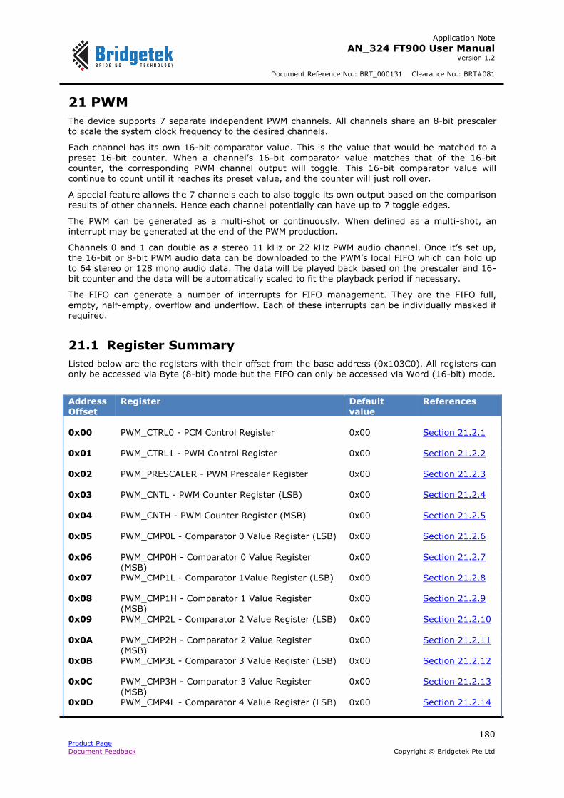
Application Note
AN_324 FT900 User Manual Version 1.2
Document Reference No.: BRT_000131 Clearance No.: BRT#081
180 Product Page Document Feedback Copyright © Bridgetek Pte Ltd
21 PWM
The device supports 7 separate independent PWM channels. All channels share an 8-bit prescaler to scale the system clock frequency to the desired channels.
Each channel has its own 16-bit comparator value. This is the value that would be matched to a preset 16-bit counter. When a channel’s 16-bit comparator value matches that of the 16-bit counter, the corresponding PWM channel output will toggle. This 16-bit comparator value will continue to count until it reaches its preset value, and the counter will just roll over.
A special feature allows the 7 channels each to also toggle its own output based on the comparison results of other channels. Hence each channel potentially can have up to 7 toggle edges.
The PWM can be generated as a multi-shot or continuously. When defined as a multi-shot, an interrupt may be generated at the end of the PWM production.
Channels 0 and 1 can double as a stereo 11 kHz or 22 kHz PWM audio channel. Once it’s set up, the 16-bit or 8-bit PWM audio data can be downloaded to the PWM’s local FIFO which can hold up
to 64 stereo or 128 mono audio data. The data will be played back based on the prescaler and 16-bit counter and the data will be automatically scaled to fit the playback period if necessary.
The FIFO can generate a number of interrupts for FIFO management. They are the FIFO full,
empty, half-empty, overflow and underflow. Each of these interrupts can be individually masked if required.
21.1 Register Summary
Listed below are the registers with their offset from the base address (0x103C0). All registers can only be accessed via Byte (8-bit) mode but the FIFO can only be accessed via Word (16-bit) mode.
Address Offset
Register Default value
References
0x00 PWM_CTRL0 - PCM Control Register 0x00 Section 21.2.1
0x01 PWM_CTRL1 - PWM Control Register 0x00 Section 21.2.2
0x02 PWM_PRESCALER - PWM Prescaler Register 0x00 Section 21.2.3
0x03 PWM_CNTL - PWM Counter Register (LSB) 0x00 Section 21.2.4
0x04 PWM_CNTH - PWM Counter Register (MSB) 0x00 Section 21.2.5
0x05 PWM_CMP0L - Comparator 0 Value Register (LSB) 0x00 Section 21.2.6
0x06 PWM_CMP0H - Comparator 0 Value Register (MSB)
0x00 Section 21.2.7
0x07 PWM_CMP1L - Comparator 1Value Register (LSB) 0x00 Section 21.2.8
0x08 PWM_CMP1H - Comparator 1 Value Register (MSB)
0x00 Section 21.2.9
0x09 PWM_CMP2L - Comparator 2 Value Register (LSB) 0x00 Section 21.2.10
0x0A PWM_CMP2H - Comparator 2 Value Register
(MSB) 0x00 Section 21.2.11
0x0B PWM_CMP3L - Comparator 3 Value Register (LSB) 0x00 Section 21.2.12
0x0C PWM_CMP3H - Comparator 3 Value Register
(MSB)
0x00 Section 21.2.13
0x0D PWM_CMP4L - Comparator 4 Value Register (LSB) 0x00 Section 21.2.14

Application Note
AN_324 FT900 User Manual Version 1.2
Document Reference No.: BRT_000131 Clearance No.: BRT#081
181 Product Page Document Feedback Copyright © Bridgetek Pte Ltd
0x0E PWM_CMP4H - Comparator 4 Value Register (MSB)
0x00 Section 21.2.15
0x0F PWM_CMP5L - Comparator 5 Value Register (LSB) 0x00 Section 21.2.16
0x10 PWM_CMP5H - Comparator 5 Value Register
(MSB)
0x00 Section 21.2.17
0x11 PWM_CMP6L - Comparator 6 Value Register (LSB) 0x00 Section 21.2.18
0x12 PWM_CMP6H - Comparator 6 Value Register
(MSB) 0x00 Section 21.2.19
0x13 PWM_CMP7L - Comparator 7 Value Register (LSB) 0x00 Section 21.2.20
0x14 PWM_CMP7H - Comparator 7 Value Register
(MSB) 0x00 Section 21.2.21
0x15 PWM_TOGGLE0 - Channel 0 OUT Toggle
Comparator Mask Register 0x00 Section 21.2.22
0x16 PWM_TOGGLE1 - Channel 1 OUT Toggle
Comparator Mask Register
0x00 Section 21.2.23
0x17 PWM_TOGGLE2 - Channel 2 OUT Toggle Comparator Mask Register
0x00 Section 21.2.24
0x18 PWM_TOGGLE3 - Channel 3 OUT Toggle Comparator Mask Register
0x00 Section 21.2.25
0x19 PWM_TOGGLE4 - Channel 4 OUT Toggle Comparator Mask Register
0x00 Section 21.2.26
0x1A PWM_TOGGLE5 - Channel 5 OUT Toggle
Comparator Mask Register
0x00 Section 21.2.27
0x1B PWM_TOGGLE6 - Channel 6 OUT Toggle
Comparator Mask Register 0x00 Section 21.2.28
0x1C PWM_TOGGLE7 - Channel 7 OUT Toggle
Comparator Mask Register 0x00 Section 21.2.29
0x1D PWM_OUT_CLR_EN - PWM OUT Clear Enable
Register
0x00 Section 21.2.30
0x1E PWM_CTRL_BL_CMP8 - Control Block CMP8 Value
Register 0x00 Section 21.2.31
0x1F PWM_INIT - PWM Initialization Register 0x00 Section 21.2.32
0x20 PWM_INTMASK - PWM Interrupt Mask Register 0x00 Section 21.2.33
0x21 PWM_INTSTATUS - PWM Interrupt Status Register 0x00 Section 21.2.34
0x22 PWM_SAMPLE_FREQ_H - PWM Data Sampling Frequency High Byte Register
0x56 Section 21.2.35
0x23 PWM_SAMPLE_FREQ_L - PWM Data Sampling Frequency Low Byte Register
0x22 Section 21.2.36
0x24 PCM_VOLUME - PCM Volume Register 0x00 Section 21.2.37
0x3C PWM_BUFFER - PCM Buffer Register 0xXXXX Section 21.2.38
Table 21.1 - Overview of PWM Registers
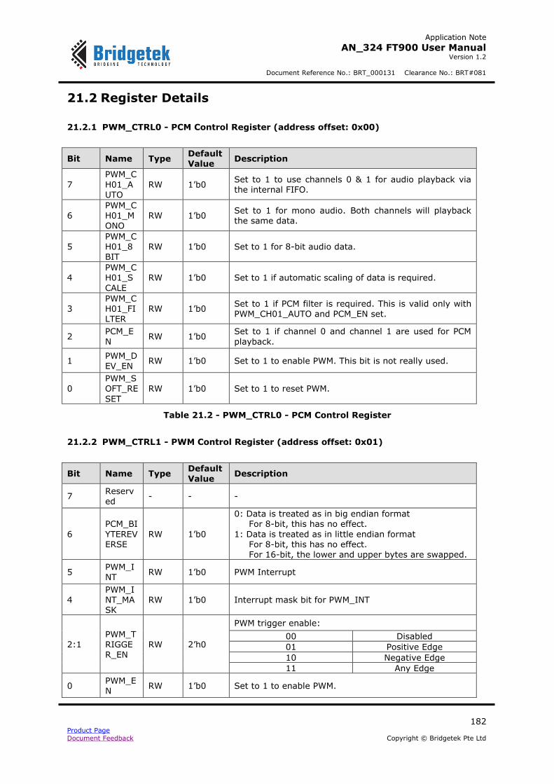
Application Note
AN_324 FT900 User Manual Version 1.2
Document Reference No.: BRT_000131 Clearance No.: BRT#081
182 Product Page Document Feedback Copyright © Bridgetek Pte Ltd
21.2 Register Details
21.2.1 PWM_CTRL0 - PCM Control Register (address offset: 0x00)
Bit Name Type Default Value
Description
7
PWM_C
H01_AUTO
RW 1’b0 Set to 1 to use channels 0 & 1 for audio playback via the internal FIFO.
6 PWM_CH01_MONO
RW 1’b0 Set to 1 for mono audio. Both channels will playback the same data.
5 PWM_CH01_8BIT
RW 1’b0 Set to 1 for 8-bit audio data.
4 PWM_CH01_S
CALE
RW 1’b0 Set to 1 if automatic scaling of data is required.
3 PWM_CH01_FILTER
RW 1’b0 Set to 1 if PCM filter is required. This is valid only with PWM_CH01_AUTO and PCM_EN set.
2 PCM_E
N RW 1’b0
Set to 1 if channel 0 and channel 1 are used for PCM
playback.
1 PWM_DEV_EN
RW 1’b0 Set to 1 to enable PWM. This bit is not really used.
0 PWM_SOFT_RE
SET
RW 1’b0 Set to 1 to reset PWM.
Table 21.2 - PWM_CTRL0 - PCM Control Register
21.2.2 PWM_CTRL1 - PWM Control Register (address offset: 0x01)
Bit Name Type Default
Value Description
7 Reserved
- - -
6
PCM_BI
YTEREVERSE
RW 1’b0
0: Data is treated as in big endian format For 8-bit, this has no effect.
1: Data is treated as in little endian format For 8-bit, this has no effect. For 16-bit, the lower and upper bytes are swapped.
5 PWM_INT
RW 1’b0 PWM Interrupt
4 PWM_INT_MASK
RW 1’b0 Interrupt mask bit for PWM_INT
2:1 PWM_TRIGGER_EN
RW 2’h0
PWM trigger enable:
00 Disabled
01 Positive Edge
10 Negative Edge
11 Any Edge
0 PWM_EN
RW 1’b0 Set to 1 to enable PWM.

Application Note
AN_324 FT900 User Manual Version 1.2
Document Reference No.: BRT_000131 Clearance No.: BRT#081
183 Product Page Document Feedback Copyright © Bridgetek Pte Ltd
Table 21.3 - PWM_CTRL1 - PWM Control Register
21.2.3 PWM_PRESCALER - PWM Prescaler Register (address offset: 0x02)
Bit Name Type Default
Value Description
7:0 PRESCALER
RW 8’h00 8-bit Prescaler value.
Table 21.4 - PWM_PRESCALER - PWM Prescaler Register
21.2.4 PWM_CNTL - PWM Counter Register (LSB) (address offset: 0x03)
Bit Name Type Default
Value Description
7:0 CNT16_LSB
RW 8’h00 16-bit counter LSB.
Table 21.5 - PWM_CNTL - PWM Counter Register (LSB)
21.2.5 PWM_CNTH - PWM Counter Register (MSB) (address offset: 0x04)
Bit Name Type Default Value
Description
7:0 CNT16_MSB
RW 8’h00 16-bit counter MSB.
Table 21.6 - PWM_CNTH - PWM Counter Register (MSB)
21.2.6 PWM_CMP0L - Comparator 0 Value Register (LSB) (address offset: 0x05)
Bit Name Type Default Value
Description
7:0 CMP16_0_LSB
RW 8’h00 LSB of comparator 0 16-bit value.
Table 21.7 - PWM_CMP0L - Comparator 0 Value Register (LSB)
21.2.7 PWM_CMP0H - Comparator 0 Value Register (MSB) (address offset: 0x06)
Bit Name Type Default Value
Description
7:0 CMP16_0_MSB
RW 8’h00 MSB of comparator 0 16-bit value.
Table 21.8 - PWM_CMP0H - Comparator 0 Value Register (MSB)
21.2.8 PWM_CMP1L - Comparator 1 Value Register (LSB) (address offset: 0x07)
Bit Name Type Default Value
Description

Application Note
AN_324 FT900 User Manual Version 1.2
Document Reference No.: BRT_000131 Clearance No.: BRT#081
184 Product Page Document Feedback Copyright © Bridgetek Pte Ltd
7:0 CMP16_1_LSB
RW 8’h00 LSB of comparator 1 16-bit value.
Table 21.9 - PWM_CMP1L - Comparator 1 Value Register (LSB)
21.2.9 PWM_CMP1H - Comparator 1 Value Register (MSB) (address offset: 0x08)
Bit Name Type Default Value
Description
7:0
CMP16
_1_MSB
RW 8’h00 MSB of comparator 1 16-bit value.
Table 21.10 - PWM_CMP1H - Comparator 1 Value Register (MSB)
21.2.10 PWM_CMP2L - Comparator 2 Value Register (LSB) (address offset: 0x09)
Bit Name Type Default Value
Description
7:0 CMP16_2_LSB
RW 8’h00 LSB of comparator 2 16-bit value.
Table 21.11 - PWM_CMP2L - Comparator 2 Value Register (LSB)
21.2.11 PWM_CMP2H - Comparator 2 Value Register (MSB) (address offset: 0x0A)
Bit Name Type Default Value
Description
7:0 CMP16_2_MS
B
RW 8’h00 MSB of comparator 2 16-bit value.
Table 21.12 - PWM_CMP2H - Comparator 2 Value Register (MSB)
21.2.12 PWM_CMP3L - Comparator 3 Value Register (LSB) (address offset: 0x0B)
Bit Name Type Default Value
Description
7:0 CMP16_3_LSB
RW 8’h00 LSB of comparator 3 16-bit value.
Table 21.13 - PWM_CMP3L - Comparator 3 Value Register (LSB)
21.2.13 PWM_CMP3H - Comparator 3 Value Register (MSB) (address offset: 0x0C)
Bit Name Type Default
Value Description
7:0 CMP16_3_MSB
RW 8’h00 MSB of comparator 3 16-bit value.
Table 21.14 - PWM_CMP3H - Comparator 3 Value Register (MSB)

Application Note
AN_324 FT900 User Manual Version 1.2
Document Reference No.: BRT_000131 Clearance No.: BRT#081
185 Product Page Document Feedback Copyright © Bridgetek Pte Ltd
21.2.14 PWM_CMP4L - Comparator 4 Value Register (LSB) (address offset: 0x0D)
Bit Name Type Default Value
Description
7:0 CMP16_4_LSB
RW 8’h00 LSB of comparator 4 16-bit value.
Table 21.15 - PWM_CMP4L - Comparator 4 Value Register (LSB)
21.2.15 PWM_CMP4H - Comparator 4 Value Register (MSB) (address offset: 0x0E)
Bit Name Type Default Value
Description
7:0 CMP16_4_MSB
RW 8’h00 MSB of comparator 4 16-bit value.
Table 21.16 - PWM_CMP4H - Comparator 4 Value Register (MSB)
21.2.16 PWM_CMP5L - Comparator 5 Value Register (LSB) (address offset: 0x0F)
Bit Name Type Default Value
Description
7:0 CMP16_5_LSB
RW 8’h00 LSB of comparator 5 16-bit value.
Table 21.17 - PWM_CMP5L - Comparator 5 Value Register (LSB)
21.2.17 PWM_CMP5H - Comparator 5 Value Register (MSB) (address offset: 0x10)
Bit Name Type Default Value
Description
7:0 CMP16_5_MSB
RW 8’h00 MSB of comparator 5 16-bit value.
Table 21.18 - PWM_CMP5H - Comparator 5 Value Register (MSB)
21.2.18 PWM_CMP6L - Comparator 6 Value Register (LSB) (address offset: 0x11)
Bit Name Type Default
Value Description
7:0 CMP16
_6_LSB RW 8’h00 LSB of comparator 6 16-bit value.
Table 21.19 - PWM_CMP6L - Comparator 6 Value Register (LSB)
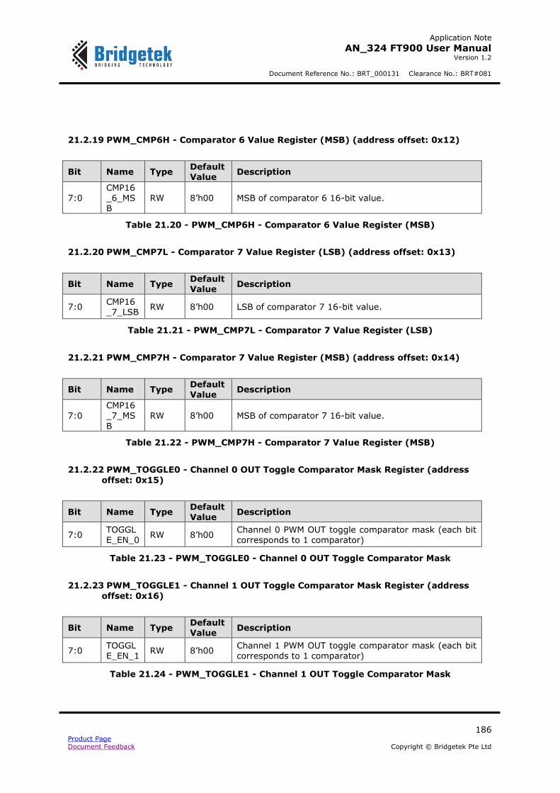
Application Note
AN_324 FT900 User Manual Version 1.2
Document Reference No.: BRT_000131 Clearance No.: BRT#081
186 Product Page Document Feedback Copyright © Bridgetek Pte Ltd
21.2.19 PWM_CMP6H - Comparator 6 Value Register (MSB) (address offset: 0x12)
Bit Name Type Default Value
Description
7:0 CMP16_6_MSB
RW 8’h00 MSB of comparator 6 16-bit value.
Table 21.20 - PWM_CMP6H - Comparator 6 Value Register (MSB)
21.2.20 PWM_CMP7L - Comparator 7 Value Register (LSB) (address offset: 0x13)
Bit Name Type Default Value
Description
7:0 CMP16_7_LSB
RW 8’h00 LSB of comparator 7 16-bit value.
Table 21.21 - PWM_CMP7L - Comparator 7 Value Register (LSB)
21.2.21 PWM_CMP7H - Comparator 7 Value Register (MSB) (address offset: 0x14)
Bit Name Type Default Value
Description
7:0 CMP16_7_MS
B
RW 8’h00 MSB of comparator 7 16-bit value.
Table 21.22 - PWM_CMP7H - Comparator 7 Value Register (MSB)
21.2.22 PWM_TOGGLE0 - Channel 0 OUT Toggle Comparator Mask Register (address
offset: 0x15)
Bit Name Type Default Value
Description
7:0 TOGGLE_EN_0
RW 8’h00 Channel 0 PWM OUT toggle comparator mask (each bit corresponds to 1 comparator)
Table 21.23 - PWM_TOGGLE0 - Channel 0 OUT Toggle Comparator Mask
21.2.23 PWM_TOGGLE1 - Channel 1 OUT Toggle Comparator Mask Register (address
offset: 0x16)
Bit Name Type Default Value
Description
7:0 TOGGLE_EN_1
RW 8’h00 Channel 1 PWM OUT toggle comparator mask (each bit corresponds to 1 comparator)
Table 21.24 - PWM_TOGGLE1 - Channel 1 OUT Toggle Comparator Mask

Application Note
AN_324 FT900 User Manual Version 1.2
Document Reference No.: BRT_000131 Clearance No.: BRT#081
187 Product Page Document Feedback Copyright © Bridgetek Pte Ltd
21.2.24 PWM_TOGGLE2 - Channel 2 OUT Toggle Comparator Mask Register (address offset: 0x17)
Bit Name Type Default Value
Description
7:0 TOGGLE_EN_2
RW 8’h00 Channel 2 PWM OUT toggle comparator mask (each bit corresponds to 1 comparator)
Table 21.25 - PWM_TOGGLE2 - Channel 2 OUT Toggle Comparator Mask Register
21.2.25 PWM_TOGGLE3 - Channel 3 OUT Toggle Comparator Mask Register (address
offset: 0x18)
Bit Name Type Default
Value Description
7:0 TOGGLE_EN_3
RW 8’h00 Channel 3 PWM OUT toggle comparator mask (each bit corresponds to 1 comparator)
Table 21.26 - PWM_TOGGLE3 - Channel 3 OUT Toggle Comparator Mask Register
21.2.26 PWM_TOGGLE4 - Channel 4 OUT Toggle Comparator Mask Register (address offset: 0x19)
Bit Name Type Default Value
Description
7:0 TOGGL
E_EN_4 RW 8’h00
Channel 4 PWM OUT toggle comparator mask (each bit
corresponds to 1 comparator)
Table 21.27 - PWM_TOGGLE4 - Channel 4 OUT Toggle Comparator Mask Register
21.2.27 PWM_TOGGLE5 - Channel 5 OUT Toggle Comparator Mask Register (address
offset: 0x1A)
Bit Name Type Default
Value Description
7:0 TOGGLE_EN_5
RW 8’h00 Channel 5 PWM OUT toggle comparator mask (each bit corresponds to 1 comparator)
Table 21.28 - PWM_TOGGLE5 - Channel 5 OUT Toggle Comparator Mask Register
21.2.28 PWM_TOGGLE6 - Channel 6 OUT Toggle Comparator Mask Register (address
offset: 0x1B)
Bit Name Type Default Value
Description
7:0 TOGGL
E_EN_6 RW 8’h00
Channel 6 PWM OUT toggle comparator mask (each bit
corresponds to 1 comparator)
Table 21.29 - PWM_TOGGLE6 - Channel 6 OUT Toggle Comparator Mask Register

Application Note
AN_324 FT900 User Manual Version 1.2
Document Reference No.: BRT_000131 Clearance No.: BRT#081
188 Product Page Document Feedback Copyright © Bridgetek Pte Ltd
21.2.29 PWM_TOGGLE7 - Channel 7 OUT Toggle Comparator Mask Register (address offset: 0x1C)
Bit Name Type Default Value
Description
7:0 TOGGLE_EN_7
RW 8’h00 Channel 7 PWM OUT toggle comparator mask (each bit corresponds to 1 comparator)
Table 21.30 - PWM_TOGGLE7 - Channel 7 OUT Toggle Comparator Mask Register
21.2.30 PWM_OUT_CLR_EN - PWM OUT Clear Enable Register (address offset: 0x1D)
Bit Name Type Default Value
Description
7:0 CLR_E
N RW 8’h00 PWM Out clear enable
Table 21.31 - PWM_OUT_CLR_EN - PWM OUT Clear Enable Register
21.2.31 PWM_CTRL_BL_CMP8 - Control Block CMP8 Value Register (address offset:
0x1E)
Bit Name Type Default Value
Description
7:0 CTRL_BL_CMP
8
RW 8’h00 Control block CMP8 value. 0: continuous
1: one-shot, 2 - 255
Table 21.32 - PWM_CTRL_BL_CMP8 - Control Block CMP8 Value Register
21.2.32 PWM_INIT - PWM Initialization Register (address offset: 0x1F)
Bit Name Type Default Value
Description
7:0 INIT RW 8’h00 PWM Initialisation register
Table 21.33 - PWM_INIT - PWM Initialization Register
21.2.33 PWM_INTMASK - PWM Interrupt Mask Register (address offset: 0x20)
Bit Name Type Default Value
Description
7:6 Reserved - - -
5 FIFO_EMPTY_MASK RW 1’b0 FIFO empty interrupt mask
4 FIFO_FULL_MASK RW 1’b0 FIFO full interrupt mask
3 FIFO_HALF_MASK RW 1’b0 FIFO half full interrupt mask
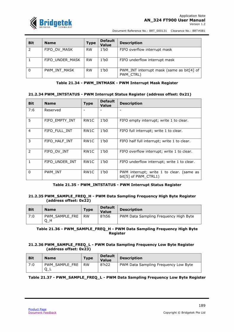
Application Note
AN_324 FT900 User Manual Version 1.2
Document Reference No.: BRT_000131 Clearance No.: BRT#081
189 Product Page Document Feedback Copyright © Bridgetek Pte Ltd
Bit Name Type Default Value
Description
2 FIFO_OV_MASK RW 1’b0 FIFO overflow interrupt mask
1 FIFO_UNDER_MASK RW 1’b0 FIFO underflow interrupt mask
0 PWM_INT_MASK RW 1’b0 PWM_INT interrupt mask (same as bit[4] of PWM_CTRL)
Table 21.34 - PWM_INTMASK - PWM Interrupt Mask Register
21.2.34 PWM_INTSTATUS - PWM Interrupt Status Register (address offset: 0x21)
Bit Name Type Default Value
Description
7:6 Reserved - - -
5 FIFO_EMPTY_INT RW1C 1’b0 FIFO empty interrupt; write 1 to clear.
4 FIFO_FULL_INT RW1C 1’b0 FIFO full interrupt; write 1 to clear.
3 FIFO_HALF_INT RW1C 1’b0 FIFO half full interrupt; write 1 to clear.
2 FIFO_OV_INT RW1C 1’b0 FIFO overflow interrupt; write 1 to clear.
1 FIFO_UNDER_INT RW1C 1’b0 FIFO underflow interrupt; write 1 to clear.
0 PWM_INT RW1C 1’b0 PWM interrupt; write 1 to clear. (same as
bit[5] of PWM_CTRL1)
Table 21.35 - PWM_INTSTATUS - PWM Interrupt Status Register
21.2.35 PWM_SAMPLE_FREQ_H - PWM Data Sampling Frequency High Byte Register
(address offset: 0x22)
Bit Name Type Default
Value Description
7:0 PWM_SAMPLE_FREQ_H
RW 8’h56 PWM Data Sampling Frequency High Byte
Table 21.36 - PWM_SAMPLE_FREQ_H - PWM Data Sampling Frequency High Byte Register
21.2.36 PWM_SAMPLE_FREQ_L - PWM Data Sampling Frequency Low Byte Register
(address offset: 0x23)
Bit Name Type Default
Value Description
7:0 PWM_SAMPLE_FRE
Q_L
RW 8’h22 PWM Data Sampling Frequency Low Byte
Table 21.37 - PWM_SAMPLE_FREQ_L - PWM Data Sampling Frequency Low Byte Register
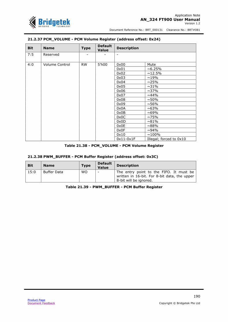
Application Note
AN_324 FT900 User Manual Version 1.2
Document Reference No.: BRT_000131 Clearance No.: BRT#081
190 Product Page Document Feedback Copyright © Bridgetek Pte Ltd
21.2.37 PCM_VOLUME - PCM Volume Register (address offset: 0x24)
Bit Name Type Default Value
Description
7:5 Reserved - - -
4:0 Volume Control RW 5’h00 0x00 Mute
0x01 ~6.25%
0x02 ~12.5%
0x03 ~19%
0x04 ~25%
0x05 ~31%
0x06 ~37%
0x07 ~44%
0x08 ~50%
0x09 ~56%
0x0A ~63%
0x0B ~69%
0x0C ~75%
0x0D ~81%
0x0E ~88%
0x0F ~94%
0x10 ~100%
0x11-0x1F Illegal; forced to 0x10
Table 21.38 - PCM_VOLUME - PCM Volume Register
21.2.38 PWM_BUFFER - PCM Buffer Register (address offset: 0x3C)
Bit Name Type Default Value
Description
15:0 Buffer Data WO - The entry point to the FIFO. It must be written in 16-bit. For 8-bit data, the upper
8-bit will be ignored.
Table 21.39 - PWM_BUFFER - PCM Buffer Register

Application Note
AN_324 FT900 User Manual Version 1.2
Document Reference No.: BRT_000131 Clearance No.: BRT#081
191 Product Page Document Feedback Copyright © Bridgetek Pte Ltd
22 Data Capture Interface
There is an 8-bit parallel interface to collect byte streaming data from a sensor peripheral - e.g. a camera module - in a 2Kbyte internal FIFO. The interface will provide a clock to the peripheral at a speed of 25MHz (max).
22.1 Register Summary
Listed below are the registers with their offset from the base address (0x10360). All registers can only be accessed via Double-Word (32-bit) mode.
Address Offset
Register Default value
References
0x00 DCAP_REG1 – Data Capture Interface Register 1 0x00000FFC Section 22.2.1
0x04 DCAP_REG2 – Data Capture Interface Register 2 0x00000000 Section 22.2.2
0x08 DCAP_REG3 – Data Capture Interface Register 3 0x00000000 Section 22.2.3
0x0C DCAP_REG4 – Data Capture Interface Register 4 0x00000000 Section 22.2.4
Table 22.1 - Overview of Data Capture Interface Registers
22.2 Register Details
22.2.1 DCAP_REG1 – Data Capture Interface Register 1 (address offset: 0x00)
Bit Name Type Default Value
Description
31:16 COUNT RW 16’h0000 Number of bytes to capture after the last trigger event. This must be in multiple of 4 bytes
15:12 TRIG_PAT RW 4’h0
This specifies the data capture trigger position. Data capture starts on the cycle when trigger transitions from 0 to 1
En[1] / VD En[0] / HD Trigger
0 0 TRIG_PAT[0]
0 1 TRIG_PAT[1]
1 0 TRIG_PAT[2]
1 1 TRIG_PAT[3]
11:0 THRESHOLD RW 12’hFFC Specifies the threshold value for the HAS_DATA signal. It must be a multiple of 4 bytes
Table 22.2 - DCAP_REG1 – Data Capture Interface Register 1
22.2.2 DCAP_REG2 – Data Capture Interface Register 2 (address offset: 0x04)
Bit Name Type Default Value
Description
31:12 Reserved - - -

Application Note
AN_324 FT900 User Manual Version 1.2
Document Reference No.: BRT_000131 Clearance No.: BRT#081
192 Product Page Document Feedback Copyright © Bridgetek Pte Ltd
Bit Name Type Default Value
Description
11:0 FULLNESS RO 12’’h000 Specifies the number of bytes that can be safely read from the FIFO. Its value is always a multiple of 4
Table 22.3 - DCAP_REG2 – Data Capture Interface Register 2
22.2.3 DCAP_REG3 – Data Capture Interface Register 3 (address offset: 0x08)
Bit Name Type Default Value
Description
31:0 DATA RO - Next four samples from the FIFO. Reading this will remove the sample from the FIFO. When FULLNESS is 0, the effect is non-deterministic
Table 22.4 - DCAP_REG3 – Data Capture Interface Register 3
22.2.4 DCAP_REG4 – Data Capture Interface Register 4 (address offset: 0x0C)
Bit Name Type Default Value
Description
31:3 Reserved - - -
2 HAS_DATA RO 1’b0 Set when FIFO contains at least THRESHOLD bytes.
1 CLK_SENSE RW 1’b0 1: capture data on clock rising edge
0 INT_ENB RW 1’b0 1: enable interrupt; an interrupt will be generated when HAS_DATA = 1
Table 22.5 - DCAP_REG4 – Data Capture Interface Register 4

Application Note
AN_324 FT900 User Manual Version 1.2
Document Reference No.: BRT_000131 Clearance No.: BRT#081
193 Product Page Document Feedback Copyright © Bridgetek Pte Ltd
23 Flash Controller
There are two ways to access the memory control unit. One is via the CPU I/O interface and the other via the FTDI 1-wire debugger interface. The CPU I/O interface is described here.
From the CPU I/O interface, memory transfer can occur between the Flash and the Program Memory, and between the Flash and the Data Memory. A number of the serial Flash commands are also supported, and the CPU may issue these commands to the Flash.
As this is a shared resource between the debugger interface and CPU I/O interface, the interface must acquire the resource first before performing any of the activities. This is done by reading a test-and-set semaphore. If the interface reads a 0 from the semaphore it can safely assume it has
acquired the resource. Any further read to this semaphore will return a 1 until it is released by the interface that acquired the resource.
If both the debugger and CPU attempt to acquire the resource while it is free at exactly the same time, priority is given to the debugger and the CPU interface will read a 1 instead.
Until the semaphore is acquired, the semaphore is the only register any of the interfaces can read. Once the semaphore is acquired by the interface, the interface will have full access to all the registers in the control unit.
If an interface that does not have the resource writes to the control unit registers they will be ignored while a read from any of the control unit registers will always return 0.
23.1 Register Summary
Listed below are the registers with their offset from the base address (0x10800). All registers can only be accessed via Byte (8-bit) mode.
Address Offset
Register Default value
References
0x00 RSADDR0 – Memory Start Address Register (LSB) 0x00 Section 23.2.1
0x01 RSADDR1 – Memory Start Address Register (Byte 1)
0x00 Section 23.2.2
0x02 RSADDR2 – Memory Start Address Register (MSB) 0x00 Section 23.2.3
0x03 FSADDR0 – Flash Start Address Register (LSB) 0x00 Section 23.2.4
0x04 FSADDR1 – Flash Start Address Register (Byte 1) 0x00 Section 23.2.5
0x05 FSADDR2 – Flash Start Address Register (MSB) 0x00 Section 23.2.6
0x06 BLENGTH0 – Data Byte Length Register (LSB) 0x00 Section 23.2.7
0x07 BLENGTH1 – Data Byte Length Register (Byte 1) 0x00 Section 23.2.8
0x08 BLENGTH2 – Data Byte Length Register (MSB) 0x00 Section 23.2.9
0x09 COMMAND – Command Register 0x00 Section 23.2.10
0x0A Reserved -
0x0B SEMAPHORE – Semaphore Register 0x00 Section 23.2.11
0x0C CONFIG – Configuration Register 0x00 Section 23.2.12
0x0D STATUS – Status Register 0x00 Section 23.2.13
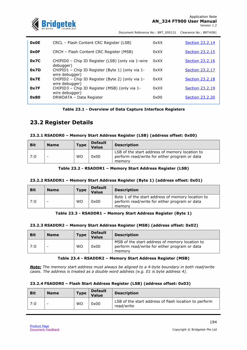
Application Note
AN_324 FT900 User Manual Version 1.2
Document Reference No.: BRT_000131 Clearance No.: BRT#081
194 Product Page Document Feedback Copyright © Bridgetek Pte Ltd
0x0E CRCL – Flash Content CRC Register (LSB) 0xXX Section 23.2.14
0x0F CRCH – Flash Content CRC Register (MSB) 0xXX Section 23.2.15
0x7C CHIPID0 – Chip ID Register (LSB) (only via 1-wire
debugger)
0xXX Section 23.2.16
0x7D CHIPID1 – Chip ID Register (Byte 1) (only via 1-
wire debugger) 0xXX Section 23.2.17
0x7E CHIPID2 – Chip ID Register (Byte 2) (only via 1-
wire debugger) 0xXX Section 23.2.18
0x7F CHIPID3 – Chip ID Register (MSB) (only via 1-
wire debugger)
0xXX Section 23.2.19
0x80 DRWDATA – Data Register 0x00 Section 23.2.20
Table 23.1 - Overview of Data Capture Interface Registers
23.2 Register Details
23.2.1 RSADDR0 – Memory Start Address Register (LSB) (address offset: 0x00)
Bit Name Type Default
Value Description
7:0 - WO 0x00 LSB of the start address of memory location to perform read/write for either program or data memory
Table 23.2 - RSADDR1 – Memory Start Address Register (LSB)
23.2.2 RSADDR1 – Memory Start Address Register (Byte 1) (address offset: 0x01)
Bit Name Type Default Value
Description
7:0 - WO 0x00
Byte 1 of the start address of memory location to
perform read/write for either program or data memory
Table 23.3 - RSADDR1 – Memory Start Address Register (Byte 1)
23.2.3 RSADDR2 – Memory Start Address Register (MSB) (address offset: 0x02)
Bit Name Type Default Value
Description
7:0 - WO 0x00 MSB of the start address of memory location to perform read/write for either program or data memory
Table 23.4 - RSADDR2 – Memory Start Address Register (MSB)
Note: The memory start address must always be aligned to a 4-byte boundary in both read/write cases. The address is treated as a double word address (e.g. 01 is byte address 4).
23.2.4 FSADDR0 – Flash Start Address Register (LSB) (address offset: 0x03)
Bit Name Type Default Value
Description
7:0 - WO 0x00 LSB of the start address of flash location to perform read/write

Application Note
AN_324 FT900 User Manual Version 1.2
Document Reference No.: BRT_000131 Clearance No.: BRT#081
195 Product Page Document Feedback Copyright © Bridgetek Pte Ltd
Table 23.5 - FSADDR0 – Flash Start Address Register (LSB)
23.2.5 FSADDR1 – Flash Start Address Register (Byte 1) (address offset: 0x04)
Bit Name Type Default Value
Description
7:0 - WO 0x00 Byte 1 of the start address of flash location to perform read/write
Table 23.6 - FSADDR1 – Flash Start Address Register (Byte 1)
23.2.6 FSADDR2 – Flash Start Address Register (MSB) (address offset: 0x05)
Bit Name Type Default Value
Description
7:0 - WO 0x00 MSB of the start address of flash location to perform
read/write
Table 23.7 - FSADDR2 – Flash Start Address Register (MSB)
Note: The flash start address must always be aligned to 256-byte boundary in the write case, and can be any value in the read case. The address is treated as a byte address (e.g. 01 is byte address 1).
23.2.7 BLENGTH0 – Data Byte Length Register (LSB) (address offset: 0x06)
Bit Name Type Default
Value Description
7:0 - WO 0x00 LSB of the Byte Length to transfer
Table 23.8 - BLENGTH0 – Data Byte Length Register (LSB) (LSB)
23.2.8 BLENGTH1 – Data Byte Length Register (Byte 1) (address offset: 0x07)
Bit Name Type Default Value
Description
7:0 - WO 0x00 Byte 1 of the Byte Length to transfer
Table 23.9 - BLENGTH1 – Data Byte Length Register (Byte 1)
23.2.9 BLENGTH2 – Data Byte Length Register (MSB) (address offset: 0x08)
Bit Name Type Default Value
Description
7:0 - WO 0x00 MSB of the Byte Length to transfer
Table 23.10 - BLENGTH2 – Data Byte Length Register (MSB)
Note 1: When the flash is the destination (write case), the byte length must be a multiple of 256 bytes (1 page of flash entry). There is no such restriction on byte length if the flash is the source (read case).
Note 2: The registers must be set to (byte length - 1). For example, if the byte length is 256, then BLENGTH0 is set to 255 and BLENGTH1 and BLENGTH2 are set to 0.
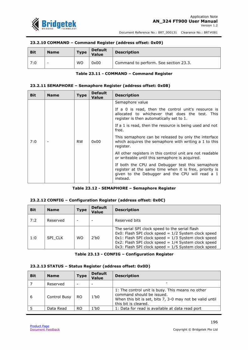
Application Note
AN_324 FT900 User Manual Version 1.2
Document Reference No.: BRT_000131 Clearance No.: BRT#081
196 Product Page Document Feedback Copyright © Bridgetek Pte Ltd
23.2.10 COMMAND – Command Register (address offset: 0x09)
Bit Name Type Default Value
Description
7:0 - WO 0x00 Command to perform. See section 23.3.
Table 23.11 - COMMAND – Command Register
23.2.11 SEMAPHORE – Semaphore Register (address offset: 0x0B)
Bit Name Type Default Value
Description
7:0 - RW 0x00
Semaphore value
If a 0 is read, then the control unit's resource is
allocated to whichever that does the test. This
register is then automatically set to 1.
If a 1 is read, then the resource is being used and not free.
This semaphore can be released by only the interface which acquires the semaphore with writing a 1 to this
register.
All other registers in this control unit are not readable or writeable until this semaphore is acquired.
If both the CPU and Debugger test this semaphore register at the same time when it is free, priority is given to the Debugger and the CPU will read a 1 instead.
Table 23.12 - SEMAPHORE – Semaphore Register
23.2.12 CONFIG – Configuration Register (address offset: 0x0C)
Bit Name Type Default Value
Description
7:2 Reserved - - Reserved bits
1:0 SPI_CLK WO 2’b0
The serial SPI clock speed to the serial flash
0x0: Flash SPI clock speed = 1/2 System clock speed 0x1: Flash SPI clock speed = 1/3 System clock speed 0x2: Flash SPI clock speed = 1/4 System clock speed 0x3: Flash SPI clock speed = 1/5 System clock speed
Table 23.13 - CONFIG – Configuration Register
23.2.13 STATUS – Status Register (address offset: 0x0D)
Bit Name Type Default Value
Description
7 Reserved - - -
6 Control Busy RO 1’b0
1: The control unit is busy. This means no other command should be issued. When this bit is set, bits 7, 3-0 may not be valid until this bit is cleared.
5 Data Read RO 1’b0 1: Data for read is available at data read port
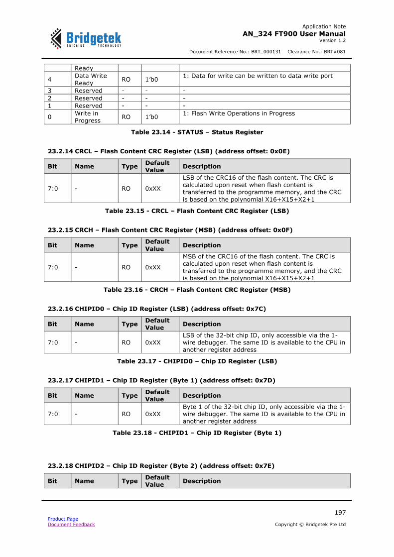
Application Note
AN_324 FT900 User Manual Version 1.2
Document Reference No.: BRT_000131 Clearance No.: BRT#081
197 Product Page Document Feedback Copyright © Bridgetek Pte Ltd
Ready
4 Data Write
Ready RO 1’b0
1: Data for write can be written to data write port
3 Reserved - - -
2 Reserved - - -
1 Reserved - - -
0 Write in Progress
RO 1’b0 1: Flash Write Operations in Progress
Table 23.14 - STATUS – Status Register
23.2.14 CRCL – Flash Content CRC Register (LSB) (address offset: 0x0E)
Bit Name Type Default Value
Description
7:0 - RO 0xXX
LSB of the CRC16 of the flash content. The CRC is
calculated upon reset when flash content is transferred to the programme memory, and the CRC
is based on the polynomial X16+X15+X2+1
Table 23.15 - CRCL – Flash Content CRC Register (LSB)
23.2.15 CRCH – Flash Content CRC Register (MSB) (address offset: 0x0F)
Bit Name Type Default
Value Description
7:0 - RO 0xXX
MSB of the CRC16 of the flash content. The CRC is calculated upon reset when flash content is transferred to the programme memory, and the CRC is based on the polynomial X16+X15+X2+1
Table 23.16 - CRCH – Flash Content CRC Register (MSB)
23.2.16 CHIPID0 – Chip ID Register (LSB) (address offset: 0x7C)
Bit Name Type Default Value
Description
7:0 - RO 0xXX LSB of the 32-bit chip ID, only accessible via the 1-wire debugger. The same ID is available to the CPU in another register address
Table 23.17 - CHIPID0 – Chip ID Register (LSB)
23.2.17 CHIPID1 – Chip ID Register (Byte 1) (address offset: 0x7D)
Bit Name Type Default Value
Description
7:0 - RO 0xXX Byte 1 of the 32-bit chip ID, only accessible via the 1-wire debugger. The same ID is available to the CPU in another register address
Table 23.18 - CHIPID1 – Chip ID Register (Byte 1)
23.2.18 CHIPID2 – Chip ID Register (Byte 2) (address offset: 0x7E)
Bit Name Type Default Value
Description

Application Note
AN_324 FT900 User Manual Version 1.2
Document Reference No.: BRT_000131 Clearance No.: BRT#081
198 Product Page Document Feedback Copyright © Bridgetek Pte Ltd
7:0 - RO 0xXX Byte 2 of the 32-bit chip ID, only accessible via the 1-wire debugger. The same ID is available to the CPU in another register address
Table 23.19 - CHIPID2 – Chip ID Register (Byte 2)
23.2.19 CHIPID3 – Chip ID Register (MSB) (address offset: 0x7F)
Bit Name Type Default Value
Description
7:0 - RO 0xXX MSB of the 32-bit chip ID, only accessible via the 1-wire debugger. The same ID is available to the CPU in another register address
Table 23.20 - CHIPID3 – Chip ID Register (MSB)
23.2.20 DRWDATA – Data Register (address offset: 0x80)
Bit Name Type Default Value
Description
7:0 - RW 0x00
This is the data read or write port used to transfer data in and out of this control unit. Up to 64 addresses may be used.
When bit 4 of STATUS is not set, writing to this port will have no effect.
When bit 5 of STATUS is not set, reading this port will return 0.
Table 23.21 - DRWDATA – Data Register
23.3 Flash Controller Commands
The following commands are supported by the control unit. The command is initiated once the command register is updated. No further command can be entered until the current one is completed. If two successive commands, regardless what they are, are entered while one is on-
going, the current operation will be aborted. The two commands will not be executed either.
The commands can be divided into 2 groups. The first group consists of commands that are supported directly by the serial flash. The second group consists of commands that initiate data transfer between the debugger/CPU interface and flash, debugger/CPU interface and program/data memory, or flash and program/data memory.
The following table lists the first group of commands. If executing any of these commands that
require data input, write the required data to the DRWDATA register.
Command Code Description
CMDWREN 0x06
The Write Enable (WREN) instruction is for setting the Write Enable Latch (WEL) bit. Those
instructions such as PP, SE,
BE, CE, and WRSR, which are intended to change the device content, should be set every time after the WREN instruction sets the WEL bit.
CMDWRDI 0x04 The Write Disable (WRDI) instruction is for
resetting the Write Enable Latch (WEL) bit.
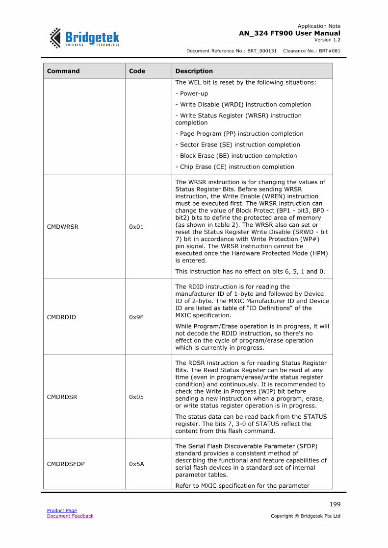
Application Note
AN_324 FT900 User Manual Version 1.2
Document Reference No.: BRT_000131 Clearance No.: BRT#081
199 Product Page Document Feedback Copyright © Bridgetek Pte Ltd
Command Code Description
The WEL bit is reset by the following situations:
- Power-up
- Write Disable (WRDI) instruction completion
- Write Status Register (WRSR) instruction completion
- Page Program (PP) instruction completion
- Sector Erase (SE) instruction completion
- Block Erase (BE) instruction completion
- Chip Erase (CE) instruction completion
CMDWRSR 0x01
The WRSR instruction is for changing the values of Status Register Bits. Before sending WRSR instruction, the Write Enable (WREN) instruction must be executed first. The WRSR instruction can change the value of Block Protect (BP1 - bit3, BP0 -
bit2) bits to define the protected area of memory (as shown in table 2). The WRSR also can set or reset the Status Register Write Disable (SRWD - bit 7) bit in accordance with Write Protection (WP#) pin signal. The WRSR instruction cannot be executed once the Hardware Protected Mode (HPM)
is entered.
This instruction has no effect on bits 6, 5, 1 and 0.
CMDRDID 0x9F
The RDID instruction is for reading the manufacturer ID of 1-byte and followed by Device ID of 2-byte. The MXIC Manufacturer ID and Device
ID are listed as table of "ID Definitions" of the
MXIC specification.
While Program/Erase operation is in progress, it will not decode the RDID instruction, so there's no effect on the cycle of program/erase operation which is currently in progress.
CMDRDSR 0x05
The RDSR instruction is for reading Status Register Bits. The Read Status Register can be read at any time (even in program/erase/write status register condition) and continuously. It is recommended to check the Write in Progress (WIP) bit before sending a new instruction when a program, erase, or write status register operation is in progress.
The status data can be read back from the STATUS register. The bits 7, 3-0 of STATUS reflect the
content from this flash command.
CMDRDSFDP 0x5A
The Serial Flash Discoverable Parameter (SFDP) standard provides a consistent method of describing the functional and feature capabilities of
serial flash devices in a standard set of internal parameter tables.
Refer to MXIC specification for the parameter
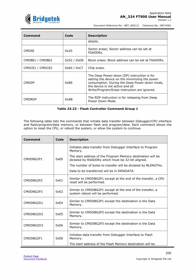
Application Note
AN_324 FT900 User Manual Version 1.2
Document Reference No.: BRT_000131 Clearance No.: BRT#081
200 Product Page Document Feedback Copyright © Bridgetek Pte Ltd
Command Code Description
details.
CMDSE 0x20 Sector erase; Sector address can be set at FSADDRx.
CMDBE1 / CMDBE2 0x52 / 0xD8 Block erase; Block address can be set at FSADDRx.
CMDCE1 / CMDCE2 0x60 / 0xC7 Chip erase.
CMDDP 0xB9
The Deep Power-down (DP) instruction is for setting the device on the minimizing the power consumption. During the Deep Power-down mode, the device is not active and all Write/Program/Erase instruction are ignored.
CMDRDP 0xAB The RDP instruction is for releasing from Deep Power Down Mode.
Table 23.22 - Flash Controller Command Group 1
The following table lists the commands that initiate data transfer between Debugger/CPU interface and flash/program/data memory, or between flash and program/data. Each command allows the option to reset the CPU, or reboot the system, or allow the system to continue.
Command Code Description
CMDDBG2P1 0xE0
Initiates data transfer from Debugger Interface to Program Memory.
The start address of the Program Memory destination will be dictated by RSADDRx which must be 32-bit aligned.
The number of bytes to transfer will be dictated by BLENGTHx.
Data to be transferred will be in DRWDATA.
CMDDBG2P2 0xE1 Similar to CMDDBG2P1 except at the end of the transfer, a CPU reset will be performed.
CMDDBG2P3 0xE2 Similar to CMDDBG2P1 except at the end of the transfer, a
system reboot will be performed.
CMDDBG2D1 0xE4 Similar to CMDDBG2P1 except the destination is the Data Memory.
CMDDBG2D2 0xE5 Similar to CMDDBG2P2 except the destination is the Data
Memory.
CMDDBG2D3 0xE6 Similar to CMDDBG2P3 except the destination is the Data Memory.
CMDDBG2F1 0xE8 Initiates data transfer from Debugger Interface to Flash Memory.
The start address of the Flash Memory destination will be
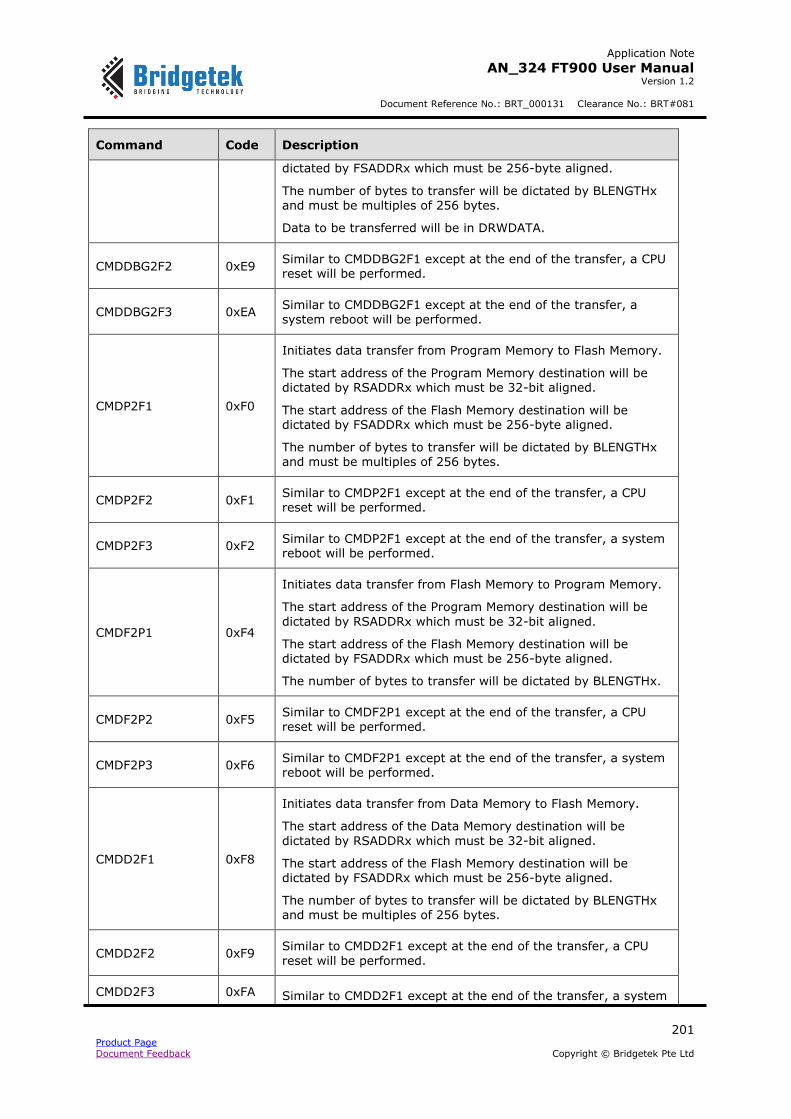
Application Note
AN_324 FT900 User Manual Version 1.2
Document Reference No.: BRT_000131 Clearance No.: BRT#081
201 Product Page Document Feedback Copyright © Bridgetek Pte Ltd
Command Code Description
dictated by FSADDRx which must be 256-byte aligned.
The number of bytes to transfer will be dictated by BLENGTHx and must be multiples of 256 bytes.
Data to be transferred will be in DRWDATA.
CMDDBG2F2 0xE9 Similar to CMDDBG2F1 except at the end of the transfer, a CPU reset will be performed.
CMDDBG2F3 0xEA Similar to CMDDBG2F1 except at the end of the transfer, a system reboot will be performed.
CMDP2F1 0xF0
Initiates data transfer from Program Memory to Flash Memory.
The start address of the Program Memory destination will be dictated by RSADDRx which must be 32-bit aligned.
The start address of the Flash Memory destination will be dictated by FSADDRx which must be 256-byte aligned.
The number of bytes to transfer will be dictated by BLENGTHx and must be multiples of 256 bytes.
CMDP2F2 0xF1 Similar to CMDP2F1 except at the end of the transfer, a CPU reset will be performed.
CMDP2F3 0xF2 Similar to CMDP2F1 except at the end of the transfer, a system reboot will be performed.
CMDF2P1 0xF4
Initiates data transfer from Flash Memory to Program Memory.
The start address of the Program Memory destination will be
dictated by RSADDRx which must be 32-bit aligned.
The start address of the Flash Memory destination will be dictated by FSADDRx which must be 256-byte aligned.
The number of bytes to transfer will be dictated by BLENGTHx.
CMDF2P2 0xF5 Similar to CMDF2P1 except at the end of the transfer, a CPU reset will be performed.
CMDF2P3 0xF6 Similar to CMDF2P1 except at the end of the transfer, a system reboot will be performed.
CMDD2F1 0xF8
Initiates data transfer from Data Memory to Flash Memory.
The start address of the Data Memory destination will be
dictated by RSADDRx which must be 32-bit aligned.
The start address of the Flash Memory destination will be
dictated by FSADDRx which must be 256-byte aligned.
The number of bytes to transfer will be dictated by BLENGTHx and must be multiples of 256 bytes.
CMDD2F2 0xF9 Similar to CMDD2F1 except at the end of the transfer, a CPU
reset will be performed.
CMDD2F3 0xFA Similar to CMDD2F1 except at the end of the transfer, a system

Application Note
AN_324 FT900 User Manual Version 1.2
Document Reference No.: BRT_000131 Clearance No.: BRT#081
202 Product Page Document Feedback Copyright © Bridgetek Pte Ltd
Command Code Description
reboot will be performed.
CMDF2D1 0xFC
Initiates data transfer from Flash Memory to Data Memory.
The start address of the Data Memory destination will be dictated by RSADDRx which must be 32-bit aligned.
The start address of the Flash Memory destination will be dictated by FSADDRx which must be 256-byte aligned.
The number of bytes to transfer will be dictated by BLENGTHx.
CMDF2D2 0xFD Similar to CMDF2D1 except at the end of the transfer, a CPU reset will be performed.
CMDF2D3 0xFE Similar to CMDF2D1 except at the end of the transfer, a system reboot will be performed.
CMDHALT 0xFF This command forces halt immediately to the CPU. The use should be avoided as this cannot be undone. Only a system reset will remove the halt effect.
Table 23.23 - Flash Controller Command Group 2

Application Note
AN_324 FT900 User Manual Version 1.2
Document Reference No.: BRT_000131 Clearance No.: BRT#081
203 Product Page Document Feedback Copyright © Bridgetek Pte Ltd
24 Contact Information
Head Quarters – Singapore Branch Office – Taipei, Taiwan
Bridgetek Pte Ltd 178 Paya Lebar Road, #07-03 Singapore 409030 Tel: +65 6547 4827 Fax: +65 6841 6071
Bridgetek Pte Ltd, Taiwan Branch 2 Floor, No. 516, Sec. 1, Nei Hu Road, Nei Hu District Taipei 114 Taiwan , R.O.C. Tel: +886 (2) 8797 5691 Fax: +886 (2) 8751 9737
E-mail (Sales) [email protected] E-mail (Sales) [email protected] E-mail (Support) [email protected] E-mail (Support) [email protected]
Branch Office - Glasgow, United Kingdom Branch Office – Vietnam
Bridgetek Pte. Ltd. Unit 1, 2 Seaward Place, Centurion Business Park Glasgow G41 1HH United Kingdom
Tel: +44 (0) 141 429 2777 Fax: +44 (0) 141 429 2758
Bridgetek VietNam Company Limited Lutaco Tower Building, 5th Floor, 173A Nguyen Van Troi, Ward 11, Phu Nhuan District,
Ho Chi Minh City, Vietnam Tel : 08 38453222 Fax : 08 38455222
E-mail (Sales) [email protected] E-mail (Sales) [email protected] E-mail (Support) [email protected] E-mail (Support) [email protected]
Web Site
http://brtchip.com/
Distributor and Sales Representatives
Please visit the Sales Network page of the Bridgetek Web site for the contact details of our distributor(s) and sales representative(s) in your country.
System and equipment manufacturers and designers are responsible to ensure that their systems, and any Bridgetek Pte Ltd
(BRT Chip) devices incorporated in their systems, meet all applicable safety, regulatory and system-level performance
requirements. All application-related information in this document (including application descriptions, suggested Bridgetek
devices and other materials) is provided for reference only. While Bridgetek has taken care to assure it is accurate, this
information is subject to customer confirmation, and Bridgetek disclaims all liability for system designs and for any applications
assistance provided by Bridgetek. Use of Bridgetek devices in life support and/or safety applications is entirely at the user’s
risk, and the user agrees to defend, indemnify and hold harmless Bridgetek from any and all damages, claims, suits or expense
resulting from such use. This document is subject to change without notice. No freedom to use patents or other intellectual
property rights is implied by the publication of this document. Neither the whole nor any part of the information contained in, or the product described in this document, may be adapted or reproduced in any material or electronic form without the prior
written consent of the copyright holder. Bridgetek Pte Ltd, 178 Paya Lebar Road, #07-03, Singapore 409030. Singapore
Registered Company Number: 201542387H.
Application Note
AN_324 FT900 User Manual Version 1.2
Document Reference No.: BRT_000131 Clearance No.: BRT#081
204 Product Page Document Feedback Copyright © Bridgetek Pte Ltd
Appendix A – References
Document References
N.A.
Acronyms and Abbreviations
Terms Description
ADC Analogue to Digital Converter
BCD Battery Charger Detection
CAN Controller Area Network
CPRM Content Protection for Recordable Media
CPU Central Processing unit
CRC Cyclic Redundancy Check
DAC Digital to Analogue Converter
FIFO First In First Out
GPIO General Purpose Input Output
I2C Inter-Integrated Circuit
IP Intellectual Property
LSB Least Significant Byte
MAC Media Access Controller
MDC Management Data Clock
MII Media Independent Interface
MMC Multi Media Card
MSB Most Significant Byte
SPI Serial Peripheral Interface
PHY Physical Layer
PWM Pulse Width Modulation
RAM Random Access Memory
SD Secure Digital
Application Note
AN_324 FT900 User Manual Version 1.2
Document Reference No.: BRT_000131 Clearance No.: BRT#081
205 Product Page Document Feedback Copyright © Bridgetek Pte Ltd
Terms Description
STA Used in Ethernet as the “Station Management Controller”
UART Universal Asynchronous Receiver Transmitter
USB Universal Serial Bus
USB-IF USB Implementers Forum
Application Note
AN_324 FT900 User Manual Version 1.2
Document Reference No.: BRT_000131 Clearance No.: BRT#081
206 Product Page Document Feedback Copyright © Bridgetek Pte Ltd
Appendix B – List of Tables & Figures
List of Tables
Table 2.1 - FT900 Program Memory Organization .................................................................. 17
Table 3.1 - Peripheral Availability on FT900 Series Models ...................................................... 19
Table 3.2 - Register Map for FT900 Series ............................................................................ 20
Table 4.1 - Notations used in Register Description ................................................................. 21
Table 5.1 - Overview of General System Registers ................................................................ 23
Table 5.2 - HIPID - Chip ID Register .................................................................................... 24
Table 5.3 - FT900 Series Revision 0001 Configuration ........................................................... 24
Table 5.4 - EFCFG - Chip Configuration Register ................................................................... 25
Table 5.5 - CLKCFG - Clock Configuration Register ................................................................ 25
Table 5.6 - PMCFG - Power Management Register ................................................................. 27
Table 5.7 - PTSTNSET - Test & Set Register ......................................................................... 27
Table 5.8 - PTSTNSETR - Test & Set Shadow Register ........................................................... 27
Table 5.9 - MSC0CFG - Miscellaneous Configuration Register .................................................. 29
Table 5.10 - Pin Configuration Register Description ............................................................... 30
Table 5.11 - Pin 00 – 03 Register ........................................................................................ 30
Table 5.12 - Pin 04 – 07 Register ........................................................................................ 30
Table 5.13 - Pin 08 – 11 Register ........................................................................................ 30
Table 5.14 - Pin 12 – 15 Register ........................................................................................ 30
Table 5.15 - Pin 16 – 19 Register ........................................................................................ 31
Table 5.16 - Pin 20 – 23 Register ........................................................................................ 31
Table 5.17 - Pin 24 – 27 Register ........................................................................................ 31
Table 5.18 - Pin 28 – 31 Register ........................................................................................ 31
Table 5.19 - Pin 32 – 35 Register ........................................................................................ 31
Table 5.20 - Pin 36 – 39 Register ........................................................................................ 32
Table 5.21 - Pin 40 – 43 Register ........................................................................................ 32
Table 5.22 - Pin 44 – 47 Register ........................................................................................ 32
Table 5.23 - Pin 48 – 51 Register ........................................................................................ 32
Table 5.24 - Pin 52 – 55 Register ........................................................................................ 33
Table 5.25 - Pin 56 – 59 Register ........................................................................................ 33
Table 5.26 - Pin 60 – 63 Register ........................................................................................ 34
Table 5.27 - Pin 64 – 66 Register ........................................................................................ 34
Table 5.28 - GPIO Configuration Register Description ............................................................ 35
Table 5.29 - GPIO 00 – 07 Configuration Register ................................................................. 35
Table 5.30 - GPIO 08 – 15 Configuration Register ................................................................. 35
Table 5.31 - GPIO 16 – 23 Configuration Register ................................................................. 35
Application Note
AN_324 FT900 User Manual Version 1.2
Document Reference No.: BRT_000131 Clearance No.: BRT#081
207 Product Page Document Feedback Copyright © Bridgetek Pte Ltd
Table 5.32 - GPIO 24 – 31 Configuration Register ................................................................. 36
Table 5.33 - GPIO 32 – 39 Configuration Register ................................................................. 36
Table 5.34 - GPIO 40 – 47 Configuration Register ................................................................. 36
Table 5.35 - GPIO 48 – 55 Configuration Register ................................................................. 36
Table 5.36 - GPIO 56 – 63 Configuration Register ................................................................. 37
Table 5.37 - GPIO 64 – 66 Configuration Register ................................................................. 37
Table 5.38 - GPIO 00 – 31 Value Register ............................................................................ 37
Table 5.39 - GPIO 32 – 63 Value Register ............................................................................ 37
Table 5.40 - GPIO 64 – 66 Value Register ............................................................................ 37
Table 5.41 - GPIO 00 – 31 Interrupt Enable Register ............................................................. 38
Table 5.42 - GPIO 32 – 63 Interrupt Enable Register ............................................................. 38
Table 5.43 - GPIO 64 – 66 Interrupt Enable Register ............................................................. 38
Table 5.44 - GPIO 00 – 31 Interrupt Pending Register ........................................................... 38
Table 5.45 - GPIO 32 – 63 Interrupt Pending Register ........................................................... 38
Table 5.46 - GPIO 64 – 66 Interrupt Pending Register ........................................................... 39
Table 5.47 - ETH_PHY_CFG - Ethernet PHY Miscellaneous Configuration Register ...................... 39
Table 5.48 - ETH_PHY_ID - Ethernet PHY ID Register ............................................................ 39
Table 5.49 - DAC_ADC_CONF - ADC/DAC Configuration/Status Register .................................. 40
Table 5.50 - DAC_ADC_CNT - ADC/DAC Count Register ......................................................... 41
Table 5.51 - DAC_ADC_DATA - ADC/DAC Data Register ......................................................... 41
Table 6.1 - Interrupt Assignment Table ................................................................................ 43
Table 6.2 - Overview of Interrupt Control Registers ............................................................... 44
Table 6.3 - IRQ00-03 Assignment Register ........................................................................... 44
Table 6.4 - IRQ04-07 Assignment Register ........................................................................... 44
Table 6.5 - IRQ08-11 Assignment Register ........................................................................... 44
Table 6.6 - IRQ12-15 Assignment Register ........................................................................... 45
Table 6.7 - IRQ16-19 Assignment Register ........................................................................... 45
Table 6.8 - IRQ20-23 Assignment Register ........................................................................... 45
Table 6.9 - IRQ24-27 Assignment Register ........................................................................... 45
Table 6.10 - IRQ28-31 Assignment Register ......................................................................... 46
Table 6.11 - IRQ Control Register ....................................................................................... 46
Table 7.1 - EFUSE bits ....................................................................................................... 48
Table 8.1 - Overview of USB Host Controller Registers ........................................................... 50
Table 8.2 - HC Capability Register ....................................................................................... 50
Table 8.3 - HCSPARAMS – HC Structural Parameters ............................................................. 50
Table 8.4 - HCCPARAMS – HC Capability Parameters ............................................................. 51
Table 8.5 - USBCMD – HC USB Command Register ................................................................ 52
Table 8.6 - USBSTS – HC USB Status Register ...................................................................... 53
Table 8.7 - USBINTR – HC USB Interrupt Enable Register ...................................................... 54
Application Note
AN_324 FT900 User Manual Version 1.2
Document Reference No.: BRT_000131 Clearance No.: BRT#081
208 Product Page Document Feedback Copyright © Bridgetek Pte Ltd
Table 8.8 - FRINDEX – HC Frame Index Register ................................................................... 54
Table 8.9 - PERIODICLISTBASE – HC Periodic Frame List Base Address Register ....................... 54
Table 8.10 - ASYNCLISTADDR – HC Current Asynchronous List Address Register ...................... 55
Table 8.11 - PORTSC – HC Port Status and Control Register ................................................... 56
Table 8.12 - EOF Time & Asynchronous Schedule Sleep Timer Register .................................... 58
Table 8.13 - Bus Monitor Control / Status Register ................................................................ 59
Table 8.14 - HPROT – Master Protection Information Setting Register ...................................... 59
Table 8.15 - Vendor Specific IO Control Register ................................................................... 59
Table 8.16 - Vendor Specific Status Register ........................................................................ 59
Table 8.17 - Test Register .................................................................................................. 60
Table 8.18 - HC_RSRV1 - Reserved 1 Register ...................................................................... 60
Table 8.19 - HC_RSRV2 - Reserved 2 Register ...................................................................... 60
Table 9.1 - Overview of USB Peripheral Registers .................................................................. 63
Table 9.2 - DC_ADDRESS_ENABLE – Address Register ........................................................... 63
Table 9.3 - DC_MODE – Mode Register ................................................................................ 63
Table 9.4 - DC_INT_ENABLE – Interrupt Enable Register ....................................................... 64
Table 9.5 - DC_EP_INT_ENABLE – Endpoints Interrupt Enable Register.................................... 64
Table 9.6 - DC_EP0_CONTROL – Endpoint 0 Control Register ................................................. 64
Table 9.7 - DC_EP0_STATUS – Endpoint 0 Status Register ..................................................... 65
Table 9.8 - DC_EP0_BUFFER_LENGTH – Endpoint 0 Buffer Length Register .............................. 65
Table 9.9 - DC_EP0_BUFFER – Endpoint 0 Buffer Register ...................................................... 65
Table 9.10 - DC_EP(x)_CONTROL – Endpoint Control Registers .............................................. 66
Table 9.11 - DC_EP(x)_STATUS – Endpoint Status Registers .................................................. 67
Table 9.12 - DC_EP(x)_BUFFER_LENGTH_LSB – Endpoint Buffer Length LSB Registers .............. 68
Table 9.13 - DC_EP(x)_BUFFER_LENGTH_MSB – Endpoint Buffer Length MSB Registers ............ 68
Table 9.14 - DC_EP(x)_BUFFER – Endpoint Buffer Registers ................................................... 68
Table 9.15 - DC_INT_STATUS – Interrupt Status Register ...................................................... 69
Table 9.16 - DC_EP_INT_STATUS – Endpoints Interrupt Status Register .................................. 69
Table 9.17 - DC_FRAME_NUMBER_LSB – Frame Number LSB Register ..................................... 69
Table 9.18 - DC_FRAME_NUMBER_MSB – Frame Number MSB Register ................................... 69
Table 10.1 - Memory Organization of TX/RX RAM .................................................................. 71
Table 10.2 - Overview of Ethernet Registers ......................................................................... 72
Table 10.3 - ETH_INT_STATUS – Interrupt Status Register .................................................... 73
Table 10.4 - ETH_INT_ENABLE – Interrupt Enable Register .................................................... 73
Table 10.5 - ETH_RX_CNTL – Receive Control Register .......................................................... 74
Table 10.6 - ETH_TX_CNTL – Transmit Control Register ......................................................... 74
Table 10.7 - ETH_DATA_N0 – Data Register (octet n) ............................................................ 74
Table 10.8 - ETH_DATA_N1 – Data Register (octet n+1) ........................................................ 74
Table 10.9 - ETH_DATA_N2 – Data Register (octet n+2) ........................................................ 75
Application Note
AN_324 FT900 User Manual Version 1.2
Document Reference No.: BRT_000131 Clearance No.: BRT#081
209 Product Page Document Feedback Copyright © Bridgetek Pte Ltd
Table 10.10 - ETH_DATA_N3 – Data Register (octet n+3) ...................................................... 75
Table 10.11 - ETH_ADDR_1 – Address Register (octet 1) ....................................................... 75
Table 10.12 - ETH_ADDR_2 – Address Register (octet 2) ....................................................... 75
Table 10.13 - ETH_ADDR_3 – Address Register (octet 3) ....................................................... 75
Table 10.14 - ETH_ADDR_4 – Address Register (octet 4) ....................................................... 75
Table 10.15 - ETH_ADDR_5 – Address Register (octet 5) ....................................................... 75
Table 10.16 - ETH_ADDR_6 – Address Register (octet 6) ....................................................... 76
Table 10.17 - ETH_THRESHOLD – Threshold Register ............................................................ 77
Table 10.18 - ETH_MNG_CNTL – Management Control Register .............................................. 77
Table 10.19 - ETH_MNG_DIV – Management Divider Register ................................................. 77
Table 10.20 - ETH_MNG_ADDR – Management Address Register ............................................ 78
Table 10.21 - ETH_MNG_TX0 – Management Transmit Data 0 Register .................................... 78
Table 10.22 - ETH_MNG_TX1 – Management Transmit Data 1 Register .................................... 78
Table 10.23 - ETH_MNG_RX0 – Management Receive Data 0 Register ..................................... 78
Table 10.24 - ETH_MNG_RX1 – Management Receive Data 1 Register ..................................... 78
Table 10.25 - ETH_NUM_PKT – Number of Packets Register ................................................... 78
Table 10.26 - ETH_TR_REQ – Transmission Request Register ................................................. 79
Table 11.1 - Symbols used in the CAN Frame buffer .............................................................. 80
Table 11.2 - Standard Frames Memory Buffer Layout ............................................................ 81
Table 11.3 - Extended Frames Memory Buffer Layout ............................................................ 81
Table 11.4 - Overview of CAN Registers ............................................................................... 82
Table 11.5 - CAN_MODE – Mode Register ............................................................................. 83
Table 11.6 - CAN_CMD – Command Register ........................................................................ 83
Table 11.7 - CAN_STATUS – Status Register ........................................................................ 84
Table 11.8 - CAN_INT_STATUS – Interrupt Status Register .................................................... 85
Table 11.9 - CAN_INT_ENABLE – Interrupt Enable Register .................................................... 85
Table 11.10 - CAN_RX_MSG – Receive Message Register ....................................................... 86
Table 11.11 - CAN_BUS_TIM_0 – Bus Timing 0 Register ........................................................ 86
Table 11.12 - CAN_BUS_TIM_1 – Bus Timing 1 Register ........................................................ 87
Table 11.13 - CAN_TX_BUF_0 – Transmit Buffer 0 Register .................................................... 87
Table 11.14 - CAN_TX_BUF_1 – Transmit Buffer 1 Register .................................................... 87
Table 11.15 - CAN_TX_BUF_2 – Transmit Buffer 2 Register .................................................... 87
Table 11.16 - CAN_TX_BUF_3 – Transmit Buffer 3 Register .................................................... 88
Table 11.17 - CAN_RX_BUF_0 – Receive Buffer 0 Register ..................................................... 88
Table 11.18 - CAN_RX_BUF_1 – Receive Buffer 1 Register ..................................................... 88
Table 11.19 - CAN_RX_BUF_2 – Receive Buffer 2 Register ..................................................... 88
Table 11.20 - CAN_RX_BUF_3 – Receive Buffer 3 Register ..................................................... 88
Table 11.21- CAN_ACC_CODE_0 – Acceptance Code 0 Register .............................................. 90
Table 11.22 - CAN_ACC_CODE_1 – Acceptance Code 1 Register ............................................. 90
Application Note
AN_324 FT900 User Manual Version 1.2
Document Reference No.: BRT_000131 Clearance No.: BRT#081
210 Product Page Document Feedback Copyright © Bridgetek Pte Ltd
Table 11.23 - CAN_ACC_CODE_2 – Acceptance Code 2 Register ............................................ 90
Table 11.24 - CAN_ACC_CODE_3 – Acceptance Code 3 Register ............................................. 91
Table 11.25 - CAN_ACC_MASK_0 – Acceptance Mask 0 Register ............................................. 91
Table 11.26 - CAN_ACC_MASK_1 – Acceptance Mask 1 Register ............................................. 91
Table 11.27 - CAN_ACC_MASK_2 – Acceptance Mask 2 Register ............................................. 91
Table 11.28 - CAN_ACC_MASK_3 – Acceptance Mask 3 Register ............................................. 92
Table 11.29 - CAN_ERR_CODE – Error Code Capture Register ................................................ 92
Table 11.30 - CAN_RX_ERR_CNTR – Receive Error Counter Register ....................................... 92
Table 11.31 - CAN_TX_ERR_CNTR – Transmit Error Counter Register ...................................... 92
Table 11.32 - CAN_ARB_LOST_CODE – Arbitration Lost Code Capture Register ........................ 93
Table 12.1 - Overview of SD Host Registers ......................................................................... 96
Table 12.2 - 11.2.1 SDH_AUTO_CMD23_ARG2 – Auto CMD23 Argument 2 Register .................. 97
Table 12.3 - 11.2.2 SDH_BLK_SIZE – Block Size Register ...................................................... 97
Table 12.4 - 11.2.3 SDH_BLK_COUNT – Block Count Register ................................................ 97
Table 12.5 - 11.2.4 SDH_ARG_1 – Argument 1 Register ........................................................ 97
Table 12.6 - 11.2.5 SDH_TNSFER_MODE – Transfer Mode Register ......................................... 98
Table 12.7 - 11.2.6 SDH_CMD – Command Register.............................................................. 99
Table 12.8 - 11.2.7 SDH_RESPONSE – Response Register ...................................................... 99
Table 12.9 - 11.2.8 SDH_BUF_DATA – Buffer Data Port Register ............................................. 99
Table 12.10 - 11.2.9 SDH_PRESENT_STATE – Present State Register ..................................... 101
Table 12.11 - SDH_HST_CNTL_1 – Host Control 1 Register ................................................... 102
Table 12.12 - SDH_PWR_CNTL – Power Control Register....................................................... 102
Table 12.13 - SDH_BLK_GAP_CNTL – Block Gap Control Register .......................................... 103
Table 12.14 - SDH_CLK_CNTL – Clock Control Register ........................................................ 103
Table 12.15 - SDH_TIMEOUT_CNTL – Timeout Control Register ............................................. 103
Table 12.16 - SDH_SW_RST – Software Reset Register ........................................................ 104
Table 12.17 - SDH_NRML_INT_STATUS – Normal Interrupt Status Register ............................ 104
Table 12.18 - 11.2.17 SDH_ERR_INT_STATUS – Error Interrupt Status Register ...................... 105
Table 12.19 - SDH_NRML_INT_ENABLE – Normal Interrupt Status Enable Register .................. 106
Table 12.20 - SDH_ERR_INT_ENABLE – Error Interrupt Status Enable Register ........................ 106
Table 12.21 - SDH_NRML_INT_SGNL_ENABLE – Normal Interrupt Signal Enable Register ......... 107
Table 12.22 - SDH_ERR_INT_SGNL_ENABLE – Error Interrupt Signal Enable Register .............. 107
Table 12.23 - SDH_AUTO_CMD12_ERR_STATUS – Auto CMD12 Error Status Register .............. 108
Table 12.24 - SDH_HOST_CNTL_2 – Host Control 2 Register ................................................. 108
Table 12.25 - SDH_CAP_1 – Capabilities Register 1 .............................................................. 109
Table 12.26 - SDH_CAP_2 – Capabilities Register 2 .............................................................. 110
Table 12.27 - SDH_RSRV_1 – Reserved 1 Register ............................................................... 110
Table 12.28 - SDH_RSRV_2 – Reserved 2 Register ............................................................... 110
Application Note
AN_324 FT900 User Manual Version 1.2
Document Reference No.: BRT_000131 Clearance No.: BRT#081
211 Product Page Document Feedback Copyright © Bridgetek Pte Ltd
Table 12.29 - SDH_FORCE_EVT_CMD_ERR_STATUS – Force Event Register for Auto CMD Error Status ............................................................................................................................ 111
Table 12.30 - SDH_FORCE_EVT_ERR_INT_STATUS – Force Event for Error Interrupt Status Register .......................................................................................................................... 111
Table 12.31- SDH_RSRV_3 – Reserved 3 Register ................................................................ 111
Table 12.32 - SDH_RSRV_4 – Reserved 4 Register ............................................................... 112
Table 12.33 - SDH_PRST_INIT – Preset value for initialization ............................................... 112
Table 12.34 - SDH_PRST_DFLT_SPD – Preset value for default speed ..................................... 112
Table 12.35 - SDH_PRST_HIGH_SPD – Preset value for the high speed .................................. 113
Table 12.36 - SDH_PRST_SDR12 – Preset value for SDR12 ................................................... 113
Table 12.37 - SDH_PRST_SDR25 – Preset value for SDR25 ................................................... 114
Table 12.38 - SDH_PRST_SDR50 – Preset value for SDR50 ................................................... 114
Table 12.39 - SDH_PRST_SDR104 – Preset value for SDR104 ............................................... 115
Table 12.40 - SDH_PRST_DDR50 – Preset value for DDR50 .................................................. 115
Table 12.41 - SDH_RSRV_5 – Reserved 5 Register ............................................................... 115
Table 12.42 - SDH_HC_VER – Host Controller Version Register .............................................. 115
Table 12.43 - SDH_VNDR_0 – Vendor-defined 0 Register ...................................................... 116
Table 12.44 - SDH_VNDR_1 – Vendor-defined 1 Register ...................................................... 117
Table 12.45 - SDH_VNDR_2 – Vendor-defined 2 Register ...................................................... 117
Table 12.46 - SDH_VNDR_3 – Vendor-defined 3 Register ...................................................... 117
Table 12.47 - SDH_VNDR_4 – Vendor-defined 4 Register ...................................................... 117
Table 12.48 - SDH_VNDR_5 – Vendor-defined 5 Register ...................................................... 117
Table 12.49 - SDH_VNDR_6 – Vendor-defined 6 Register ...................................................... 118
Table 12.50 - SDH_VNDR_7 – Vendor-defined 7 Register ...................................................... 118
Table 12.51 - SDH_VNDR_8 – Vendor-defined 8 Register ...................................................... 118
Table 12.52 - SDH_VNDR_9 – Vendor-defined 9 Register ...................................................... 118
Table 12.53 - SDH_RSRV_6 – Reserved 6 Register ............................................................... 118
Table 12.54 - SDH_HW_ATTR – Hardware Attributes Register ............................................... 119
Table 12.55 - SDH_CPR_MOD_CNTL – Cipher Mode Control Register ...................................... 120
Table 12.56 - SDH_CPR_MOD_STATUS – Cipher Mode Status Register ................................... 120
Table 12.57 - SDH_CPR_MOD_STATUS_EN – Cipher Mode Status Enable Register ................... 120
Table 12.58 - SDH_CPR_MOD_SIG_EN – Cipher Mode Signal Enable Register .......................... 120
Table 12.59 - SDH_IN_DATA_LSB –Input Data LSB Register ................................................. 121
Table 12.60 - SDH_IN_DATA_MSB –Input Data MSB Register ................................................ 121
Table 12.61 - SDH_IN_KEY_LSB – Input Key LSB Register .................................................... 121
Table 12.62 - SDH_IN_KEY_MSB – Input Key MSB Register .................................................. 121
Table 12.63 - SDH_OUT_DATA_LSB – Output Data LSB Register ........................................... 121
Table 12.64 - SDH_OUT_DATA_MSB – Output Data MSB Register .......................................... 121
Table 12.65 - SDH_SCRT_CONS_DATA – Secret Constant Table Data Port .............................. 122
Table 13.1 - Overview of UART Registers ............................................................................ 125
Application Note
AN_324 FT900 User Manual Version 1.2
Document Reference No.: BRT_000131 Clearance No.: BRT#081
212 Product Page Document Feedback Copyright © Bridgetek Pte Ltd
Table 13.2 - UART mode selection ...................................................................................... 126
Table 13.3 - UART_RBR - Receiver Buffer Register ............................................................... 128
Table 13.4 - UART_THR - Transmitter Holding Register ......................................................... 128
Table 13.5 - UART_DIV_LSB - Divisor LSB Register .............................................................. 128
Table 13.6 - UART_DIV_MSB - Divisor MSB Register ............................................................ 128
Table 13.7 - UART_INT_ENABLE - Interrupt Enable Register .................................................. 129
Table 13.8 - UART_INT_STATUS - Interrupt Status Register .................................................. 129
Table 13.9 - Interrupt Status Register Software Handling ...................................................... 130
Table 13.10 - UART_FCR - FIFO Control Register – 550 mode ................................................ 130
Table 13.11 - UART_RCVR - FIFO Trigger Level – 550 mode .................................................. 131
Table 13.12 - UART_FCR - FIFO Control Register – 650 mode ............................................... 131
Table 13.13 - UART_RCVR - FIFO Trigger Level – 650 mode ................................................. 132
Table 13.14 - XMIT FIFO Trigger Level ............................................................................... 132
Table 13.15 - UART_LCR - Line Control Register .................................................................. 133
Table 13.16 - UART_MCR - Modem Control Register ............................................................. 134
Table 13.17 - UART_LSR - Line Status Register ................................................................... 135
Table 13.18 - UART_MSR - Modem Status Register .............................................................. 136
Table 13.19 - UART_SPR - SPR Register.............................................................................. 136
Table 13.20 - UART_EFR - Enhanced Feature Register .......................................................... 137
Table 13.21 - UART_XON1 - XON1 Register ......................................................................... 137
Table 13.22 - UART_XON2 - XON2 Register ......................................................................... 137
Table 13.23 - UART_XOFF1 - XOFF1 Register ...................................................................... 137
Table 13.24 - UART_XOFF2 - XOFF2 Register ...................................................................... 137
Table 13.25 - UART_ASR - Additional Status Register .......................................................... 138
Table 13.26 - UART_RFL - Receiver FIFO Level Register ....................................................... 138
Table 13.27 - UART_TFL - Transmitter FIFO Level Register ................................................... 138
Table 13.28 - UART_ICR - ICR Register ............................................................................. 139
Table 13.29 - UART_ACR- Additional Control Register .......................................................... 141
Table 13.30 - UART_CPR - Clock Prescaler Register .............................................................. 142
Table 13.31 - UART_TCR - Time Clock Register .................................................................... 142
Table 13.32 - UART_CKS Clock Select Register .................................................................... 142
Table 13.33 - UART_TTL - Transmitter Trigger Level Register ................................................ 143
Table 13.34 - UART_RTL - Receiver Trigger Level Register .................................................... 143
Table 13.35 - UART_FCL - Flow Control Level LSB Register ................................................... 143
Table 13.36 - UART_FCH - Flow Control Level Register MSB .................................................. 144
Table 13.37 - UART_ID1 - Identification 1 Register .............................................................. 144
Table 13.38 - UART_ID2 - Identification 2 Register .............................................................. 144
Table 13.39 UART_ID3 - Identification 3 Register ................................................................ 144
Table 13.40 - UART_REV - Revision Register ....................................................................... 144

Application Note
AN_324 FT900 User Manual Version 1.2
Document Reference No.: BRT_000131 Clearance No.: BRT#081
213 Product Page Document Feedback Copyright © Bridgetek Pte Ltd
Table 13.41 - UART_CSR - Channel Software Reset Register ................................................. 145
Table 13.42 - UART_NMR - Nine Bit Mode Register ............................................................... 145
Table 13.43 - UART_MDM - Modem Disable Mask Register .................................................... 146
Table 13.44 - UART_RFC - Readable FCR Register ................................................................ 146
Table 13.45 - UART_GDS - Good Data Status Register .......................................................... 146
Table 13.46 - UART_RSRV_1 - Reserved 1 Register .............................................................. 146
Table 13.47 - UART_PIDX - Port Index Register ................................................................... 146
Table 13.48 - UART_CKA - Clock Alteration Register ............................................................. 147
Table 14.1 - Timers/Watchdog Operation ............................................................................ 149
Table 14.2 - Overview of Timers/Watchdog Registers ........................................................... 149
Table 14.3 - TIMER_CONTROL_0 - Timers Control Register 0................................................. 149
Table 14.4 - TIMER_CONTROL_1 - Timers Control Register 1................................................. 150
Table 14.5 - TIMER_CONTROL_2 - Timers Control Register 2................................................. 150
Table 14.6 - TIMER_CONTROL_3 - Timers Control Register 3................................................. 150
Table 14.7 - TIMER_CONTROL_4 - Timers Control Register 4................................................. 150
Table 14.8 - TIMER_INT - Timers Interrupt Register ............................................................. 151
Table 14.9 - TIMER_SELECT - Timers A..D Select Register .................................................... 151
Table 14.10 - TIMER_WDG - Watchdog Start Value .............................................................. 151
Table 14.11 - TIMER_WRITE_LS - Timer A..D Start Value 7:0 ................................................ 151
Table 14.12 - TIMER_WRITE_MS - Timer A..D Start Value 15:8 ............................................. 151
Table 14.13 - TIMER_PRESC_LS - Prescaler Start Value 7:0 .................................................. 151
Table 14.14 - TIMER_PRESC_MS - Prescaler Start Value 15:8................................................ 152
Table 14.15 - TIMER_READ_LS - Timer A..D Current Value 7:0 .............................................. 152
Table 14.16 - TIMER_READ_MS - Timer A..D Current Value 15:8 ........................................... 152
Table 15.1 - Oversampling rates supported by FT900 I2S ..................................................... 154
Table 15.2 - FT900 I2S settings ......................................................................................... 154
Table 15.3 - Overview of I2S Registers ............................................................................... 155
Table 15.4 - I2SCR - Configuration Register 1 ..................................................................... 156
Table 15.5 - I2SCR2 - Configuration Register 2 .................................................................... 156
Table 15.6 - I2SIRQEN - Interrupt Enable Register ............................................................... 157
Table 15.7 - I2SIRQPEND - Interrupt Pending Register ......................................................... 157
Table 15.8 - I2SRWDATA - Transmit / Receive Data Register ................................................. 157
Table 15.9 - I2SRXCOUNT - RX Count Register .................................................................... 158
Table 15.10 - I2STXCOUNT - TX Count Register ................................................................... 158
Table 16.1 - Overview of SPI Master Registers ..................................................................... 159
Table 16.2 - SPIM_CNTL – Control Register ......................................................................... 160
Table 16.3 - SPIM_STATUS – Status Register ...................................................................... 161
Table 16.4 - SPIM_DATA – Receiver and Transmitter Data Registers ...................................... 161
Table 16.5 - SPIM_SLV_SEL_CNTL – Slave Select Control Register ......................................... 161

Application Note
AN_324 FT900 User Manual Version 1.2
Document Reference No.: BRT_000131 Clearance No.: BRT#081
214 Product Page Document Feedback Copyright © Bridgetek Pte Ltd
Table 16.6 - SPIM_FIFO_CNTL – FIFO Control Register ........................................................ 162
Table 16.7 - SPIM_TNSFR_FRMT_CNTL – Transfer Format Control Register ............................. 162
Table 16.8 - SPIM_ALT_DATA – Alternative SPI Master Data Register ..................................... 163
Table 16.9 - SPIM_RX_FIFO_COUNT – SPI Master RX FIFO Count Register .............................. 163
Table 17.1 - Overview of SPI Slave Registers ...................................................................... 164
Table 17.2 - SPIS_CNTL – Control Register ......................................................................... 165
Table 17.3 - SPIS_STATUS – Status Register ....................................................................... 165
Table 17.4 - SPIS_DATA – Receiver and Transmitter Data Registers ...................................... 166
Table 17.5 - SPIS_SLV_SEL_CNTL – Slave Select Control Register ......................................... 166
Table 17.6 - SPIS_FIFO_CNTL – FIFO Control Register ........................................................ 166
Table 17.7 - SPIS_TNSFR_FRMT_CNTL – Transfer Format Control Register ............................. 167
Table 17.8 - SPIS_ALT_DATA – Alternative SPI Slave Data Register ....................................... 167
Table 17.9 - SPIS_RX_FIFO_COUNT – SPI Slave RX FIFO Count Register ................................ 167
Table 18.1 - Overview of I2C Master Registers..................................................................... 168
Table 18.2 - I2CM_SLV_ADDR – Slave Address Register ....................................................... 169
Table 18.3 - I2CM_CNTL – Control Register ......................................................................... 169
Table 18.4 - I2CM_STATUS – Status Register ...................................................................... 170
Table 18.5 - I2CM_DATA – Receive / Transmit Data Register ................................................. 170
Table 18.6 - I2CM_TIME_PERIOD – Timer Period Register ..................................................... 170
Table 18.7 - I2CM_HS_TIME_PERIOD – High Speed Timer Period Register .............................. 171
Table 18.8 - I2CM_FIFO_LEN – FIFO Mode Byte Length ........................................................ 171
Table 18.9 - I2CM_FIFO_INT_ENABLE – FIFO Mode Interrupt Enable ...................................... 171
Table 18.10 - I2CM_FIFO_INT_PEND – FIFO Mode Interrupt Pending ...................................... 172
Table 18.11 - I2CM_FIFO_DATA - FIFO Data Register .......................................................... 172
Table 18.12 - I2CM_TRIG - Trigger Register ........................................................................ 172
Table 19.1 - Overview of I2C Master Registers..................................................................... 173
Table 19.2 - I2CS_OWN_ADDR – Own Address Register ....................................................... 174
Table 19.3 - I2CS_CNTL – Control Register ......................................................................... 174
Table 19.4 - I2CS_STATUS – Status Register ...................................................................... 175
Table 19.5 - I2CS_DATA – Receive / Transmit Data Register ................................................. 175
Table 19.6 - I2CS_FIFO_LEN – FIFO Mode Byte Length ......................................................... 175
Table 19.7 - I2CS_FIFO_INT_ENABLE – FIFO Mode Interrupt Enable ...................................... 176
Table 19.8 - I2CS_FIFO_INT_PEND – FIFO Mode Interrupt Pending ........................................ 176
Table 19.9 - I2CS_FIFO_DATA - FIFO Data Register ............................................................. 176
Table 19.10 - I2CS_TRIG - Trigger Register ........................................................................ 176
Table 20.1 - Overview of RTC Registers .............................................................................. 177
Table 20.2 - RTC_CCVR - Current Counter Value Register ..................................................... 177
Table 20.3 - RTC_CMR - Counter Match Register .................................................................. 177
Table 20.4 - RTC_CLR - Counter Load Register .................................................................... 178
Application Note
AN_324 FT900 User Manual Version 1.2
Document Reference No.: BRT_000131 Clearance No.: BRT#081
215 Product Page Document Feedback Copyright © Bridgetek Pte Ltd
Table 20.5 - RTC_CCR - - Counter Control Register .............................................................. 178
Table 20.6 - RTC_STAT - Interrupt Status Register .............................................................. 178
Table 20.7 - RTC_RSTAT - Interrupt Raw Status Register ...................................................... 179
Table 20.8 - RTC_EOI - End of Interrupt Register ................................................................. 179
Table 20.9 - RTC_COMP_VERSION - Component Version Register .......................................... 179
Table 21.1 - Overview of PWM Registers ............................................................................. 181
Table 21.2 - PWM_CTRL0 - PCM Control Register ................................................................. 182
Table 21.3 - PWM_CTRL1 - PWM Control Register ................................................................ 183
Table 21.4 - PWM_PRESCALER - PWM Prescaler Register ...................................................... 183
Table 21.5 - PWM_CNTL - PWM Counter Register (LSB) ........................................................ 183
Table 21.6 - PWM_CNTH - PWM Counter Register (MSB) ....................................................... 183
Table 21.7 - PWM_CMP0L - Comparator 0 Value Register (LSB) ............................................. 183
Table 21.8 - PWM_CMP0H - Comparator 0 Value Register (MSB) ............................................ 183
Table 21.9 - PWM_CMP1L - Comparator 1 Value Register (LSB) ............................................. 184
Table 21.10 - PWM_CMP1H - Comparator 1 Value Register (MSB) .......................................... 184
Table 21.11 - PWM_CMP2L - Comparator 2 Value Register (LSB) ........................................... 184
Table 21.12 - PWM_CMP2H - Comparator 2 Value Register (MSB) .......................................... 184
Table 21.13 - PWM_CMP3L - Comparator 3 Value Register (LSB) ........................................... 184
Table 21.14 - PWM_CMP3H - Comparator 3 Value Register (MSB) .......................................... 184
Table 21.15 - PWM_CMP4L - Comparator 4 Value Register (LSB) ........................................... 185
Table 21.16 - PWM_CMP4H - Comparator 4 Value Register (MSB) .......................................... 185
Table 21.17 - PWM_CMP5L - Comparator 5 Value Register (LSB) ........................................... 185
Table 21.18 - PWM_CMP5H - Comparator 5 Value Register (MSB) .......................................... 185
Table 21.19 - PWM_CMP6L - Comparator 6 Value Register (LSB) ........................................... 185
Table 21.20 - PWM_CMP6H - Comparator 6 Value Register (MSB) .......................................... 186
Table 21.21 - PWM_CMP7L - Comparator 7 Value Register (LSB) ........................................... 186
Table 21.22 - PWM_CMP7H - Comparator 7 Value Register (MSB) .......................................... 186
Table 21.23 - PWM_TOGGLE0 - Channel 0 OUT Toggle Comparator Mask ................................ 186
Table 21.24 - PWM_TOGGLE1 - Channel 1 OUT Toggle Comparator Mask ................................ 186
Table 21.25 - PWM_TOGGLE2 - Channel 2 OUT Toggle Comparator Mask Register ................... 187
Table 21.26 - PWM_TOGGLE3 - Channel 3 OUT Toggle Comparator Mask Register ................... 187
Table 21.27 - PWM_TOGGLE4 - Channel 4 OUT Toggle Comparator Mask Register ................... 187
Table 21.28 - PWM_TOGGLE5 - Channel 5 OUT Toggle Comparator Mask Register ................... 187
Table 21.29 - PWM_TOGGLE6 - Channel 6 OUT Toggle Comparator Mask Register ................... 187
Table 21.30 - PWM_TOGGLE7 - Channel 7 OUT Toggle Comparator Mask Register ................... 188
Table 21.31 - PWM_OUT_CLR_EN - PWM OUT Clear Enable Register ...................................... 188
Table 21.32 - PWM_CTRL_BL_CMP8 - Control Block CMP8 Value Register ................................ 188
Table 21.33 - PWM_INIT - PWM Initialization Register .......................................................... 188
Table 21.34 - PWM_INTMASK - PWM Interrupt Mask Register ................................................ 189
Application Note
AN_324 FT900 User Manual Version 1.2
Document Reference No.: BRT_000131 Clearance No.: BRT#081
216 Product Page Document Feedback Copyright © Bridgetek Pte Ltd
Table 21.35 - PWM_INTSTATUS - PWM Interrupt Status Register ........................................... 189
Table 21.36 - PWM_SAMPLE_FREQ_H - PWM Data Sampling Frequency High Byte Register ....... 189
Table 21.37 - PWM_SAMPLE_FREQ_L - PWM Data Sampling Frequency Low Byte Register ........ 189
Table 21.38 - PCM_VOLUME - PCM Volume Register ............................................................. 190
Table 21.39 - PWM_BUFFER - PCM Buffer Register ............................................................... 190
Table 22.1 - Overview of Data Capture Interface Registers .................................................... 191
Table 22.2 - DCAP_REG1 – Data Capture Interface Register 1 ............................................... 191
Table 22.3 - DCAP_REG2 – Data Capture Interface Register 2 ............................................... 192
Table 22.4 - DCAP_REG3 – Data Capture Interface Register 3 ............................................... 192
Table 22.5 - DCAP_REG4 – Data Capture Interface Register 4 ............................................... 192
Table 23.1 - Overview of Data Capture Interface Registers .................................................... 194
Table 23.2 - RSADDR1 – Memory Start Address Register (LSB) ............................................. 194
Table 23.3 - RSADDR1 – Memory Start Address Register (Byte 1) .......................................... 194
Table 23.4 - RSADDR2 – Memory Start Address Register (MSB)............................................. 194
Table 23.5 - FSADDR0 – Flash Start Address Register (LSB) .................................................. 195
Table 23.6 - FSADDR1 – Flash Start Address Register (Byte 1) .............................................. 195
Table 23.7 - FSADDR2 – Flash Start Address Register (MSB) ................................................. 195
Table 23.8 - BLENGTH0 – Data Byte Length Register (LSB) (LSB) .......................................... 195
Table 23.9 - BLENGTH1 – Data Byte Length Register (Byte 1) ............................................... 195
Table 23.10 - BLENGTH2 – Data Byte Length Register (MSB) ................................................ 195
Table 23.11 - COMMAND – Command Register .................................................................... 196
Table 23.12 - SEMAPHORE – Semaphore Register ................................................................ 196
Table 23.13 - CONFIG – Configuration Register ................................................................... 196
Table 23.14 - STATUS – Status Register ............................................................................. 197
Table 23.15 - CRCL – Flash Content CRC Register (LSB) ....................................................... 197
Table 23.16 - CRCH – Flash Content CRC Register (MSB) ...................................................... 197
Table 23.17 - CHIPID0 – Chip ID Register (LSB) .................................................................. 197
Table 23.18 - CHIPID1 – Chip ID Register (Byte 1) .............................................................. 197
Table 23.19 - CHIPID2 – Chip ID Register (Byte 2) .............................................................. 198
Table 23.20 - CHIPID3 – Chip ID Register (MSB) ................................................................. 198
Table 23.21 - DRWDATA – Data Register ............................................................................ 198
Table 23.22 - Flash Controller Command Group 1 ................................................................ 200
Table 23.23 - Flash Controller Command Group 2 ................................................................ 202
List of Figures
Figure 2.1 - FT900 System Architecture ............................................................................... 17
Figure 2.2 - FT900 Boot Control .......................................................................................... 18
Figure 2.3 - FT900 Debugging Support ................................................................................ 18
Figure 11.1 - CAN Acceptance Filter .................................................................................... 89
Application Note
AN_324 FT900 User Manual Version 1.2
Document Reference No.: BRT_000131 Clearance No.: BRT#081
217 Product Page Document Feedback Copyright © Bridgetek Pte Ltd
Figure 13.1 - ICR registers write access .............................................................................. 139
Figure 13.2 - ICR registers read access ............................................................................... 140
Application Note
AN_324 FT900 User Manual Version 1.2
Document Reference No.: BRT_000131 Clearance No.: BRT#081
218 Product Page Document Feedback Copyright © Bridgetek Pte Ltd
Appendix C – Revision History
Document Title: AN_324 FT900 User Manual
Document Reference No.: BRT_000131
Clearance No.: BRT#081
Product Page: http://brtchip.com/product/
Document Feedback: Send Feedback
Revision Changes Date
1.0 Initial Release 2014-11-07
1.1 Revised Release 2015-10-12
1.2 Migrated from FTDI to Bridgetek 2017-03-30