Future Technology Devices International Ltd DS · PDF fileCopyright © 2013 Future...
27
Copyright © 2013 Future Technology Devices International Limited 1 DS_FT312D USB ANDROID HOST IC Datasheet Version 1.1 Document No.: FT_000816 Clearance No.: FTDI# 331 Future Technology Devices International Ltd. DS_FT312D (USB Android Host IC) The FT312D is a USB 2.0 Full Speed host IC specifically targeted at providing access to peripheral hardware from an Android platform with a USB device port. The device will bridge the USB port to a UART interface via the Android Open Accessory protocol and has the following advanced features: Single chip USB to UART interface. Entire USB protocol handled on the chip. No USB specific firmware programming required. Supports USB bulk transfer mode Basic UART interface with RXD, TXD, RTS#, CTS# pins. TX_ACTIVE signal for controlling transceivers on RS485 interfaces. UART RX buffer size is 5512 bytes UART TX buffer size is 256 bytes USB_ERROR indicator pin Suitable for use on any Android platform supporting Android Open Accessory Mode (Typically 3.1 onwards, however some platforms may port Open Accessory Mode to version 2.3.4) 12MHz oscillator using external crystal. Integrated power-on-reset circuit. +3V3Single Supply Operation with 5V tolerant inputs. USB 2.0 Full Speed compatible. Extended operating temperature range; -40⁰C to 85⁰C. Available in compact Pb-free 32 Pin LQFP and QFN packages (both RoHS compliant). Neither the whole nor any part of the information contained in, or the product described in this manual, may be adapted or reproduced in any material or electronic form without the prior written consent of the copyright holder. This product and its documentation are supplied on an as-is basis and no warranty as to their suitability for any particular purpose is either made or implied. Future Technology Devices International Ltd will not accept any claim for damages howsoever arising as a result of use or failure of this product. Your statutory rights are not affected. This product or any variant of it is not intended for use in any medical appliance, device or system in which the failure of the product might reasonably be expected to result in personal injury. This document provides preliminary information that may be subject to change without notice. No freedom to use patents or other intellectual property rights is implied by the publication of this document. Future Technology Devices International Ltd, Unit 1, 2 Seaward Place, Centurion Business Park, Glasgow G41 1HH United Kingdom. Scotland Registered Company Number: SC136640
-
Upload
nguyenphuc -
Category
Documents
-
view
219 -
download
1
Transcript of Future Technology Devices International Ltd DS · PDF fileCopyright © 2013 Future...

Copyright © 2013 Future Technology Devices International Limited 1
DS_FT312D USB ANDROID HOST IC Datasheet
Version 1.1 Document No.: FT_000816 Clearance No.: FTDI# 331
Future Technology Devices International Ltd.
DS_FT312D
(USB Android Host IC)
The FT312D is a USB 2.0 Full Speed host IC specifically targeted at
providing access to peripheral hardware from an Android platform
with a USB device port. The device will bridge the USB port to a UART
interface via the Android Open Accessory protocol and has the
following advanced features:
Single chip USB to UART interface.
Entire USB protocol handled on the chip. No USB specific firmware programming required.
Supports USB bulk transfer mode
Basic UART interface with RXD, TXD, RTS#,
CTS# pins.
TX_ACTIVE signal for controlling transceivers
on RS485 interfaces.
UART RX buffer size is 5512 bytes
UART TX buffer size is 256 bytes
USB_ERROR indicator pin
Suitable for use on any Android platform supporting Android Open Accessory Mode (Typically 3.1 onwards, however some
platforms may port Open Accessory Mode to version 2.3.4)
12MHz oscillator using external crystal.
Integrated power-on-reset circuit.
+3V3Single Supply Operation with 5V tolerant inputs.
USB 2.0 Full Speed compatible.
Extended operating temperature range; -40⁰C
to 85⁰C.
Available in compact Pb-free 32 Pin LQFP and QFN packages (both RoHS compliant).
Neither the whole nor any part of the information contained in, or the product described in this manual, may be adapted or reproduced in any material or electronic form without the prior written consent of the copyright holder. This product and its documentation are
supplied on an as-is basis and no warranty as to their suitability for any particular purpose is either made or implied. Future Technology
Devices International Ltd will not accept any claim for damages howsoever arising as a result of use or failure of this product. Your
statutory rights are not affected. This product or any variant of it is not intended for use in any medical appliance, device or system in
which the failure of the product might reasonably be expected to result in personal injury. This document provides preliminary
information that may be subject to change without notice. No freedom to use patents or other intellectual property rights is implied by
the publication of this document. Future Technology Devices International Ltd, Unit 1, 2 Seaward Place, Centurion Business Park, Glasgow
G41 1HH United Kingdom. Scotland Registered Company Number: SC136640

Copyright © 2013 Future Technology Devices International Limited 2
DS_FT312D USB ANDROID HOST IC Datasheet
Version 1.1 Document No.: FT_000816 Clearance No.: FTDI# 331
1 Typical Applications
Connecting Android phones to USB accessories
Connecting Android tablets to USB accessories
Controlling instrumentation from Android devices.
Home automation via Android devices
Data logging from USB accessories
Connecting serial printing devices to Android devices
1.1 Part Numbers
Part Number Package
FT312D-32Q1C-x 32 Pin QFN
FT312D-32L1C-x 32 Pin LQFP
Note: Packing codes for x is:
- R: Taped and Reel, QFN 3,000pcs per reel, LQFP 1500 pcs per reel.
- (no suffix): Tray packing, 260pcs per tray QFN, 250 pcs per tray LQFP
For example: FT312D-32Q1C-R is 3,000pcs QFN taped and reel packing
1.2 USB Compliant
At the time of writing this datasheet, the FT312Dhad not completed the USB Compliancy Test.

Copyright © 2013 Future Technology Devices International Limited 3
DS_FT312D USB ANDROID HOST IC Datasheet
Version 1.1 Document No.: FT_000816 Clearance No.: FTDI# 331
2 FT312D Block Diagram
USB
TransceiverUSB Host Buffer UART
USBDP
USBDM
TXD
RXD
RTS#
CTS#
TX_ACTIVE
USB_ERROR#
Figure 2.1FT312D Block Diagram
For a description of the function please refer to Section 4.
Copyright © 2013 Future Technology Devices International Limited 4
DS_FT312D USB ANDROID HOST IC Datasheet
Version 1.1 Document No.: FT_000816 Clearance No.: FTDI# 331
Table of Contents
1 Typical Applications ...................................................................... 2
1.1 Part Numbers ..................................................................................... 2
1.2 USB Compliant .................................................................................... 2
2 FT312D Block Diagram ................................................................. 3
3 Device Pin Out and Signal Description .......................................... 6
3.1 Package Symbol.................................................................................. 6
3.1.1 Package PinOut Description ........................................................................................... 6
4 Function Description..................................................................... 8
4.1 Key Features ....................................................................................... 8
4.2 Functional Block Descriptions ............................................................. 8
4.2.1 UART Interface Module ................................................................................................. 8
4.2.2 Buffers ....................................................................................................................... 8
4.2.3 USB Host .................................................................................................................... 8
4.2.4 USB Transceivers ......................................................................................................... 8
4.3 Default Descriptor Strings .................................................................. 8
5 UART Interface ........................................................................... 10
6 USB Error Detection .................................................................... 12
7 Absolute Maximum Ratings ........................................................ 13
7.1 DC Characteristics .............................................................................14
7.2 ESD and Latch-up Specifications ........................................................15
8 Application Examples ................................................................. 16
8.1 USB to UARTConverter .......................................................................16
8.2 USB to RS232 Converter ....................................................................17
9 Package Parameters ................................................................... 18
9.1 FT312D Package Markings .................................................................18
9.1.1 QFN-32 .................................................................................................................... 18
9.1.2 LQFP-32 ................................................................................................................... 19
9.2 FT312DPackage Dimensions ..............................................................20
9.2.1 QFN-32 Package Dimensions ....................................................................................... 20
9.2.2 LQFP-32 Package Dimensions ...................................................................................... 21
9.3 Solder Reflow Profile .........................................................................22
10 Contact Information ................................................................... 24
Appendix A – References ............................................................................25
Appendix B - List of Figures and Tables ......................................................26
Appendix C - Revision History .....................................................................27

Copyright © 2013 Future Technology Devices International Limited 5
DS_FT312D USB ANDROID HOST IC Datasheet
Version 1.1 Document No.: FT_000816 Clearance No.: FTDI# 331

Copyright © 2013 Future Technology Devices International Limited 6
DS_FT312D USB ANDROID HOST IC Datasheet
Version 1.1 Document No.: FT_000816 Clearance No.: FTDI# 331
3 Device Pin Out and Signal Description
3.1 Package Symbol
17
18
19
20
21
22
23
24
USBDP
FT312D
QFN 32
USBDM
GND
NC
NC
VCCIO
TXD
RXD
RT
S#
25
26
27
28
29
30
31
32
CT
S#
GN
D
VC
CIO
TX
_A
CT
IVE
NC
NC
US
B_
ER
RO
R#
GN
D3
3
1
2
3
4
5
6
7
8
910
11
12
13
14
15
16
TEST1
VREGOUT
GND
XTOUT
XTIN
AVCC
VCC
GND
GN
D
GN
D
GN
D
VC
CIO NC
TE
ST
0
RE
SE
T#
TE
ST
2
Figure 3.1QFN Schematic Symbol
NOTE: The pinout is the same for the QFN and LQFP packages.
NOTE: Pin 33 on the symbol is the copper pad in the centre of the QFN package
3.1.1 Package PinOut Description
Note: # denotes an active low signal.
Pin No. Name Type Description
2 VCC POWER Input
3V3 supply to IC internal 1V8 regulator
3 AVCC POWER
Input 1V8 supply to IC core
13, 22, 28 VCCIO POWER
Input 3V3 supply for the IO cells
7 VREGOUT POWER Output
1V8 output. May be used as input source for pin 3.
1,6,14,15,16,19,27 GND POWER
Input 0V Ground input.
Table 3.1 Power and Ground

Copyright © 2013 Future Technology Devices International Limited 7
DS_FT312D USB ANDROID HOST IC Datasheet
Version 1.1 Document No.: FT_000816 Clearance No.: FTDI# 331
Pin No. Name Type Description
4 XTIN INPUT Input to 12MHz Oscillator Cell. Connect 12MHz crystal across pins 4 and 5.
5 XTOUT OUTPUT Output from 12MHz Oscillator Cell. Connect 12MHz
crystal across pins 4 and 5.
8 TEST1 INPUT For internal use. Pull to GND
9 TEST2 INPUT For factory use. Pull to 3V3.
10 RESET# INPUT Reset input (active low).
11 TEST0 OUTPUT Leave unterminated.
12 NC - No connect pins. Leave unterminated.
17 USBDP INPUT/OUTPUT USB Data Signal Plus.
18 USBDM INPUT/OUTPUT USB Data Signal Minus.
20 NC - No connect pins. Leave unterminated.
21 NC - No connect pins. Leave unterminated.
23 TXD OUTPUT Transmit asynchronous data output
24 RXD INPUT Receive asynchronous data input
25 RTS# OUTPUT Request to send control output
26 CTS# INPUT Clear to send control input
29 TX_ACTIVE OUTPUT UART active signal (typically used with RS485)
30 NC - No connect pins. Leave un-terminated
31 NC - No connect pins. Leave un-terminated
32 USB_ERROR# OUTPUT Output signal to indicate a problem with the USB connection
Table 3.2 Function pins

Copyright © 2013 Future Technology Devices International Limited 8
DS_FT312D USB ANDROID HOST IC Datasheet
Version 1.1 Document No.: FT_000816 Clearance No.: FTDI# 331
4 Function Description
The FT312D is FTDI’s second dedicated Android Open Accessory Mode integrated circuit device or Android Host. The FT312D USB host port is dedicated to support of the Android Open Accessory class and will bridge data between this port and the UART interface.
4.1 Key Features
Easy to use Android Open Accessory IC translating the Device port of the Android device into UART capabilities
4.2 Functional Block Descriptions The following paragraphs describe each function within FT312D. Please refer to the block diagram shown inFigure 2.1.
4.2.1 UART Interface Module
The FT312DUART module controls the UART interface providing basic RXD, TXD signalling with RTS#/CTS# hardware flow control. An additional TX_Active signal is supplied to control external RS485 transceivers for users wishing to create a USB to RS485 bridge. The UART supports baud rates from 300
baud to 921600 baud. A full description of the UART module is provided in Section 5.
4.2.2 Buffers
The FT312D provides internal buffering between the USB port and the UART port of the IC for smooth data streaming.
The Android device can send NAK’s to the USB OUT token sent from the FT312D. This can happen when the UART application on the Android is running in the background or multiple applications are launched in
the Android device. When the UART application on the Android device is not accepting data, the data will be buffered in the UART RX buffer in FT312D. The UART RX buffer size is 5512 bytes.
The UART_TX buffer which stores data from the USB port, heading for the UART is 256 bytes.
4.2.3 USB Host
The USB Host block handles the parallel-to-serial and serial-to-parallel conversion of the USB physical layer. This includes bit stuffing, CRC generation.
4.2.4 USB Transceivers
USB transceiver cells provide the physical USB device interface supporting USB 1.1 and USB 2.0
standards. Low-speed and full-speed USB data rates are supported. The output driver provides 3V3 level slew rate control signalling, whilst a differential receiver and two single ended receivers provide USB DATA IN, SE0 and USB Reset condition detection. These cells also include integrated internal pull-down resistors as required for host mode.
4.3 Default Descriptor Strings
When the USB port is connected to the Android USB port, the Android platform will determine which application to load based on the strings read from the FT312D. These strings are configurable with a Windows utility: FT312D_Cofiguration available for download from the FTDI website.
http://www.ftdichip.com
Please refer to the application note AN_236 User Guide for FT312D Configuration to change the default string values.

Copyright © 2013 Future Technology Devices International Limited 9
DS_FT312D USB ANDROID HOST IC Datasheet
Version 1.1 Document No.: FT_000816 Clearance No.: FTDI# 331
Default values for the strings are set in the device as per Table 4.1
Descriptor String Default Value
Manufacturer FTDI
Model Android Accessory FT312D
Version 1.0
Serial FTDI FT312D
URL http://www.ftdichip.com/Android.htm
Description FTDI Android Accessory FT312D
Table 4.1Default Descriptor Strings

Copyright © 2013 Future Technology Devices International Limited 10
DS_FT312D USB ANDROID HOST IC Datasheet
Version 1.1 Document No.: FT_000816 Clearance No.: FTDI# 331
5 UART Interface
The interface implements a standard asynchronous serial UART port with flow control, for example RS232/422/485. The UART can support baud rates from 300 to 921600 with RTS/CTS flow control. The UART can support baud rates from 300 to 115200 with no flow control.
Data transfer uses NRZ (Non-Return to Zero) data format consisting of 1 start bit, 7 or 8 data bits, an
optional parity bit, and one or two stop bits. When transmitting the data bits, the least significant bit is
transmitted first. Transmit and receive waveforms are illustrated in Figure 5-1 and Figure 5-2:
Figure 5-1 UART Receive Waveform
Figure 5-2 UART Transmit Waveform
Baud rate (default =9600 baud), flow control settings (default = None), number of data bits (default=8), parity (default is no parity) and number of stop bits (default=1) are all configurable from the Android application. Please refer to ftdichip document number FT_000532 for further details.
http://www.ftdichip.com
TX_ACTIVE is transmit enable, this output may be used in RS485 designs to enable the line driver for transmit mode.
UART RX buffer size is 5512 bytes and UART TX buffer size is 256 bytes.
Note: UART software flow control with XON/XOFF is not supported
UART hardware flow control with DTR/DSR is not supported
Note:
The FT312D has to enumerate the Android device before receiving data from the UART device.
This can be implemented by disconnecting the UART TXD signal of external UART device connected to the FT312D RXD signal until after the FT312D has established the USB link with Android device.
The connection sequence should be:
1. Connect FT312D to Android and complete enumeration.
2. Connect the TXD of UART device to FT312D’s RXD then start to receive data.
There are two methods to implement this function:
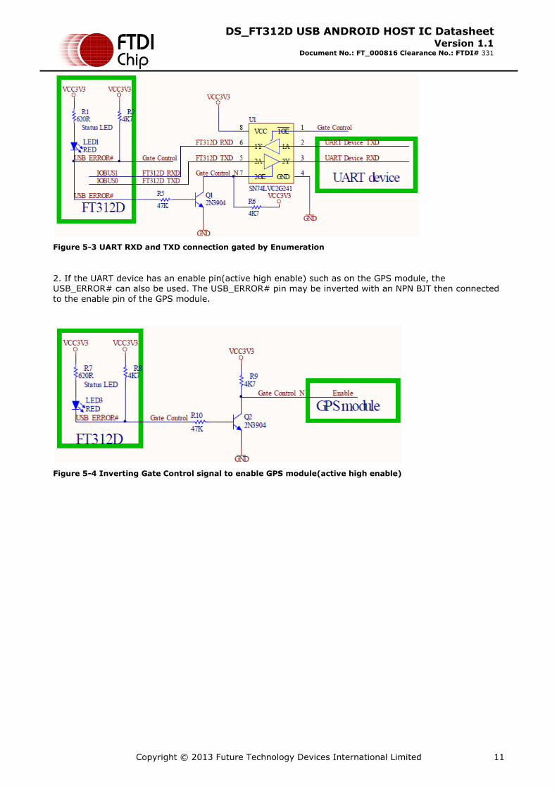
1.When FT312D connects to the Android device and enumeration is completed, the USB_ERROR# will become Logic 0 (default Logic 1). This signal can be used to control the TTL gate (74LVC2G241, 74LVC1G125 or others) ON/OFF such that the TXD/RXD lines are connected/disconnected.
Copyright © 2013 Future Technology Devices International Limited 11
DS_FT312D USB ANDROID HOST IC Datasheet
Version 1.1 Document No.: FT_000816 Clearance No.: FTDI# 331
Figure 5-3 UART RXD and TXD connection gated by Enumeration
2. If the UART device has an enable pin(active high enable) such as on the GPS module, the USB_ERROR# can also be used. The USB_ERROR# pin may be inverted with an NPN BJT then connected to the enable pin of the GPS module.
Figure 5-4 Inverting Gate Control signal to enable GPS module(active high enable)

Copyright © 2013 Future Technology Devices International Limited 12
DS_FT312D USB ANDROID HOST IC Datasheet
Version 1.1 Document No.: FT_000816 Clearance No.: FTDI# 331
6 USB Error Detection
Pin 32 of the device is provided to indicate a problem has occurred with the USB connection. The errors are USB device not supported, USB hub not supported and USB device not responding. USB device not supported would occur if the USB port was connected to a non-Android class device port. e.g. The FT312D is not designed to host memory sticks or printers etc. USB hub not supported would be reported
if FT312D is connected to a USB hub. USB device not responding would occur if the USB device connected to the FT312D host port did not respond and the enumeration failed. The signal states are as follows:
Pin state Definition
Logic 0 Device connected to USB and functional
Logic 1 Device not connected
One 50ms logic 0 pulse Device not responding. This pulse occurs at plug-in
and then the signal returns to logic 1. This then repeats every second.
Two 50ms logic 0 pulses Device not supported. These pulses occur at plug-in and then the signal returns to logic 1. This then repeats every second.
Three 50ms logic 0 pulses Hub not supported. These pulses occur at plug-in
and then the signal returns to logic 1. This then repeats every second.
Table 6.1 Error Detection

Copyright © 2013 Future Technology Devices International Limited 13
DS_FT312D USB ANDROID HOST IC Datasheet
Version 1.1 Document No.: FT_000816 Clearance No.: FTDI# 331
7 Absolute Maximum Ratings
The absolute maximum ratings for FT312D are shown in Table 7.1. These are in accordance with the Absolute Maximum Rating System (IEC 60134). Exceeding these may cause permanent damage to the device.
Parameter Value Unit
Storage Temperature -65°C to 150°C Degrees C
Floor Life (Out of Bag) At Factory Ambient
( 30°C / 60% Relative Humidity)
168 Hours
(IPC/JEDEC J-STD-033A MSL Level 3
Compliant)*
Hours
Ambient Temperature (Power Applied) -40°C to 85°C Degrees
C.
Vcc Supply Voltage 0 to +3.63 V
VCCIO 0 to +3.63 V
AVCC 0 to + 1.98 V
DC Input Voltage - USBDP and USBDM -0.5 to +(Vcc +0.5) V
DC Input Voltage - High Impedance
Bidirectional -0.5 to +5.00 V
DC Input Voltage - All other Inputs -0.5 to +(Vcc +0.5) V
DC Output Current - Outputs 4 mA
DC Output Current - Low Impedance
Bidirectional 4 mA
Table 7.1 Absolute Maximum Ratings
* If devices are stored out of the packaging beyond this time limit the devices should be baked before use. The devices should be ramped up to a temperature of 125°C and baked for up to 17 hours.

Copyright © 2013 Future Technology Devices International Limited 14
DS_FT312D USB ANDROID HOST IC Datasheet
Version 1.1 Document No.: FT_000816 Clearance No.: FTDI# 331
7.1 DC Characteristics
DC Characteristics (Ambient Temperature -40˚C to +125˚C)
Parameter Description Minimum Typical Maximum Units Conditions
Vcc1 VCC Operating Supply
Voltage 2.97 3.3 3.63 V
Vcc2 VCCIO Operating Supply
Voltage 2.97 3.3 3.63 V
AVCC VCC_PLL Operating
Supply Voltage 1.62 1.8 1.98 V
Icc1
Operating Supply Current
48MHz
25 mA Normal
Operation
Icc2 Operating Supply Current 128 µA USB Suspend
Table 7.2Operating Voltage and Current
Parameter Description Minimum Typical Maximum Units Conditions
Voh Output Voltage High 2.4 V I source = 8mA
Vol Output Voltage Low 0.4 V I sink = 8mA
Vin Input Switching
Threshold 1.5 V
Table 7.3I/O Pin Characteristics
Parameter Description Minimum Typical Maximum Units Conditions
UVoh I/O Pins Static Output
( High) 2.8 V
UVol I/O Pins Static Output
( Low ) 0.3 V
UVse Single Ended Rx
Threshold 0.8 2.0 V
UCom Differential Common
Mode 0.8 2.5 V

Copyright © 2013 Future Technology Devices International Limited 15
DS_FT312D USB ANDROID HOST IC Datasheet
Version 1.1 Document No.: FT_000816 Clearance No.: FTDI# 331
Parameter Description Minimum Typical Maximum Units Conditions
UVdif Differential Input
Sensitivity 0.2 V
UDrvZ Driver Output
Impedance 3 6 9 Ohms
Table 7.4USB I/O Pin (USBDP, USBDM) Characteristics
Parameter Description Minimum Typical Maximum Units Conditions
VCCK
Power supply of internal
core cells and I/O to core
interface
1.62 1.8 1.98 V 1.8V power
supply
VCC18IO Power supply of 1.8V
OSC pad 1.62 1.8 1.98 V
1.8V power
supply
TJ
Operating junction
temperature -40 25 125 °C
Iin Input leakage current -10 ±1 10 µA Iin= VCC18IO or
0V
Ioz Tri-state output leakage
current -10 ±1 10 µA
Table 7.5Crystal Oscillator 1.8 Volts DC Characteristics
7.2 ESD and Latch-up Specifications
Description Specification
Human Body Mode (HBM) ± 2000V
Machine mode (MM) ± 200V
Charged Device Mode (CDM) ± 500V
Latch-up > ± 200mA
Table 7.6 ESD and Latch-up Specifications

Copyright © 2013 Future Technology Devices International Limited 16
DS_FT312D USB ANDROID HOST IC Datasheet
Version 1.1 Document No.: FT_000816 Clearance No.: FTDI# 331
8 Application Examples
The following sections illustrate possible applications of the FT312D.
8.1 USB to UARTConverter
FT312D
1
2
3
4
5
SHIELD
Ferrite
Bead
GND
GND
3V3
GND
VCCIO
VREGOUT
USBDM
USBDP
AVCC
GN
D
RESET#
100nF
100nF
4.7uF+
TX_ACTIVE
5V Power to USB
VCC
3V3
REGULATOR
5V
27R
27R
100nF
3V3
TXD
RXD
RTS#
CTS#
USB_ERROR
GND
47pF47pF
MCU/FPGA
UART_TXD
UART_RXD
UART_RTS#
UART_CTS#
UART_TX_ACTIVE
620R
3V3
LED
Figure 8.1Application Example showing USB to UART Converter
The UART signals are at 3V3 level and may be used to drive directly into a FPGA or MCU with a 3V3 interface, or could be level shifted with an RS232, RS422 or RS485 transceiver. The TX_ACTIVE signal is used mostly with RS485 transceivers to enable the Transmit line drivers.
The unused pins may be left unterminated.

Copyright © 2013 Future Technology Devices International Limited 17
DS_FT312D USB ANDROID HOST IC Datasheet
Version 1.1 Document No.: FT_000816 Clearance No.: FTDI# 331
8.2 USB to RS232 Converter
FT312D
1
2
3
4
5
SHIELD
Ferrite
Bead
GND
GND
3V3
GND
VCCIO
VREGOUT
USBDM
USBDP
AVCC
GN
D
RESET#
100nF
100nF
4.7uF+
TX_ACTIVE
5V Power to USB
VCC
3V3
REGULATOR
5V
27R
27R
100nF
3V3
TXD
RXD
RTS#
CTS#
USB_ERROR
GND
47pF47pF
UART_TXD
UART_RXD
UART_RTS#
UART_CTS#
RS232
LEVEL
CONVERTER
TXD
RXD
RTS
CTS
2
3
7
8
DB9
620R3V3
LED
5
10
SHIELD
Figure 8.2Application Example showing USB to RS232 Converter
An example of using the FT312D as a USB to RS232 converter is illustrated in Figure 8.2. In this application, a TTL to RS232 Level Converter IC is used on the serial UART interface of the FT312D to
convert the TTL levels of the FT312D to RS232 levels. This level shift can be done using line drivers from a variety of vendors e.g. Zywyn.
A suitable level shifting device is the Zywyn ZT3243F which is capable of RS232 communication at up to 1000k baud.
The unused pins may be left unterminated.
Copyright © 2013 Future Technology Devices International Limited 18
DS_FT312D USB ANDROID HOST IC Datasheet
Version 1.1 Document No.: FT_000816 Clearance No.: FTDI# 331
9 Package Parameters
FT312D is available in RoHS Compliant packages, QFN package (32QFN) and an LQFP package (32LQFP). The packages are lead (Pb) free and use a ‘green’ compound. The package is fully compliant with European Union directive 2002/95/EC.
The mechanical drawings of the packages are shown in sections 9.2- all dimensions are in millimetres.
The solder reflow profile for all packages can be viewed in Section 9.3.
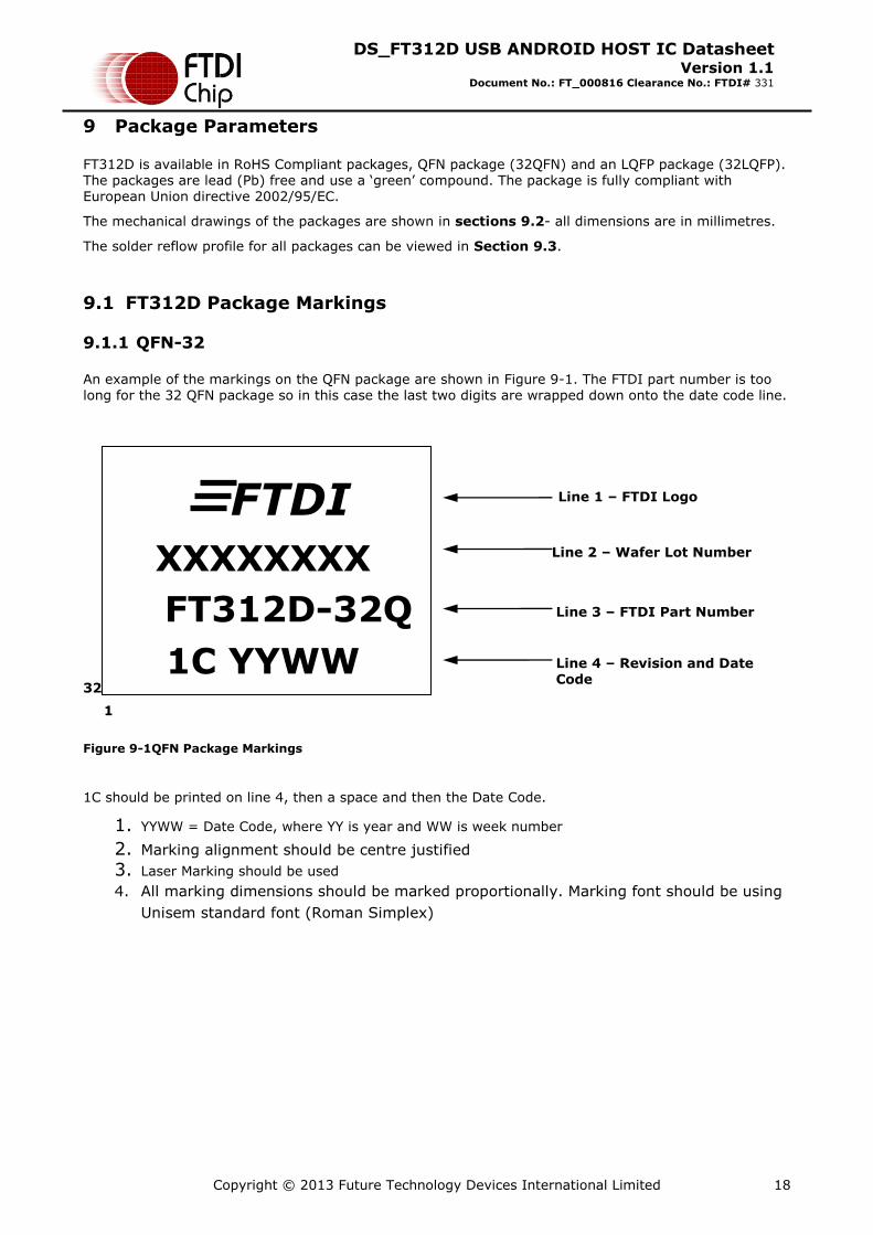
9.1 FT312D Package Markings
9.1.1 QFN-32
An example of the markings on the QFN package are shown in Figure 9-1. The FTDI part number is too long for the 32 QFN package so in this case the last two digits are wrapped down onto the date code line.
Figure 9-1QFN Package Markings
1C should be printed on line 4, then a space and then the Date Code.
1. YYWW = Date Code, where YY is year and WW is week number
2. Marking alignment should be centre justified 3. Laser Marking should be used 4. All marking dimensions should be marked proportionally. Marking font should be using
Unisem standard font (Roman Simplex)
FTDI
I XXXXXXXX
FT312D-32Q
Line 1 – FTDI Logo
Line 4 – Revision and Date Code
Line 2 – Wafer Lot Number
1
32
Line 3 – FTDI Part Number
1C YYWW

Copyright © 2013 Future Technology Devices International Limited 19
DS_FT312D USB ANDROID HOST IC Datasheet
Version 1.1 Document No.: FT_000816 Clearance No.: FTDI# 331
9.1.2 LQFP-32
An example of the markings on the LQFP package are shown in Figure 9-2.
Figure 9-2 LQFP Package Markings
Notes:
1. YYWW = Date Code, where YY is year and WW is week number
2. Marking alignment should be centre justified
3. Laser Marking should be used 4. All marking dimensions should be marked proportionally. Marking font should be using Unisem
standard font (Roman Simplex)
FTD
I XXXXXXXXXX
FT312D-32L
Line 1 – FTDI Logo
Line 4 – Revision, Date Code
Line 2 – Wafer Lot Number
1
32
Line 3 – FTDI Part Number
1C YYWW

Copyright © 2013 Future Technology Devices International Limited 20
DS_FT312D USB ANDROID HOST IC Datasheet
Version 1.1 Document No.: FT_000816 Clearance No.: FTDI# 331
9.2 FT312DPackage Dimensions
9.2.1 QFN-32 Package Dimensions
1
XXXXXXXX
FTDl
1C YYWW
FT312D-32Q
1
Figure 9-3 QFN-32 Package Dimensions
Note: Dimensions are in mm
Note: The centre pad should be connected to the GND plane for improved thermal conduction and noise immunity.

Copyright © 2013 Future Technology Devices International Limited 21
DS_FT312D USB ANDROID HOST IC Datasheet
Version 1.1 Document No.: FT_000816 Clearance No.: FTDI# 331
9.2.2 LQFP-32 Package Dimensions
FTDlXXXXXXXX
1C YYWW
FT312D-32L
PIN #1
PIN #32
Figure 9-4LQFP-32 Package Dimensions
Note: Dimensions are in mm

Copyright © 2013 Future Technology Devices International Limited 22
DS_FT312D USB ANDROID HOST IC Datasheet
Version 1.1 Document No.: FT_000816 Clearance No.: FTDI# 331
9.3 Solder Reflow Profile
Figure 9-5 All packages Reflow Solder Profile

Copyright © 2013 Future Technology Devices International Limited 23
DS_FT312D USB ANDROID HOST IC Datasheet
Version 1.1 Document No.: FT_000816 Clearance No.: FTDI# 331
Profile Feature
Pb Free Solder Process
(green material)
SnPb Eutectic and Pb free (non
green material) Solder Process
Average Ramp Up Rate (Ts to Tp) 3°C / second Max. 3°C / Second Max.
Preheat
- Temperature Min (Ts Min.)
- Temperature Max (Ts Max.)
- Time (ts Min to ts Max)
150°C
200°C
60 to 120 seconds
100°C
150°C
60 to 120 seconds
Time Maintained Above Critical Temperature
TL:
- Temperature (TL)
- Time (tL)
217°C
60 to 150 seconds
183°C
60 to 150 seconds
Peak Temperature (Tp) 260°C see Figure 9-5
Time within 5°C of actual Peak Temperature
(tp) 30 to 40 seconds 20 to 40 seconds
Ramp Down Rate 6°C / second Max. 6°C / second Max.
Time for T= 25°C to Peak Temperature, Tp 8 minutes Max. 6 minutes Max.
Table 9.1Reflow Profile Parameter Values
SnPb Eutectic and Pb free (non green material)
Package Thickness Volume mm3 < 350 Volume mm3 >=350
< 2.5 mm 235 +5/-0 deg C 220 +5/-0 deg C ≥ 2.5 mm 220 +5/-0 deg C 220 +5/-0 deg C
Pb Free (green material) = 260 +5/-0 deg C
Table 9.2 Package Reflow Peak Temperature

Copyright © 2013 Future Technology Devices International Limited 24
DS_FT312D USB ANDROID HOST IC Datasheet
Version 1.1 Document No.: FT_000816 Clearance No.: FTDI# 331
10 Contact Information
Head Office – Glasgow, UK
Future Technology Devices International Limited Unit 1, 2 Seaward Place, Centurion Business Park Glasgow G41 1HH United Kingdom Tel: +44 (0) 141 429 2777 Fax: +44 (0) 141 429 2758
E-mail (Sales) [email protected] E-mail (Support) [email protected] E-mail (General Enquiries) [email protected]
Branch Office – Taipei, Taiwan
Future Technology Devices International Limited (Taiwan) 2F, No. 516, Sec. 1, NeiHu Road Taipei 114 Taiwan, R.O.C. Tel: +886 (0) 2 8791 3570 Fax: +886 (0) 2 8791 3576 E-mail (Sales) [email protected] E-mail (Support) [email protected] E-mail (General Enquiries) [email protected]
Branch Office – Oregon, USA
Future Technology Devices International Limited (USA)
7130 SW Fir Loop Tigard, OR 97223
USA Tel: +1 (503) 547 0988 Fax: +1 (503) 547 0987 E-Mail (Sales) [email protected] E-Mail (Support) [email protected] E-Mail (General Enquiries) [email protected]
Branch Office – Shanghai, China
Room 1103, No. 666 West Huaihai Road, Shanghai, 200052 China Tel: +86 21 62351596 Fax: +86 21 62351595 E-mail (Sales) [email protected]
E-mail (Support) E-mail (General Enquiries)

Copyright © 2013 Future Technology Devices International Limited 25
DS_FT312D USB ANDROID HOST IC Datasheet
Version 1.1 Document No.: FT_000816 Clearance No.: FTDI# 331
Appendix A – References
Useful Links
http://www.ftdichip.com/Support/Documents/White_Papers/WP_001_Connecting_%20Peripherals_to_an
_Android_%20Platform.pdf
http://www.ftdichip.com/Support/Documents/ProgramGuides/FT31XD_Android_programmer_guide(FT_000532).pdf
Useful utilities and examples firmware
http://www.ftdichip.com/Support/Utilities/FT312D_Configuration_V010000.zip
http://www.ftdichip.com/Support/SoftwareExamples/Android_Projects.htm

Copyright © 2013 Future Technology Devices International Limited 26
DS_FT312D USB ANDROID HOST IC Datasheet
Version 1.1 Document No.: FT_000816 Clearance No.: FTDI# 331
Appendix B - List of Figures and Tables
List of Figures
Figure 2.1FT312D Block Diagram .................................................................................................... 3
Figure 3.1QFN Schematic Symbol ................................................................................................... 6
Figure 5-1 UART Receive Waveform .............................................................................................. 10
Figure 5-2 UART Transmit Waveform ............................................................................................ 10
Figure 5-3 UART RXD and TXD connection gated by Enumeration ..................................................... 11
Figure 5-4 Inverting Gate Control signal to enable GPS module(active high enable) ............................ 11
Figure 8.1Application Example showing USB to UART Converter ....................................................... 16
Figure 8.2Application Example showing USB to RS232 Converter ...................................................... 17
Figure 9-1QFN Package Markings .................................................................................................. 18
Figure 9-2 LQFP Package Markings ................................................................................................ 19
Figure 9-3 QFN-32 Package Dimensions ........................................................................................ 20
Figure 9-4LQFP-32 Package Dimensions ........................................................................................ 21
Figure 9-5 All packages Reflow Solder Profile ................................................................................. 22
List of Tables
Table 3.1 Power and Ground .......................................................................................................... 6
Table 3.2 Function pins ................................................................................................................. 7
Table 4.1Default Descriptor Strings ................................................................................................. 9
Table 6.1 Error Detection ............................................................................................................. 12
Table 7.1 Absolute Maximum Ratings ............................................................................................ 13
Table 7.2Operating Voltage and Current ........................................................................................ 14
Table 7.3I/O Pin Characteristics .................................................................................................... 14
Table 7.4USB I/O Pin (USBDP, USBDM) Characteristics ................................................................... 15
Table 7.5Crystal Oscillator 1.8 Volts DC Characteristics ................................................................... 15
Table 7.6 ESD and Latch-up Specifications ..................................................................................... 15
Table 9.1Reflow Profile Parameter Values ...................................................................................... 23
Table 9.2 Package Reflow Peak Temperature .................................................................................. 23
Copyright © 2013 Future Technology Devices International Limited 27
DS_FT312D USB ANDROID HOST IC Datasheet
Version 1.1 Document No.: FT_000816 Clearance No.: FTDI# 331
Appendix C - Revision History
Document Title: USB Android Host ICDS_FT312D
Document Reference No.: FT_000816
Clearance No.: FTDI# 331
Product Page: http://www.ftdichip.com/FTProducts.htm
Document Feedback: Send Feedback
Version 1.0 Initial Release Feb2013
Version 1.1 Note added on USB enumeration to be completed before
Receiving data in RXD Nov 2013