
Performance Analysis of Video Transmission Over IEEE 802.11a/e WLANs

FPGA BASED IMPLEMENTATION OF IEEE 802.11a
PHYSICAL LAYER
a thesis
submitted to the department of electrical and
electronics engineering
and the institute of engineering and sciences
of bilkent university
in partial fulfillment of the requirements
for the degree of
master of science
By
MUSTAFA INCE
December 2010

I certify that I have read this thesis and that in my opinion it is fully adequate,
in scope and in quality, as a thesis for the degree of Master of Science.
Prof. Dr. Abdullah ATALAR(Supervisor)
I certify that I have read this thesis and that in my opinion it is fully adequate,
in scope and in quality, as a thesis for the degree of Master of Science.
Prof. Dr. Yalcın TANIK
I certify that I have read this thesis and that in my opinion it is fully adequate,
in scope and in quality, as a thesis for the degree of Master of Science.
Assist. Prof. Dr. Defne AKTAS
Approved for the Institute of Engineering and Sciences:
Prof. Dr. Levent OnuralDirector of Institute of Engineering and Sciences
ii

ABSTRACT
FPGA BASED IMPLEMENTATION OF IEEE 802.11a
PHYSICAL LAYER
MUSTAFA INCE
M.S. in Electrical and Electronics Engineering
Supervisor: Prof. Dr. Abdullah ATALAR
December 2010
Orthogonal Frequency Division Multiplexing (OFDM) is a multicarrier transmis-
sion technique, in which a single bitstream is transmitted over a large number of
closely-spaced orthogonal subcarriers. It has been adopted for several technolo-
gies, such as Wireless Local Area Networks (WLAN), Digital Audio and Ter-
restrial Television Broadcasting and Worldwide Interoperability for Microwave
Access (WiMAX) systems.
In this work, IEEE802.11a WLAN standard was implemented on Field Pro-
grammable Gate Array (FPGA) for being familiar with the implementation prob-
lems of OFDM systems. The algorithms that are used in the implementation
were firstly built up in MATLAB environment and the performance of system
was observed with a simulator developed for this purpose. The transmitter and
receiver FPGA implementations, which support the transmission rates from 6
to 54 Mbps, were designed in Xilinx System Generator Toolbox for MATLAB
Simulink environment. The modulation technique and the Forward Error Cod-
ing (FEC) rate used at the transmitter are automatically adjusted by the desired
bitrate as BPSK, QPSK, 16QAM or 64QAM and 1/2, 2/3 or 3/4, respectively.
iii

The transceiver utilizes 5986 slices, 45 block RAMs and 73 multipliers of a Xil-
inx Virtex-4 sx35 chip corresponding to % 39 of the resources. In addition, the
FPGA implementation of the transceiver was also tested by constructing a wire-
less link between two Lyrtech Software Defined Radio Development Kits and
the bit error rate of the designed system was measured by performing a digital
loop-back test under an Additive White Gaussian Noise (AWGN) channel.
Keywords: OFDM, IEEE802.11a, FPGA, FFT, Viterbi Decoder
iv

OZET
IEEE 802.11A FIZIKSEL KATMANININ FPGA TABANLI
GERCEKLENMESI
MUSTAFA INCE
Elektrik ve Elektronik Muhendisligi Bolumu Yuksek Lisans
Tez Yoneticisi: Prof. Dr. Abdullah ATALAR
Aralık 2010
Dikgen Frekans Bolmeli Cogullama, yuksek hızlı bir veriyi birbirine yakın
aralıktaki cok sayıda dikgen alt tasıyıcılar uzerinden ileten cok tasıyıcılı bir
modulasyon teknigidir. Bu teknik basta Kablosuz Yerel Alan Agları (WLAN)
olmak uzere Sayısal Ses ve Televizyon Yayıncılıgı ve Dunya Capında Mikrodalga
Erisimi icin Birarada Calısabilirlik (WiMAX) gibi bircok standart tarafından
benimsenmistir.
Bu calısmada, IEEE802.11a WLAN standardı, OFDM sistemlerinin uygu-
lama sorunlarını kavramak amacıyla Alanda Programlanabilir Kapı Dizileri
(FPGA) uzerinde gerceklenmistir. Gerceklemede kullanılan algoritmalar ilk
olarak MATLAB ortamında gelistirilmis ve sistemin performansı yine bu ortamda
tasarlanan bir simulator aracılıgıyla gozlemlenmistir. Saniyede 6 Mb’den 54 Mb’e
kadar veri iletisim hızlarını destekleyen alıcı ve vericinin FPGA gerceklemeleri
MATLAB Simulink ortamında Xilinx firmasının “System Generator” arayuzu
ile tasarlanmıstır. Verici unitesinde kullanılan modulasyon teknigi ve Ileri Hata
Duzeltme (FEC) oranı, istenen bit hızına gore sırasıyla BPSK, QPSK, 16QAM
v
veya 64QAM ve 1/2, 2/3 veya 3/4 olacak sekilde otomatik olarak ayarlanmak-
tadır. Tasarlanan alıcı-verici donanımının kaynak kullanımı ise 5986 slice, 45 blok
RAM ve 73 carpıcıdan ibaret olup, Xilinx Virtex-4 sx35 yongasının % 39’unu
kaplamaktadır. Ayrıca, alıcı-verici birimlerinin FPGA gerceklemesi, iki adet
Lyrtech Yazılım Tanımlı Radyo (SDR) Gelistirme Donanımı arasında kablosuz
baglantı kurularak test edilmis ve tasarlanan sistemin bit hata oranı, Toplan-
abilir Beyaz Gaussian Gurultulu (AWGN) kanal uzerinden sayısal dongu testi
yapılarak olculmustur.
Anahtar Kelimeler: Dikgen Frekans Bolmeli Cogullama (OFDM), IEEE802.11a,
FPGA, Hızlı Fourier Donusumu (FFT), Viterbi Kodcozucu
vi

ACKNOWLEDGMENTS
I would like to thank my advisor Prof. Dr. Abdullah ATALAR for his
guidance and suggestions throughout my graduate education and my research.
I would also like to thank the members of the thesis committee for reviewing
the thesis.
I would like to express my appreciation to my beloved wife, Ferda, for her
support and patience during my study.
Finally, I would also like to thank The Scientific and Technological Research
Council of Turkey (TUBITAK) for the financial support during my study.
vii

Contents
1 INTRODUCTION 1
1.1 Background on OFDM . . . . . . . . . . . . . . . . . . . . . . . . 1
1.2 Thesis Objective and Outline . . . . . . . . . . . . . . . . . . . . 5
2 THE IEEE 802.11a STANDARD 6
2.1 General Structure . . . . . . . . . . . . . . . . . . . . . . . . . . . 6
2.2 The Frame Format of IEEE 802.11a . . . . . . . . . . . . . . . . . 7
2.3 IEEE802.11a Transmitter Blocks . . . . . . . . . . . . . . . . . . 9
2.3.1 Data Scrambler . . . . . . . . . . . . . . . . . . . . . . . . 10
2.3.2 Convolutional Encoder . . . . . . . . . . . . . . . . . . . . 10
2.3.3 Data Interleaving . . . . . . . . . . . . . . . . . . . . . . . 10
2.3.4 Sub-carrier Modulation . . . . . . . . . . . . . . . . . . . . 11
3 IEEE 802.11a RECEIVER DESIGN 12
3.1 Receiver Architecture . . . . . . . . . . . . . . . . . . . . . . . . . 12
viii

3.1.1 Frame Detection . . . . . . . . . . . . . . . . . . . . . . . 14
3.1.2 Coarse Frequency Synchronization . . . . . . . . . . . . . . 15
3.1.3 Timing Synchronization . . . . . . . . . . . . . . . . . . . 17
3.1.4 Fine Frequency Synchronization . . . . . . . . . . . . . . . 19
3.1.5 Channel Estimation . . . . . . . . . . . . . . . . . . . . . . 19
3.1.6 Channel Equalization . . . . . . . . . . . . . . . . . . . . . 21
3.2 IEEE 802.11a MATLAB Simulator . . . . . . . . . . . . . . . . . 22
4 FPGA IMPLEMENTATION 25
4.1 Transmitter Implementation . . . . . . . . . . . . . . . . . . . . . 26
4.1.1 Subsystem 1: ProcessControl . . . . . . . . . . . . . . . . 27
4.1.2 Subsystem 2: FecAndInterleaver . . . . . . . . . . . . . . . 28
4.1.3 Subsystem 3: CarrierModulation . . . . . . . . . . . . . . 28
4.1.4 Subsystem 4: CyclicIFFT . . . . . . . . . . . . . . . . . . 30
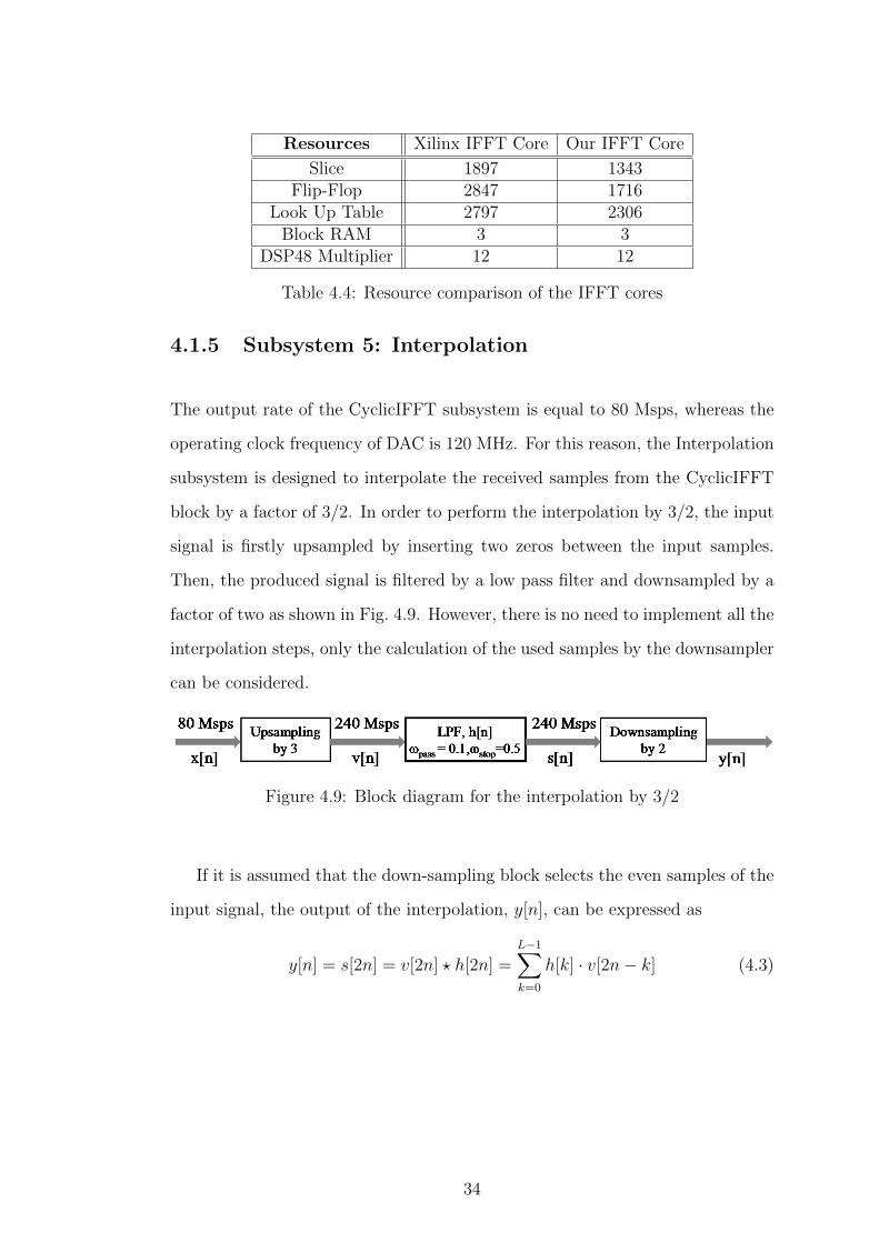
4.1.5 Subsystem 5: Interpolation . . . . . . . . . . . . . . . . . . 34
4.2 Receiver Implementation . . . . . . . . . . . . . . . . . . . . . . . 35
4.2.1 Down Conversion to Baseband . . . . . . . . . . . . . . . . 37
4.2.2 Preamble Decoding . . . . . . . . . . . . . . . . . . . . . . 38
4.2.3 Channel Estimation . . . . . . . . . . . . . . . . . . . . . . 41
4.2.4 Channel Equalizer . . . . . . . . . . . . . . . . . . . . . . 42
ix

4.2.5 Subcarrier Demodulation . . . . . . . . . . . . . . . . . . . 44
4.2.6 Viterbi Decoder . . . . . . . . . . . . . . . . . . . . . . . . 45
4.3 Performance Measurements . . . . . . . . . . . . . . . . . . . . . 48
5 CONCLUSION AND FUTURE WORK 52
APPENDIX 54
A Lyrtech SFF SDR Development Platform 54
x
List of Figures
1.1 Block diagram of multi-carrier transmitter . . . . . . . . . . . . . 2
1.2 Spectrum of (a) a single sub-carrier and (b) OFDM signal . . . . 3
1.3 Cyclic extension of the OFDM symbol . . . . . . . . . . . . . . . 4
2.1 Frame format of the IEEE 802.11a Standard . . . . . . . . . . . . 8
2.2 Block diagram of the IEEE 802.11a transmitter . . . . . . . . . . 10
2.3 The frequency allocation of IEEE 802.11a sub-carriers . . . . . . . 11
3.1 Block diagram of IEEE 802.11a receiver architecture . . . . . . . 13
3.2 Decision variables, (a) Power method, (b) Schmidl and Cox method 14
3.3 Schmidl and Cox delay and correlate algorithm . . . . . . . . . . 15
3.4 (a) Autocorrelation metric, (b) Cross correlation metric . . . . . . 17
3.5 Performance of the timing synchronization algorithm . . . . . . . 18
3.6 Runtime snapshot of the IEEE802.11a Matlab Simulator . . . . . 23
4.1 System Generator model of the transmitter . . . . . . . . . . . . . 26
xi

4.2 Timing diagram of the transmitter pipeline structure . . . . . . . 27
4.3 Implementation of the FecAndInterleaver subsystem . . . . . . . . 28
4.4 Carrier Modulation subsystem . . . . . . . . . . . . . . . . . . . . 30
4.5 Radix-22 SDF butterfly structure for 16 point IFFT . . . . . . . . 31
4.6 Fpga implementation of the Butterfly 1 in Stage 1 . . . . . . . . . 32
4.7 Complex multiplier implementation with cascaded DSP48 slices . 33
4.8 Illustration of the OFDM symbol windowing . . . . . . . . . . . . 33
4.9 Block diagram for the interpolation by 3/2 . . . . . . . . . . . . . 34
4.10 Interpolation filter implementation . . . . . . . . . . . . . . . . . 35
4.11 System Generator model of the receiver . . . . . . . . . . . . . . . 36
4.12 Down conversion schema of the received signal . . . . . . . . . . . 38
4.13 Implementation of the delay and correlation algorithm . . . . . . 39
4.14 Implementation of the correlation filter, h1[n] . . . . . . . . . . . 40
4.15 Block schema of the chanEstimation subsystem . . . . . . . . . . 41
4.16 Channel Equalization subsystem . . . . . . . . . . . . . . . . . . . 42
4.17 (a)Trellis diagram of the Viterbi decoder, (b) butterfly structure . 46
4.18 System Generator block diagram of the Viterbi decoder . . . . . . 46
4.19 Block diagram of butterfly Add-Compare-Select unit . . . . . . . 47
4.20 Timing diagram of the trace back memory access . . . . . . . . . 48
4.21 Snapshot of the User Interface Program . . . . . . . . . . . . . . . 48
xii

4.22 Runtime snapshot of (a)BPSK and (b)QPSK constellations . . . . 49
4.23 Runtime snapshot of (a)16-QAM and (b)64-QAM constellations . 49
4.24 Runtime snapshot of bit error rate measurement . . . . . . . . . . 50
4.25 BER performance of QPSK modulation . . . . . . . . . . . . . . . 50
4.26 BER performance of 16-QAM modulation . . . . . . . . . . . . . 51
4.27 BER performance of 64-QAM modulation . . . . . . . . . . . . . 51
A.1 Lyrtech SFF SDR Development Platform . . . . . . . . . . . . . . 54
A.2 Block diagram of the Data Conversion module . . . . . . . . . . . 55
A.3 Direct Quadrature RF Transmitter . . . . . . . . . . . . . . . . . 56
A.4 Super Heterodyne RF Receiver . . . . . . . . . . . . . . . . . . . 56
xiii

List of Tables
2.1 Rate dependent parameters in IEEE 802.11a standard . . . . . . . 9
4.1 BPSK and QPSK modulation IQ mapping . . . . . . . . . . . . . 29
4.2 16 QAM modulation IQ mapping . . . . . . . . . . . . . . . . . . 29
4.3 64 QAM modulation IQ mapping . . . . . . . . . . . . . . . . . . 29
4.4 Resource comparison of the IFFT cores . . . . . . . . . . . . . . . 34
4.5 One period of the short preamble sequence . . . . . . . . . . . . . 39
xiv

Dedicated to Ferda INCE

LIST OF ABBREVIATIONS
ADC Analog to Digital Converter
ADSL Asymmetric Digital Subscriber Line
AWGN Additive White Gaussian Noise
BER Bit Error Rate
BPSK Binary Phase Shift Keying
CP Cyclic Prefix
DAC Digital to Analog Converter
FEC Forward Error Correction
FFT Fast Fourier Transformation
FPGA Field Programmable Gate Array
GUI Graphical User Interface
ICI Inter-carrier Interference
IFFT Inverse Fast Fourier Transformation
ISI Inter-symbol Interference
LFSR Linear Feedback Shift Register
LSB Least Significant Bit
MAC Medium Access Control
PLCP Physical Layer Convergence Procedure
PSDU Physical Layer Service Data Unit
OFDM Orthogonal Frequency Division Multiplexing
RF Radio Frequency
SDR Software Defined Radio
SNR Signal to Noise Ratio
SFF Small Form Factor
QAM Quadrature Amplitude Modulation
QPSK Quadrature Phase Shift Keying
WiMAX Worldwide Interoperability for Microwave Access
WLAN Wireless Local Area Network
xvi

Chapter 1
INTRODUCTION
1.1 Background on OFDM
The Orthogonal Frequency Division Multiplexing (OFDM), which is a multi-
carrier modulation technique, has gained a great deal of interest during the last
few decades. It has been adopted for several broadband communication systems;
such as digital video broadcasting, Asymmetric Digital Subscriber Line (ADSL)
services, Wireless Local Area Networks (IEEE 802.11a/g/n), and Worldwide
Interoperability for Microwave Access (WiMAX) systems (IEEE 802.16e) and
third generation cellular systems [1]. In this modulation technique, a high bit-
rate data stream with a bandwidth of B is split into N parallel lower bit-rate
sub-streams and each of these sub-streams which have a bandwidth of B/N is
transmitted over an orthogonal sub-carrier, as shown in Fig. 1.1.
One of the main reasons of using the OFDM scheme is its ability to adapt
to severe channel conditions without using a complex equalizer. If the number
of sub-carriers, N, is selected large enough, the bandwidth of each sub-carrier
becomes smaller than the coherence bandwidth of the channel. In this case,
the channel characteristic of each sub-carrier exhibits approximately flat fading
1

Figure 1.1: Block diagram of multi-carrier transmitter
and therefore the distortions on the channel can be compensated by a one-tap
equalizer. Besides, the OFDM scheme is also robust against fading caused by
the multi-path propagation. Whereas a deep fade may cause a failure in a single
carrier system, only a small part of the sub-carriers in an OFDM system is
destroyed by the fading and lost information on the destroyed sub-carriers can
be recovered by using forward error correction (FEC) codes [2].
In a conventional multi-carrier system, the frequency band is divided into
non-overlapping adjacent sub-bands where adjacent sub-carriers are separated
by more than the two sided bandwidth of each. This technique eliminates the
inter-carrier interference (ICI) by avoiding the spectral overlaps, but it causes
inefficiency in the use of available frequency band. The OFDM scheme over-
comes this inefficiency by selecting the sub-carrier frequencies as mathematically
orthogonal to each other. The word “orthogonal” means that the frequency of
each sub-carrier is an integer multiple of 1/T, where T is the symbol duration [3].
By this way, as shown in Fig. 1.2b, the frequency band is used 50% more effi-
ciently than a conventional system without causing an ICI.
After selecting the frequencies, fk, in Fig. 1.1 as k/T , the equation of the
transmitted signal in multi-carrier systems can be written as in Eq. (1.1). This
equation can be transformed into discrete time by replacing the continuous time
variable, t, by nT/N , where T/N is equal to sampling period. It can be shown
2

(a) (b)
Figure 1.2: Spectrum of (a) a single sub-carrier and (b) OFDM signal
that the transmitted signal in Eq. (1.2) is the Inverse Discrete Fourier Transfor-
mation (IDFT) of N sequential serial symbols. If the number of the sub-carriers,
N , is selected as the power of 2, the OFDM transmitter and receiver can be eas-
ily implemented by using IFFT (Inverse Fast Fourier Transformation) and FFT,
respectively.
x (t) =1√T
N−1∑k=0
XkΠ
(t
T− 1
2
)exp
(j2π
k
Tt
)(1.1)
x [n] =1√N
N−1∑k=0
Xk · exp
(j2π
kn
N
)(1.2)
The OFDM scheme also eliminates the inter-symbol interference by inserting
a cyclic prefix (CP), as illustrated in Fig. 1.3, between the adjacent symbols
in the transmitter, and removing it at the receiver. Despite the fact that the
cyclic prefix introduces a power loss at the transmitter, it is a simple technique
to preserve the orthogonality of the sub-carriers through a multi-path channel.
Unless the maximum delay spread of the channel exceeds the length of the cyclic
prefix, an FFT based OFDM receiver can gather the delayed echoes of each
transmitted sub-carrier in the corresponding frequency bin. Furthermore, the
cyclic prefix can suppress the timing offsets smaller than itself by decreasing the
maximum allowable multi-path delay, and so the OFDM systems become less
3

sensitive to symbol timing offsets than a single carrier system through the use of
cyclic prefix.
Figure 1.3: Cyclic extension of the OFDM symbol
Despite these advantages, the OFDM technique has also some disadvantages
compared with a single carrier modulation. The most important problem of
the OFDM systems is that the transmitted signal has a relatively large peak-to-
average-power ratio (PAPR) due to the summation of many narrowband signals
which have independent phases. To cope with this problem, the OFDM systems
require a linear transmitter circuitry, which suffers from poor power efficiency,
and high resolution digital-to-analog (DAC) and analog-to-digital (ADC) con-
verters.
In addition to PAPR problem, the OFDM systems are also more sensitive to
carrier frequency offset between the transmitter and receiver. As the frequency
spacing between the adjacent sub-carriers is very small, accurate frequency syn-
chronization is needed for OFDM systems. If there exists a residual frequency
offset, ∆f , that has not been corrected by the receiver, it introduces ICI on the
system and creates a time-variant phase rotation on the symbol constellation. As
illustrated in Fig. 1.2b, a small ∆f causes ICI by corrupting the orthogonality
of the sub-carriers.
4
1.2 Thesis Objective and Outline
The IEEE802.11a standard for the Wireless Local Area Networks (WLAN) is
the first IEEE standard which utilizes the OFDM modulation technology. In
this thesis, the aim is to implement the physical layer of IEEE802.11a standard
on Field Programmable Gate Array (FPGA) for being familiar with the imple-
mentation problems of the OFDM systems. The advantages and disadvantages
of the OFDM technology over the conventional multicarrier and single carrier
systems are discussed in this chapter. The rest of the thesis is organized in
four chapters as follows. Chapter 2 briefly summarizes the specifications of the
IEEE802.11a standard. Chapter 3 describes the receiver model designed in MAT-
LAB environment by focusing on the synchronization algorithms and presents
the MATLAB simulator developed for observing the performance of the overall
system. Chapter 4 explains the implementation of the transmitter and receiver
FPGA cores in detail and gives the measured bit error rate (BER) performance
of the designed system. Finally, Chapter 5 contains a brief conclusion about the
thesis and presents the possible future work.
5

Chapter 2
THE IEEE 802.11a STANDARD
The IEEE 802.11a, which is published by the IEEE LAN/MAN Standards Com-
mittee (IEEE 802.11) in 1999, is a wireless local area network computer commu-
nication standard in the 5 GHz frequency band [4]. It defines the requirements
for the physical layer (PHY) and the medium access control (MAC) layer. The
physical layer defines how the raw bits in a packet are transmitted over a commu-
nication link and specifies the encoding and signaling functions that transform
the raw bits into the radio waves. The MAC layer defines the interface between
the physical layer and the interface bus of the machine. In this chapter, the
physical layer of IEEE 802.11a standard will be explained briefly.
2.1 General Structure
The IEEE802.11a is the first standard of IEEE 802.11 committee which uses
the Orthogonal Frequency Division Multiplexing (OFDM) as the modulation
technique. It transmits an analog waveform, converted from a digital signal,
over the Unlicensed-National Information Infrastructure (U-NII) bands, 5.15-
5.25 GHz, 5.25-5.35 GHz and 5.725-5.825 GHz. Each band contains 4 channels
6
with a bandwidth of 20 MHz and the output power limits of these bands are
40 mW, 200 mW and 800 mW, respectively [4].
The IEEE802.11a standard divides the 20 MHz channel into 64 sub-carriers
with a frequency spacing of 312.5 KHz and uses 48 of them as data sub-carriers,
4 of them as pilot sub-carriers and the others as guard sub-carriers to avoid the
adjacent channel interference. Whereas the pilot sub-carriers transmit a prede-
termined symbol sequence for channel tracking, the data sub-carriers convey the
information stream modulated by using Phase Shift Keying (PSK) or Quadrature
Amplitude Modulation (QAM) techniques.
The OFDM scheme enables the IEEE802.11a to transfer the raw data at a
maximum rate of 54 Mbps. The standard also supports the data rates 6, 9, 12,
18, 24, 36 and 48 Mbps by changing the modulation type and the Forward Error
Correction (FEC) coding rate of the data sub-carriers. The symbol duration is
specified as 4 microseconds in the standard and 800 ns of it is used for cyclic
prefix to ensure an ISI-free reception of the transmitted symbols over a channel
with a delay spread up to 250 ns [5].
2.2 The Frame Format of IEEE 802.11a
Each frame in the physical layer of IEEE 802.11a includes Physical Layer Conver-
gence Procedure (PLCP) Preambles, PLCP header, and Physical Layer Service
Data Unit (PSDU), tail and pad bits, as shown in Fig. 2.1. The PLCP Pream-
ble consists of 10 short preambles and two long preambles. The short preambles
are used for frame detection, automatic gain control and timing synchronization.
The frequency offset and channel response is also estimated through the long
preambles that are sent immediately after the short preamble.
7

Figure 2.1: Frame format of the IEEE 802.11a Standard
The length of the short preambles is 0.8 µsec which equals to one fifth of a
regular symbol period. They are generated by taking the IFFT of the following
sequence, S−26:26, which produces a periodic signal with a period of 16 samples.
By repeating the produced signal two times after adding the cyclic prefix, ten
identical short preamble symbols are generated.
S−26:26 =√
13/6(0, 0, 1 + j, 0, 0, 0,−1− j, 0, 0, 0, 1 + j, 0, 0, 0,−1− j, 0, 0, 0,
−1− j, 0, 0, 0, 1 + j, 0, 0, 0, 0, 0, 0, 0,−1− j, 0, 0, 0,−1− j, 0, 0, 0, 1 + j,
0, 0, 0, 1 + j, 0, 0, 0, 1 + j, 0, 0, 0, 1 + j, 0, 0) (2.1)
The long preamble sequence is composed of a cyclic prefix and two identical
long preamble symbols. Unlike the other OFDM symbols, the length of the cyclic
prefix for this sequence is equal to 32 samples. The reason of this is the use of the
long preambles for fine frequency offset estimation by avoiding the discontinuity
between the consecutive symbols. All the 52 sub-carriers are used during the
generation of the long preambles and they are modulated by the elements of the
following sequence.
L−26:26 = (1, 1,−1,−1, 1, 1,−1, 1,−1, 1, 1, 1, 1, 1, 1,−1,−1, 1, 1,−1, 1,−1, 1,
1, 1, 1, 0, 1,−1,−1, 1, 1,−1, 1,−1, 1,−1,−1,−1,−1,−1, 1, 1,−1,−1, 1,
−1, 1,−1, 1, 1, 1, 1) (2.2)
The first symbol after the long training symbols is named as Signal Field,
which is transmitted by using BPSK and coding rate at 1/2, and it contains
8

the Rate and Length parameters. The information about the modulation type
and FEC rate that is used in the rest of the frame is conveyed through 4 bits
Rate parameter, Table 2.1, and the Length parameter indicates the number of
information bytes in the PSDU [4].
Rate Data rate Modulation CodingRate(R)
Coded bitsper symbol
Data bitsper symbol
1101 6 Mbps BPSK 1/2 48 241111 9 Mbps BPSK 3/4 48 360101 12 Mbps QPSK 1/2 96 480111 18 Mbps QPSK 3/4 96 721001 24 Mbps 16QAM 1/2 192 961011 36 Mbps 16QAM 3/4 192 1440001 48 Mbps 64QAM 2/3 288 1920011 54 Mbps 64QAM 3/4 288 216
Table 2.1: Rate dependent parameters in IEEE 802.11a standard
The service field, transmitted after the signal field, contains of 16 bits and is
used for synchronizing the data descrambler in the receiver. Then, the OFDM
frame conveys the PSDU payload which is sent by the MAC layer. The six zero
tail bits follow the PSDU to force the Viterbi decoder in the receiver to zero
state. Finally, the end of the frame is filled with the pad bits so that the number
of bits in the data symbols becomes a multiple of the coded bits in an OFDM
symbol.
2.3 IEEE802.11a Transmitter Blocks
The IEEE802.11a standard specifies only the transmission part of the physical
layer and gives the performance requirements for the receiver. This allows dif-
ferent manufacturers to develop their own receiver solutions that are compatible
with each other. The specified transmission chain by the standard is illustrated
in Fig. 2.2. The transmitter blocks in this chain are briefly explained in the
following subsections.
9

Figure 2.2: Block diagram of the IEEE 802.11a transmitter
2.3.1 Data Scrambler
The IEEE 802.11a transmitter uses a data scrambler using a pseudo random
binary sequence (PRBS) to randomize the all information bits, except the signal
field, in order not to transmit a long streams of ones or zeros. The scrambler
uses the polynomial S(x) = x7 + x4 + 1 which generates a cyclic sequence of
length 127 and the initial state of the scrambler is set randomly at the beginning
of the transmission. The receiver estimates the initial state of the scrambler by
observing the first seven bits of the Service field.
2.3.2 Convolutional Encoder
In order to achieve a reliable data transfer, all the information bits in the frame,
including the Signal field, are coded with a convolutional encoder. The IEEE
802.11a standard uses the industry standard generator polynomials, g0 = 1338
and g1 = 1718 to produce two bits of output for each input bit, and supports the
1/2, 2/3 and 3/4 coding rates by puncturing the data prior to transmission [4].
2.3.3 Data Interleaving
Block interleaving technique is used in the IEEE 802.11a standard for improving
the performance of forward error correcting codes. All the bits at the output of
the convolutional encoder are interleaved by a block interleaver and the size of
the interleaver block is determined by the number of the coded bits per OFDM
symbol, NCBPS. The interleaver consist of two permutation steps and at the
10

first permutation step, the adjacent coded bits are assigned to non-adjacent sub-
carriers. By the second permutation step, the bit index of the consecutive coded
bits onto the constellation is changed continuously in order to avoid the long
runs of LSB bits [4].
2.3.4 Sub-carrier Modulation
In the IEEE 802.11a transmitter, a 64 point IFFT multiplexes the orthogonal
sub-carriers and the sub-carriers are renumbered as in Fig. 2.3 before performing
the Fourier transformation. Only 48 of them are used for data transmission
and they are modulated by using BPSK, QPSK, 16-QAM or 64-QAM according
to the Rate parameter. The sub-carriers P−21, P−7, P7 and P21 are dedicated
to comb-type pilot signals which are used to track the phase variations due to
the time varying channel or a frequency offset error. The pilot sub-carriers are
modulated by using BPSK and to prevent the generation of spectral lines, they
transmit a pseudo random binary sequence generated by the same polynomial
used in the scrambler.
Figure 2.3: The frequency allocation of IEEE 802.11a sub-carriers
11
Chapter 3
IEEE 802.11a RECEIVER
DESIGN
As mentioned in Chapter 2, the IEEE 802.11a standard does not specify the
structure of the receiver. For this reason, before implementing the IEEE 802.11a
transceiver onto the FPGA, we firstly designed the receiver in MATLAB envi-
ronment. In addition, we also developed a simulator to observe the performance
of the receiver and to ensure that our receiver solution is compatible with the
transmitter specified in the standard. In this chapter, the algorithms that are
used in the receiver and the MATLAB simulator will be explained in detail.
3.1 Receiver Architecture
The Fig. 3.1 shows the base-band receiver architecture for the IEEE 802.11a
standard. The receiver obtains the base-band incoming signal from an analog-
to-digital converter (ADC) with a sampling rate of 20 MHz. Then, it basically
performs the operations of the transmitter, shown in Fig. 2.2, in a reverse order
to reconstruct the transmitted sequence. Unlike the transmitter, the receiver
12
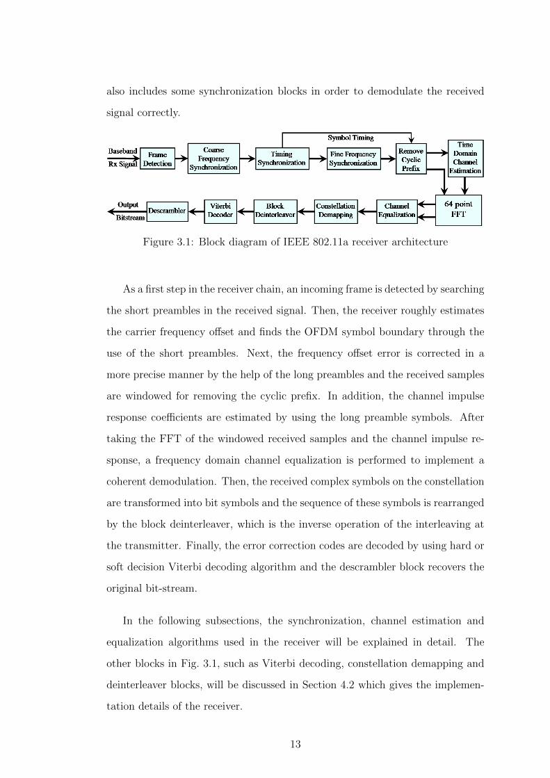
also includes some synchronization blocks in order to demodulate the received
signal correctly.
Figure 3.1: Block diagram of IEEE 802.11a receiver architecture
As a first step in the receiver chain, an incoming frame is detected by searching
the short preambles in the received signal. Then, the receiver roughly estimates
the carrier frequency offset and finds the OFDM symbol boundary through the
use of the short preambles. Next, the frequency offset error is corrected in a
more precise manner by the help of the long preambles and the received samples
are windowed for removing the cyclic prefix. In addition, the channel impulse
response coefficients are estimated by using the long preamble symbols. After
taking the FFT of the windowed received samples and the channel impulse re-
sponse, a frequency domain channel equalization is performed to implement a
coherent demodulation. Then, the received complex symbols on the constellation
are transformed into bit symbols and the sequence of these symbols is rearranged
by the block deinterleaver, which is the inverse operation of the interleaving at
the transmitter. Finally, the error correction codes are decoded by using hard or
soft decision Viterbi decoding algorithm and the descrambler block recovers the
original bit-stream.
In the following subsections, the synchronization, channel estimation and
equalization algorithms used in the receiver will be explained in detail. The
other blocks in Fig. 3.1, such as Viterbi decoding, constellation demapping and
deinterleaver blocks, will be discussed in Section 4.2 which gives the implemen-
tation details of the receiver.
13

3.1.1 Frame Detection
The frame detection is the task of deciding whether or not there is an incoming
frame and giving an approximate estimate for the start time of the frame. This
task can be described as a hypothesis testing problem by comparing a decision
variable µ with a predefined threshold, Thr. If the decision variable exceeds the
threshold, it indicates the presence of the frame.
The most well-known algorithm for finding the start boundary of the incoming
frame is to measure the power of the received signal. This algorithm forms a
decision variable µ by taking the ratio of the received signal power inside the
two consecutive windows, as expressed in Eq. (3.1). When a transmitted frame
is not present, the received signal samples, r[n], consists of only noise and the
received power is equal to the noise power. However, during the transmission
of a frame, the input power at the receiver is equal to the sum of the noise and
signal power. So, as shown in Fig. 3.2a, the decision variable µ creates a peak at
the start boundary of the frame.
µ(n) =
∑D−1i=0 |r[n− i]|
2∑D−1i=0 |r[n− i−D]|2
(3.1)
where D is equal to the length of a short preamble symbol.
(a) (b)
Figure 3.2: Decision variables, (a) Power method, (b) Schmidl and Cox method
The power method is an efficient algorithm if the receiver does not have
a priori knowledge of the preambles in the received frame. However, the IEEE
802.11a standard uses a predetermined sequence as a short preamble and repeats
14
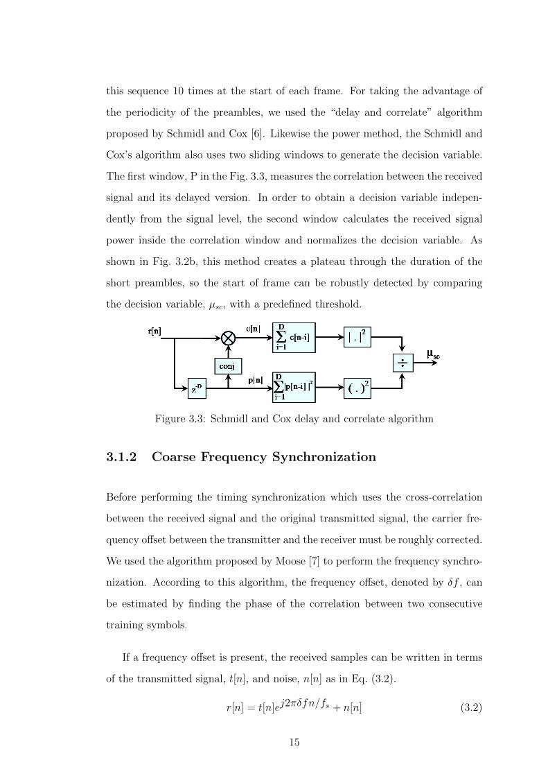
this sequence 10 times at the start of each frame. For taking the advantage of
the periodicity of the preambles, we used the “delay and correlate” algorithm
proposed by Schmidl and Cox [6]. Likewise the power method, the Schmidl and
Cox’s algorithm also uses two sliding windows to generate the decision variable.
The first window, P in the Fig. 3.3, measures the correlation between the received
signal and its delayed version. In order to obtain a decision variable indepen-
dently from the signal level, the second window calculates the received signal
power inside the correlation window and normalizes the decision variable. As
shown in Fig. 3.2b, this method creates a plateau through the duration of the
short preambles, so the start of frame can be robustly detected by comparing
the decision variable, µsc, with a predefined threshold.
Figure 3.3: Schmidl and Cox delay and correlate algorithm
3.1.2 Coarse Frequency Synchronization
Before performing the timing synchronization which uses the cross-correlation
between the received signal and the original transmitted signal, the carrier fre-
quency offset between the transmitter and the receiver must be roughly corrected.
We used the algorithm proposed by Moose [7] to perform the frequency synchro-
nization. According to this algorithm, the frequency offset, denoted by δf , can
be estimated by finding the phase of the correlation between two consecutive
training symbols.
If a frequency offset is present, the received samples can be written in terms
of the transmitted signal, t[n], and noise, n[n] as in Eq. (3.2).
r[n] = t[n]ej2πδfn/fs + n[n] (3.2)
15

Then, the complex correlation, CS[n], between two consecutive short pream-
bles is written as in Eq. (3.3), where NS is equal to 16 which is the length of the
short preamble.
CS[n] =
NS−1∑k=0
r[n− k]× r∗[n− k −NS]
=
NS−1∑k=0
t[n− k]ej2πδf(n−k)/fs × t∗[n− k −NS]ej2πδf(k+NS−n)/fs + noise
= ej2πδfNS/fsNS−1∑k=0
t[n− k]× t∗[n− k −NS] + noise term (3.3)
Due to the periodicity in the short preambles, the transmitted signal, t[n− k], is
equal to the t[n−k−NS] through the correlation window. And so, the Eq. (3.3)
can be simplified as
CS[n] = ej2πδfNS/fsNS−1∑k=0
|t[n− k]|2 + noise term (3.4)
then, the carrier frequency offset can be easily estimated from the phase of CS[n].
δfc =fs∠CS[n]
2πNS
(3.5)
A coarse estimate of the frequency offset is sufficient for the timing syn-
chronization process. So we performed the quantization operation, defined in
Eq. (3.6), on the δfc. This quantization also provides simplicity in the imple-
mentation by considering only a few frequencies instead of the whole frequency
range. ⌊δfc
⌋= sign
(δfS
)·
128 ·∣∣∣δfS∣∣∣fs
+ 0.5
· fs128
(3.6)
where bxc operator denotes the largest integer not greater than x.
After estimating the δfS coarsely, the estimated frequency offset is easily
eliminated from the received signal by multiplying it with a complex exponential
signal whose frequency is equal to the negative of the estimated frequency.
16

3.1.3 Timing Synchronization
After performing the coarse frequency synchronization process, the next task of
the receiver is the timing synchronization which finds the start point of OFDM
symbols. This task is one of the most critical issues in the receiver design be-
cause a timing synchronization error may cause significant ISI which degrades
the receiver performance directly.
In order to find the symbol start point accurately, we made the timing syn-
chronization in two steps. In the first step, the autocorrelation metric, M [n] in
Eq. (3.7), is calculated by using the delay and correlate algorithm. The length
of the correlation and delay block is selected as half of the total duration of the
short preambles so that the M [n] metric creates a peak at the end of the last
short preamble, Fig. 3.4a. Hence, a coarse estimation of the time offset can be
easily obtained by using the Eq. (3.8).
M [n] =
∣∣∣∣∣79∑k=0
r[n− k]r∗[n− k − 80]
∣∣∣∣∣2
(3.7)
n = arg maxn
M [n] (3.8)
(a) (b)
Figure 3.4: (a) Autocorrelation metric, (b) Cross correlation metric
The coarse estimate, n, can be slightly earlier or later than the exact time
due to the existence of noise in the received signal. Therefore, we performed
the second step to improve the estimation accuracy. In this step, a cross cor-
relation metric, C[n], is calculated by correlating the received signal with the
17
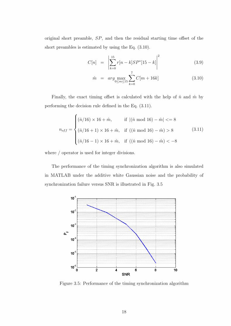
original short preamble, SP , and then the residual starting time offset of the
short preambles is estimated by using the Eq. (3.10).
C[n] =
∣∣∣∣∣15∑k=0
r[n− k]SP ∗[15− k]
∣∣∣∣∣2
(3.9)
m = arg max0≤m≤15
7∑k=0
C[m+ 16k] (3.10)
Finally, the exact timing offset is calculated with the help of n and m by
performing the decision rule defined in the Eq. (3.11).
noff =
(n/16)× 16 + m, if |(n mod 16)− m| <= 8
(n/16 + 1)× 16 + m, if ((n mod 16)− m) > 8
(n/16− 1)× 16 + m, if ((n mod 16)− m) < −8
(3.11)
where / operator is used for integer divisions.
The performance of the timing synchronization algorithm is also simulated
in MATLAB under the additive white Gaussian noise and the probability of
synchronization failure versus SNR is illustrated in Fig. 3.5
Figure 3.5: Performance of the timing synchronization algorithm
18

3.1.4 Fine Frequency Synchronization
As mentioned in Chapter 1, the carrier frequency offset due to the local oscil-
lator mismatch or a Doppler shift must be finely corrected by the receiver for
eliminating the ICI. Therefore, we used the long preambles in a same manner as
described in 3.1.2 to obtain a more accurate estimation of the frequency offset.
If the complex correlation function, defined in Eq. (3.3) is calculated for the
long preambles whose length is 64, it gives four times accurate result than the
short ones. Then, the frequency offset is finely estimated from the phase of the
correlation result, CL[n], as follows
δfL =fs∠CL[n]
2π64(3.12)
As a result, the frequency offset can be eliminated from the received signal by
multiplying it with exp(−j2πδfLn/fs) and the final estimation can be written
by combining the coarse and fine estimations as the following:
δf =⌊δfc
⌋+ δfL (3.13)
Eq. (3.12) shows that the maximum estimated frequency offset is limited by
the unambiguous region of the CL[n] phase. This means that this algorithm can
compensate a maximum frequency offset of |δfmax|L = fs/128 = 156.25 KHz if
the only long preambles are used. Since the use of the short preambles for coarse
estimation, this limit is extended up to |δfmax| = fs/2NS = 625 KHz.
3.1.5 Channel Estimation
In a wireless communication channel, the transmitted signal reaches the receiver
antenna via multiple paths with different delays and gains. Thus, the receiver
must estimate the channel response in order to coherently demodulate the re-
ceived symbols. The IEEE 802.11a standard assumes that the wireless channel
19

does not change during the transmission period of a packet. It transmits two
long preamble symbols at the beginning of each frame so that the receiver can
obtain the channel impulse response coefficients [4].
h[n] =L−1∑i=0
hi · δ[n− i] =L−1∑i=0
ai exp(jθi)δ[n− i] (3.14)
For analyzing the multi-path channel effect on the received samples, let us
consider a simple multi-path channel model with L taps as in Eq. (3.14). The
resulting received signal can be written as follows
y[n] = x[n] ? h[n] + w[n] =L−1∑i=0
hi · x[n− i] + w[n] (3.15)
where the x[n] is the transmitted signal in Eq. (1.2) and w[n] is a complex
baseband white Gaussian noise. Using the periodicity of the transmitted signal
during the long preambles, the time domain convolution in Eq. (3.15) can be
expressed by a matrix multiplication for the preamble symbols as the following
[8].
y0
y1...
y62
y63
︸ ︷︷ ︸
=
x0 x63 · · · x63−L+2
x1 x0 · · · x63−L+3
......
. . ....
x62 x61 · · · x63−L
x63 x62 · · · x63−L+1
︸ ︷︷ ︸
·
h0
h1...
hL−2
hL−1
︸ ︷︷ ︸
+
w0
w1
...
w62
w63
︸ ︷︷ ︸
Y = X · H + W
(3.16)
From this point of view, the channel impulse response vector, H, can be
estimated by using the least square (LS) estimation technique as follows
H = XH ·(X ·XH
)−1 · Y = X+ · Y (3.17)
where X+ denotes the Moore-Penrose generalized inverse of X.
The maximum delay spread of the wireless channel must be less than the
length of the CP interval for an ISI-free reception, so the length of the channel
20

impulse response vector in Eq. (3.16) is selected as being equal to the length of
the CP interval, 16. In addition, the received samples of the first and second
long preamble symbols can be averaged in order to reduce the noise variance
on the estimated channel coefficients and the Eq. (3.17) can be rewritten as the
following.
H =1
2X+ · (Y1 + Y2) (3.18)
3.1.6 Channel Equalization
After estimating the channel impulse response, the receiver must remove the
effects of the channel from the received signal. This is the task of the equalization
block which normalizes all the sub-carriers with their estimated channel transfer
function. In order to analyze the multi-path channel effect on each sub-carrier,
let us write the FFT of the received signal in Eq. (3.15).
Y [k] =N−1∑n=0
y[n] exp
(−j2πkn
N
)
=
p−1∑i=0
ai ejθiN−1∑n=0
x[n− i] exp
(−j2πkn
N
)+W [k]
=
p−1∑i=0
ai ejθiN−1∑n=0
N−1∑k=0
X[k − i] exp
(j2π
k(n− i)N
)exp
(−j2πkn
N
)+W [k]
= X[k]
p−1∑i=0
ai exp
(j
(θi − 2π
ki
N
))+W [k]
= X[k] ·H[k] +W [k] (3.19)
As a result of the Eq. (3.19), the effects of the channel on each sub-carrier can
be compensated if the receiver has a knowledge of the channel transfer function
for all sub-carrier indexes. This knowledge can be easily obtained by taking the
FFT of the channel impulse response coefficients found in Eq. (3.18). Then,
the channel equalization can be performed using a one-tap frequency domain
21

equalizer as follows
X[k] =Y [k]
H[k](3.20)
where H[k] is the estimated channel transfer function at the k’th sub-carrier.
In addition to the equalization of each sub-carrier, the receiver must also track
the carrier phase while receiving the data symbols in a packet. Because of the
fact that the frequency synchronization procedure is not a perfect process, there
will be a small residual frequency error in the equalized signal. This frequency
error causes a phase rotation on the received constellation and degrades the
system performance significantly. As described in [8], the phase rotation due to
the residual frequency error is the same for all sub-carriers and the amount of
the phase rotation at the n’th OFDM data symbol can be estimated by utilizing
the four pilot sub-carriers as follows
Φn = ∠
[ ∑k=−21,−7,7,21
Rn,k
Pn,k
](3.21)
where Rn,k is the received equalized pilot sub-carrier and Pn,k is the transmitted
pilot sub-carrier of the n’th OFDM data symbol.
After estimating the accumulated phase value, the equalized constellation
points of each OFDM data symbols are derotated by multiplying them with
exp(−jΦn).
3.2 IEEE 802.11a MATLAB Simulator
In order to observe the performance of the receiver algorithms, we firstly modelled
the IEEE802.11a transmitter in MATLAB. The IEEE 802.11a standard gives an
example of encoding a frame for the physical layer. We applied the transmitted
message defined in this example to the input of our transmitter model and con-
firmed the validity of our model by comparing its output with the time domain
waveform obtained in the standard for this example.
22

After modelling the transmitter, we designed the simulator shown in Fig. 3.6
to test our receiver solution under a multipath channel with additive white Gaus-
sian noise and Rayleigh fading statistics. Through this simulator, the perfor-
mance of the receiver can be observed under various channel conditions and for
different transmitter and receiver parameters.
Figure 3.6: Runtime snapshot of the IEEE802.11a Matlab Simulator
The first parameter on the graphical user interface (GUI) is labelled as “1.
Channel Type” and the channel model between the transmitter and receiver can
be adjusted as AWGN or dispersive fading channel at runtime via the pop-up
menu just besides this label. If the dispersive fading channel model is selected,
the number of multipath delay taps is determined by the second parameter and
the instantaneous channel impulse response can be observed on Fig. 3.6.d. In
addition, the signal to noise ratio (SNR) at the receiver input can be set using the
23
slider bar labelled as “3. Input SNR:” and the simulator reports the estimated
SNR of the equalized received signal on Fig. 3.6.h.
The fifth parameter on the GUI creates a deviation between the transmitter
and receiver local oscillators and the performance of the frequency estimation
algorithm is displayed on Fig. 3.6.k. The decision type of the Viterbi decoding
algorithm can also be adjusted as hard or soft decision via the pop-op menu
associated with the label “Viterbi Decision Type”. Apart from these, the user
can also observe the effects of the power amplifier distortion on the IEEE802.11a
link. The simulator enables the user to select power amplifier model as linear,
clipping or non-linear Saleh Model [9] and to adjust the input back-off factor
of the amplifier. Besides, the simulator also displays the power spectrum of the
transmitted signal on Fig. 3.6.e to demonstrate the distortions on the spectrum
caused by the non-linear power amplifier. In order to suppress the out of band
radiations, the windowing technique proposed in the standard [4] can be applied
on the transmitted signal by smoothing the transitions between the OFDM sym-
bols. The last parameters on the GUI select the windowing function and adjust
the smoothing duration.
24

Chapter 4
FPGA IMPLEMENTATION
We implemented the IEEE 802.11a transceiver on the Lyrtech Small Form Factor
(SFF) Software Defined Radio (SDR) Development Platform which is described
in Appendix A. The receive path of the Lyrtech RF module down-converts the
received signal to an intermediate frequency at 30 MHz. This means that the
received IEEE802.11a signal at the input of ADC has a maximum frequency of
40 MHz and so the minimum sampling rate should be 80 MHz in accordance with
the Shannon-Nyquist criteria. If the received signal is sampled at 80 MHz, a very
sharp low-pass filter is required at the base-band conversion stage to suppress
the mirror images of the digital signal. For this reason, the sampling rate of the
ADC and the system clock rate of the FPGA were selected as 120 MHz.
We used the System Generator tool of Xilinx to develop the FPGA imple-
mentation of the transceiver. This tool facilitates the FPGA hardware design for
Digital Signal Processing (DSP) and extends the MATLAB Simulink to provide
a high level development environment for Xilinx FPGAs [10]. We firstly designed
the system models of the transmitter and receiver in the Simulink environment
using the Xilinx library which includes the bit-accurate models for the circuit
25

blocks in the FPGA. Then, we obtained the HDL codes for our models which
are automatically created by the System Generator.
In this chapter, the system generator implementation of the IEEE802.11a
transmitter and receiver architectures will be explained in detail. In addition,
the measured bit error rate (BER) performance of the receiver under an Additive
White Gaussian Noise (AWGN) channel will be submitted at the end of the
chapter.
4.1 Transmitter Implementation
Figure 4.1: System Generator model of the transmitter
The system generator implementation of the transmitter is divided into five
subsystems as shown in the Fig. 4.1. The first subsystem which is named as
processControl is designed for controlling the signal flow from the MAC layer to
the DAC. The second subsystem is used to implement the bit based operations,
such as convolutional encoding and interleaving. Then, the CarrierModulation
subsystem converts the interleaved bits into the complex constellation symbols
and the CyclicIFFT subsystem takes the inverse Fourier transforms of these
symbols to generate the time domain base-band signal. Finally, the Interpolation
block synchronizes the IFFT output with the DAC operating at 120 MHz. In the
26

following subsections, the implementation of each subsystem will be explained in
detail.
4.1.1 Subsystem 1: ProcessControl
The interface of the physical layer with the MAC layer is provided by the Pro-
cessControl subsystem. The MAC layer adjusts the data rate and the number
of the bytes in the frame, which will be transmitted, though the “mode” and
“nOfBytes” inputs, respectively. After that, it starts the transmission by driving
the “txStr” input to logic high and writes the bytes for the current frame into
the input buffer of the transmitter.
Figure 4.2: Timing diagram of the transmitter pipeline structure
After triggering from the “txStr” input, the ProcessControl subsystem calcu-
lates the number of OFDM symbols required for the current frame and generates
the symbol start, “sStr”, and symbol type signals, “sType”, to control the signal
flow through all the subsystems in the transmitter. In addition, this block also
produces the signal field and scrambled OFDM data bits by reading the bytes
in the input buffer. As illustrated in Fig. 4.2, the ProcessControl block pro-
duces the raw bits for only one OFDM symbol per 480 clock cycles and the other
subsystems processes these bits in a pipelined manner to produce the baseband
in-phase and quadrature signals.
27

4.1.2 Subsystem 2: FecAndInterleaver
Fig. 4.3 shows the implementation architecture of the FecAndInterleaver subsys-
tem. Firstly, the incoming bits from the ProcessControl subsystem are encoded
by the ConvEncoder block which produces two bits output for every one bit in-
put. Then, the produced bits are stored in a dual port block memory. At the
next pipeline interval, the stored bits of the previous OFDM symbol are read
in an order which is determined by the interleaver permutations and puncturing
codes defined in the IEEE802.11a standard. However, a different read order must
be generated for each modulation type and FEC rate combination. In order to
simplify the implementation, the read addresses of the interleaved and punctured
bits are kept in a ROM. In this way, the subsystem only generates the sequential
address pointers for the read address ROM. Then, the output of this ROM is
used for reading the desired bits from the block memory.
Figure 4.3: Implementation of the FecAndInterleaver subsystem
4.1.3 Subsystem 3: CarrierModulation
The CarrierModulation subsystem captures the serial bits produced by the Fe-
cAndInterleaver block and divides them into groups of 1, 2, 4 or 6 bits according
to the modulation type: BPSK, QPSK, 16-QAM or 64-QAM, respectively. Then,
28

it converts the produced groups into the complex signals representing the con-
stellation points as shown in Table 4.1 to 4.3. Considering all the modulation
type, there are 16 different in-phase and 15 different quadrature components of
the constellations. As a consequence of that, the CarrierModulation subsystem
keeps all the constellation points in two look up tables (LUT), one for in-phase
and one for quadrature component, and addresses the LUTs by using the pro-
duced bit groups and the modulation type input to generate the constellation
symbols.
BPSK Modulation QPSK Modulation
Bit:b0 In-Phase Quadrature Bit:b0 In-Phase Bit:b1 Quadrature
0 -1 0 0 −1/√
2 0 −1/√
2
1 +1 0 1 +1/√
2 1 +1/√
2
Table 4.1: BPSK and QPSK modulation IQ mapping
Bits (b0:b1) In-Phase Bits (b2:b3) Quadrature
00 −3/√
10 00 −3/√
10
01 −1/√
10 01 −1/√
10
11 +1/√
10 11 +1/√
10
10 +3/√
10 10 +3/√
10
Table 4.2: 16 QAM modulation IQ mapping
Bits (b0:b1:b2) In-Phase Bits (b3:b4:b5) Quadrature
000 −7/√
42 000 −7/√
42
001 −5/√
42 001 −5/√
42
011 −3/√
42 011 −3/√
42
010 −1/√
42 010 −1/√
42
110 +1/√
42 110 +1/√
42
111 +3/√
42 111 +3/√
42
101 +5/√
42 101 +5/√
42
100 +7/√
42 100 +7/√
42
Table 4.3: 64 QAM modulation IQ mapping
As shown in Fig. 4.4, the CarrierModulation subsystem stores the generated
constellation symbols in a buffer. At the next process interval, the stored symbols
are read in a shifted order, as described in Section 2.3.4, and the pilot sub-carriers
29

are inserted at appropriate positions. In order to interpolate the transmitted sig-
nal, the CarrierModulation block also extends the Fourier transformation input
sequence to 256 points by zero padding. Besides, at the beginning of each frame,
this subsystem sends the preamble sequences stored in a ROM to the IFFT block
by multiplexing the output.
Figure 4.4: Carrier Modulation subsystem
4.1.4 Subsystem 4: CyclicIFFT
The cyclicIFFT subsystem takes the IFFT of the frequency domain sub-carrier
symbols for generating the time domain baseband signal. The IFFT size is
selected as 256 to interpolate the output signal with four times. For the FPGA
implementation of the 256 point IFFT in a pipelined manner, we used the Radix-
22 Single Delay Feedback (SDF) algorithm proposed by He and Torkelson. The
complexity of this algorithm in terms of the number of complex multiplication is
the same as the Radix-4 IFFT algorithm but it preserves the butterfly structure
of the radix-2 algorithm in order to reduce the number of additions. For a N-point
IFFT operation, the Radix-22 SDF algorithm uses log4N −1 complex multiplier,
4 log4N complex addition and N − 1 complex data memory [11].
x[n] =N−1∑k=0
X[k] ·W knN 0 ≤ n < N (4.1)
30

The Radix-22 SDF algorithm decimates the output samples of N-point IFFT,
defined as in Eq. (4.1), by a factor of four. Then, it combines the common twiddle
factors and simplifies the equation as the following.
x[4n+ 2n2 + n1] =
N/4−1∑k=0
1∑k1=0
1∑k2=0
X[k + k1N
2+ k2
N
4] ·W (4n+2n2+n1)(k+k1
N2+k2
N4)
N
=
N/4−1∑k=0
1∑k2=0
B[k + k2N/4, n1] ·W (k+k2N/4)n1
N ·W (n2+2n)(k+k2N/4)N/2
=
N/4−1∑k=0
(B[k, n1] + j2n2+n1B[k +N/4, n1]
)·W k(2n2+n1)
N ·W knN/4 (4.2)
where, B[k, n1] = X[k] + (−1)n1 +X[k +N/2] and n1 = {0,1}, n2 = {0,1}.
According to the Eq. (4.2), a N-point IFFT of a sequence can be easily cal-
culated by using a N/4 point IFFT after performing the butterfly and complex
multiplication operations as illustrated in Fig. 4.5. From this point of view, a
256 point IFFT can be taken in four stages, where each stage involves two but-
terfly structures and one complex multiplication. The multiplication at the last
stage is trivial, so it can be eliminated and only three complex multiplications
are needed for performing the inverse Fourier transformation.
Figure 4.5: Radix-22 SDF butterfly structure for 16 point IFFT
31

Fig. 4.6 shows the system generator implementation of the first butterfly
in the first stage. The butterfly architecture needs the first 128 samples to
calculate the outputs, so a block ram is used to provide a delay of 128 samples.
While receiving the last half of the input sequence, the implementation adds the
incoming sample with the delayed one and sends the result to the output. In the
same time, it also subtracts the input samples from the delayed one and writes
the result to the delay buffer. At the next processing interval, the subtraction
results are read from the buffer and directed to the output while buffering the
first half of the next sequence. The pipeline process is carried out in this manner.
Figure 4.6: Fpga implementation of the Butterfly 1 in Stage 1
The implementation of the second butterfly is similar to the first one, except
the trivial multiplication by j. The output of the second butterfly is multiplied
with the twiddle factors in a ROM by a complex multiplier. As shown in Fig. 4.7,
the complex multiplier is implemented by cascading four DSP48 slices to perform
four real multiplications and two additions without using any external resources.
32

Figure 4.7: Complex multiplier implementation with cascaded DSP48 slices
The time domain samples are obtained in a bit reverse order from the output
of the last IFFT stage, so the output samples of the IFFT block are buffered in
a RAM for reordering. After completing the Fourier transformation, the calcu-
lated samples are read from the buffer in a cyclic manner and multiplied with a
windowing function, illustrated in Fig. 4.8, in order to suppress the out of band
radiations. The windowing function is stored in a block memory and can be
updated by the MAC layer to change the smoothing duration, TW .
Figure 4.8: Illustration of the OFDM symbol windowing
In addition to these, the designed IFFT core was also compared with the
available Xilinx IFFT core in terms of the FPGA resource utilization. As shown
in Table 4.4, our implementation uses the FPGA slices 29% more efficiently than
the Xilinx core.
33
Resources Xilinx IFFT Core Our IFFT Core
Slice 1897 1343Flip-Flop 2847 1716
Look Up Table 2797 2306Block RAM 3 3
DSP48 Multiplier 12 12
Table 4.4: Resource comparison of the IFFT cores
4.1.5 Subsystem 5: Interpolation
The output rate of the CyclicIFFT subsystem is equal to 80 Msps, whereas the
operating clock frequency of DAC is 120 MHz. For this reason, the Interpolation
subsystem is designed to interpolate the received samples from the CyclicIFFT
block by a factor of 3/2. In order to perform the interpolation by 3/2, the input
signal is firstly upsampled by inserting two zeros between the input samples.
Then, the produced signal is filtered by a low pass filter and downsampled by a
factor of two as shown in Fig. 4.9. However, there is no need to implement all the
interpolation steps, only the calculation of the used samples by the downsampler
can be considered.
Figure 4.9: Block diagram for the interpolation by 3/2
If it is assumed that the down-sampling block selects the even samples of the
input signal, the output of the interpolation, y[n], can be expressed as
y[n] = s[2n] = v[2n] ? h[2n] =L−1∑k=0
h[k] · v[2n− k] (4.3)
34

The Eq. (4.3) can also be simplified as the following by considering only the
non-zero samples of v[n].
y[3n+ l] =
∑L/3−1k=0 h[3k] · x[2n− k] when l = 0∑L/3−1k=0 h[3k + 2] · x[2n− k], when l = 1∑L/3−1k=0 h[3k + 1] · x[2n+ 1− k], otherwise
(4.4)
As a result of the Eq. (4.4), the designed interpolation FIR filter with 18
coefficients is implemented by using a sixth order FIR filter. The filter coefficients
are switched in accordance with the interpolation time index and the filter output
is calculated by cascading six DSP48 slices as illustrated in Fig. 4.10.
Figure 4.10: Interpolation filter implementation
4.2 Receiver Implementation
The system generator implementation of the receiver is divided into nine subsys-
tems as shown in Fig. 4.11. The first subsystem, named as “DownConverter”,
converts the IF signal received from the ADC into base-band I and Q components
by a quadrature detector and decimates the output by a factor of six to produce
a 20 MHz output sample rate. Then, the frame detection, timing and frequency
35

Figure 4.11: System Generator model of the receiver
36

synchronization processes are performed by the “preambleDecode” subsystem
as described in Section 3.1. Next, the “chanEstimation” subsystem estimates
the channel impulse response coefficients in time domain and removes the cyclic
prefix from the received samples. The 64 point FFT of the remaining samples
and channel impulse response coefficients are taken by the “FFT64” subsystem,
which is implemented in a similar way as explained in Subsection 4.1.4. After
obtaining the frequency domain subcarrier symbols, the “channelEqualizer” sub-
system performs the channel equalization and carrier phase tracking algorithms
described in Subsection 3.1.6. Then, the “subCarrierDemod” subsystem com-
putes the log likelihood ratios (LLR) of the received bits by demodulating the
equalized constellation symbols. In addition, it also rearranges the order of the
LLRs by a reverse operation of the interleaving at the transmitter and sends
them to the “viterbiDecoder” subsystem to decode the bitstream that has been
convolutionally encoded. Finally, the decoded bits, except for the signal field,
are fed to the “deScrambler” subsystem to reconstruct the transmitted message.
The decoded bits of the Signal Field are also sent to the “signalParsing” block to
extract the frame parameters such as modulation type, number of transmitted
bytes and the number of OFDM symbols in the frame.
In the following subsections, the implementation of the receiver subsystems
that are dissimilar to the transmitter counterparts will be explained in detail.
4.2.1 Down Conversion to Baseband
The down conversion of the IF signal received from the ADC into the baseband
I&Q components is illustrated in Fig. 4.12. The carrier frequency of the received
signal is 30 MHz and the system clock frequency is equal to 120 MHz, so the
cosine and sine components of the local oscillator can be easily generated by
repeating the {1,0,-1,0} sequence.
37
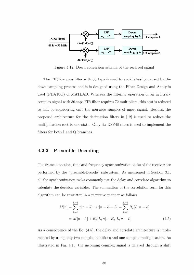
Figure 4.12: Down conversion schema of the received signal
The FIR low pass filter with 36 taps is used to avoid aliasing caused by the
down sampling process and it is designed using the Filter Design and Analysis
Tool (FDATool) of MATLAB. Whereas the filtering operation of an arbitrary
complex signal with 36-taps FIR filter requires 72 multipliers, this cost is reduced
to half by considering only the non-zero samples of input signal. Besides, the
proposed architecture for the decimation filters in [12] is used to reduce the
multiplication cost to one-sixth. Only six DSP48 slices is used to implement the
filters for both I and Q branches.
4.2.2 Preamble Decoding
The frame detection, time and frequency synchronization tasks of the receiver are
performed by the “preambleDecode” subsystem. As mentioned in Section 3.1,
all the synchronization tasks commonly use the delay and correlate algorithm to
calculate the decision variables. The summation of the correlation term for this
algorithm can be rewritten in a recursive manner as follows
M [n] =L−1∑k=0
x[n− k] · x∗[n− k − L] =L−1∑k=0
Rx[L, n− k]
= M [n− 1] +Rx[L, n]−Rx[L, n− L] (4.5)
As a consequence of the Eq. (4.5), the delay and correlate architecture is imple-
mented by using only two complex additions and one complex multiplication. As
illustrated in Fig. 4.13, the incoming complex signal is delayed through a shift
38

register and the correlation term is calculated by a DSP48 based complex multi-
plier. Then, the difference between the output of the multiplier with the delayed
version of it is obtained using a subtraction block and the result is accumulated
to form the decision variable.
Figure 4.13: Implementation of the delay and correlation algorithm
Apart from the delay and correlate method, the timing synchronization al-
gorithm also uses the cross-correlation between the received signal and the orig-
inal short preamble symbol. The calculation of the cross-correlation function
in Eq. (3.9) requires 16 complex multiplications. However, as shown in Table
4.5, the imaginary part of the short preamble symbol is a circularly shifted ver-
sion of its real part and this property can be used to reduce the implementation
complexity.
k Real(SP[k]) Imag(SP[k]) k Real(SP[k]) Imag(SP[k])
0 0.1250 0.1250 8 0.1250 0.12501 -0.3599 0.0064 9 0.0064 -0.35992 -0.0366 -0.2134 10 -0.2134 -0.03663 0.3879 -0.0344 11 -0.0344 0.38794 0.2500 0.0 12 0.0 0.25005 0.3879 -0.0344 13 -0.0344 0.38796 -0.0366 -0.2134 14 -0.2134 -0.03667 -0.3599 0.0064 15 0.0064 -0.3599
Table 4.5: One period of the short preamble sequence
If the summation in Eq. (3.9) is divided into two parts, the cross-correlation
operation can be performed by using two FIR filters with real-valued coefficients
39

as the following:
Rrs[n] =15∑k=0
r[n− k]SP ∗[15− k]
=7∑
k=0
r[n− k]SP ∗[15− k] +7∑
k=0
r[n− k − 8]SP ∗[7− k]
=7∑
k=0
r[n− k] · (h2[k]− jh1[k]) +7∑
k=0
r[n− k − 8] · (h1[k]− jh2[k])
= (r[n]− jr[n− 8]) ? h2[n] + (r[n− 8]− jr[n]) ? h1[n] (4.6)
Moreover, we adapted the symmetric systolic FIR filter architecture proposed
in [12] to implement the h1[n] and h2[n] filters. As illustrated in Fig. 4.14, the
required number of multipliers for h1[n] is halved by adding the input samples
before being multiplied by the same coefficient. The single multiplications by
0.25 and 0.125 are accomplished by simply shifting the binary decimal point
to the right and the remaining fractional multiplications are implemented using
embedded multipliers.
Figure 4.14: Implementation of the correlation filter, h1[n]
In the implementation of the frequency synchronization algorithm, Xilinx
Coordinate Rotational Digital Computer (CORDIC) core ([13]) is used to find
the phase of the correlation result in Eq. (3.12). After estimating the frequency
offset from the phase value, the desired complex sinusoid is generated by using a
Direct Digital Synthesizer (DDS) core of Xilinx [14]. Then, the frequency offset is
eliminated by multiplying the input signal with the generated complex sinusoid.
40

4.2.3 Channel Estimation
The “chanEstimation” subsystem in Fig. 4.11 estimates the channel impulse
response coefficients as described in Subsection 3.1.5. The FPGA implementation
block schema of the “chanEstimation” subsystem is illustrated in Fig. 4.15. This
subsystem firstly calculates the average of the frequency corrected long preamble
symbols and stores the result samples into a block RAM based buffer. After
receiving all the samples of the long preamble symbols, the subsystem reads the
preamble samples from this buffer and the generalized inverse of X in Eq. (3.18)
from a ROM and performs the complex matrix multiplication operation.
Figure 4.15: Block schema of the chanEstimation subsystem
The complex multiply and accumulate unit in Fig. 4.15 includes two paral-
lel complex multiplier and completes the matrix operation in 512 clock cycles.
Then, the calculated channel coefficients are send to the FFT block to obtain
the channel transfer function for all sub-carriers. In addition to the estimation of
channel coefficients, this subsystems removes the cyclic prefix interval from the
received samples and sends the remaining samples of the OFDM data symbols
to the FFT block by multiplexing the output. Due to the execution latency of
the matrix operation, the received samples must be delayed before sending to
the FFT block.
41

4.2.4 Channel Equalizer
Fig. 4.16 shows the system generator implementation of the “channelEqualizer”
subsystem which performs the channel equalization process by evaluating the
complex division operation in Eq. (3.20). This division operation is made in two
steps, first the inverse (under multiplication) of the channel frequency response
coefficients is calculated as follows,
1
H[k]=
H[k]∗
H[k] · H[k]∗(4.7)
then the calculated values are multiplied with the incoming sub-carrier symbols
from the FFT subsystem.
Figure 4.16: Channel Equalization subsystem
The “inverseCalculation” block is designed for implementing the division op-
eration in Eq. (4.7). This block firstly calculates the absolute square of the
42

channel frequency response coefficients by multiplying them with complex con-
jugate versions and the absolute square result is expressed by 32 bits. In order
to simplify the inverse calculation of this result, it is truncated by taking the
most meaningful 12 bits. For this purpose, the block finds the position of first
non-zero bit of the result from the most significant side and takes the consecutive
12 bits from this position to the least significant side. Then, these bits are used
to address a block RAM based look-up table which holds the inverse (under mul-
tiplication) values. Finally, the obtained values are multiplied by the conjugate
of the frequency response coefficients to get the inverse under multiplication of
these coefficients. However, due to the scaling during the truncation operation,
the outputs of this block are transfered to the next blocks with a scale factor.
The channel frequency response coefficients are obtained from the “FFT64”
subsystem and captured by the “channelEstBuffer” block. This block sends the
captured coefficients to the “inverseCalculation” block to perform the division
operation and stores the division results with the scale factors in a block RAM.
While processing the OFDM symbols followed by the preambles, the inverse of
the channel frequency response estimates and the incoming symbols are trans-
mitted to the “longPreambleEqualizer” block. In this block, the preamble based
channel equalization procedure is completed by performing the complex multi-
plication of the input samples and compensating the effect of the scale factor.
In addition to the equalization of each sub-carrier, the “channelEqualizer”
subsystem also estimates the accumulated carrier phase value of each OFDM
data symbols as given in Eq. (3.21) and de-rotates the equalized constellation
symbols according to this value. The estimation of the carrier phase values is
made by the “phaseEstimation” block which adds the symbols at the pilot sub-
carriers after correcting the polarities of them. Then, the phase of this summation
must be found and an exponential signal whose phase is the negative of the es-
timated value must be generated to perform the de-rotation. Instead of using
43

a CORDIC and a Sin-Cosine Generator cores to implement these operations in
hardware, the exponential de-rotation signal can be obtained by normalizing the
amplitude of the pilot summation and conjugating the result. For this purpose,
the “phaseEstimation” block sends the summation result to the “inverseCalcu-
lation” block. In this case, the inverse of the input signal is calculated by this
block as follows
P [n]∗√P [n]∗ · P [n]
= exp(−j · ∠P [n]
)(4.8)
where P [n] is the summation of the pilot subcarriers for the n’th OFDM symbol.
After generating the exponential de-rotation signal, the “pilotPhaseTracking”
block performs the de-rotation by multiplying the equalized constellation symbols
with this exponential.
4.2.5 Subcarrier Demodulation
The “subCarrierDemod” subsystem demodulates the equalized constellation
symbols and obtains the log likelihood ratios of the received bits which will
be used by the soft decision Viterbi decoder. For BPSK and QPSK modulation
types, the LLR of each bit can be easily calculated by evaluating only the in-phase
or quadrature components of the constellation symbols. However, the calcula-
tion of LLR is more difficult for the 16-QAM and 64-QAM modulation types (see
Tables 4.2 and 4.3), because each component of the constellation carries two and
three bits of information, respectively.
We used the simplified log likelihood ratio method proposed by Tosato and
Bisaglia [15] to obtain the soft decision information. The calculation of LLRs
associated with the bits carried over the in-phase component is given in the
following equations. These equations, except for the BPSK, are also used to cal-
culate the ratios of the bits on the imaginary axis by substituting the quadrature
44

component of the constellation symbol into the equations.
BPSK : LLR(b0) = [yI [n]× 32] (4.9)
QPSK : LLR(b0) =[yI [n]×
√2× 32
](4.10)
16QAM :LLR(b0) =[yI [n]×
√10÷ 3× 40
]LLR(b1) =
[(2−
∣∣∣yI [n]×√
10∣∣∣)÷ 3× 40
](4.11)
64QAM :LLR(b0) =[yI [n]×
√42÷ 7× 48
]LLR(b1) =
[(4−
∣∣∣yI [n]×√
42∣∣∣)÷ 7× 48
]LLR(b2) =
[(2−
∣∣∣4− ∣∣∣yI [n]×√
42∣∣∣∣∣∣)÷ 7× 48
](4.12)
where [·] operator denotes the rounding to the closest integer.
In order to perform the reverse operations of the interleaving and punctur-
ing at the transmitter, the “subCarrierDemod” subsystem stores the LLRs of
the currently decoded OFDM symbol in a block RAM. At the next symbol de-
coding interval, this subsystem reads the stored LLRs from the memory in a
de-interleaved and de-punctured order and sends them to the Viterbi algorithm
processor.
4.2.6 Viterbi Decoder
The IEEE802.11a receiver uses the Viterbi algorithm to decode the convolu-
tionally encoded forward error correction codes. The Viterbi algorithm is com-
monly represented by a trellis diagram, which shows the state transitions in a
time indexed manner. A simple trellis diagram with four states is illustrated
in Fig. 4.17a. There are two outgoing branches for each state at a given time
instant, one corresponds to the encoder input bit of zero and the other corre-
sponds to an input bit of one. The algorithm first calculates the probabilities
of each outgoing branches, named as branch metric, and accumulates them onto
the path (state) metrics of the previous time instant. Due to the existence of
45

two incoming paths for each state, the algorithm selects the one with a bigger
metric and records the selected one as a survivor path. Finally, after processing
all the input data in a frame, the decoded output sequence is obtained by tracing
backward the most probable path [16].
(a) (b)
Figure 4.17: (a)Trellis diagram of the Viterbi decoder, (b) butterfly structure
The system generator implementation of the Viterbi decoder consists of three
units as shown in Fig. 4.18. The Branch Metric Unit (BMU) calculates the
metrics for only “11” and “10” branches by adding and subtracting the incoming
LLRs, respectively. There is no need to calculate the other metrics because they
are equal to the negative of the calculated ones.
Figure 4.18: System Generator block diagram of the Viterbi decoder
The convolutional encoder used in the IEEE802.11a standard has a delay line
with six registers, so the number of states in the trellis diagram is equal to 26.
To provide a simplicity in the implementation, these states are rearranged in 32
46

butterfly structures as illustrated in Fig. 4.17b for four states. The Path Metric
Unit (PMU) of the Viterbi decoder uses one Add-Compare-Select (ACS) unit,
shown in Fig. 4.19, for each butterfly to calculate the new values of path metrics
and determine the survivor paths.
Figure 4.19: Block diagram of butterfly Add-Compare-Select unit
In the implementation of the ACS unit with finite precision arithmetic, we
used the modulo normalization technique proposed in [17] in order to avoid over-
flow problems of the recursively calculated path metrics. According to this tech-
nique, the range of the path metric register must be greater than two times the
maximum possible difference between the path metrics. In our receiver design,
the differences between the metrics are less than 1024 for the LLRs expressed
with seven bits. Therefore, the width of the path metric registers was adjusted
as 11 bits.
The last block in the Viterbi decoder is the Trace Back Unit which is im-
plemented as proposed in [18]. This unit stores the incoming 64 survivor paths
generated by the PMU in one of four block RAMs as illustrated in Fig. 4.20.
While storing the survivors of the n’th block, the previously stored block (n-1)
is traced back in order to determine the starting state of the block n-2. At the
same time, the output bits for the block n-3 are collected by tracing backward the
associated block and stored in a shift register. At next block processing interval,
the decoded bits are read from the shift register in a reverse order and directed
to the output. The pipelined decoding process is continued in this manner.
47

Figure 4.20: Timing diagram of the trace back memory access
4.3 Performance Measurements
In order to test our IEEE802.11a physical layer prototype on the Lyrtech SFF
SDR Development Platform, we also developed a simple MAC layer running on
the platform and an user interface program on the PC. This structure enables
the user to observe the performance of the transceiver under a wireless link con-
structed between two Lyrtech platforms or under an AWGN channel which is
modelled in baseband. As shown in Fig. 4.21, all the modem operating parame-
ters and the RF/IF settings of the platform can be adjusted by the user interface
program which connects to the platform through the Ethernet. Because of fact
that the RF modules on the platform can operate in a frequency range from
262 MHz to 876 MHz (Appendix A), we tested our prototype in this frequency
range instead of in true scenario at 5 GHz.
Figure 4.21: Snapshot of the User Interface Program
48

In the Constellation Test tab of the user program, the constellation of the
received signal is monitored at runtime as illustrated in Fig. 4.22 and 4.23. In this
mode, the MAC layer collects the equalized or unequalized constellation samples
from the receiver and sends them to the PC through an Ethernet packet.
(a) (b)
Figure 4.22: Runtime snapshot of (a)BPSK and (b)QPSK constellations
(a) (b)
Figure 4.23: Runtime snapshot of (a)16-QAM and (b)64-QAM constellations
In addition to constellation monitoring, the MAC layer also measures the bit
error rate (BER) performance of the receiver. It generates a pseudo random
binary sequence using a linear feedback shift register (LFSR) for the transmitter
and sends the generated baseband signal to the RF transmitter or performs a
49

digital loopback test under the AWGN channel model. Then, it produces the
BER statistic by comparing the received bits with a synchronized sequence to the
transmitted ones and reports the statistic results to the user interface program
as shown in Fig. 4.24.
Figure 4.24: Runtime snapshot of bit error rate measurement
By using the user interface program, we measured the BER performance of
our prototype for the QPSK, 16-QAM and 64-QAM modulation types. The
obtained BER curves are depicted in Figs. 4.25 to 4.27 for these modulation
types with the associated coding rates.
Figure 4.25: BER performance of QPSK modulation
50

We also measured the performance of the transceiver by disabling the error
correction codes and compared the obtained BER curve with the theoretical
upper bound for the corresponding modulation type.
Figure 4.26: BER performance of 16-QAM modulation
Figure 4.27: BER performance of 64-QAM modulation
51

Chapter 5
CONCLUSION AND FUTURE
WORK
The Orthogonal Frequency Division Multiplexing (OFDM) is one of the most
promising transmission technique from among the existing technologies due to
its unique features. This thesis begins with a brief overview on the advantages
and disadvantages of the OFDM systems and aims to implement the physical
layer of the IEEE802.11a Wireless LAN standard, which is one of the OFDM
based IEEE standard, on the Field Programmable Gate Arrays. Before starting
the implementation, the overall IEEE802.11a system has been modelled and
simulated in MATLAB environment. According to the simulations, the receiver
has been developed in such a way that it is more reliable and easily implemented.
The timing and frequency synchronization problems of the OFDM technique have
been exclusively considered to yield a good performance. In order to overcome
the PAPR problem of the system, the amplifier at the transmitter is operated in
its linear region and the digital signal sent to the DAC is clipped if the power of
the signal exceeds the maximum permitted limit.
52

This thesis presents an optimized FPGA implementation of the IEEE802.11a
physical layer on the Xilinx Virtex-4 sx35 chip. The high precision implemen-
tation of the transceiver utilizes 5986 slices, 45 block RAMs and 73 multipliers
of the FPGA logic resources corresponding to % 39 of sx35 chip. The trans-
mitter and receiver FPGA cores, which support all the data rates defined in
the standard, have been designed using the Xilinx “System Generator” Toolbox
for Simulink. This implementation environment enables development of high
performance DSP systems and provides automatic HDL code generation.
In addition to the low resource utilization, the bit error rate (BER) perfor-
mances of the designed FPGA implementation are quite close to the theoretical
upper limits of the modulation types QPSK, 16-QAM and 64-QAM. The differ-
ence between the measured and theoretical BER curves of the QPSK modulation
is approximately 0.4 dB. The reason of this degradation is the imperfectness of
the frequency synchronization, channel estimation and the channel equalization
tasks of the receiver. Besides, the degradation of the QAM modulations is a
little more than the QPSK because the QAM modulation type is more sensitive
to the phase error on the constellation.
As a future work, the error correction coding of the system can be improved by
using an advanced coding technique, such as Low Density Parity Check (LDPC)
or Turbo coding, but this improvement will be out of the standard. In addi-
tion, the accuracy of channel estimation can be improved using a more complex
estimation technique to make the system more resistant to fading and Doppler
effects. For this purpose, the number of pilot sub-carriers and their arrangements
can also be modified to obtain a relative good system performance. Apart from
these, the proposed PAPR reduction algorithms in [19] can be applied to the
transmitter core in order to use the power amplifier more efficiently.
53
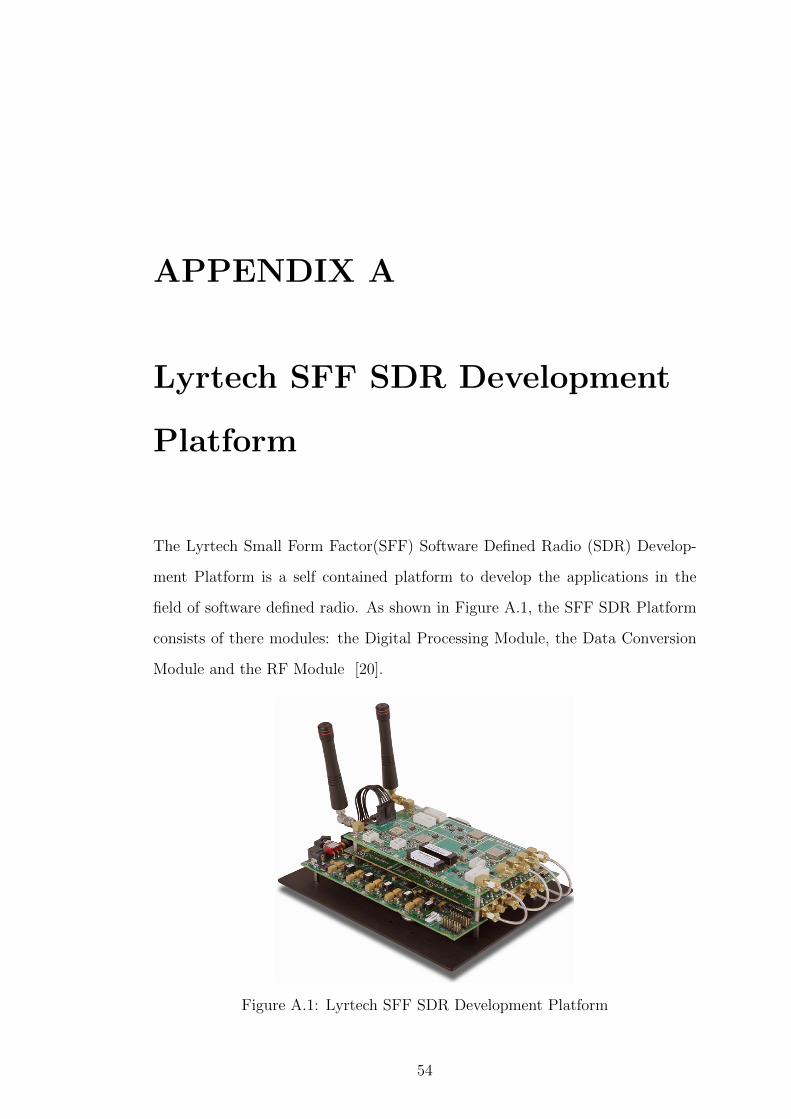
APPENDIX A
Lyrtech SFF SDR Development
Platform
The Lyrtech Small Form Factor(SFF) Software Defined Radio (SDR) Develop-
ment Platform is a self contained platform to develop the applications in the
field of software defined radio. As shown in Figure A.1, the SFF SDR Platform
consists of there modules: the Digital Processing Module, the Data Conversion
Module and the RF Module [20].
Figure A.1: Lyrtech SFF SDR Development Platform
54

The digital processing module is equipped with one Texas Instruments
TMS320DM6446 Digital Media Processor (DMP) System on Chip (SoC) and
one Virtex-4 XC4SX35 FPGA from Xilinx. The DMP SoC is a dual-core device
with a C64+ DSP and an ARM9 General Purpose Processor (GPP). All the
peripherals on the module, such as DDR2 SDRAM, USB ports, audio codec and
Ethernet Interface, are controlled by the DMP SoC. It also uses the FPGA as
a co-processor for digital signal processing tasks. This module is connected to
the Data Conversion Module through the expansion connector accessed by the
FPGA.
Figure A.2: Block diagram of the Data Conversion module
The Data Conversion Module provides the interface between the digital pro-
cessing module and the analog RF module of the platform. As shown in Fig-
ure A.2, this module is equipped with two 14-bit 125MSPS ADCs and one dual-
channel 16-bit 500 MSPS interpolating DAC to support large data-intensive ap-
plications. The module also includes a PLL for generating the sampling clock
signal and a Virtex-4 FPGA for preprocessing the incoming data and controlling
the interface with the digital processing module.
The wireless interface of the Lyrtech development platform is provided by the
RF Module which covers various frequency ranges for transmission and reception.
55

Figure A.3: Direct Quadrature RF Transmitter
The transmitting section of the RF module takes the in-phase and quadrature
signal components from the conversion module. Then, it mixes them with a
local oscillator whose frequency range from 262 MHz to 876 MHz as illustrated
in Figure A.3. The receive section of the RF module is realized with a three-stage
super heterodyne receiver. As in Figure A.4, this receiver architecture takes the
RF signal from the antenna and down converts it to an intermediate frequency
(IF) at 30 MHz.
Figure A.4: Super Heterodyne RF Receiver
56

Bibliography
[1] J. G. Andrews, A. Grosh and R. Muhamed, Fundamentals of WiMAX: Un-
derstanding Broadband Wireless Networking. Prentice Hall, 2007.
[2] R. Prasad, OFDM for Wireless Communications Systems. Boston: Artech
House, 2004.
[3] C. L. Henrik Schulze, Theory and Applications of OFDM and CDMA. John
Wiley & Sons Ltd, 2005.
[4] IEEE, “Supplement to Standard 802 Part 11: Wireless LAN Medium Access
Control (MAC) and Physical Layer (PHY) Specifications,” 1999.
[5] M. Engels, Wireless OFDM Systems: How to Make Them Work? Springer,
2002.
[6] T. M. Schmidl and D. C. Cox, “Robust frequency and timing synchoroniza-
tion for OFDM,” IEEE Transactions on Communications, vol. 45, no. 12,
1997.
[7] P. H. Moose, “A Technique for Orthogonal Frequency Division Multiplex-
ing Frequency Offset Correction,” IEEE Transactions on Communications,
vol. 42, no. 10, 1994.
[8] J. Heiskala and J. Terry, OFDM Wireless LANs: A Theoretical and Practical
Guide. Sams Publishing, 2002.
57
[9] S. Meza, M. O’Droma, Y. Lei, and A. Goacher, “Some New Memory-
less Behavioural Models of Wireless Transmitter Solid State Power Ampli-
fiers,” IEEE International Conference on Automation, Quality and Testing,
Robotics, May 2008.
[10] Xilinx Inc., “System Generator for DSP User Guide.” http:
//www.xilinx.com/support/documentation/sw_manuals/xilinx12_
1/sysgen_user.pdf, April 2010.
[11] S. He and M. Torkelson, “A New Approach to Pipeline FFT Processor,”
10th International Parallel Processing Symposium, pp. 766–770, 1996.
[12] Xilinx Inc., “XtremeDSP for Virtex-4 FPGAs User Guide.” http:
//www.xilinx.com/support/documentation/user_guides/ug073.pdf,
May 2008.
[13] Xilinx Inc., “Logicore IP Cordic v4.0 Product Specification.”
http://www.xilinx.com/support/documentation/ip_documentation/
cordic_ds249.pdf, April 2009.
[14] Xilinx Inc., “Logicore IP DDS Complier v4.0 Product Specification.”
http://www.xilinx.com/support/documentation/ip_documentation/
dds_ds558.pdf, April 2010.
[15] F. Tosato and P. Bisaglia, “Simplified Soft-Output Demapper for Binary In-
terleaved COFDM with Application to HIPERLAN/2,” IEEE International
Conference on Communications, vol. 2, pp. 664–668, 2002.
[16] W. C. Huffman and V. Pless, Fundamentals of Error Correction Codes.
Cambridge University Press, 2003.
[17] G. U. C. B. Shung, P. H. Siegel and H. K. Thapar, “VLSI Architectures for
Metric Normalization in the Viterbi Algorithm,” International Conference
on Communications, April 1990.
58

[18] E. Paaske and J. D. Andersen, “High Speed Viterbi Decoder Architecture,”
First ESA Workshop on Tracking, Telemetry and Command Systems, June
1998.
[19] S. H. Han and J. H. Lee, “An Overview of Peak-to-Average Power Ratio
Reduction Techniques for Multicarrier Transmission,” Wireless Communi-
cations, IEEE, pp. 56 – 65, April 2005.
[20] Lyrtech Inc., “Small Form Factor SDR Evaluation Module/Development
Platform User’s Guide,” tech. rep., October 2008.
59