
Neuromorphic Low-Power Inference on Memristive Crossbars ...
Published: October 25, 2011
r 2011 American Chemical Society 5438 dx.doi.org/10.1021/nl203206h |Nano Lett. 2011, 11, 5438–5442
LETTER
pubs.acs.org/NanoLett
Flexible Memristive Memory Array on Plastic SubstratesSeungjun Kim,† Hu Young Jeong,†,§ Sung Kyu Kim,† Sung-Yool Choi,‡,^ and Keon Jae Lee*,†
†Department of Materials Science and Engineering, Korea Advanced Institute of Science and Technology (KAIST), 291 Daehak-ro,Yuseong-gu, Daejeon 305-701, Republic of Korea‡Electronics and Telecommunications Research Institute (ETRI), Daejeon 305-700, Republic of Korea
bS Supporting Information
Flexible electronic systems have attracted great attention dueto their advantages of excellent portability, conformal contact
with curved surfaces, lightweight, and human friendly interfacesover conventional bulk silicon technology.13 Many researchershave studied various flexible electronic devices such as integratedcircuits (ICs),4,5 organic light emitting diodes (OLEDs),6
sensors,7 and radio frequency identification (RFID) antennas.8
Although these works have demonstrated the feasibility offlexible electronic devices, their applications have been restrictedto one or just a few components of the electronics, and thus eachelectronic device must be integrated into a single device toperform its respective function within a flexible system. Torealize such all-in-one flexible systems, the development offlexible memory is a key issue for data processing, informationstorage, and radio frequency (rf) communication.911
Nonvolatile resistive random access memory (RRAM) andthe related memristor12,13 (short for memory-resistor) havereceived attention as an alternative to charge-based memoriessuch as dynamic random access memory (DRAM) and flashmemory due to its simple structure, high switching speed, lowpower consumption, and high packaging density.11, 1318
Several researchers including our group have reported flexiblememristive memory with a simple cross-point-type array basedon various oxide or organic materials such as GeO/HfON,11
Al2O3,15 ZnO,16 TiO2,
17,19 polyimide:6-phenyl-C61 butyric acidmethyl ester (PI:PCBM),20 and graphene oxide.21
Nonvolatile memory devices with a cross-point structure,however, suffer unavoidable cell-to-cell interference during
memory access operation.2226 The cell-to-cell interferencebetween neighboring memory cells occurs due to leakage currentpaths through adjacent low resistance state cells and induces notonly unnecessary power consumption but also a misreadingproblem, a fatal obstacle in memory operation.18,2426 Tofabricate a fully functional flexible memory and prevent theseunwanted effects, each memory cell must be integrated with aswitching component such as a transistor.2224 Unfortunately,most transistors built on plastic substrates (e.g., organic/oxidetransistors) have insufficient effective mobility to drive conven-tional memory, compared to that of present silicon transistors.27
Herein, this paper describes a RRAM with a one transistorone memristor (1T-1M) structure in a NOR type array onflexible substrates. High-performance flexible single crystal sili-con transistors28,29 were integrated with an amorphous titaniumoxide (a-TiO2) based memristor to control the logic state ofmemory. The 1T-1M RRAM unit cells were interconnected witheach other through word, bit, and source lines in 8 8NOR typearray to control each memory unit cell independently. Finally,the first demonstration of random access memory operation ofthe RRAM on a flexible substrate was performed. The obtainedresults may open up new possibilities of realizing fully functionalnonvolatile memory for high-performance flexible electronics.
Received: September 14, 2011Revised: October 23, 2011
ABSTRACT: The demand for flexible electronic systems such as wearablecomputers, E-paper, and flexible displays has recently increased due to theiradvantages over present rigid electronic systems. Flexible memory is anessential part of electronic systems for data processing, storage, and com-munication and thus a key element to realize such flexible electronic systems.Although several emerging memory technologies, including resistive switch-ing memory, have been proposed, the cell-to-cell interference issue has to beovercome for flexible and high performance nonvolatile memory applica-tions. This paper describes the development of NOR type flexible resistiverandom access memory (RRAM) with a one transistorone memristorstructure (1T-1M). By integration of a high-performance single crystalsilicon transistor with a titanium oxide based memristor, random access tomemory cells on flexible substrates was achieved without any electricalinterference from adjacent cells. The work presented here can provide a new approach to high-performance nonvolatile memory forflexible electronic applications.
KEYWORDS: Memristor, flexible electronics, flexible nonvolatile memory, RRAM, 1T-1M
5439 dx.doi.org/10.1021/nl203206h |Nano Lett. 2011, 11, 5438–5442
Nano Letters LETTER
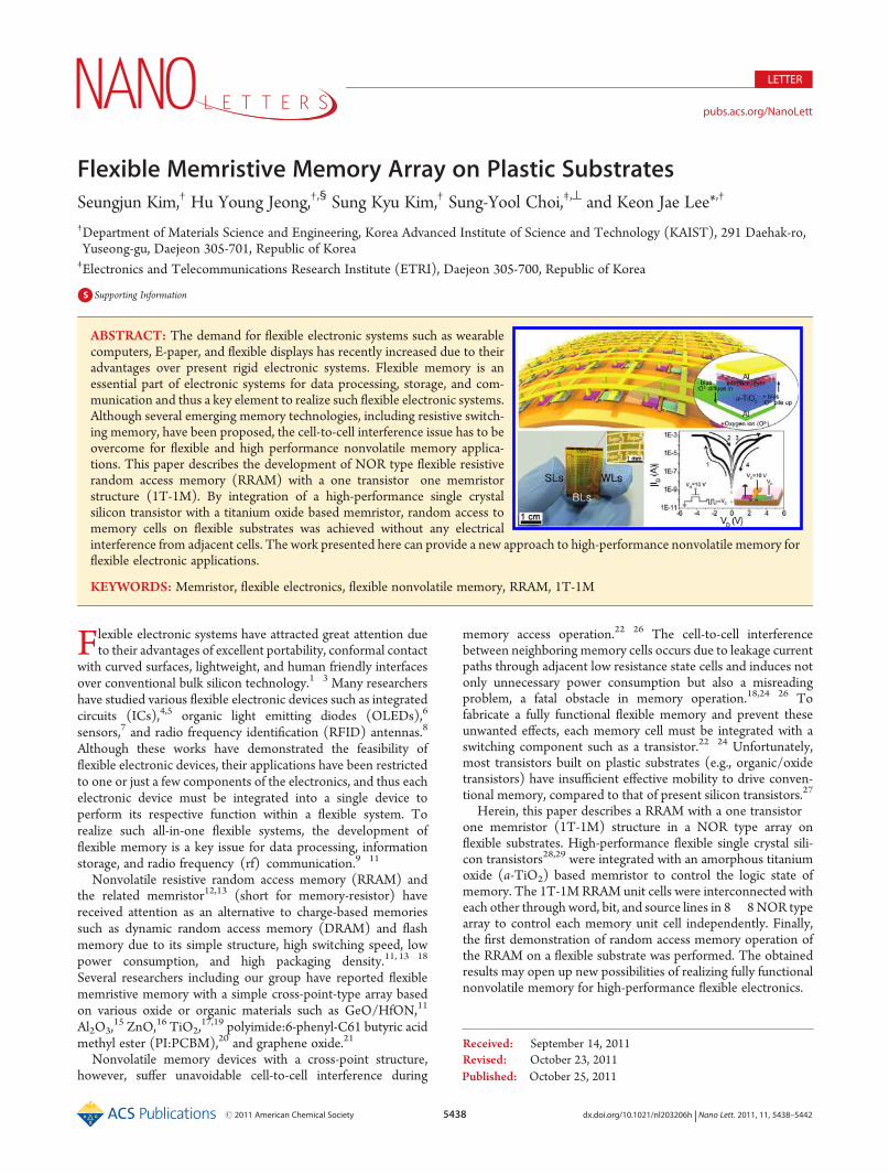
Figure 1a shows a schematic of the device structure for an 8 8flexible RRAM array on a plastic substrate. The n-channel metaloxidesemiconductor field effect transistors (NMOSFET) havechannel length of 10 μm, contact overlap of 20 μm, and channelwidth of 200 μm. Doped silicon nanomembranes (100 nmthickness) on a plastic substrate transferred from a silicon-on-insulator (SOI) wafer were used as an active layer of the transistor,as described in the author’s previous papers.28,29 For a resistanceswitching material, a-TiO2 (14 nm thickness) was depositedbetween the Al top and bottom electrodes by plasma-enhancedatomic layer deposition (PEALD) at the drain region.17 Allmemory cells was interconnected in a NOR type array throughthe word, bit, and source line for random access operation of thememory (see Supporting Information for details on the fabricationof a flexible RRAM on a plastic substrate, Figure S1). Resistanceswitching phenomenon of the a-TiO2 based memristor is believedto be due to the drift of oxygen ions at the top interface layer asvoltage-bias polarity, as depicted in the inset of Figure 1a. The topinterface layer (AlTiO phase) is formed during Al electrodedeposition due to strong oxygen affinity of Al metal. When a
sufficient negative bias is applied to the top electrode, the oxygenions diffuse into the a-TiO2 region, causing the device to switch tothe on state.30,31
Figure 1b shows a magnified optical image of the unit cells ofthe 1T-1M RRAM array corresponding to the circuit diagram inthe inset. The gate and source electrode are respectively con-nected to the word (WL) and source line (SL) in the rowdirection to control the transistor, and the Al top electrode isconnected to the bit line (BL) for logic state change of a memoryunit cell. The integrated transistors play a significant role ofmaintaining the logic state of memory cells when other cells arerandomly accessed, which is the main advantage of this configu-ration over cross-point type circuitry where a switching elementdoes not exist. Figure 1c shows a cross-sectional bright-fieldtransmission electron microscopy (BFTEM) image of uniformmetalinsulatormetal (MIM) layers (120 nm Al/14 nm
Figure 1. (a) A schematic of the device structure for an 8 8 matrixflexible RRAMon a plastic substrate. All memory cells are interconnectedin a NOR type array for random access operation of the memory. Theinset shows schematics of the model for resistive switching of the a-TiO2
based memristor. The arrows in the inset depict the direction of themovement of oxygen ions. (b) A magnified optical image of the unit cellsof RRAM array. The inset shows the structure of a memory unit cell of the1T-1M RRAM and the corresponding circuit diagram. (c) A cross-sectional BFTEM image of an Al/a-TiO2/Al structure on a plasticsubstrate. The upper inset shows the STEM energy dispersive spectros-copy (EDS) elemental mapping of Ti (green), O (blue), and Al (red).The lower inset shows the cross-sectional HRTEM image of the topinterface layer (TIL) and bottom native AlOx layer of Al/a-TiO2/Alstructure. (d) A photograph of the flexible RRAM device and a magnifiedview of unit cells. The metal (Au) pads are connected to WLs, BLs, andSLs for accessing each 1T-1M memory unit cell. The inset shows amagnified view of four memory unit cells and presents the mechanicalstability in a bent state. (e) A photograph of the flexible RRAM devicewrapped on a quartz rod. The inset shows that the flexible RRAM canprovide conformal contact on curvilinear surfaces of two disposable pipets.
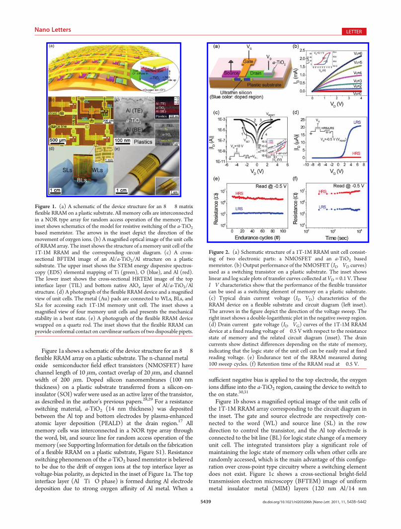
Figure 2. (a) Schematic structure of a 1T-1M RRAM unit cell consist-ing of two electronic parts: a NMOSFET and an a-TiO2 basedmemristor. (b) Output performance of the NMOSFET (IDVD curves)used as a switching transistor on a plastic substrate. The inset showslinear and log scale plots of transfer curves collected at VD = 0.1 V. TheseIV characteristics show that the performance of the flexible transistorcan be used as a switching element of memory on a plastic substrate.(c) Typical drain currentvoltage (IDVD) characteristics of theRRAM device on a flexible substrate and circuit diagram (left inset).The arrows in the figure depict the direction of the voltage sweep. Theright inset shows a double-logarithmic plot in the negative sweep region.(d) Drain currentgate voltage (IDVG) curves of the 1T-1M RRAMdevice at a fixed reading voltage of0.5 V with respect to the resistancestate of memory and the related circuit diagram (inset). The draincurrents show distinct differences depending on the state of memory,indicating that the logic state of the unit cell can be easily read at fixedreading voltage. (e) Endurance test of the RRAM measured during100 sweep cycles. (f) Retention time of the RRAM read at 0.5 V.
5440 dx.doi.org/10.1021/nl203206h |Nano Lett. 2011, 11, 5438–5442
Nano Letters LETTER
a-TiO2/120 nm Al) obtained from ourmemory cell fabricated ona plastic substrate. The elemental mapping of Ti (green), O(blue), and Al (red) by the scanning TEM method in the upperinset clearly indicates the existence of a middle titanium oxidelayer between the two Al metal electrodes. The lower inset is across-sectional high-resolution TEM (HRTEM) image of stackedAl/a-TiO2/Al layers on a plastic substrate, showing the distinctthe top interface layer (TIL)3032 (see Supporting Informationfor TEM analyses of the top interface layer, Figures S2 and S3).Figure 1d presents a photograph of the flexible RRAM device anda magnified view on the plastic substrate. The flexible RRAMconsists of an 8 8 memory cell matrix in a NOR type array withan active area of 1 1 cm2 on a 25 μm thick polyimide film. Themetal (Au) pads are connected toWLs, BLs, and SLs for accessingeach 1T-1M memory unit cell. Figure 1e shows that this devicehas superb mechanical flexibility and does not fracture whenrolled on a quartz rod of 10 mm diameter. Good ductility of themetal line and ultrathin inorganic materials can provide RRAMdevices with good stability on flexible substrates.17,29 The inset ofFigure 1e illustrates that the flexible RRAM can provide con-formal contact on a curvilinear surface. Such flexible capability willbe valuable for implantable and flexible biomedical devices onwrinkled organs such as the brain and intestine.33,34
Figure 2a depicts the schematic structure of a 1T-1M RRAMunit cell consisting of two electronic parts: a NMOSFET and ana-TiO2 based memristor. By applying voltage on the source/drain/gate electrodes, the logic state of the memory elementcan be controlled. Figure 2b shows the output performanceof the NMOSFET (IDVD curves) used as a switching transistoron a plastic substrate. The transistor had effective device mobilityof 340 cm2/(V 3 s) in the linear regime, obtained from the
transfer curve in the inset of Figure 2b with an on/off ratio of105. For resistance switching of the a-TiO2 based memristor,current of at least roughly 300 μA is required to apply requisitevoltage for switching between the top and bottom electrodes.30
This NMOSFET device can easily fulfill this condition at lowoperating voltage (ID ∼ 300 μA at VD = 1 V, VG = 3 V). Theseresults indicate that, in terms of its sufficient current level andon/off ratio, this flexible transistor using ultrathin single crystalsilicon as an active layer can be used as a switching element ofmemory.
Figure 2c shows a typical drain currentvoltage (IDVD)curve of the 1T-1M RRAM device on a flexible substrate, with10 V applied to the gate electrode in order to open the channel.The device is switched from the high-resistance state (HRS) tothe low-resistance state (LRS) by sweeping the drain voltagefrom 0 V to a negative value over the SET voltage (VSET). TheLRS is retained during the voltage sweep back to a positiveRESET voltage (VRESET) and converts to the HRS at a highervoltage than VRESET. This indicates that our RRAM device hasasymmetric bipolar resistance switching (BRS) behavior with anon/off ratio of 50 at 0.5 V (reading voltage).
In order to investigate the current conduction mechanism indetail, double-logarithmic plots of the IDVD curve for thenegative voltage regions are illustrated in the right inset ofFigure 2c. The log IDVD plot of HRS shows Ohmic conductionbehavior (|ID| |VD|) in the low voltage region (<0.2 V) andgradually changed to a square dependence (|ID| |VD|
2), asdepicted in the inset of Figure 3c. This behavior is qualitativelyinterpreted to follow the shallow trap-associated space-charge-limited conduction (SCLC) theory, which is generally expressedby I(V) = aV + bV2.35,36 It is interesting that the slope of the logIlog V plot in the high-voltage region of the LRS is slightlylower than two (1.7). This BRS behavior of Al/a-TiO2/Almemory devices can be explained by the change of trap distribu-tions in the top interface layer (AlTiO), which originatesfrom the motion of oxygen ions due to external bias.30,32
Figure 2d presents drain currentgate voltage (IDVG) curvesof the RRAM device at a fixed reading voltage of 0.5 V in theLRS and HRS. The drain currents show distinct differencesdepending on the state of memory, indicating that the logic stateof the unit cell can be easily read at fixed reading voltage.23
Endurance and retention tests were conducted in order toinvestigate the reliability of the flexible RRAM. Figure 2e showsthe endurance cycling test results at a reading voltage of 0.5 Vobtained by repetitive on/off sweeping operation. During 100endurance cycles, both the HRS and LRS retain their resistancevalues without significant change at the reading voltage, showingreproducible resistive switching. The retention property ofRRAM was also characterized at room temperature to evaluatethe data storage ability, and the results are shown in Figure 2f.The RRAM on the flexible substrate shows good retentioncharacteristics up to 104 s without electrical degradation in boththe LRS and HRS.
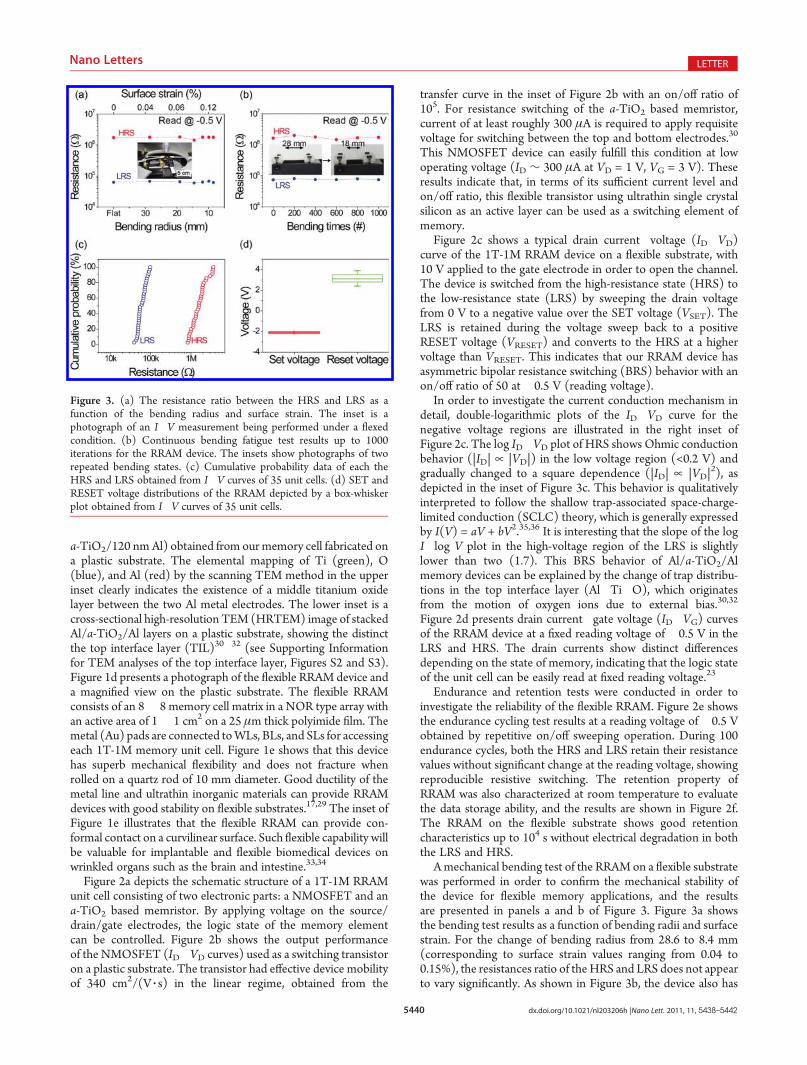
Amechanical bending test of the RRAMon a flexible substratewas performed in order to confirm the mechanical stability ofthe device for flexible memory applications, and the resultsare presented in panels a and b of Figure 3. Figure 3a showsthe bending test results as a function of bending radii and surfacestrain. For the change of bending radius from 28.6 to 8.4 mm(corresponding to surface strain values ranging from 0.04 to0.15%), the resistances ratio of theHRS and LRS does not appearto vary significantly. As shown in Figure 3b, the device also has
Figure 3. (a) The resistance ratio between the HRS and LRS as afunction of the bending radius and surface strain. The inset is aphotograph of an IV measurement being performed under a flexedcondition. (b) Continuous bending fatigue test results up to 1000iterations for the RRAM device. The insets show photographs of tworepeated bending states. (c) Cumulative probability data of each theHRS and LRS obtained from IV curves of 35 unit cells. (d) SET andRESET voltage distributions of the RRAM depicted by a box-whiskerplot obtained from IV curves of 35 unit cells.

5441 dx.doi.org/10.1021/nl203206h |Nano Lett. 2011, 11, 5438–5442
Nano Letters LETTER
good mechanical endurance during a bending fatigue test invol-ving 1000 iterations of bending. A statistical analysis was con-ducted for the flexible RRAM to examine the uniformity of thedevice, and the results are given in panels c and d of Figure 3. Thefinal yield of our integrated device that shows the stable 1T-1Mworking condition was about 60%. However, we believe thatdevice yield would be improved if we adopt an automatedfabrication process37 or simple device structure such as onediodeone unipolar resistor (1D-1R) RRAM.22 Figure 3c showsthe cumulative probability data for each resistance state. Both theHRS and LRS exhibit a narrow distribution with good separa-tion between the HRS and LRS. Figure 3d shows the SET andRESET voltage distributions obtained from IV curves. Thedistribution of the RESET voltage is slightly broader than thatof the SET voltage. It seems that the contact resistance variation,caused by the nonuniform spin-on-doping (SOD) technique,more deeply influences output characteristics in positive voltageregion.38
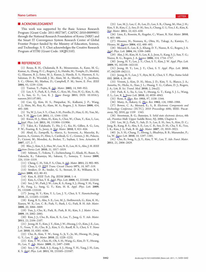
Figure 4a shows a schematic illustration of the random accessoperation for our 2 2 flexible RRAM cells in 8 8 memoryarrays, and their operation conditions are summarized inFigure 4b. Fundamentally, the prevention of cell-to-cell inter-ference during memory access operation can be confirmed bymeasuring 2 2 cells22,24 and these results can be applied to the
multi n nmemory cells operations.22,24,25,39 The initial state ofall memory cells was set to the HRS. By applying the SET pulseon the word and bit lines, (1, 1), (1, 2), and (2, 1) cells aresequentially converted from the HRS to the LRS (the writingprocess, see Figure S7i-iii in the Supporting Information). Afterthe writing process of the above three cells is completed, theREAD pulse (10 V to WL2, 0.5 V to BL2, and 4 V to WL1)was applied to the (2, 2) cell in order to read the memory cellstate. The correct HRS signal (1.96 MΩ) of the selected (2, 2)cell can be read without any influence or interference from othermemory cells. However, for the case of a cross-point structurewhere the switching component does not exist, an independentread operation is not possible due to the electrical leakage path,called a sneak path, as illustrated in Figure 4c.2226 On thecontrary, our 1T-1M RRAM removes the sneak path by turningoff unaddressed memory cells and enables random accessoperation, as depicted in Figure 4d. Finally, after the (2, 2) cellwas converted to the LRS by applying the SET pulse, all memorycells were returned back to the HRS in the order of (2, 2), (2, 1),(1, 2), (1, 1) by applying the RESET pulse to demonstrate theerasing process (see Figures S48, Supporting Information, fordetails of the writing/reading/erasing process).
In summary, we demonstrate a flexible 1T-1M RRAM arraythat is driven by high-performance flexible transistors and mem-ristors. For fully functional and independent memory operationsof writereaderase, all memory cells were integrated with eachother in a NOR type array. The developed device exhibitedreliable and reproducible resistive switching, endurance, andretention properties. The flexible RRAM also had excellentmechanical stability upon harsh bending. The NOR typeRRAM showed successful random access operation withoutany electrical interference. This flexible RRAM is expected toprovide opportunities for neuromorphic devices40 and otherflexible memory structures such as 1D-1R memory22 and three-dimensional (3D) stacking memory41 for high device yield andpacking density.
’ASSOCIATED CONTENT
bS Supporting Information. The detailed fabrication proce-dures of flexible 1T-1M NOR type RRAM on a plastic substrate(Figure S1), ADF-STEM and BF-STEM images of Al/a-TiO2/Almemristor (Figure S2), magnified ADF-STEM image and corre-sponding EDS line elemental profile taken from the top Alelectrode to bottom (Figure S3), selection of the transistor turn-off voltage (Figure S4), resistance behavior in transistor OFFcondition (Figure S5), and random access operation for 2 2flexible RRAM cells (Figures S68). This material is availablefree of charge via the Internet at http://pubs.acs.org.
’AUTHOR INFORMATION
Corresponding Author*E-mail: [email protected].
Present Addresses§School ofMechanical & AdvancedMaterials Engineering, UlsanNational Institute of Science and Technology (UNIST), Ulsan689-798, Republic of Korea.^Department of Electrical Engineering, Korea Advanced Insti-tute of Science and Technology (KAIST), 291 Daehak-ro,Yuseong-gu, Daejeon 305-701, Republic of Korea.
Figure 4. (a) Schematic illustration of the random access operation of2 2 flexible RRAM cells. After the write process of (1, 1), (1, 2), and(2, 1) cells, the correct HRS signal (1.96 MΩ) of the selected (2, 2) cellcan be read by applying the READpulse onword and bit lines without anyinfluence or interference from other memory cells. (b) Operationconditions for the memory cells arranged in a NOR type array. All pulsewidths for SET/RESET/READ are fixed at 50 ms. (c) Illustration of across-point memory structure. The red and green lines indicate selectedand unselected lines, respectively. The white dotted line denotes apossible misreading path (sneak path) through three neighboring lowresistance cells. (d) An illustration of a 1T-1M RRAM structure.The red and green lines denote selected and unselected lines, respectively.The 1T-1M RRAM removes the electrical leakage path by turning offunaddressed memory cells and enables random access operation. Thewhite arrows denote a correct data flow corresponding to the state of the(2, 2) cell.
5442 dx.doi.org/10.1021/nl203206h |Nano Lett. 2011, 11, 5438–5442
Nano Letters LETTER
’ACKNOWLEDGMENT
This work was supported by the Basic Science ResearchProgram (Grant Code: 2011-0027367, CAFDC-2010-0009903)through the National Research Foundation of Korea (NRF) andthe Smart IT Convergence System Research Center of GlobalFrontier Project funded by the Ministry of Education, Science,and Technology. S. Y. Choi acknowledges the Creative ResearchProgram of ETRI (Grant Code: 10QB1310).
’REFERENCES
(1) Reuss, R. H.; Chalamala, B. R.; Moussessian, A.; Kane, M. G.;Kumar, A.; Zhang, D. C.; Rogers, J. A.; Hatalis, M.; Temple, D.; Moddel,G.; Eliasson, B. J.; Estes, M. J.; Kunze, J.; Handy, E. S.; Harmon, E. S.;Salzman, D. B.; Woodall, J. M.; Alam, M. A.; Murthy, J. Y.; Jacobsen,S. C.; Olivier, M.; Markus, D.; Campbell, P. M.; Snow, E. Proc. IEEE2005, 93, 1239–1256.(2) Tsutsui, T.; Fujita, K. Adv. Mater. 2002, 14, 949–952.(3) Lee, S. Y.; Park, K. I.; Huh, C.; Koo, M.; Yoo, H. G.; Kim, S.; Ah,
C. S.; Sun, G. Y.; Lee, K. J. Nano Energy 2011, DOI: 10.1016/j.nanoen.2011.07.001.(4) Cao, Q.; Kim, H. S.; Pimparkar, N.; Kulkarni, J. P.; Wang,
C. J.; Shim, M.; Roy, K.; Alam, M. A.; Rogers, J. A. Nature 2008, 454,495–500.(5) Yu,W. J.; Lee, S. Y.; Chae, S. H.; Perello, D.; Han, G. H.; Yun,M.;
Lee, Y. H. Nano Lett. 2011, 11, 1344–1350.(6) Kwon, H. J.; Shim, H.; Kim, S.; Choi, W.; Chun, Y.; Kee, I.; Lee,
S. Appl. Phys. Lett. 2011, 98, 151904–151906.(7) Takei, K.; Takahashi, T.; Ho, J. C.; Ko, H.; Gillies, A. G.; Leu,
P. W.; Fearing, R. S.; Javey, A. Nat. Mater. 2010, 9, 821–826.(8) Abad, E.; Zampolli, S.; Marco, S.; Scorzoni, A.; Mazzolai, B.;
Juarros, A.; Gomez, D.; Elmi, I.; Cardinali, G. C.; Gomez, J. M.; Palacio,F.; Cicioni, M.; Mondini, A.; Becker, T.; Sayhan, I. Sens. Actuators, B2007, 127, 2–7.(9) Rho, J.; Kim, S. J.; Heo,W.; Lee, N. E.; Lee, H. S.; Ahn, J. H. IEEE
Electron Device Lett. 2010, 31, 1017–1019.(10) Sekitani, T.; Yokota, T.; Zschieschang, U.; Klauk, H.; Bauer, S.;
Takeuchi, K.; Takamiya, M.; Sakurai, T.; Someya, T. Science 2009,326, 1516–1519.(11) Cheng, C. H.; Yeh, F. S.; Chin, A. Adv. Mater. 2011, 23, 902–905.(12) Chua, L. O. IEEE Trans. Circuit Theory 1971, 18, 507–519.(13) Strukov, D. B.; Snider, G. S.; Stewart, D. R.; Williams, R. S.
Nature 2008, 453, 80–83.(14) Kim, K. IEEE Tech. Dig. IEDM 2010, 1–4.(15) Kim, S.; Choi, Y. K. Appl. Phys. Lett. 2008, 92, 223508–223510.(16) Seo, J. W.; Park, J. W.; Lim, K. S.; Kang, S. J.; Hong, Y. H.; Yang,
J. H.; Fang, L.; Sung, G. Y.; Kim, H. K. Appl. Phys. Lett. 2009,95, 133508–133510.(17) Jeong, H. Y.; Kim, Y. I.; Lee, J. Y.; Choi, S. Y. Nanotechnology
2010, 21, 115203–115208.(18) Kang, B. S.; Ahn, S. E.; Lee, M. J.; Steftinovich, G.; Kim, K. H.;
Xianyu, W. X.; Lee, C. B.; Park, Y.; Baek, I. G.; Park, B. H. Adv. Mater.2008, 20, 3066–3069.(19) Yun, J.; Cho, K.; Park, B.; Park, B. H.; Kim, S. J. Mater. Chem.
2009, 19, 2082–2085.(20) Kim, J. J.; Cho, B.; Kim, K. S.; Lee, T.; Jung, G. Y. Adv. Mater.
2011, 23, 2104–2107.(21) Jeong, H. Y.; Kim, J. Y.; Kim, J. W.; Hwang, J. O.; Kim, J. E.; Lee,
J. Y.; Yoon, T. H.; Cho, B. J.; Kim, S. O.; Ruoff, R. S.; Choi, S. Y. NanoLett. 2010, 10, 4381–4386.(22) Cho, B.; Kim, T. W.; Song, S.; Ji, Y.; Jo, M.; Hwang, H.; Jung,
G. Y.; Lee, T. Adv. Mater. 2010, 22, 1228–1232.(23) Kim, T. W.; Choi, H.; Oh, S. H.; Wang, G.; Kim, D. Y.; Hwang,
H.; Lee, T. Adv. Mater. 2009, 21, 2497–2500.(24) Seo, J. W.; Baik, S. J.; Kang, S. J.; Hong, Y. H.; Yang, J. H.; Lim,
K. S. Appl. Phys. Lett. 2011, 98, 233505–233507.
(25) Lee, M. J.; Lee, C. B.; Lee, D.; Lee, S. R.; Chang, M.; Hur, J. H.;Kim, Y. B.; Kim, C. J.; Seo, D. H.; Seo, S.; Chung, U. I.; Yoo, I. K.; Kim, K.Nat. Mater. 2011, 10, 625–630.
(26) Linn, E.; Rosezin, R.; Kugeler, C.; Waser, R. Nat. Mater. 2010,9, 403–406.
(27) Hosono, H.; Nomura, K.; Ohta, H.; Takagi, A.; Kamiya, T.;Hirano, M. Nature 2004, 432, 488–492.
(28) Menard, E.; Lee, K. J.; Khang, D. Y.; Nuzzo, R. G.; Rogers, J. A.Appl. Phys. Lett. 2004, 84, 5398–5400.
(29) Ahn, J. H.; Kim, H. S.; Lee, K. J.; Jeon, S.; Kang, S. J.; Sun, Y. G.;Nuzzo, R. G.; Rogers, J. A. Science 2006, 314, 1754–1757.
(30) Jeong, H. Y.; Lee, J. Y.; Choi, S. Y.; Kim, J. W. Appl. Phys. Lett.2009, 95, 162108–162110.
(31) Jeong, H. Y.; Lee, J. Y.; Choi, S. Y. Appl. Phys. Lett. 2010,97, 042109–042111.
(32) Jeong, H. Y.; Lee, J. Y.; Ryu, M. K.; Choi, S. Y. Phys. Status SolidiRRL 2010, 4, 28–30.
(33) Viventi, J.; Kim, D. H.; Moss, J. D.; Kim, Y. S.; Blanco, J. A.;Annetta, N.; Hicks, A.; Xiao, J. L.; Huang, Y. G.; Callans, D. J.; Rogers,J. A.; Litt, B. Sci. Transl. Med. 2010, 2, 24ra22.
(34) Park, K. I.; Xu, S.; Liu, Y.; Hwang, G. T.; Kang, S. J. L.; Wang,Z. L.; Lee, K. J. Nano Lett. 2010, 10, 4939–4943.
(35) Rose, A. Phys. Rev. 1955, 97, 1538–1544.(36) Many, A.; Rakavy, G. Phys. Rev. 1962, 126, 1980–1988.(37) Bower, C. A.; Menard, E.; S., B. Electronic Components and
Technology Conference (ECTC), 2010 Proceedings 60th; IEEE: Piscat-away, NJ, 2010, pp 13391343.
(38) Streetman, B. G.; Banerjee, S. Solid state electronic devices, 6thed.; Prentice Hall: Upper Saddle River, NJ, 2006; Chapter 6.
(39) Lee, M. J.; Park, Y.; Suh, D. S.; Lee, E. H.; Seo, S.; Kim, D. C.;Jung, R.; Kang, B. S.; Ahn, S. E.; Lee, C. B.; Seo, D. H.; Cha, Y. K.; Yoo,I. K.; Kim, J. S.; Park, B. H. Adv. Mater. 2007, 19, 3919–3923.
(40) Jo, S. H.; Chang, T.; Ebong, I.; Bhadviya, B. B.; Mazumder, P.;Lu, W. Nano Lett. 2010, 10, 1297–1301.
(41) Cho, B.; Song, S.; Ji, Y.; Kim, T. W.; Lee, T. Adv. Funct. Mater.2011, 21, 2806–2829.
1
Supporting Information for:
Flexible Memristive Memory Array on Plastic Substrates
Seungjun Kim1, Hu Young Jeong1#, Sung Kyu Kim1, Sung-Yool Choi2 and Keon Jae Lee1*
1Department of Materials Science and Engineering, Korea Advanced Institute of Science and
Technology (KAIST), 291 Daehak-ro, Yuseong-gu, Daejeon 305-701 Republic of Korea 2Electronics and Telecommunications Research Institute (ETRI), Daejeon 305-700 Republic of
Korea #present address: School of Mechanical & Advanced Materials Engineering, Ulsan National
Institute of Science and Technology (UNIST), Ulsan 689-798 Republic of Korea
*e-mail: [email protected], (Phone) 82-42-350-3343, (Fax) 82-42-350-3310
2
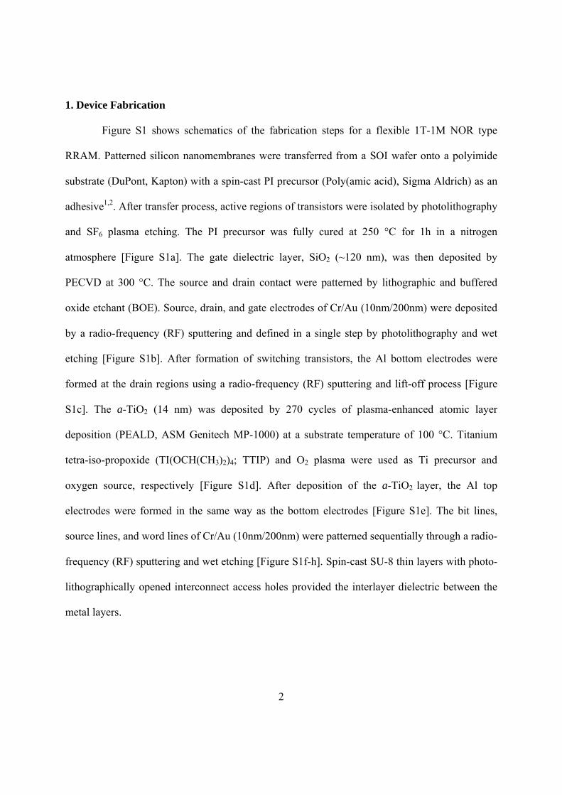
1. Device Fabrication
Figure S1 shows schematics of the fabrication steps for a flexible 1T-1M NOR type
RRAM. Patterned silicon nanomembranes were transferred from a SOI wafer onto a polyimide
substrate (DuPont, Kapton) with a spin-cast PI precursor (Poly(amic acid), Sigma Aldrich) as an
adhesive1,2. After transfer process, active regions of transistors were isolated by photolithography
and SF6 plasma etching. The PI precursor was fully cured at 250 °C for 1h in a nitrogen
atmosphere [Figure S1a]. The gate dielectric layer, SiO2 (~120 nm), was then deposited by
PECVD at 300 °C. The source and drain contact were patterned by lithographic and buffered
oxide etchant (BOE). Source, drain, and gate electrodes of Cr/Au (10nm/200nm) were deposited
by a radio-frequency (RF) sputtering and defined in a single step by photolithography and wet
etching [Figure S1b]. After formation of switching transistors, the Al bottom electrodes were
formed at the drain regions using a radio-frequency (RF) sputtering and lift-off process [Figure
S1c]. The a-TiO2 (14 nm) was deposited by 270 cycles of plasma-enhanced atomic layer
deposition (PEALD, ASM Genitech MP-1000) at a substrate temperature of 100 °C. Titanium
tetra-iso-propoxide (TI(OCH(CH3)2)4; TTIP) and O2 plasma were used as Ti precursor and
oxygen source, respectively [Figure S1d]. After deposition of the a-TiO2 layer, the Al top
electrodes were formed in the same way as the bottom electrodes [Figure S1e]. The bit lines,
source lines, and word lines of Cr/Au (10nm/200nm) were patterned sequentially through a radio-
frequency (RF) sputtering and wet etching [Figure S1f-h]. Spin-cast SU-8 thin layers with photo-
lithographically opened interconnect access holes provided the interlayer dielectric between the
metal layers.
3
Figure S1.
4
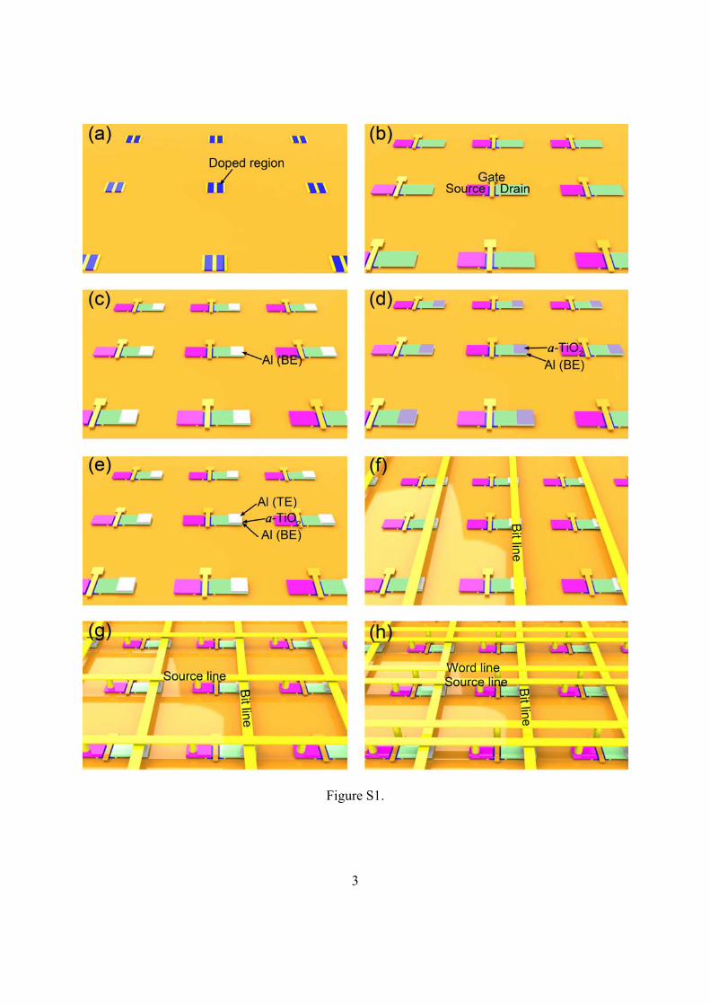
2. TEM analyses
A. ADF and BF image
The annular dark field (ADF) STEM image and BF STEM image were taken by using an
aberration-corrected STEM (JEM -2100F) operated at accelerating voltage 200kV. As shown in
Figure S2, a titanium oxide thin film could be clearly separated between two Al electrodes due to
atomic z-contrast. From low magnification images, it can be seen that the titanium oxide thin film
is uniformly deposited even on rough Al bottom electrode surface by atomic layer deposition
process.
Figure S2.
5
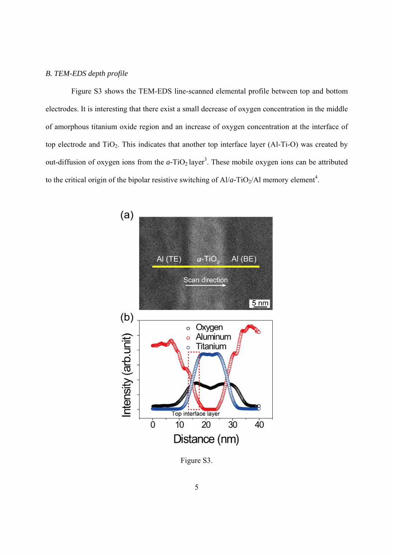
B. TEM-EDS depth profile
Figure S3 shows the TEM-EDS line-scanned elemental profile between top and bottom
electrodes. It is interesting that there exist a small decrease of oxygen concentration in the middle
of amorphous titanium oxide region and an increase of oxygen concentration at the interface of
top electrode and TiO2. This indicates that another top interface layer (Al-Ti-O) was created by
out-diffusion of oxygen ions from the a-TiO2 layer3. These mobile oxygen ions can be attributed
to the critical origin of the bipolar resistive switching of Al/a-TiO2/Al memory element4.
Figure S3.

6
3. Selection of the transistor turn-off voltage
To prevent the cross-talk interference, switching transistor components are necessary. A
switching transistor should have sufficient output performance to drive memory in the ON state
as well as enough resistance to remove leakage current paths in OFF state. Figure S4a-b depicts a
schematic of switching Si MOS transistor on a flexible substrate and its corresponding ID-VD
curves in negative gate/drain voltage region. From these ID-VD curves, the gate voltage of -4 V
was selected for turning off a transistor.
Figure S4.

7
4. Resistance behaviour in transistor OFF condition
Figure S5a shows a 1T-1M flexible memory cell where the negative voltage sweep (0 V
→ -4.5 V→ 0 V) is applied on the HRS memory element during transistor off condition and its
corresponding ID-VD characteristics presents in Figure S5b. In contrast to memory cells with
transistor on condition (VG= 10 V) in Figure 2c, the resistance switching of HRS memory state
was not observed during voltage sweep. Similarly, there is no resistance switching in a LRS
memory cell during positive voltage sweep (0 V → 4.5 V→ 0 V) as shown in Figure S5c-d.
Figure S5e presents that resistance changes, measured at a reading voltage condition of -0.5 V
with 10 V of VG, did not occur during negative/positive voltage sweeps.

8
Figure S5.
9
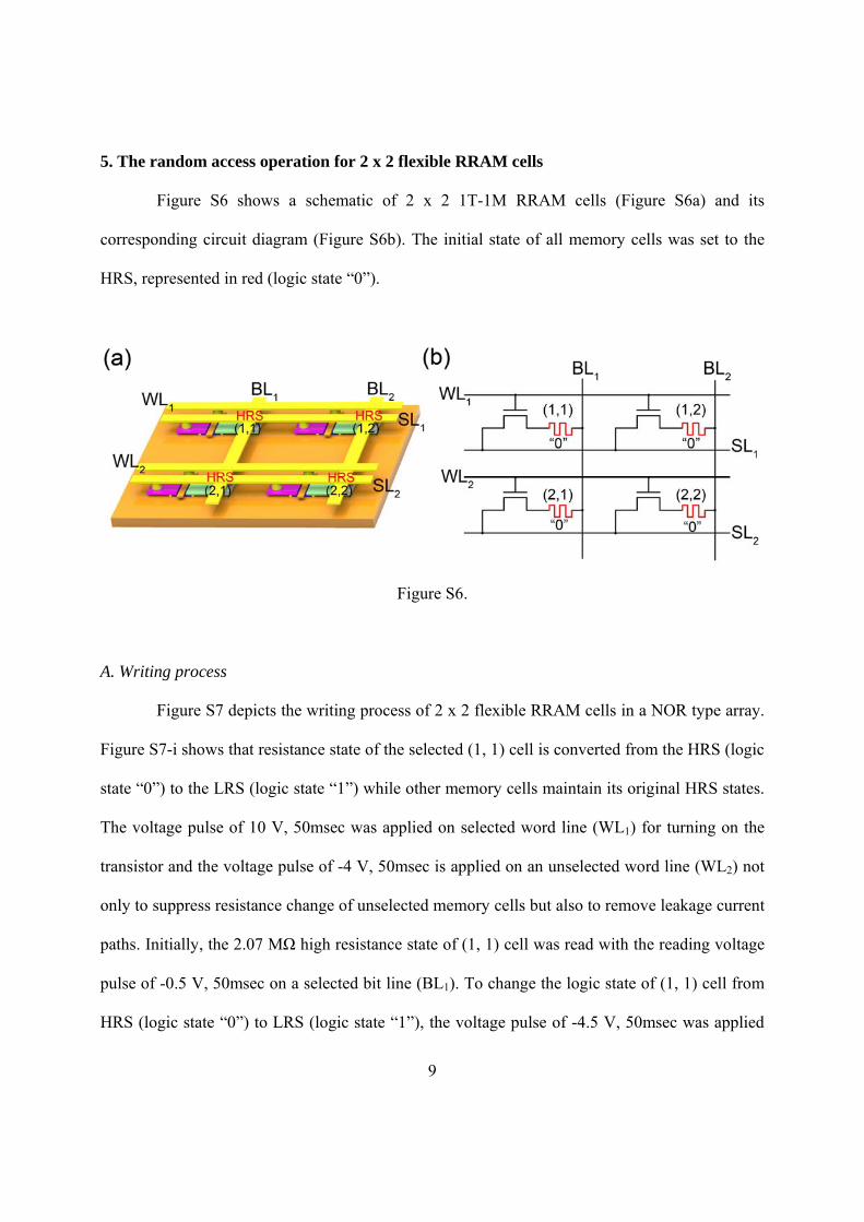
5. The random access operation for 2 x 2 flexible RRAM cells
Figure S6 shows a schematic of 2 x 2 1T-1M RRAM cells (Figure S6a) and its
corresponding circuit diagram (Figure S6b). The initial state of all memory cells was set to the
HRS, represented in red (logic state “0”).
Figure S6.
A. Writing process
Figure S7 depicts the writing process of 2 x 2 flexible RRAM cells in a NOR type array.
Figure S7-i shows that resistance state of the selected (1, 1) cell is converted from the HRS (logic
state “0”) to the LRS (logic state “1”) while other memory cells maintain its original HRS states.
The voltage pulse of 10 V, 50msec was applied on selected word line (WL1) for turning on the
transistor and the voltage pulse of -4 V, 50msec is applied on an unselected word line (WL2) not
only to suppress resistance change of unselected memory cells but also to remove leakage current
paths. Initially, the 2.07 MΩ high resistance state of (1, 1) cell was read with the reading voltage
pulse of -0.5 V, 50msec on a selected bit line (BL1). To change the logic state of (1, 1) cell from
HRS (logic state “0”) to LRS (logic state “1”), the voltage pulse of -4.5 V, 50msec was applied

10
on a selected bit line. After switching logic state, the 86.8 kΩ low resistance state of (1, 1) cell
was read with same reading voltage pulse. Similarly, logic states of other memory cells were
sequentially converted from HRS “0” to LRS “1” in the order of (1, 2), (2, 1), (2, 2) through the
writing process described in the above.
Figure S7.

11
B. Erasing process
Figure S8 shows the erasing process of 2 x 2 flexible RRAM cells in a NOR type array.
Figure S8-i shows that resistance state of the selected (2, 2) cell is converted from the LRS (logic
state “1”) to the HRS (logic state “0”) while other memory cells maintain its LRS states. To
change the logic state of (2, 2) cell from LRS (logic state “1”) to HRS (logic state “0”), the
voltage pulse of 5.5 V, 50msec was applied on a selected bit line with the voltage pulse of 10 V,
50msec to WL2 and -4 V, 50msec to WL1. After switching logic state, the 1.60 MΩ high
resistance state of (2, 2) cell was read with same reading voltage pulse. Similarly, logic states of
other memory cells were sequentially converted from LRS “1” to HRS “0” in the order of (2, 1),
(1, 2), (1, 1) through the erasing process described in the above.
Figure S8.

12
REFERENCES
1. Lee, K.J. et al. Large-area, selective transfer of microstructured silicon: A printing-based
approach to high-performance thin-film transistors supported on flexible substrates. Adv.
Mater. 17, 2332-2336 (2005).
2. Ahn, J.H. et al. Heterogeneous three-dimensional electronics by use of printed
semiconductor nanomaterials. Science 314, 1754-1757 (2006).
3. Jeong, H.Y., Lee, J.Y., Choi, S.Y. & Kim, J.W. Microscopic origin of bipolar resistive
switching of nanoscale titanium oxide thin films. Appl. Phys. Lett. 95, 162108-162110
(2009).
4. Jeong, H.Y., Lee, J.Y., Ryu, M.K. & Choi, S.Y. Bipolar resistive switching in amorphous
titanium oxide thin film. Phys. Status Solidi RRL 4, 28-30 (2010).
13
FIGURE CAPTIONS
Figure S1. Schematic illustration of the process for fabricating of flexible 1T-1M NOR type
RRAM on a plastic substrate. (a) transfer-printing of silicon nanomembrane onto polyimide
substrate. (b) Fabrication of switching transistors. (c) Deposition of Al bottom electrodes. (d)
Deposition of a-TiO2 using PEALD. (e) Deposition of Al top electrodes. (f)-(h) Interconnection
of memory cells through word, source, and bit lines.
Figure S2. (a) ADF-STEM and (b) BF-STEM images of our Al/a-TiO2/Al memristor on plastic
substrate.
Figure S3. (a) Magnified ADF-STEM image and corresponding (b) EDS line elemental profile
taken from the top Al electrode to bottom.
Figure S4. (a) Schematic structure of switching transistor (b) ID-VD curves of the switching
transistor in negative gate/drain voltage region.
Figure S5. (a) Schematic structure of a RRAM unit cell in the HRS state. (b) ID-VD
characteristics of a RRAM unit cell in the HRS state during negative voltage sweep (0 V → -4.5
V→ 0 V). (c) Schematic structure of a RRAM unit cell in the LRS state. (d) ID-VD characteristics
of a RRAM unit cell in the LRS state during positive voltage sweep (0 V → 4.5 V→ 0 V). (e)
Before and after resistance value. Any significant resistance changes do not occur.
Figure S6. (a) Schematic of 2 x 2 RRAM cells in a NOR type array. (b) Circuit diagram
corresponding to Figure S6a. Red colour denotes the HRS (logic state “0”).
Figure S7. The writing process of 2 x 2 flexible RRAM cells in a NOR type array. Red color
denotes the HRS (logic state “0”) and blue colour denotes the LRS (logic state “1”).
Figure S8. The erasing process of 2 x 2 flexible RRAM cells in a NOR type array. Red color
denotes the HRS (logic state “0”) and blue colour denotes the LRS (logic state “1”).