Field Programmable Gate Arrays 14... · 2018-02-05 · PROM PLA a b c & & & a !a b !b c !c N/A...
116
Field Programmable Gate Arrays TIE-50206 Logic Synthesis Arto Perttula Tampere University of Technology Spring 2018
Transcript of Field Programmable Gate Arrays 14... · 2018-02-05 · PROM PLA a b c & & & a !a b !b c !c N/A...
Field Programmable Gate
Arrays
TIE-50206 Logic Synthesis
Arto Perttula
Tampere University of Technology
Spring 2018
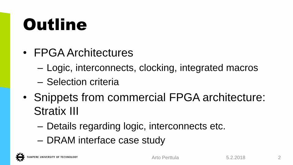
Outline
• FPGA Architectures
– Logic, interconnects, clocking, integrated macros
– Selection criteria
• Snippets from commercial FPGA architecture:
Stratix III
– Details regarding logic, interconnects etc.
– DRAM interface case study
5.2.2018Arto Perttula 2
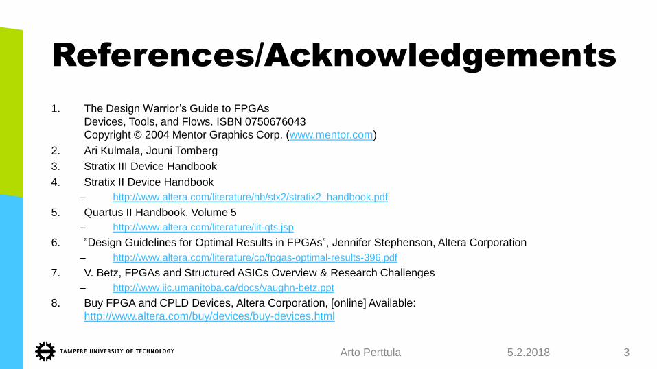
References/Acknowledgements
1. The Design Warrior’s Guide to FPGAs
Devices, Tools, and Flows. ISBN 0750676043
Copyright © 2004 Mentor Graphics Corp. (www.mentor.com)
2. Ari Kulmala, Jouni Tomberg
3. Stratix III Device Handbook
4. Stratix II Device Handbook
– http://www.altera.com/literature/hb/stx2/stratix2_handbook.pdf
5. Quartus II Handbook, Volume 5
– http://www.altera.com/literature/lit-qts.jsp
6. ”Design Guidelines for Optimal Results in FPGAs”, Jennifer Stephenson, Altera Corporation
– http://www.altera.com/literature/cp/fpgas-optimal-results-396.pdf
7. V. Betz, FPGAs and Structured ASICs Overview & Research Challenges
– http://www.iic.umanitoba.ca/docs/vaughn-betz.ppt
8. Buy FPGA and CPLD Devices, Altera Corporation, [online] Available:
http://www.altera.com/buy/devices/buy-devices.html
5.2.2018Arto Perttula 3
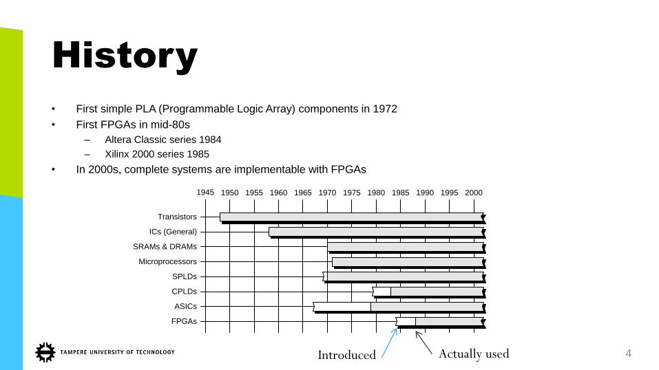
History
• First simple PLA (Programmable Logic Array) components in 1972
• First FPGAs in mid-80s
– Altera Classic series 1984
– Xilinx 2000 series 1985
• In 2000s, complete systems are implementable with FPGAs
4
1945 1950 1955 1960 1965 1970 1975 1980 1985 1990 1995 2000
FPGAs
ASICs
CPLDs
SPLDs
Microprocessors
SRAMs & DRAMs
ICs (General)
Transistors
Introduced Actually used
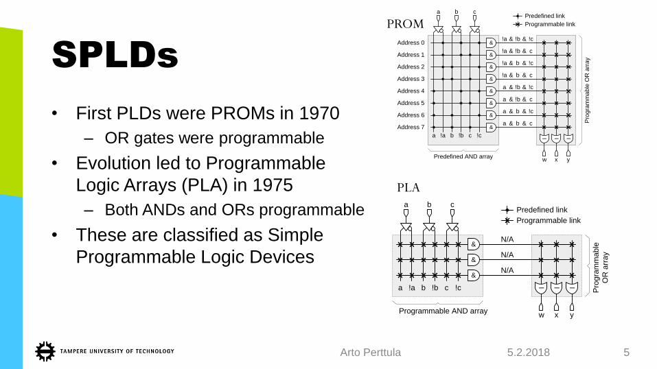
SPLDs
• First PLDs were PROMs in 1970
– OR gates were programmable
• Evolution led to Programmable
Logic Arrays (PLA) in 1975
– Both ANDs and ORs programmable
• These are classified as Simple
Programmable Logic Devices
5.2.2018Arto Perttula 5
a b c
l l l
Address 0 &
Address 1 &
Address 2 &
Address 3 &
Address 4 &
Address 5 &
Address 6 &
Address 7 &
a !a b !b c !c
!a !c!b& &
!a c!b& &
!a !cb& &
!a cb& &
a !c!b& &
a c!b& &
a !cb& &
a cb& &
Predefined AND array
Pro
gra
mm
ab
le O
R a
rra
y
w x y
Predefined link
Programmable linkPROM
PLAa b c
&
&
&
a !a b !b c !c
N/A
Programmable AND array
Pro
gra
mm
ab
le
OR
arr
ay
Predefined link
Programmable link
l l l
w x y
N/A
N/A
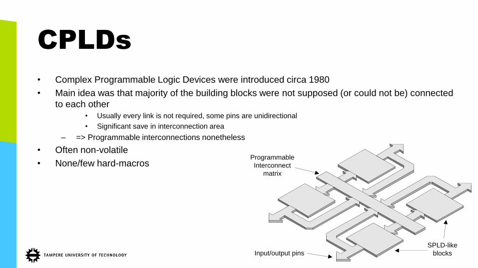
CPLDs
• Complex Programmable Logic Devices were introduced circa 1980
• Main idea was that majority of the building blocks were not supposed (or could not be) connected
to each other
• Usually every link is not required, some pins are unidirectional
• Significant save in interconnection area
– => Programmable interconnections nonetheless
• Often non-volatile
• None/few hard-macrosProgrammable
Interconnect
matrix
Input/output pins
SPLD-like
blocks
FPGAs
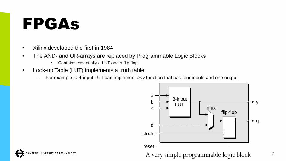
• Xilinx developed the first in 1984
• The AND- and OR-arrays are replaced by Programmable Logic Blocks
• Contains essentially a LUT and a flip-flop
• Look-up Table (LUT) implements a truth table
– For example, a 4-input LUT can implement any function that has four inputs and one output
7A very simple programmable logic block
3-inputLUT
a
b
cflip-flop
clock
mux
y
qd
reset
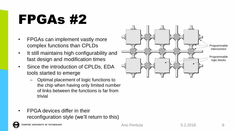
FPGAs #2
• FPGAs can implement vastly more
complex functions than CPLDs
• It still maintains high configurability and
fast design and modification times
• Since the introduction of CPLDs, EDA
tools started to emerge
– Optimal placement of logic functions to
the chip when having only limited number
of links between the functions is far from
trivial
• FPGA devices differ in their
reconfiguration style (we’ll return to this)
5.2.2018Arto Perttula 8
Programmable
interconnect
Programmable
logic blocks

FPGA ARCHITECTURES
5.2.2018Arto Perttula 9
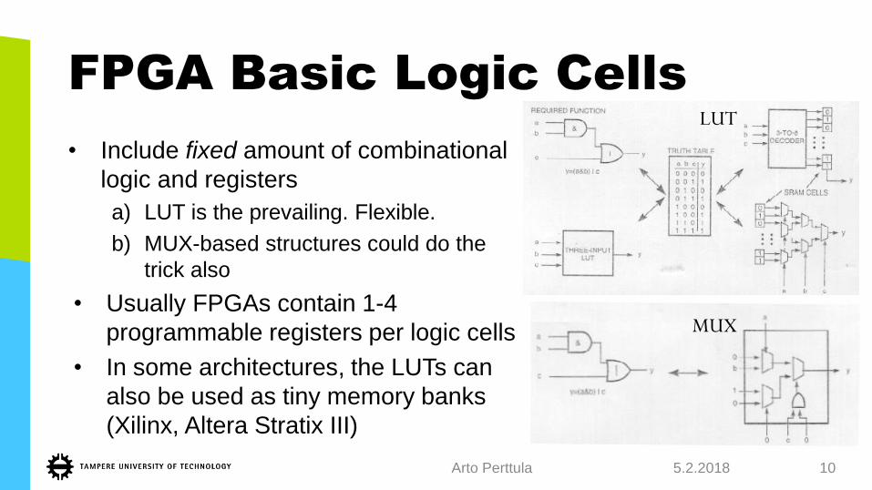
FPGA Basic Logic Cells
• Include fixed amount of combinational
logic and registers
a) LUT is the prevailing. Flexible.
b) MUX-based structures could do the
trick also
• Usually FPGAs contain 1-4
programmable registers per logic cells
• In some architectures, the LUTs can
also be used as tiny memory banks
(Xilinx, Altera Stratix III)
5.2.2018Arto Perttula 10
LUT
MUX
FPGA Architecture
• The logic cells are typically grouped into larger arrays of logic blocks
– Altera Stratix 2: Logic Array Block (LAB)
• Equals 8 ALM (Adaptive logic modules)
• Equals ~16 basic logic cells (LC, á 4-LUT + FF)
– Xilinx Configurable Logic Block (CLB)
• Equals 4 Slices = 8 Logic cells
• And what’s best, these names tend to change with every new device and also new
terms are introduced…• E.g., Xilinx CLB is 2-4 slices depending on the device…
• However, FPGA architectures differ more and more which makes the direct
comparison a bit harder
• Always report #LUT, #FFs, memory bits, #MUL from your own design
5.2.2018Arto Perttula 11
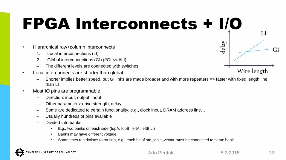
FPGA Interconnects + I/O
• Hierarchical row+column interconnects
1. Local interconnections (LI)
2. Global interconnections (GI) (#GI << #LI)
– The different levels are connected with switches
• Local interconnects are shorter than global
– Shorter implies better speed, but GI links are made broader and with more repeaters => faster with fixed length line
than LI
• Most IO pins are programmable
– Direction: input, output, inout
– Other parameters: drive strength, delay…
– Some are dedicated to certain functionality, e.g., clock input, DRAM address line…
– Usually hundreds of pins available
– Divided into banks
• E.g., two banks on each side (topA, topB, leftA, leftB…)
• Banks may have different voltage
• Sometimes restrictions to routing, e.g., each bit of std_logic_vector must be connected to same bank
5.2.2018Arto Perttula 12
dela
y
Wire length
GI
LI
Arto Perttula 13
Clock Networks in FPGAs
• FPGAs are designed for synchronous logic
– This is the case with 99% of FPGAs even if some exotic devices exist
• FPGAs include clock networks and support different clock domains within the device
• Clock networks are hierarchical
1. Global clocks (Gclk)
2. Regional clocks (Rclk) (may have several)
– Number of Rclk >> Gclk (e.g., 100 Rclks and 16 Gclks)
• Gclks provide a zero-skew clock network spanned over the whole chip
• Rclks provide a zero-skew network within some portion of the chip
– Naturally, all the blocks using given Rclk must reside in same portion
• Someone should tell that to the EDA tools also…
5.2.2018Arto Perttula 14

Generating Clocks
• The mystical ”clk” signal is generated by
a) Input (crystal) oscillator
– Input to the FPGA device (dedicated pins) which buffers the signal
– This can be directly used
b) DLL/PLL circuitry that multiplies/divides the input clock
– Locks to the required frequency, may provide phase shift
– E.g., create a stable 200 MHz clock from 50 MHz input clock
c) Internal feedback-loop clocks or clock dividers
– The most hazardous way
– Doable, but don’t use this
• Prone to variations on process, voltage, and temperature
• Static timing analysis often cannot be used (verification very difficult)
• Place-and-route may change timing (exact timing cannot be set by tools)
• The pulse width will change if you migrate to a different device
5.2.2018Arto Perttula 15

FPGA CONFIGURATION
There are 3 main types of devices
5.2.2018Arto Perttula 16
FPGA Devices 1: SRAM-Based
• SRAM is used to configure the interconnection switches and LUTs
• Majority of FPGAs nowadays
• Usually implemented with leading-edge technology
• Can be re-programmed arbitrarily many time
– Ideal for prototyping and rapid development
• Since SRAMs lose their contents when powered off, an external device (+non-volatile
memory) is required to program them during boot-up
• One concern is security: the device configuration bitstream can be copied during the
programming
– Bitstream encryption can prevent this
• Manufacturers include Altera, Atmel, Lucent, and Xilinx
5.2.2018Arto Perttula 17
FPGA Devices 2: Antifuse
• Need a special in-chip programmer circuitry (may be big), but retain the program during shut-down
(non-volatile)
– Fast boot, good security, low power
– One-time programmable (OTP) only
• No need for external circuitry
• They are rad-hard (quite immune to radiation effects)
– Good for, e.g., space applications
• Compared to the SRAM-based with same technology, antifuses have
– Better density (logic gates/mm2)
– Lower interconnect delay – Faster
– BUT! Usually available chips are even several technology generations behind SRAM-counterparts due to
extra processing steps required
• Cancels some of the benefits
• Manufacturers include, e.g., Actel
5.2.2018Arto Perttula 18
FPGA Devices 3: EEPROM/FLASH
• Programming is similar to SRAM-based, but non-volatile
– Both re-programmable and fast boot
• Good security
• EEPROM and FLASH 1-bit cells need two (special) transistors
– Typical 1-bit SRAM implementation requires 6 transistors
– => Smaller cells than in SRAM devices
– Faster, more density
• BUT! Also few generations behind the leading edge
• Some devices integrate small Flash memory but LUT and wire configuration is done
with SRAM
• Manufacturers include, e.g., Actel, Xilinx
5.2.2018Arto Perttula 19
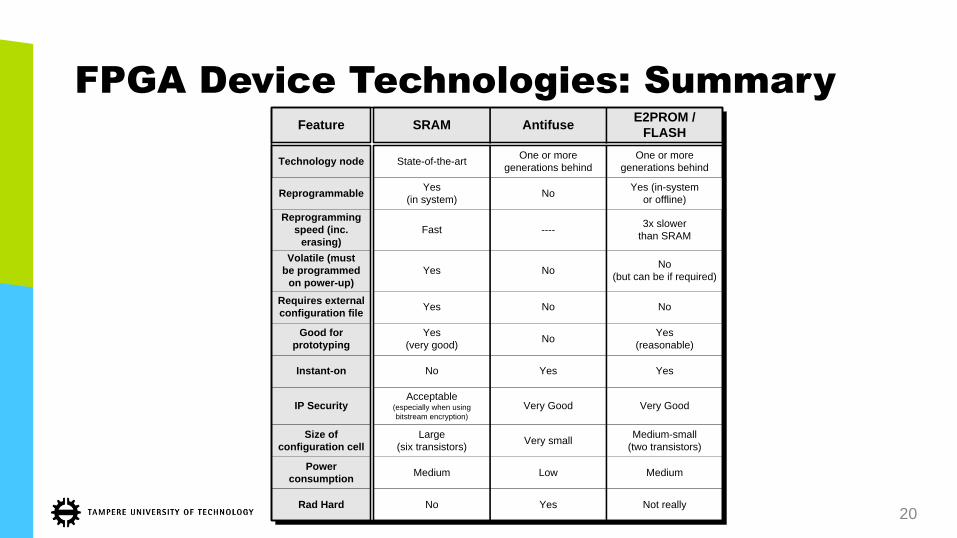
FPGA Device Technologies: Summary
Arto Perttula 20
State-of-the-art
Feature
Technology node
SRAM AntifuseE2PROM /
FLASH
One or more
generations behind
One or more
generations behind
Fast
Reprogramming
speed (inc.
erasing)
----3x slower
than SRAM
Yes
Volatile (must
be programmed
on power-up)
NoNo
(but can be if required)
MediumPower
consumptionLow Medium
Acceptable(especially when using
bitstream encryption)
IP Security Very Good Very Good
Large
(six transistors)
Size of
configuration cellVery small
Medium-small
(two transistors)
NoRad Hard Yes Not really
NoInstant-on Yes Yes
YesRequires external
configuration fileNo No
Yes
(very good)
Good for
prototypingNo
Yes
(reasonable)
Yes
(in system)Reprogrammable No
Yes (in-system
or offline)
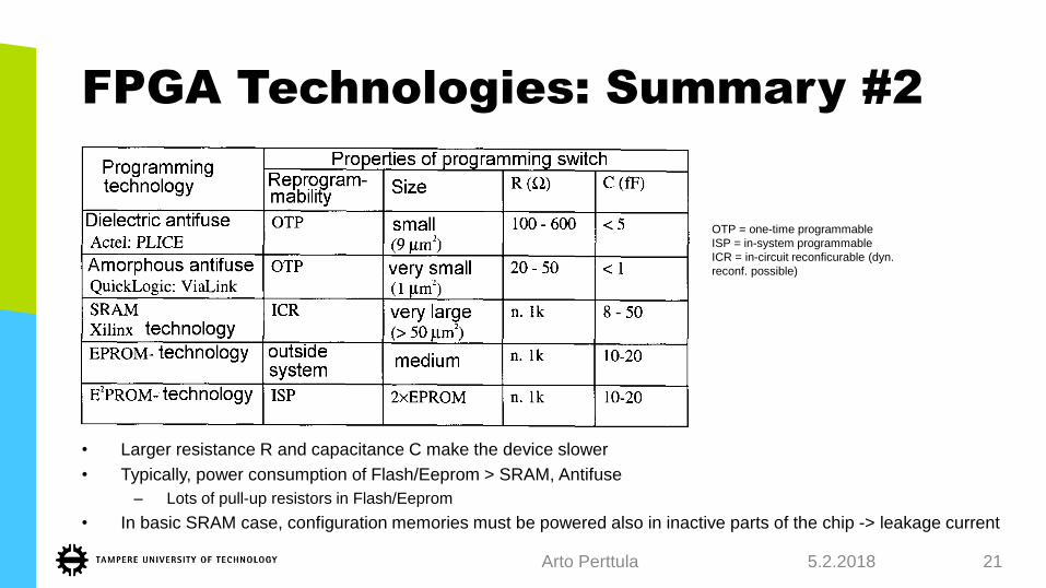
FPGA Technologies: Summary #2
• Larger resistance R and capacitance C make the device slower
• Typically, power consumption of Flash/Eeprom > SRAM, Antifuse
– Lots of pull-up resistors in Flash/Eeprom
• In basic SRAM case, configuration memories must be powered also in inactive parts of the chip -> leakage current
5.2.2018Arto Perttula 21
OTP = one-time programmable
ISP = in-system programmable
ICR = in-circuit reconficurable (dyn.
reconf. possible)

Configurable SRAM-Based FPGA
• The device needs a programming file (also called as bit file or bitstream)
– Includes the programming into for each cell of the FPGA
– Usually proprietary format
• Again, a lot of variation accross manufacturers and devices
• Each cell and interconnection needs to be configured at start-up
– Programming file size from several kilobytes to megabytes
– Takes time in the order of milliseconds or more
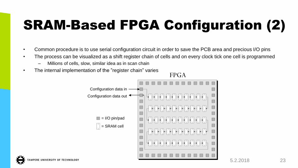
SRAM-Based FPGA Configuration (2)
• Common procedure is to use serial configuration circuit in order to save the PCB area and precious I/O pins
• The process can be visualized as a shift register chain of cells and on every clock tick one cell is programmed
– Millions of cells, slow, similar idea as in scan chain
• The internal implementation of the ”register chain” varies
5.2.2018 23
Configuration data in
Configuration data out
= I/O pin/pad
= SRAM cell
FPGA

SRAM-Based FPGA Configuration (3)
• FPGAs may support also master-mode in which the FPGA may directly
connect to a memory to obtain its configuration bits
– Does not need an external configuration device
• Also parallel programmers are used in order to increase the programming
speed
– Byte-wide ports are common
• JTAG-port is also supported
– Standard connection originally for testing
– Has room for special commands
– Widely used in prototyping phase as the FPGA may be directly programmed with
JTAG, instead of programming the flash and then reseting the device
5.2.2018Arto Perttula 24
Dynamically Reconfigurable Logic
• A design that can be reconfigured on the fly while remaining resident in the
system
– For example, during startup FPGA first performs self-testing
– Then, the real configuration is loaded
• It would be superb that, e.g., a GPS hardware could be reconfigured to
video codec on-the-fly as the user selects that
25
AUDIO VIDEO
Mem Comm
Watching Top Gun movie Tracks down the route to Moscow
AUDIO GPS
Mem Comm
Dynamic partial
reconfigure
Problems in Dynamic Reconfiguration…
• The time it takes to reconfigure the logic and interconnects
– They are typically programmed using a serial data stream (or a parallel stream
only 8 bits wide)
– Usually at least several milliseconds for partial reconfiguration
– Only a few devices support partial reconfiguration (coarse-grain, column-wise)
• The remainder of the device has to be halted
• Layouts of parts must be compatible
• More non-volatile memory required for bitstream
• Reconfigurability was a big fuzz in 1990s and again rising its head
• Not really used yet (currently pretty much PMT*)
5.2.2018Arto Perttula 26
* paljon melua tyhjästä

HARD MACROS AND
GIGABIT TRANSCEIVERS
Transceiver is a device that has both a transmitter and a receiver
which are combined and share common circuitry
5.2.2018Arto Perttula 27
Integrated Hard Macros
• The devices have increasing number of integrated hard macros
– Not built from LUTs (much faster and smaller)
– Included in each device despite of usage everyone pays
– Includes the most common functions
– Allow some configuration even if they are “hard”
• E.g.,
– PLL/DLLs for clock manipulation
– Memories
– High-speed multipliers with accumulate (MAC)
– Integrated microprocessors (e.g., ARM, PowerPC)
– High speed I/O link controllers
5.2.2018Arto Perttula 28
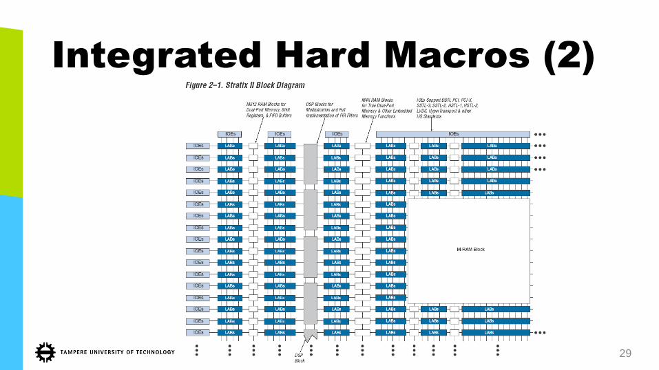
Integrated Hard Macros (2)
5.2.2018Arto Perttula 29
Basics for I/O Transceivers
• Parallel buses have long been the prevailing data transmission type, but high-speed parallel
wiring is very hard to manage
– Signal integrity issues (crosstalk, susceptibility to noise etc., track length on PCB)
• Serial communication simplifies many things
– Unidirectional point-to-point links, only two devices instead of multi-master (compare to shared bus)
– Necessitates higher frequency than parallel communication
5.2.2018 30
FPGA
Differential
pairs
Transceiver block
Transmit (TX) to other device
Receive (RX) from other device

Differential Signaling
• Only the difference between the signal levels matter
– Always carry complementary values
• If the tracks are close to each other, noise will affect both lines similarly the difference stays the
same
31
IN
Standard
Input
Differential
PairRXN
RXP
FPGAOutside
World
IN
RXN
RXP
0
1
Noise spikes
Noise spikes
0
1
(a) (b)
Traditional
Differential

Standards
• Electronics wouldn’t be electronics if there weren’t variety of standards for
this sort of thing:
– Fibre Channel
– InfiniBand
– PCI Express (started and pushed by Intel Corporation)
– RapidIO
– SkyRail (from Mindspeed Technologies)
– 10-gigabit Ethernet
– and others…
• An embedded FPGA transceiver can typically be configured to support
some of these (but not all)
5.2.2018Arto Perttula 32

Integrated Gigabit Transceivers
• E.g., Stratix 3 supports speeds up to 1.25 Gbps
– Fastest implementations are 3-4x faster
• However, we can group a set of transceivers so we can further improve the data rate
– Using 8 transceivers would result in, e.g., 10 Gbps speed
– Extra logic required to pack and unpack the data being send from device to device
• One should try to utilize the FPGA board’s capabilities as much as possible instead of
developing own proprietary solutions
• Sidenote: e.g., 4 Gbps serial link => data transfer rate 4 GHz = 0.25 ns period
– Speed of light is 299,792,458 m/s. Light traverses 7.5 cm during one period, electrons
somewhat less…
5.2.2018Arto Perttula 33
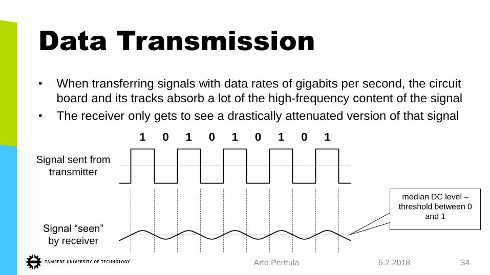
Data Transmission
• When transferring signals with data rates of gigabits per second, the circuit
board and its tracks absorb a lot of the high-frequency content of the signal
• The receiver only gets to see a drastically attenuated version of that signal
5.2.2018Arto Perttula 34
Signal sent from
transmitter
Signal “seen”
by receiver
1 0 1 0 1 0 1 0 1
median DC level –
threshold between 0
and 1

Data Transmission (2)
• Problems arise if you send data that have, e.g., multiple 1’s in the beginning (overly pessimistic example)
• Received signal level constantly over the threshold
• Receiver only sees a chain of 1’s!
• => encoding standards, e.g., 8/10, we send 2 extra bits for each 8 bots to ensure that there is no more than five
0’s or 1’s in a row
– 1/5 of the bandwidth is wasted but DC level will be correct
• Another choice would be lower frequency
5.2.2018Arto Perttula 35
Signal sent from
transmitter
Signal “seen”
by receiver
1 1 1 0 1 0 1 0 1
FPGA PERFORMANCE AND
SELECTION CRITERIA
5.2.2018Arto Perttula 36
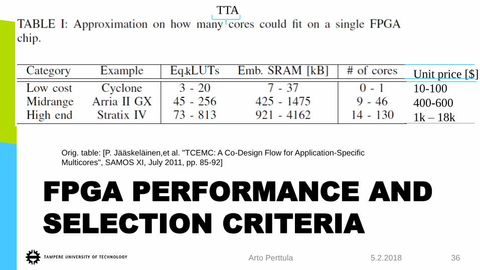
k Unit price [$]
10-100
400-600
1k – 18k
Orig. table: [P. Jääskeläinen,et al. "TCEMC: A Co-Design Flow for Application-Specific
Multicores", SAMOS XI, July 2011, pp. 85-92]
TTA

When to Use FPGAs?
• In large ASIC, NRE (total cost of the design, from initial specification
to PG tape) ranges from 5M$ to 50M$ for a completely new complex
chip using 0.13 micron technologies
– This implies that a chip that will be sold for $5 (with 20% profit) needs
volumes of 5 to 50 million chips to break even!
– …and the cost is getting higher with introduction of new technologies
• If higher profit can be obtained, that naturally lowers the break-even
point
• FPGAs are currently better for volumes under 100K chips/year
– If required performance is obtainable with FPGAs
37Chips of the future: Soft, Crunchy or Hard?, Pierre G. Paulin (organizer and moderator), Date 2004

Typical Application Domains
ASIC:
– Mass products, consumer electronics
– Mobile phones
– Computers
– MP3-players
– Digital cameras
FPGA:
– Industrial (/military) electronics
– Some consumer products (e.g., DVB)
– Cell phone base stations
– Factory automation
– Internet routers
– ”Glue logic”F-16 AN/APG-68
Programmable Signal Radar
Processor uses Altera Stratix II
Mars rover project used
Actel and Xilinx FPGAs
See also: http://www.altera.com/corporate/cust_successes/customer_showcase/view_industry/csh-vindustry.jsp

Tools
• You need a simulator, synthesizer, place-and-route, timing analyzer, and programmer
– In practice, also virtual logic analyzer and design viewers (schematic, RTL, technology, chip level) are
invaluable
• The basic set of tools is provided by the FPGA vendor
• Typically these have sufficient features and are good enough
• Most of all, they’re cheap!
• Development boards can be obtained fairly cheaply (~few hundred to few thousand $)
• The major players like Mentor, Synopsys, and Cadence also offer tools for synthesis (and recently
for physically aware synthesis also)
– May have extra features / better performance
– Not necessarily required
5.2.2018Arto Perttula 39
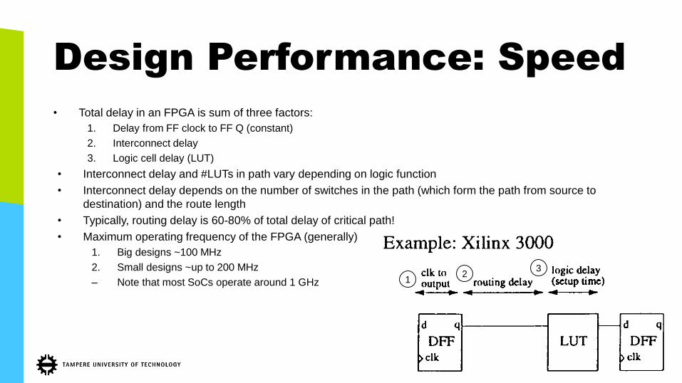
Design Performance: Speed
• Total delay in an FPGA is sum of three factors:
1. Delay from FF clock to FF Q (constant)
2. Interconnect delay
3. Logic cell delay (LUT)
• Interconnect delay and #LUTs in path vary depending on logic function
• Interconnect delay depends on the number of switches in the path (which form the path from source to
destination) and the route length
• Typically, routing delay is 60-80% of total delay of critical path!
• Maximum operating frequency of the FPGA (generally)
1. Big designs ~100 MHz
2. Small designs ~up to 200 MHz
– Note that most SoCs operate around 1 GHz
5.2.2018 40
12
3

Design Performance: Area
• Very dependent on the application
– FPGA is good for register-heavy designs
• The more area the design takes, more difficult it is to route
less clock frequency
• Largest high-end FPGAs can hold very complex architectures,
comprising several soft RISC processors and other hardware
– ”Multi-million ASIC gates”
• Design with small area can be fitted into cheaper FPGA
• 3rd basic measure, power, getting more important
5.2.2018Arto Perttula 41

Separation of Targets
• Strong separation between high-end and low-end FPGA devices
1. Low-end
– Low cost, lower logic capacity, less memory, less integrated hard macros
– Target is the traditional cost-sensitive consumer products and glue-logic domain with possible fancy features, such
as single simple soft processor
– Price from few to tens of euros, cheaper for high quantities
2. High-end are highly optimized, usually for speed and large capacity
– Pricing thousands of euros/device, up to 10k-range for the best (depends again on the volume)
– Target is the traditional ASIC domain
– When high performance is required but not enough products are manufactured to compensate for ASIC’s higher
NRE costs
3. Emerging trend is also to offer structured ASIC of the design
– The design of an FPGA is ”burned” into a structured ASIC that cannot be re-programmed. Altera calls this ”hard-
copy” and Atmel uses term ”ULC”.
– Saves power and area, increases speed due to removal of the programming resources
– EETimes: power -40%, area -70%, performance +50-100%, price -30%
42[http://www.eetimes.com/electronics-news/4124922/Altera-Unveils-HardCopy-for-Stratix]
[http://www.altera.com/products/devices/hardcopy-asics/about/migration/hrd-migration.html]

Hard-Copy FPGA
5.2.2018 43
Figure: [V. Betz, "Will Power Kill
FPGAs?," ACM/SIGDA International
Symposium on FPGAs, Monterey, CA,
2006]
http://www.eecg.toronto.edu/~vaughn/p
apers/fpga2006_power_panel.pdf
Table: [Generating Functionally
Equivalent FPGAs and ASICs With a
Single
Set of RTL and Synthesis/Timing
Constraints, Altera white paper, WP-
01095-1.2, February 2009, ver. 1.2]
NRE reduced from ASIC, e.g. by 2x -3x and consequently the cost break-even between FPGA and
hard-copy might be as low as 5k-10k units .[programmablelogicZONE Products for the week of May 19, 2008, http://www.en-
genius.net/site/zones/programmablelogicZONE/product_reviews/plp_051908]
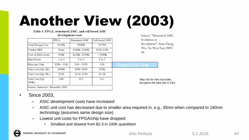
Another View (2003)
• Since 2003,
– ASIC development costs have increased
– ASIC unit cost has decreased due to smaller area required in, e.g., 65nm when compared to 180nm
technology (assumes same design size)
– Lowest unit costs for FPGA/chip have dropped
• Smallest and slowest from $2-3 in 100K quantities!
5.2.2018Arto Perttula 44
Source: “Structured ASIC,
Evolution or
Revolution?”, Kun-Cheng
Wu, Yu-Wen Tsai, ISPD
04
Suspicious line…
May not be very accurate,
but gives the idea (for 0.13u)
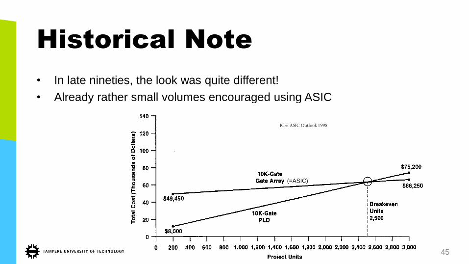
Historical Note
• In late nineties, the look was quite different!
• Already rather small volumes encouraged using ASIC
5.2.2018Arto Perttula 45
ICE: ASIC Outlook 1998
(=ASIC)
FPGA Device Selection Criteria #1
1. Circuit capacity
– Amount of logic elements and registers, logic element size, (routing resources)
– Amount of RAM, types of RAM
– Required hard macros
– I/O signal routing (How the location of an I/O pin affects the routing)
2. Number of I/O signals and supported standards
3. Pricing
– Unit price in volume production
– Development cost
– Ranges a lot depending on the amount, specific device and package (and the client)
– Prices are subject to rapid changes long term contracts should be carefully considered
– FPGAs are rather expensive, e.g., 5-150 euros, and cheapest microcontrollers are ~0.95-5 euros
4. Temperature range, radiation-hardness
5. Power consumption
5.2.2018Arto Perttula 46
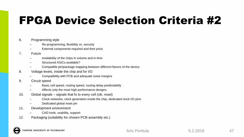
FPGA Device Selection Criteria #2
6. Programming style
– Re-programming, flexibility vs. security
– External components required and their price
7. Future
– Availability of the chips in volume and in time
– Structured ASICs available?
– Compatible pin/package mapping between different flavors of the device
8. Voltage levels, inside the chip and for I/O
– Compatibility with PCB and adequate noise margins
9. Circuit speed
– Basic cell speed, routing speed, routing delay predictability
– Affects only the most high-performance designs
10. Global signals – signals that fo to every cell (clk, reset)
– Clock networks, clock generation inside the chip, dedicated clock I/O pins
– Dedicated global reset pin
11. Development environment
– CAD tools, usability, support
12. Packaging (suitability for chosen PCB assembly etc.)
5.2.2018Arto Perttula 47

Availability and Life Span
• The digital CMOS technology develops rapidly
– New devices are introduced faster and faster
• The life span of certain device is dictated by its demand
– Widely used devices are more certain to stick around for years
– Very widely used devices may life quite long (even 10 years, e.g., Xilinx XC3000, Altera Flex 10k)
• The old device may be convertible to a new device without modifications
– Package, pins, operating voltage, configuration
– Operating voltage tends to change between technology generations and that causes most of the problems
with compatibility
• The manufacturer may give some guarantees of life span
• Choosing between different vendors may be complicated. The experience with certain
manufacturers devices may be the dominant factor.
• Relying purely on soft, FPGA-vendor-independent IP cores, helps in porting the system to another
device
5.2.2018Arto Perttula 48
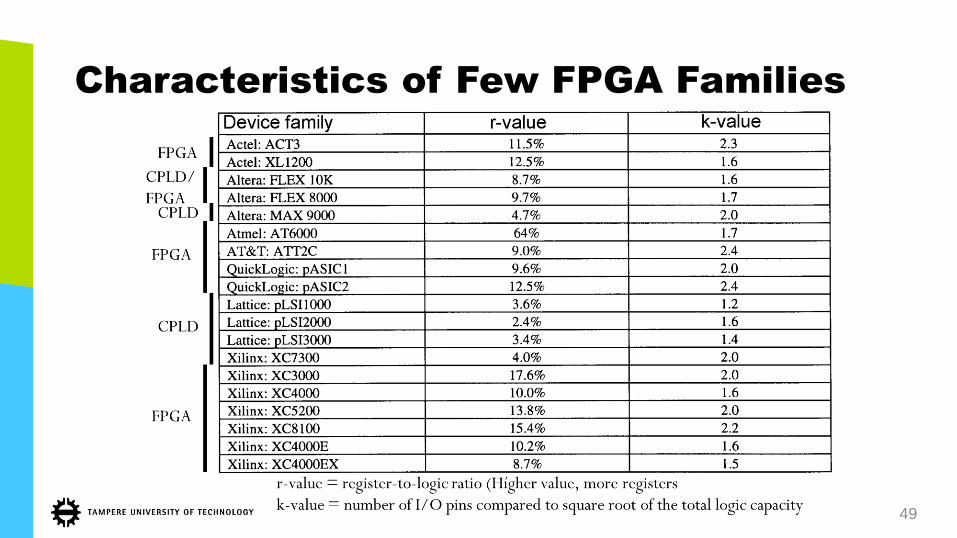
Characteristics of Few FPGA Families
49

FUTURE OF FPGAS
5.2.2018Arto Perttula 50
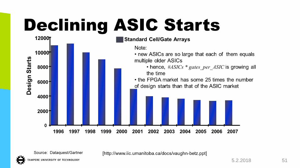
Declining ASIC Starts
5.2.2018 51

Number of Project Starts Per Year
• Roughly +26% growth for FPGA and SoC 2007-2010
– http://www.scdsource.com/article.php?id=3
• Each new generation is more complex than its predecessor
5.2.2018Arto Perttula 52
Possible FPGA Developments
• The FPGA capacity will continue to grow with processing technology
improvements
– 90nm devices at 2004, 65nm at 2006, 2008-2009 45nm, 2010 28nm, 2013 14nm
• Note that this is the first introduction, not volume production
• Partial reconfiguration / faster configuration?
• Widening separation to low-power and high-performance devices
• More hard macros
– A/D and D/A converters are a good guess for next
• FPGA using non-volatile MRAM configuration
– Potential to comprise the speed of SRAM and non-voltility of FLASH
5.2.2018Arto Perttula 53

Possible FPGA Developments (2)
• We might even see considerable changes in the FPGA device architecture
of LEs and interconnects
– > 10 years the basic LE contained 4-input LUT and flip-flop
– This has changed in 2005 to 6-8-input LUT and 2 flip-flops
– Solution to reduce routing overhead vs. logic delay is increasingly important
• ”Field Programmable Node Arrays”, Coarse grain reconfiguration?
– The FPGAs would consist of nodes that are large programmable functional
blocks such as algorithmical accelerators or CPUs (the mode can be configured)
– Adder, MUL, register file, small ALU… instead of LUT+FF
– These nodes are interconnected with hierarchical networks
5.2.2018Arto Perttula 54
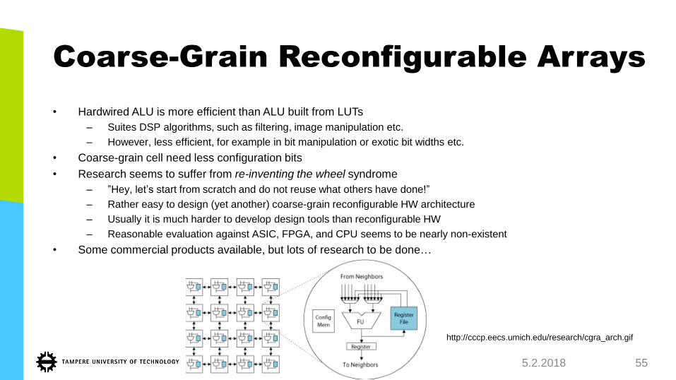
Coarse-Grain Reconfigurable Arrays
• Hardwired ALU is more efficient than ALU built from LUTs
– Suites DSP algorithms, such as filtering, image manipulation etc.
– However, less efficient, for example in bit manipulation or exotic bit widths etc.
• Coarse-grain cell need less configuration bits
• Research seems to suffer from re-inventing the wheel syndrome
– ”Hey, let’s start from scratch and do not reuse what others have done!”
– Rather easy to design (yet another) coarse-grain reconfigurable HW architecture
– Usually it is much harder to develop design tools than reconfigurable HW
– Reasonable evaluation against ASIC, FPGA, and CPU seems to be nearly non-existent
• Some commercial products available, but lots of research to be done…
5.2.2018Arto Perttula 55
http://cccp.eecs.umich.edu/research/cgra_arch.gif

STRATIX III FPGA
Real-life example
5.2.2018Arto Perttula 56
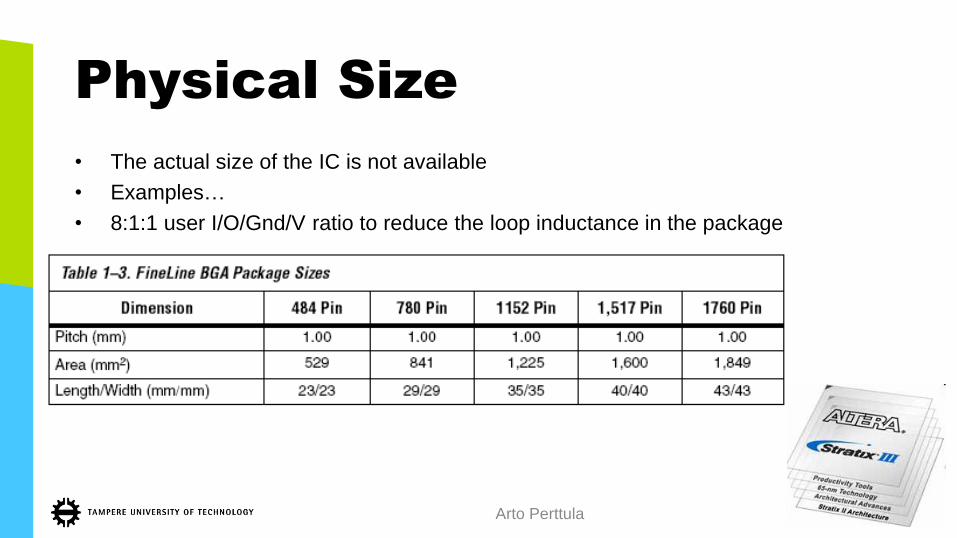
Physical Size
• The actual size of the IC is not available
• Examples…
• 8:1:1 user I/O/Gnd/V ratio to reduce the loop inductance in the package
Arto Perttula 57

Altera Stratix III Architecture
58

Logic Array Block (LAB)
• Each Logic Array Block (LAB) consists of ten Adaptive Logic Modules (ALM) + interconnection lines
• Some LABs can be implemented as Memory LAB (MLAB)
– ALM is used as 64x1 or 32x2 RAM block
• LABs may perform in low power or high performance mode, the synthesis tool automatically sets non-critical paths
to low power and vice versa
5.2.2018Arto Perttula 59
Source:
http://www.altera.com/products/devices/stratix3/
overview/power/st3-power.html

ALM Contents
• ALM operating modes
1. Normal
2. Extended LUT mode
3. Arithmetic
4. Shared Arithmetic
5. LUT-Register
• There are 8 general-purpose data inputs, carry in and shared arithmetic
connector from previous ALM or LAB, and register chain connection
• LAB-wide signals
– Clock, async clear, sync clear, synch load, clock enable
5.2.2018Arto Perttula 60

High-Level Block Diagram of
the Stratix III ALM
5.2.2018Arto Perttula 61
Fig 2-5
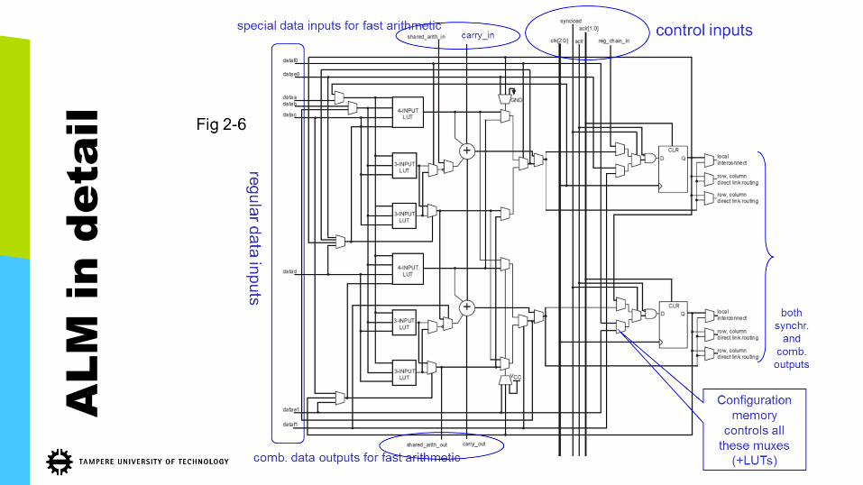
AL
M in
d
etail

ALM Modes: Normal
• Suitable for general logic
applications and
combinational functions
• 8 inputs
a) Any function up to 6 inputs
b) Combination of two
smaller functions
5.2.2018Arto Perttula
ALM Modes
• Usually dictated by the synthesis software and does not need
manual tweaking
• Other than normal mode can be used to implement special
structures, such as fast arithmetics
– Circuits that need a lot of arithmetic, e.g., all the counters and
comparators
• Extended LUT mode allows specific set of 7-input functions to be
implemented (a mux-function)
• LUT-register mode forms one DFF from the 2 LUTs of ALM (so the
ALM has 1+2=3 flip-flops)
5.2.2018Arto Perttula 64
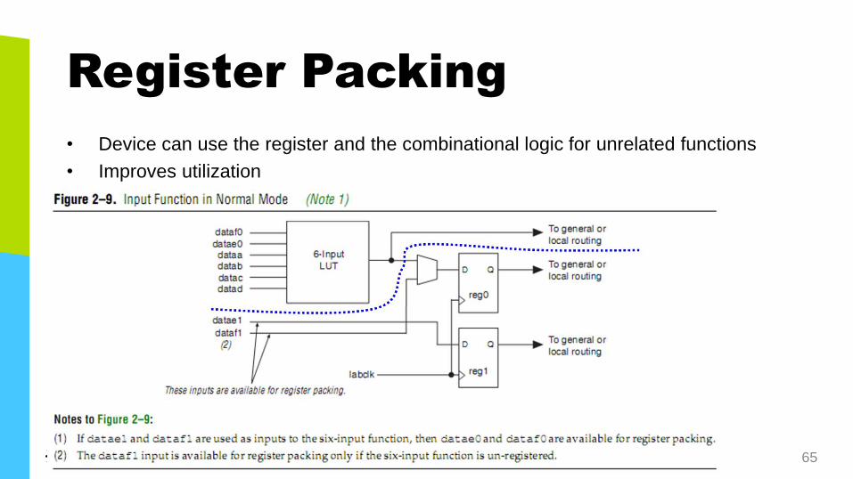
Register Packing
• Device can use the register and the combinational logic for unrelated functions
• Improves utilization
5.2.2018Arto Perttula 65

Hard Macros: TriMatrix Memory
• Configurable, fast (up to 600MHz) on-chip SRAM memories
• Various bit widths supported, can be grouped together to form different sized
memories
5.2.2018Arto Perttula 66
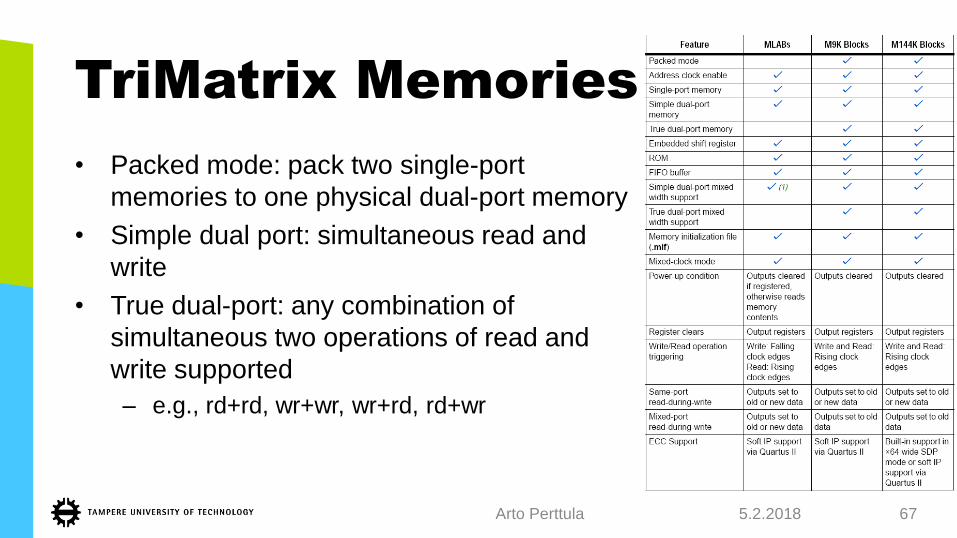
TriMatrix Memories
• Packed mode: pack two single-port
memories to one physical dual-port memory
• Simple dual port: simultaneous read and
write
• True dual-port: any combination of
simultaneous two operations of read and
write supported
– e.g., rd+rd, wr+wr, wr+rd, rd+wr
5.2.2018Arto Perttula 67
Hard Macros: DSP Blocks
• High-performance, power-optimized, fully registered and pipelined multiplication
• Number of DSPs range from 27 to 112 (>54 36x36 multipliers or more)
– Not to be confused with DSP processors…
• Natively supported
– 9-bit, 12-bit, 18-bit, 36-bit word lengths
– 18-bit complex multiplications
– Floating-point arithmetics: 24-bit for single precision and 53-bit for double precision
– Signed and unsigned input support
• Built-in addition, subtraction and accumulation units to combine multiplication results
• Cascading 18-bit input bus to form tap-delay line for filtering applications
• Cascading 44-bit output bus to propagate output results from one block to the next block without
external logic support
• Rich and flexible arithmetic rounding and saturation units
• Efficient barrel shifter support, loopback capability for adaptive filtering
5.2.2018Arto Perttula 68
INTERCONNECTS
5.2.2018Arto Perttula 69
Interconnect Types
1. Local
– Between LABs and adjacent blocks (20 links)
2. R4
– Traversing four blocks to the right or left
– Span a combination of four LABs, Memories, or DEP blocks
3. R20
– Span over 20 LABs
– High-speed accross the device routing (cascaded)
4. C4
– Four blocks up/down in the same device column
5. C12
– Connect 12 LABs
– High-speed vertical routing links through the device
5.2.2018Arto Perttula 70
LAB Interconnect
• The 10 ALM within LAB are
connected with local interconnect
• Moreover, there are three
dedicated paths between ALMs:
1. Register Cascade – for a fast
shift register
2. Carry-chain – for fast
addition/subtraction
3. Shared Arithmetic chain – for
fast adder trees
5.2.2018 71
R4 Interconnect
Arto Perttula 72

C4 Interconnect
• Spans 4 interfaces in
the same column
– 4 LABs
– 1 DSP block
– ½ M144K memory
• LAB may drive C4 both
on its left and right side
Arto Perttula 73From fig 3-3
...
...

Cascading the Links
• The links can naturally be cascaded
• E.g., R4 can connect to R4 or C4, as also C4
• Number of reachable LABs grows very fast
• Quartus automatically places critical design paths on faster
interconnects
5.2.2018Arto Perttula 74

DSP Blocks
• A DSP block is divided into four blocks
– Interface with four LAB rows on the left
and right
• Can be cascaded by fast local links
• One DSP block corresponds to roughly
60-100 LEs, depending on parameter
widths and types
5.2.2018Arto Perttula 75

M9K Memory Routing
5.2.2018Arto Perttula 76
9 Kbit

M144K Memory Routing
5.2.2018Arto Perttula 77
144 Kbit

5.2.2018Arto Perttula 78
Ro
utin
gS
ch
em
e

CLOCKS, PLL’S, AND
INPUT/OUTPUT
5.2.2018Arto Perttula 79

Clock Resources
• The clock networks are zero-skew networks (i.e., heavily buffered and delay-compensated)
• The clock lines can also be used to drive other high-fanout signals such as device-wide reset
5.2.2018 80(notes 1-4) : depends on device type
Global and Regional Clock Networks
• Global clocks can be used to drive logic and other blocks throughout the device
– 16 GCLKs
• Regional clocks can only be used in one device quadrant
• Only certain input pins can be connected to clock network
5.2.2018 81
Periphery Clock Networks
• Periphery clock (PCLK) networks are a collection of individual clock
networks driven from the periphery of the Stratix II device
• Clock outputs from the dynamic phase aligner (DPA) block,
horizontal I/O pins, and internal logic can drive the PCLK networks
– DPA is for I/O
• These PCLKs have higher skew compared to GCLK and RCLK
networks
• Can be used instead of general purpose routing to drive signals into
and out of the Stratix III device
• Avoid using these if not sure what these are for 5.2.2018Arto Perttula 82
Clock Sources
a) Stratix III logic can be driven directly by the external clocks
b) Configurable PLLs can generate a wide range of frequencies
– PLL = phase-locked loop
– Very useful special components
– Up to 12 PLLs in Stratix III
c) User logic in LAB
• Clock signals can be disabled to save power
5.2.2018Arto Perttula 83
PLL Properties
• Main goal of a PLL is to synchronize the phase and frequency of an internal or
external clock to an input reference clock
• Counters for divide and multiplication to get required frequency
– E.g., 50 MHz clk*2/3 33 MHz clk
– Parameters m and n in range 1-512 (f_out = f_in*m/n)
• Lock time: how long it takes to get the required frequency stabilized (~1ms)
• Jitter: how much the duty cycle/frequency varies
– E.g., cycle-to-cycle jitter: two consecutive cycles’ periods differ at mist by 17.5 ps
– E.g., period jitter: with 99.99% probability clock edge time differs at most by ±175 ps from
ideal clock (when measured over 10k cycles)
• Duty cycle: up/down times (e.g., 50/50)
• Phase shift: relation between input and output clock edges
5.2.2018Arto Perttula 84
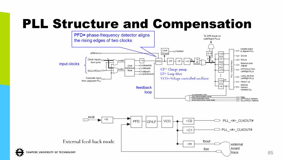
PLL Structure and Compensation
5.2.2018Arto Perttula 85
Input/Output Pins
• The way to interface external components, such as displays, buttons, and
memories
• Number of I/O pins depend on the package and device
– 296-1120 user I/O pins available in Stratix III
– Many pins are required for voltage and ground (not accounted in the above)
• A pin can be in, out, or three-stated (programmable)
• Stratix device also includes dynamic series and parallel on-chip termination
to provide I/O impedance matching and termination capabilities
• The I/Os are configurable and support a wide range of standards
5.2.2018Arto Perttula 86
I/O Standards and Properties
• Single-ended, non-voltage-referenced and voltage-referenced I/O standards
• Low-voltage differential signaling (LVDS), reduced swing differential signal (RSDS), mini-LVDS, high-speed
transceiver logic (HSTL), and stub series terminated logic (SSTL)
• Single data rate (SDR) and half data rate (HDR – half frequency and twice the data width of SDR) input and output
options
• Up to 132 full duplex 1.25 Gbps true LVDS channels (132 Tx + 132 Rx) on the row I/O banks
• Hard DPA block with serializer/deserializer (SERDES)
• De-skew, read and write leveling, and clock-domain crossing functionality
• Programmable
– output current strength, e.g., 4-16 mA/pin
– slew rate – how fast voltage changes, e.g., 50 Volt/µsec
– delay, e.g., 0-1000 ps
– bus-hold – keeps the state of three-state bus until someone drives it
– pull-up resistor – provides default value if no-one drives, e.g., 25 kΩ
– Hysteresis/toggle point
• Open-drain output
5.2.2018Arto Perttula 87

Supported I/O Standards and
Applications
5.2.2018 88
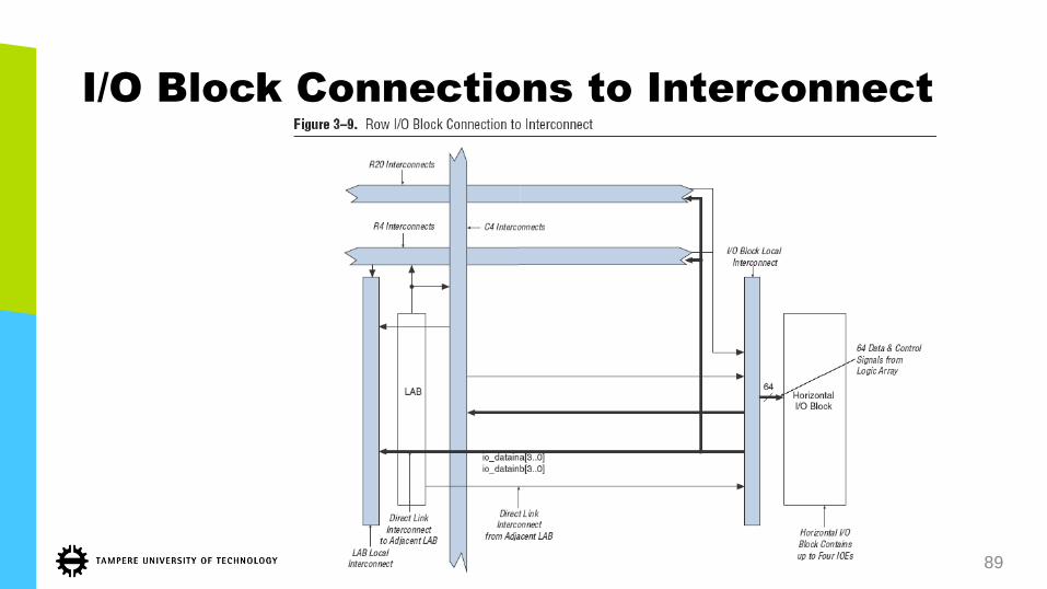
I/O Block Connections to Interconnect
5.2.2018Arto Perttula 89

The I/O Element Structure
5.2.2018Arto Perttula 90
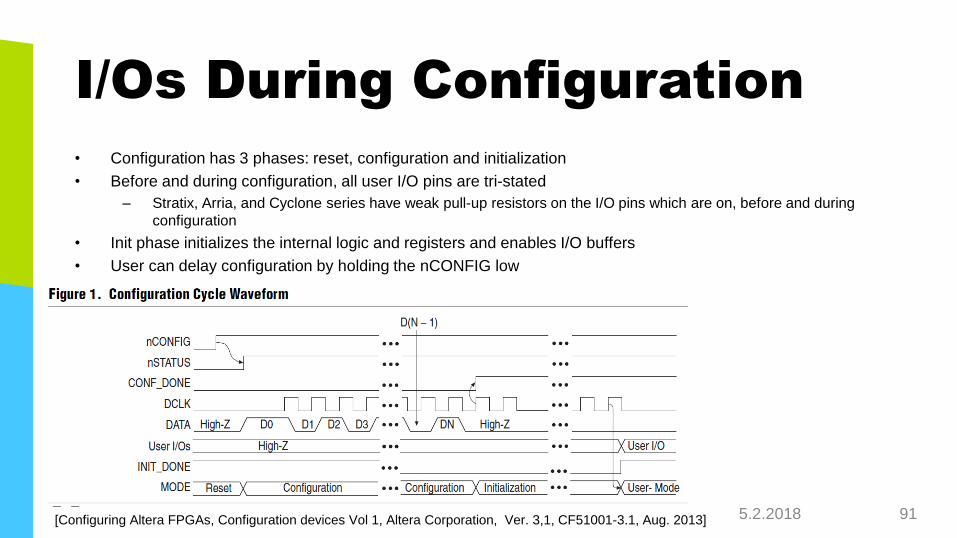
I/Os During Configuration
• Configuration has 3 phases: reset, configuration and initialization
• Before and during configuration, all user I/O pins are tri-stated
– Stratix, Arria, and Cyclone series have weak pull-up resistors on the I/O pins which are on, before and during
configuration
• Init phase initializes the internal logic and registers and enables I/O buffers
• User can delay configuration by holding the nCONFIG low
5.2.2018Arto Perttula 91[Configuring Altera FPGAs, Configuration devices Vol 1, Altera Corporation, Ver. 3,1, CF51001-3.1, Aug. 2013]

Design Security in Stratix III
• Configuration bitstream may be encrypted with 256b AES
– The stream that is stored in the Flash
– Available with only certain device configuration modes
• The key is stored in FPGA device and cannot be read out
– The key is also scrambled
• The configuration-file read-back is not supported
• Tamper Protection bit
– Once set, only bitstream encoded with the certain key may be used to program the FPGA
• Volatile and non-volatile key supported
– Volatile needs an external battery
– Non-volatile is one time programmable (fuses)
5.2.2018Arto Perttula 92
STRATIX FAMILY SUMMARY
5.2.2018Arto Perttula 93
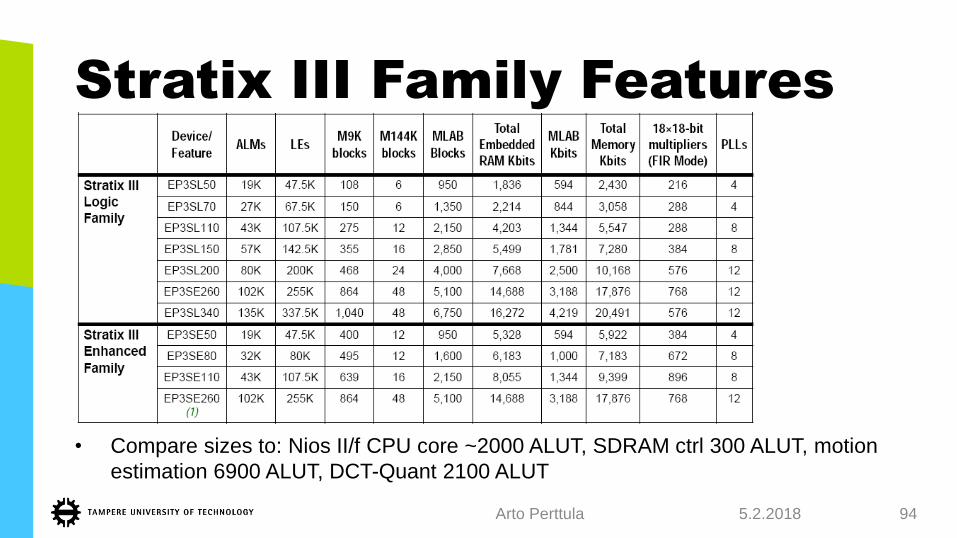
Stratix III Family Features
• Compare sizes to: Nios II/f CPU core ~2000 ALUT, SDRAM ctrl 300 ALUT, motion
estimation 6900 ALUT, DCT-Quant 2100 ALUT
5.2.2018Arto Perttula 94
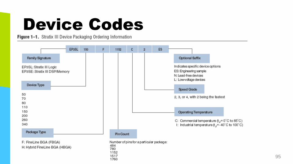
Device Codes
5.2.2018Arto Perttula 95

Maximum Frequencies
5.2.2018Arto Perttula
DSP blocks
Clock tree

Stratix II LAB Parameters
• Stratix II data, did not find for Stratix III
5.2.2018Arto Perttula 97
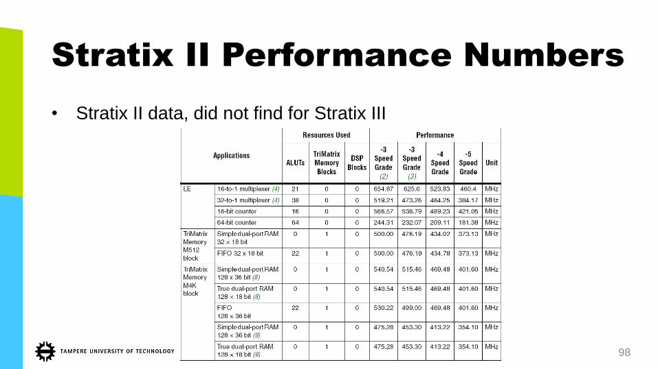
Stratix II Performance Numbers
• Stratix II data, did not find for Stratix III
Arto Perttula 98

Stratix II Embedded Memories
5.2.2018Arto Perttula 99
M9K

INTERFACING EXTERNAL
COMPONENTS
Case study: SDRAM controller
5.2.2018Arto Perttula 100
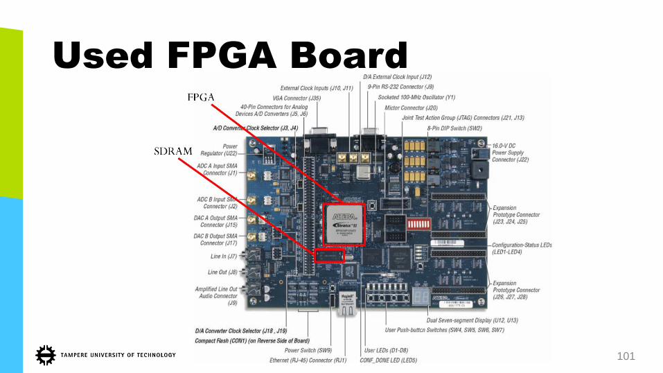
Used FPGA Board
5.2.2018Arto Perttula 101

Requirements in a Nutshell
• SDRAM is synchronous, hence we must provide the clock for SDRAM
• A controller is constructed in FPGA
– Fetches and stores data; refreshes memory periodically
• SDRAM must be usable with configurable frequency up to 133 MHz as well as the
controller
– Requires (static) computation of the timing parameters
• CAS latency (column access latency) increases with frequency
• Required refresh period
• Note the example is specific to sdram chip, FPGA device, and PCB
– Basics apply in general, but one has to adapt the actual values for own environment
5.2.2018Arto Perttula 102

Block Diagram of SDRAM Interfacing
5.2.2018Arto Perttula 103
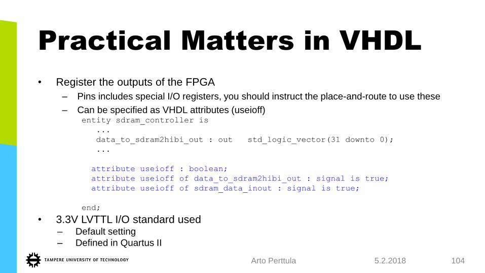
Practical Matters in VHDL
• Register the outputs of the FPGA
– Pins includes special I/O registers, you should instruct the place-and-route to use these
– Can be specified as VHDL attributes (useioff)entity sdram_controller is
...
data_to_sdram2hibi_out : out std_logic_vector(31 downto 0);
...
attribute useioff : boolean;
attribute useioff of data_to_sdram2hibi_out : signal is true;
attribute useioff of sdram_data_inout : signal is true;
end;
• 3.3V LVTTL I/O standard used– Default setting
– Defined in Quartus II
5.2.2018Arto Perttula 104
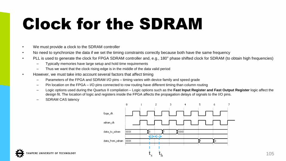
Clock for the SDRAM
• We must provide a clock to the SDRAM controller
• No need to synchronize the data if we set the timing constraints correctly because both have the same frequency
• PLL is used to generate the clock for FPGA SDRAM controller and, e.g., 180° phase shifted clock for SDRAM (to obtain high frequencies)
– Typically memories have large setup and hold time requirements
– Thus we want that the clock rising edge is in the middle of the data valid period
• However, we must take into account several factors that affect timing
– Parameters of the FPGA and SDRAM I/O pins – timing varies with device family and speed grade
– Pin location on the FPGA – I/O pins connected to row routing have different timing than column routing
– Logic options used during the Quartus II compilation – Logic options such as the Fast Input Register and Fast Output Register logic affect the
design fit. The location of logic and registers inside the FPGA affects the propagation delays of signals to the I/O pins.
– SDRAM CAS latency
105ts th

Example SDRAM Timing
5.2.2018 106
Note that required tds and tdh (=ts and th) may have
different duration
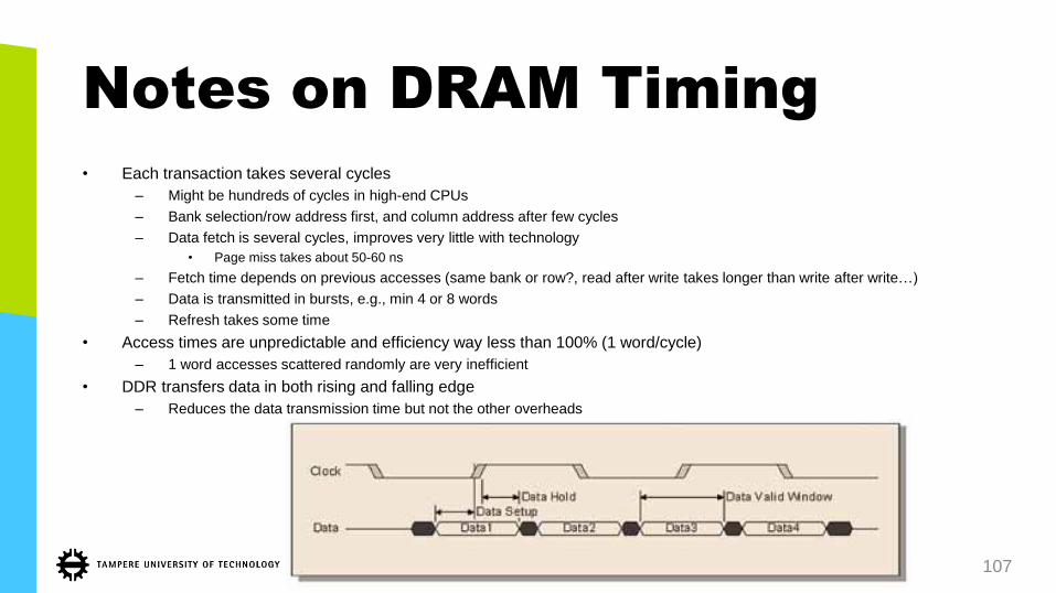
Notes on DRAM Timing
• Each transaction takes several cycles
– Might be hundreds of cycles in high-end CPUs
– Bank selection/row address first, and column address after few cycles
– Data fetch is several cycles, improves very little with technology
• Page miss takes about 50-60 ns
– Fetch time depends on previous accesses (same bank or row?, read after write takes longer than write after write…)
– Data is transmitted in bursts, e.g., min 4 or 8 words
– Refresh takes some time
• Access times are unpredictable and efficiency way less than 100% (1 word/cycle)
– 1 word accesses scattered randomly are very inefficient
• DDR transfers data in both rising and falling edge
– Reduces the data transmission time but not the other overheads
5.2.2018Arto Perttula 107
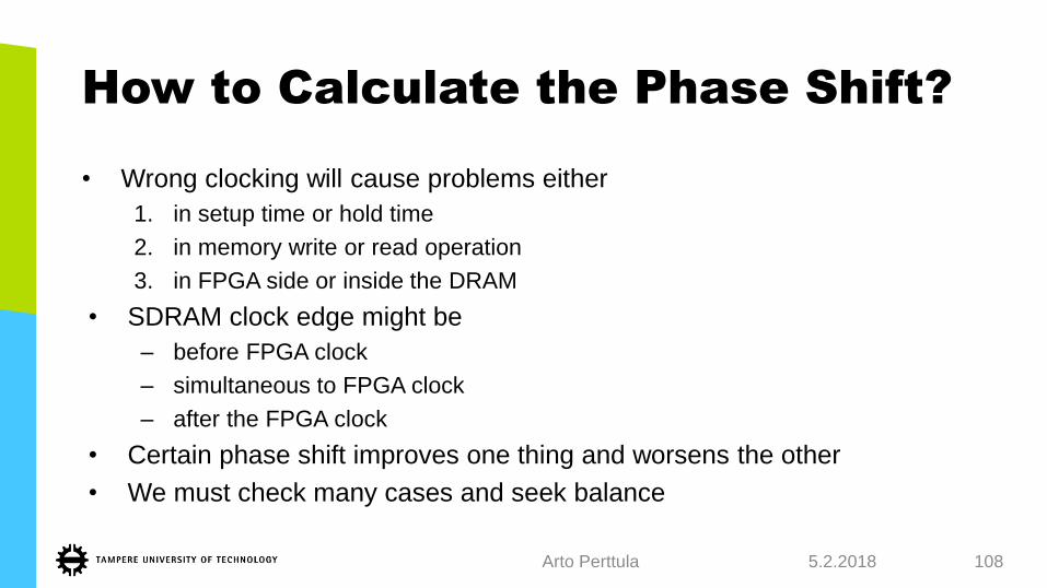
How to Calculate the Phase Shift?
• Wrong clocking will cause problems either
1. in setup time or hold time
2. in memory write or read operation
3. in FPGA side or inside the DRAM
• SDRAM clock edge might be
– before FPGA clock
– simultaneous to FPGA clock
– after the FPGA clock
• Certain phase shift improves one thing and worsens the other
• We must check many cases and seek balance
5.2.2018Arto Perttula 108
Calculate Negative Time Shift
5.2.2018 109

Calculate Positive Phase Shift
5.2.2018Arto Perttula 110
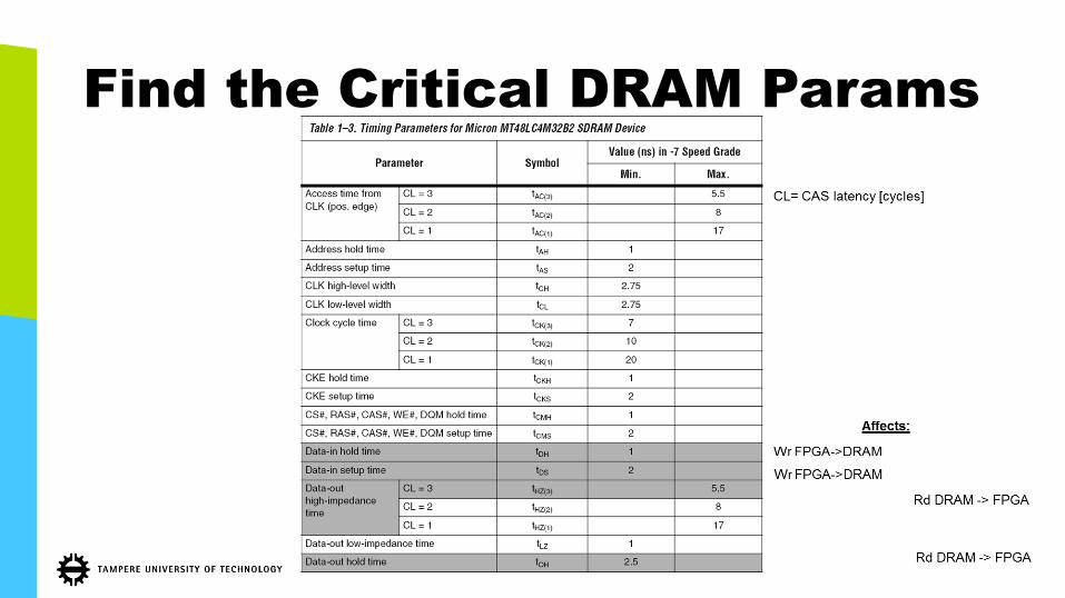
Find the Critical DRAM Params

Find the Critical FPGA Params
• Note that these calculations show an estimate and basic principle only
• The unaccounted (design-specific) parameters are
– Signal skew due to delays on the printed circuit board – These calculations assume zero skew
– Delay from the PLL clock output nodes to destinations – These calculations assume the delay from the PLL
– SDRAM-clock output-node to the pin is the same as the delay from the PLL controller-clock output-node to the clock
inputs in the DRAM controller. If these clock delays are significantly different, you must account for this phase shift in
your window calculations.
5.2.2018Arto Perttula 112
Wr FPGA->DRAM
Affects:
Wr FPGA->DRAM
Rd DRAM -> FPGA
Rd DRAM -> FPGA
How Early Can SDRAM Clock Be?
• How early can SDRAM clock be w.r.t. controller clock
• Select the lesser of Read Lag or Write Lag
Read Lag = tOH(SDRAM)– tH_MAX(FPGA)
Read Lag = 2.5ns –(–5.607ns)
Read Lag = 8.107ns
Write Lag = tCLK – tCO_MAX(FPGA)– tDS(SDRAM)
Write Lag = 20ns – 2.477ns
Write Lag = 17.523ns
• Read lag is smaller: 8.107 ns
• Remember that “lag” is negative with respect to controller clock edge (in Altera terminology)
5.2.2018Arto Perttula 113

How Late Can SDRAM Clock Be?
• How late can SDRAM clock be w.r.t. controller clock
• Select the lesser of Read Lead or Write Lead
Read Lead = tCO_MIN(FPGA)– tDH(SDRAM)
Read Lead = 2.399ns – 1.0ns
Read Lead = 1.399ns
Write Lead = tCLK – tHZ(3)(SDRAM)– tSU_MAX(FPGA)
Write Lead = 20ns – 5.5ns – 5.936ns
Write Lead = 8.564ns
• Read lead is smaller: 1.339 ns
• ”Lead” is positive with respect to controller clock (in Altera terminology)
5.2.2018Arto Perttula 114

Select the Phase Shift
• Read lag: -8.107 ns
• Read lead: 1.399 ns
• Data valid region is thus (read lag to read lead) = -8.107 ns to 1.399 ns
• Safest point is in the middle:
• (-8.107 + 1.399 )÷ 2 = –3.35ns
Phase shift the clock to SDRAM by -3.35 ns
• Clock edge is earlier in SDRAM than in controller
5.2.2018Arto Perttula 115
SDRAM clock
controller clock
20 ns
3.35 ns
Green region highlights the legal phase shifts.
This example ought to work also without phase
shift, but shifting adds tolerance and enhances
dependability
Summary
• And now SDRAM works
– Of course, after this you must use a test block/program that just reads
and writes the memory
– Then you can try out different phase shifts to validate the calculations
• FPGAs
– Built from logic cells (LUT+DFF), hard macros, and routing network
– Excellent for prototypes and small volume products, especially when
many special IOs are needed
– 3 config types: SRAM, antifuse and EEPROM/Flash
5.2.2018Arto Perttula 116