High-frequency programmable acoustic wave device … programmable acoustic wave device realized...
5
High-frequency programmable acoustic wave device realized through ferroelectric domain engineering Yachin Ivry, Nan Wang, and Colm Durkan Citation: Applied Physics Letters 104, 133505 (2014); doi: 10.1063/1.4869823 View online: http://dx.doi.org/10.1063/1.4869823 View Table of Contents: http://scitation.aip.org/content/aip/journal/apl/104/13?ver=pdfcov Published by the AIP Publishing Articles you may be interested in Comprehensive characterization of surface acoustic wave resonators using relaxor based ferroelectric single crystals Appl. Phys. Lett. 103, 032907 (2013); 10.1063/1.4816020 Single ferroelectric domain nucleation and growth monitored by high speed piezoforce microscopy J. Vac. Sci. Technol. B 27, 1011 (2009); 10.1116/1.3077485 High-frequency surface acoustic wave devices based on LiNbO 3 diamond multilayered structure Appl. Phys. Lett. 87, 213503 (2005); 10.1063/1.2135383 High-frequency surface acoustic wave device based on thin-film piezoelectric interdigital transducers Appl. Phys. Lett. 85, 1757 (2004); 10.1063/1.1787897 Quantitative analysis of the bit size dependence on the pulse width and pulse voltage in ferroelectric memory devices using atomic force microscopy J. Vac. Sci. Technol. B 19, 818 (2001); 10.1116/1.1364697 This article is copyrighted as indicated in the article. Reuse of AIP content is subject to the terms at: http://scitation.aip.org/termsconditions. Downloaded to IP: 18.62.11.123 On: Fri, 01 Aug 2014 02:59:54
Transcript of High-frequency programmable acoustic wave device … programmable acoustic wave device realized...

High-frequency programmable acoustic wave device realized through ferroelectricdomain engineeringYachin Ivry, Nan Wang, and Colm Durkan
Citation: Applied Physics Letters 104, 133505 (2014); doi: 10.1063/1.4869823 View online: http://dx.doi.org/10.1063/1.4869823 View Table of Contents: http://scitation.aip.org/content/aip/journal/apl/104/13?ver=pdfcov Published by the AIP Publishing Articles you may be interested in Comprehensive characterization of surface acoustic wave resonators using relaxor based ferroelectric singlecrystals Appl. Phys. Lett. 103, 032907 (2013); 10.1063/1.4816020 Single ferroelectric domain nucleation and growth monitored by high speed piezoforce microscopy J. Vac. Sci. Technol. B 27, 1011 (2009); 10.1116/1.3077485 High-frequency surface acoustic wave devices based on LiNbO 3 diamond multilayered structure Appl. Phys. Lett. 87, 213503 (2005); 10.1063/1.2135383 High-frequency surface acoustic wave device based on thin-film piezoelectric interdigital transducers Appl. Phys. Lett. 85, 1757 (2004); 10.1063/1.1787897 Quantitative analysis of the bit size dependence on the pulse width and pulse voltage in ferroelectric memorydevices using atomic force microscopy J. Vac. Sci. Technol. B 19, 818 (2001); 10.1116/1.1364697
This article is copyrighted as indicated in the article. Reuse of AIP content is subject to the terms at: http://scitation.aip.org/termsconditions. Downloaded to IP: 18.62.11.123
On: Fri, 01 Aug 2014 02:59:54

High-frequency programmable acoustic wave device realized throughferroelectric domain engineering
Yachin Ivry,a),b),c) Nan Wang,b) and Colm Durkanc)
Nanoscience Centre, University of Cambridge, 11 JJ Thomson Avenue, Cambridge CB3 0FF, United Kingdom
(Received 6 December 2013; accepted 17 March 2014; published online 1 April 2014)
Surface acoustic wave devices are extensively used in contemporary wireless communication
devices. We used atomic force microscopy to form periodic macroscopic ferroelectric domains in
sol-gel deposited lead zirconate titanate, where each ferroelectric domain is composed of many
crystallites, each of which contains many microscopic ferroelastic domains. We examined the
electro-acoustic characteristics of the apparatus and found a resonator behavior similar to that of an
equivalent surface or bulk acoustic wave device. We show that the operational frequency of the
device can be tailored by altering the periodicity of the engineered domains and demonstrate
high-frequency filter behavior (>8 GHz), allowing low-cost programmable high-frequency
resonators. VC 2014 AIP Publishing LLC. [http://dx.doi.org/10.1063/1.4869823]
Piezoelectrics are functional materials with a strong de-
pendence of strain on applied electric fields. Hence, they
have applications ranging from medical ultrasonic imaging
to biosensors and actuators1 and their functionality is essen-
tial to some systems in biological entities, e.g., in the growth
and repair of bones.2 Ferroelectrics are a subgroup of piezo-
electric materials with the additional functionality of reversi-
ble spontaneous polarization. Ferroelectrics are often used
due to their relaxor behavior, i.e., the high electro-
mechanical coupling and electrostriction they exhibit.
However, generally the additional functionality of reversible
polarization is not exploited, except in memory devices.
In conventional RF (radio frequency) piezoelectric-
based resonators, an AC voltage is applied between two sets
of periodic electrodes that are deposited on the relaxor sur-
face (Fig. 1(a)). The voltage applied across the electrodes is
converted into a mechanical strain, r, due to the inverse pie-
zoelectric effect r¼ dTE, where dT is the inverse piezoelec-
tric matrix and E is the applied electric field. The
mechanical energy then propagates via Rayleigh waves3
(mechanical waves that propagate at the surface of a solid,
similar to those that propagate after earthquakes) known as
Surface Acoustic Waves (SAWs), which in turn are con-
verted back into an AC electric signal when they reach the
opposite electrodes, via the direct piezoelectric effect. There
is a resonant coupling between the electrodes when their
spacing or periodicity is a half-integer multiple of the
electro-acoustic wavelength. Since the electro-acoustic wave
propagates at the speed of sound of the material, vs, the fun-
damental resonance frequency is determined by the electrode
periodicity, k
f0 ¼ vs=k: (1)
The operational frequency of such a device is, therefore,
controlled via the configuration of the electrodes, and once
fabricated, it is fixed. A key property of Rayleigh waves is
that they are highly confined to the surface and decay expo-
nentially into the bulk. Thus, the entire process occurs at the
surface of the material, at the electrode-relaxor interface. This
means that the signal can propagate without many losses,
which is a positive outcome from the technological point of
view. However, it imposes severe limitations on the electrode
FIG. 1. (a) Schematic of a conventional SAW device. (b) Schematic of the
patterning process. 16 domains are engineered using the tip, although we
have illustrated 4 here for simplicity. The film is (111) oriented so the polar-
ization will be at 45� to the surface normal.
a)Present address: Research Laboratory of Electronics, Massachusetts
Institute of Technology, 77 Massachusetts Avenue, Cambridge,
Massachusetts 02139, USA.b)Y. Ivry and N. Wang contributed equally to the work.c)Authors to whom correspondence should be addressed. Electronic
addresses: [email protected] and [email protected].
0003-6951/2014/104(13)/133505/4/$30.00 VC 2014 AIP Publishing LLC104, 133505-1
APPLIED PHYSICS LETTERS 104, 133505 (2014)
This article is copyrighted as indicated in the article. Reuse of AIP content is subject to the terms at: http://scitation.aip.org/termsconditions. Downloaded to IP: 18.62.11.123
On: Fri, 01 Aug 2014 02:59:54
periodicity. Practically, the typical periodicity is limited by
lithographic processing to around 1 lm. Bearing in mind that
for a typical relaxor, vs is in the range of 2.5–6 km/s, the
operational frequency of such SAW devices has a theoretical
upper limit of around 6 GHz (purely on the basis of the speed
of sound and the spacing of the electrodes), whereas in prac-
tice, the SAW filters used in contemporary 3G and 4G cell-
phone telecommunication networks typically operate below
2.5 GHz. Whilst, in principle, SAW resonators operating at
higher frequency (up to 10 GHz) have been demonstrated,4
with electrodes as small as 90 nm fabricated by electron-beam
lithography, the losses associated with the high resistance of
such small electrodes rendered the devices somewhat imprac-
tical. The electrodes suffer from Joule heating and electromi-
gration5 and delaminate under high power, which is only
overcome by either operating at low temperature (below 10 K)
or by using exotic electrode materials. Hence, a device archi-
tecture that can operate at high frequency but that can be
implemented using larger electrodes could address these
issues and is what we report on in this article.
The continuous demand to increase the data transfer rate
in wireless systems raises the need for alternative technolo-
gies with higher operational frequency and increased band-
width. Moreover, the enormous increase in wireless devices
has created a new demand–programmable operational fre-
quency, a feature that cannot exist in conventional SAW
devices. To overcome the first limitation of high operational
frequencies, bulk acoustic wave (BAW) devices have been
developed.6 These devices typically comprise a thin film of a
relaxor sandwiched between two electrodes. However, their
complexity and cost have prevented BAW technology from
replacing SAW technology in some mainstream devices,
although in principle they can outperform SAW devices.
BAW filters are now widely used in cell phones.
The concept of using domains of different polarization to
make a combined SAW-BAW smart resonator was raised by
Coldren et al. in 1977 (Ref. 7) and was later implemented by
Zhu and Minga.8 Inspired by semiconductor devices that are
based on artificially fabricated superlattices that were devel-
oped at that time, they designed a structure of periodically
alternating ferroelectric domains for a combined SAW-BAW
resonator. In this structure, the abrupt difference between the
piezoelectric coefficient and dielectric constant of a domain
and a domain wall allows the domain walls to act as a dsource of sound waves.9 Therefore, the resonance frequency
is determined by the domain periodicity rather than the perio-
dicity of any electrodes. Zhu and Minga (in a work that was
later expanded by Ostrovskiia and Nadtochiy10) demonstrated
that alternating ferroelectric domains in doped LiNbO3
samples, with k¼ 13 lm resulted in a resonator with
f0¼ 552 MHz and magnitude loss <30 dB. A rigorous analy-
sis of the electromechanical signal propagation of this case
indicated that the signal was carried by Lamb waves.
However, given that the reported speed of sound of their
LiNbO3 sample is vs¼ 7320 m/s, Eq. (1) predicts the reso-
nance frequency (within an accuracy of ca. 0.5%), an
assumption that was also supported by more recent studies.11
The reversibility of ferroelectric domains allows one to
control their periodicity, hence the increasing importance of
the field of domain engineering. Advances in scanning probe
microscopy have enabled a convenient method for both con-
trolling and imaging ferroelectric domains in such materials.
In particular, piezoresponse force microscopy (PFM)12–14
allows domain imaging and formation at the scale from a
few nanometers to several microns. In this way, periodic fer-
roelectric domain structures can be created by the scanning
PFM tip, as illustrated in Fig. 1(b), and at small-enough
scales that can lead to high-frequency devices.
A decade ago, Sarin Kumar et al. demonstrated that ferro-
electric domains written in a high-quality tetragonal lead zir-
conate titanate (PZT) film can act as an RF transducer. They
used k¼ 0.8–1.2 lm and obtained f0¼ 1.5–3.5 GHz, with very
low losses (<1 dB).11 PZT is a mainstream relaxor that can be
found in many piezoelectric- and ferroelectric-based devices.
Therefore, the technological potential of PZT-based program-
mable high-frequency RF devices is immense. Nevertheless,
the operational frequency range they demonstrated is rather
similar to that obtained by conventional SAW devices.
Furthermore, although high-quality tetragonal PZT films such
as those made by Sarin Kumar et al. can be made in the lab,
for technological applications, lower-cost materials (e.g.,
sol-gel deposited films) that are usually polycrystalline are
preferable. In such materials, not only may the electro-
acoustic waves be scattered by the grain boundaries, the
existence of twin domains may also scatter such waves, poten-
tially leading to unacceptable losses and undetectable resonan-
ces. These factors reduce the attractiveness of periodically
alternating domain-engineered devices and may explain why
these devices have yet to reach their potential.
We examined the electro-acoustic behavior of a sol-gel
deposited 60 nm thick tetragonal PZT film (Pb0.7Zr0.3TiO3),
on a Ir bottom electrode on SiO2 on Si, and with mean grain
diameter around 400 nm, similar to those reported else-
where.15 The predominant orientation of the film is (111) so
the lateral angles between polytwins are multiples of 30�. To
implement electro-acoustic scattering measurements, we
used electron-beam lithography to fabricate gold electrodes
on the PZT surface with three different spacings: 4, 8, and
16 lm. Figure 2(a) shows an optical micrograph of a set of
electrodes deposited on the PZT surface. We then used the
AFM tip to polarize the area between the electrodes with 16
periodically alternating ferroelectric domain stripes, with pe-
riod, k, ranging from 500 nm to 2 lm (the number of periods
was chosen to optimize the interplay between a narrower fre-
quency band and the signal losses). Figure 2(b) shows the
native domain distribution in the area within two electrodes
with 8 lm separation in which periodically poled domains
were later written with PFM, while Figs. 2(ba) and 2(bb) show
the topography and native domain distribution in three differ-
ent devices. Given how thin the film is, the polarized domains
will extend through the entire thickness of the film, and the
acoustic wave that will propagate between the excited electro-
des will do so through the film rather than just on the surface.
To evaluate the electrical performance of the resonators,
the scattering matrix components were measured via a two-
port measurement setup. Electrical measurements were per-
formed using an Agilent N5230C network analyzer in a Suss
PM5 III analytical probe station in an ambient environment.
For each device, the S11 scattering parameter (the return
loss) was measured. The significance being of this
133505-2 Ivry, Wang, and Durkan Appl. Phys. Lett. 104, 133505 (2014)
This article is copyrighted as indicated in the article. Reuse of AIP content is subject to the terms at: http://scitation.aip.org/termsconditions. Downloaded to IP: 18.62.11.123
On: Fri, 01 Aug 2014 02:59:54

measurement scheme is that at the resonant frequency, there
will be a significant reduction in S11.
Figure 3 shows the resulting characteristics of the devi-
ces where we demonstrate that they each exhibit a reflection
minimum (and therefore a transmission maximum) corre-
sponding to a resonance, and the frequency at which this
happens is controlled by the domain periodicity, k, in accord-
ance to Eq. (1). In Fig. 3(a), we show S11 measured from a
device with 16 lm electrode separation, where k¼ 2 lm.
The leading resonance frequency, f0, was measured to be
1.63 GHz. The expected resonance frequency is in the range
of 1.25 to 3 GHz. In Fig. 3(b), we show an 8 lm device
where k¼ 1 lm and the resonance frequency is 3.66 GHz,
which compares well to the expected range of 2.5 to 6 GHz.
In Figure 3(c), we show a 4 lm device where k¼ 500 nm
and the resonance frequency is 8.8 GHz, which compares
well to the expected range of 5 to 12 GHz. Figure 4(a)
presents the linear relation between the dominant resonance
frequency and the periodicity of the engineered domains. We
can use our data to obtain a better estimate of the speed of
sound in our material, and from the best linear fit of f0(k) to
Eq. (1) we find it to be 4.2 6 0.5 km/s. The level of uncer-
tainty in the speed of sound arises due to the fact that it
varies significantly with composition, defect density, and
film thickness. In Fig. 4(b), we have plotted the relationship
between device size and the reflection loss at resonance. This
highlights the fact that the transmission losses increase as de-
vice size increases.
It was shown by Arlt16 that a major contribution to
dielectric losses comes from ferroelectric and ferroelastic do-
main wall movement, and that this persists into the GHz
range. We would therefore expect that the more domain
walls there are between the electrodes, the larger the losses.
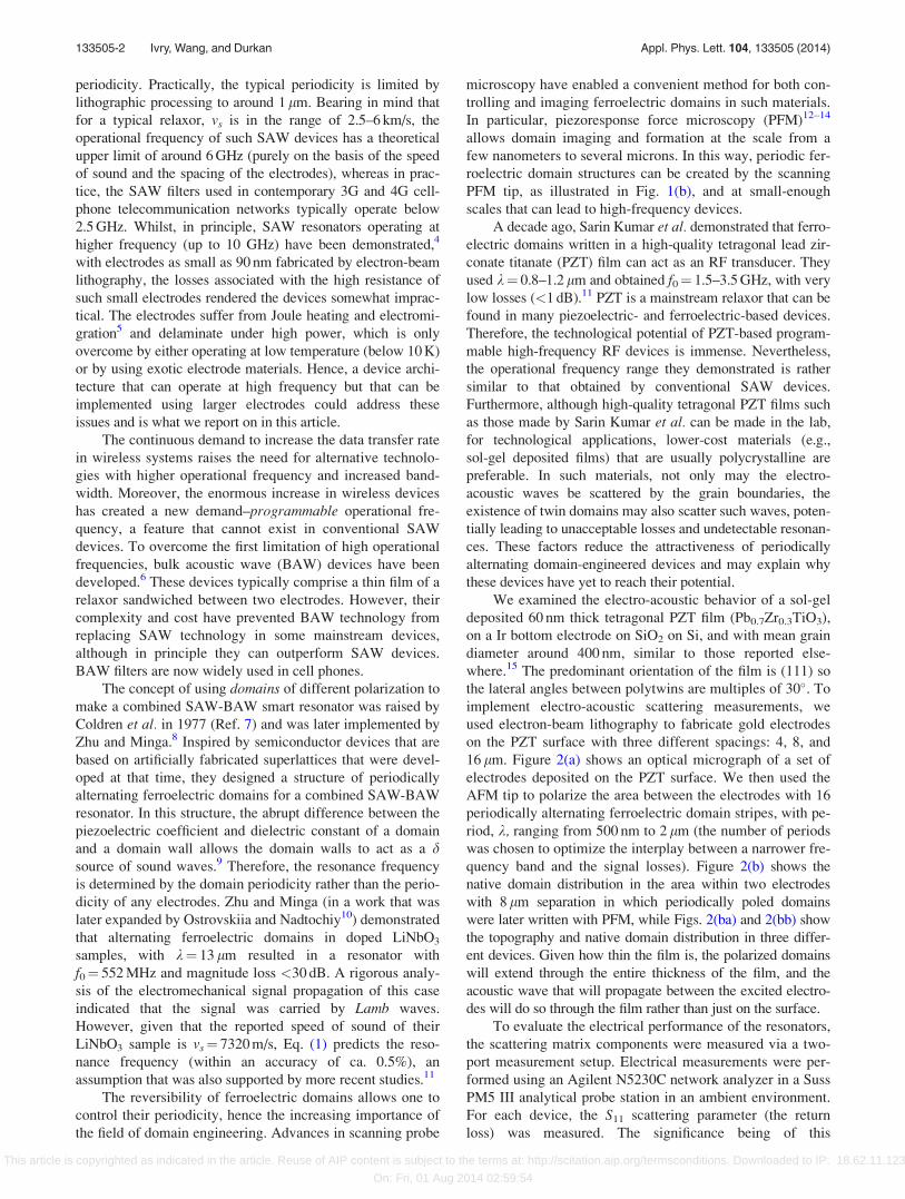
FIG. 2. (a) Optical micrographs of electrodes with 16 lm, 8 lm, and 4 lm
gaps, respectively. (b): (a) Topography and polarization distribution in the
area between the 8 lm separated electrodes; (b) PFM magnitude imaging
before; and (c) PFM phase imaging after domain engineering; (d) and (e) the
polarization distributions in the 16 lm and 4 lm devices, respectively, as
observed with the PFM phase signals. The scale bars in (c) and (e) are
1.6 lm and 0.8 lm, respectively.
FIG. 3. S11 scattering measurements for devices with (a) 16 lm, (b) 8 lm,
and (c) 4 lm gap between the metallic electrodes demonstrating a program-
mable f0 of (a) 1.63, (b) 3.66, and (c) 8.8 GHz.
133505-3 Ivry, Wang, and Durkan Appl. Phys. Lett. 104, 133505 (2014)
This article is copyrighted as indicated in the article. Reuse of AIP content is subject to the terms at: http://scitation.aip.org/termsconditions. Downloaded to IP: 18.62.11.123
On: Fri, 01 Aug 2014 02:59:54

Given that there are an equal number of ferroelectric
domains (16) between each pair of electrodes, then we can
conclude that the losses associated with ferroelectric domain
wall motion are small compared to other mechanisms, the
dominant ones being ferroelastic domain wall motion and
scattering from grain boundaries. The domain configurations
we encountered in our devices are far more complex than
those considered by Arlt, and are not homogeneous, so their
model is not straightforward to apply. However, the Debye-
like loss characteristics suggest a relaxation frequency in the
GHz range for a pure ferroelectric film, and the presence of
elastic or electric stress fields will increase this frequency.
We therefore suggest that the internal elastic fields associ-
ated with the multitude of ferroelastic domain walls within
our material serve to greatly increase the relaxation fre-
quency, enough that we are able to observe filter like charac-
teristics up to almost 9 GHz.
Another point to note is that our device configuration
only involves one set of two electrodes as opposed to two
sets of >�15 as is found in a typical SAW device, and ulti-
mately, the domains could be engineered using a conductive
contact stamp rather than an AFM tip, so massively parallel
fabrication is a possibility, and one could simply re-stamp
with different domain periodicity without needing to fabri-
cate an entirely new device.
In summary, we have demonstrated a simple SAW filter
configuration where the resonator comprises engineered fer-
roelectric nano-domains. We have shown that a polycrystal-
line thin film is capable of transmitting SAW waves beyond
8 GHz.
1P. Luginbuhl, N. F. de Rooij, S. D. Collins, G.-A. Racine, N. J. Setter, and
K. G. Brooks, Proc. SPIE 2978, 129 (1997).2A. O. Marino and R. O. Becker, Nature 228, 473 (1970).3J. W. S. Rayleigh, Proc. London Math. Soc. 17, 4 (1885).4K. Yamanouchi, Hideyuki Nakagawa, J. A. Qureshi, and H. Odagawa,
Jpn. J. Appl. Phys., Part 1 38, 3270 (1999).5F. Hadeed and C. Durkan, Appl. Phys. Lett. 91, 123120 (2007).6Y. Satoh, T. Nishihara, T. Yokoyama, M. Ueda, and T. Miyashita, Jpn. J.
Appl. Phys., Part 1 44, 2883 (2005).7B. A. Coldren, A. M. Glass, and R. A. Lemons, “Acoustic wave device,”
U.S. patent 4,117,424 (30 March 1977).8Y.-Y. Zhu and N.-B. Minga, J. Appl. Phys. 72, 904 (1992).9H. E. B€ommel and K. Dransfeld, Phys. Rev. 117, 1245 (1960).
10I. V. Ostrovskiia and A. B. Nadtochiy, Appl. Phys. Lett. 86, 222902
(2005).11A. K. Sarin Kumar, P. Paruch, J.-M. Triscone, W. Daniau, S. Ballandras,
L. Pellegrino, D. Marr�e, and T. Tybell, Appl. Phys. Lett. 85, 1757 (2004).12P. Guthner and K. Dransfeld, Appl. Phys. Lett. 61, 1137 (1992).13S. V. Kalinin and D. A. Bonnell, Phys. Rev. B 65, 125408 (2002).14C. Durkan, D. P. Chu, P. Migliorato, and M. E. Welland, Appl. Phys. Lett.
76, 366 (2000).15Y. Ivry, D. P. Chu, and C. Durkan, Appl. Phys. Lett. 94, 162903 (2009).16G. Arlt, U. B€ottinger, and S. Witte, Ann. Phys. 506, 578 (1994).
FIG. 4. (a) Linear relationship between the dominant resonant frequency
and the inverse periodicity of the engineered domains. The straight line is
the linear fit to Eq. (1) suggesting vs¼ 4.2 km/s (standard errors are
0.25 km/s and R2¼ 0.975). (b) Relationship between the reflection loss of
the leading resonance and the device size illustrating the decrease in reflec-
tion losses (which is interpreted as an increase in transmission losses) with
increasing device size.
133505-4 Ivry, Wang, and Durkan Appl. Phys. Lett. 104, 133505 (2014)
This article is copyrighted as indicated in the article. Reuse of AIP content is subject to the terms at: http://scitation.aip.org/termsconditions. Downloaded to IP: 18.62.11.123
On: Fri, 01 Aug 2014 02:59:54