
Faculty of Engineering Chulalongkorn University...
22
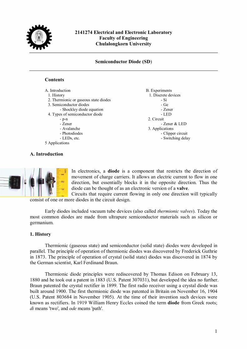
1 2141274 Electrical and Electronic Laboratory Faculty of Engineering Chulalongkorn University Semiconductor Diode (SD) Contents A. Introduction 1. History 2. Thermionic or gaseous state diodes 3. Semiconductor diodes - Shockley diode equation 4. Types of semiconductor diode - p-n - Zener - Avalanche - Photodiodes - LEDs, etc. 5 Applications B. Experiments 1. Discrete devices - Si - Ge - Zener - LED 2. Circuit - Zener & LED 3. Applications - Clipper circuit - Switching delay A. Introduction In electronics, a diode is a component that restricts the direction of movement of charge carriers. It allows an electric current to flow in one direction, but essentially blocks it in the opposite direction. Thus the diode can be thought of as an electronic version of a valve. Circuits that require current flowing in only one direction will typically consist of one or more diodes in the circuit design. Early diodes included vacuum tube devices (also called thermionic valves). Today the most common diodes are made from ultrapure semiconductor materials such as silicon or germanium. 1. History Thermionic (gaseous state) and semiconductor (solid state) diodes were developed in parallel. The principle of operation of thermionic diodes was discovered by Frederick Guthrie in 1873. The principle of operation of crystal (solid state) diodes was discovered in 1874 by the German scientist, Karl Ferdinand Braun. Thermionic diode principles were rediscovered by Thomas Edison on February 13, 1880 and he took out a patent in 1883 (U.S. Patent 307031), but developed the idea no further. Braun patented the crystal rectifier in 1899. The first radio receiver using a crystal diode was built around 1900. The first thermionic diode was patented in Britain on November 16, 1904 (U.S. Patent 803684 in November 1905). At the time of their invention such devices were known as rectifiers. In 1919 William Henry Eccles coined the term diode from Greek roots; di means 'two', and ode means 'path'.
Transcript of Faculty of Engineering Chulalongkorn University...
1
2141274 Electrical and Electronic Laboratory Faculty of Engineering
Chulalongkorn University
Semiconductor Diode (SD)
Contents
A. Introduction 1. History 2. Thermionic or gaseous state diodes 3. Semiconductor diodes
- Shockley diode equation 4. Types of semiconductor diode
- p-n - Zener - Avalanche - Photodiodes - LEDs, etc.
5 Applications
B. Experiments 1. Discrete devices
- Si - Ge - Zener - LED
2. Circuit - Zener & LED
3. Applications - Clipper circuit - Switching delay
A. Introduction
In electronics, a diode is a component that restricts the direction of movement of charge carriers. It allows an electric current to flow in one direction, but essentially blocks it in the opposite direction. Thus the diode can be thought of as an electronic version of a valve. Circuits that require current flowing in only one direction will typically
consist of one or more diodes in the circuit design.
Early diodes included vacuum tube devices (also called thermionic valves). Today the most common diodes are made from ultrapure semiconductor materials such as silicon or germanium.
1. History
Thermionic (gaseous state) and semiconductor (solid state) diodes were developed in parallel. The principle of operation of thermionic diodes was discovered by Frederick Guthrie in 1873. The principle of operation of crystal (solid state) diodes was discovered in 1874 by the German scientist, Karl Ferdinand Braun.
Thermionic diode principles were rediscovered by Thomas Edison on February 13, 1880 and he took out a patent in 1883 (U.S. Patent 307031), but developed the idea no further. Braun patented the crystal rectifier in 1899. The first radio receiver using a crystal diode was built around 1900. The first thermionic diode was patented in Britain on November 16, 1904 (U.S. Patent 803684 in November 1905). At the time of their invention such devices were known as rectifiers. In 1919 William Henry Eccles coined the term diode from Greek roots; di means 'two', and ode means 'path'.

2
2. Thermionic or gaseous state diodes
Thermionic diodes are vacuum tube devices (also known as thermionic valves), which are arrangements of electrodes surrounded by a vacuum within a glass envelope, similar in appearance to incandescent light bulbs. In vacuum tube diodes, a current is passed through the cathode, a filament treated with a mixture of barium and strontium oxides, which are oxides of alkaline earth metals. The current heats the filament, causing thermionic emission of electrons into the vacuum envelope. In forward operation, a surrounding metal electrode, called the anode, is positively charged, so that it electrostatically attracts the emitted electrons. However, electrons are not easily released from the unheated anode surface when the voltage polarity is reversed and hence any reverse flow is a very tiny current. For much of the 20th century vacuum tube diodes were used in analog signal applications, and as rectifiers in power supplies. Today, tube diodes are only used in niche applications, such as rectifiers in tube guitar and hi-fi amplifiers, and specialized high-voltage equipment.
3. Semiconductor diodes
Most modern diodes are based on semiconductor p-n junctions. In a p-n diode, conventional current can flow from the p-type side (the anode) to the n-type side (the cathode), but not in the opposite direction (strictly speaking, this is not true since small reverse current can flow from n to p). A semiconductor diode's current-voltage, or I-V, characteristic curve is ascribed to the behavior
of the so-called depletion layer or depletion zone which exists at the p-n junction. When a p-n junction is formed, mobile electrons from the negatively, n-doped region diffuse into the positively, p-doped region where there is a large population of holes and "recombine". When a mobile electron recombines with a hole, the hole vanishes and the electron is no longer mobile. Thus, two charge carriers have vanished. The region around the p-n junction becomes depleted of charge carriers and thus behaves as an insulator. However, the depletion width cannot grow without limit. For each electron-hole pair that recombines, a positively-charged dopant ion is left behind in the N-doped region, and a negatively-charged dopant ion is left behind in the P-doped region. As recombination proceeds and more ions are created, an increasing electric field develops through the depletion zone which acts to slow and then finally stop recombination. At this point, there is a 'built-in' potential across the depletion zone. If an external voltage is placed across the diode with the same polarity as the built-in potential, the depletion zone continues to act as an insulator preventing a significant electric current. However, if the polarity of the external voltage opposes the built-in potential, recombination can once again proceed resulting in substantial electric current through the p-n junction. For silicon diodes, the built-in potential is approximately 0.6 V. Thus, if an external current is passed through the diode, about 0.6 V will be developed across the diode such that the P-doped region is positive with respect to the N-doped region and the diode is said to be 'turned on'.
A diode's I-V characteristic can be approximated by two regions of operation. Below a certain difference in potential between the two leads, the depletion layer has significant width, and the diode can be thought of as an open (non-conductive) circuit. As the potential difference is increased, at some stage the diode will become conductive and allow charges to flow, at which point it can be thought of as a connection with zero (or at least very low) resistance. More precisely, the transfer function is logarithmic, which means that it looks like
Cathode
Anode
3
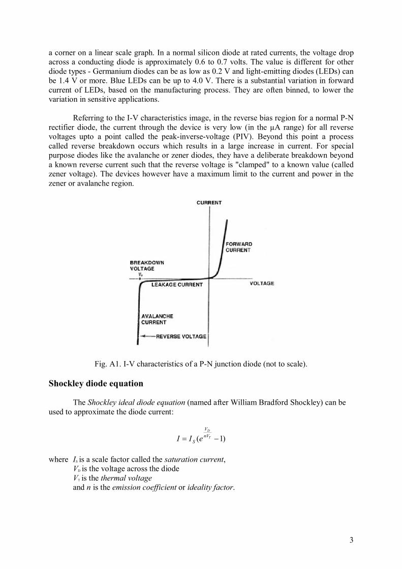
a corner on a linear scale graph. In a normal silicon diode at rated currents, the voltage drop across a conducting diode is approximately 0.6 to 0.7 volts. The value is different for other diode types - Germanium diodes can be as low as 0.2 V and light-emitting diodes (LEDs) can be 1.4 V or more. Blue LEDs can be up to 4.0 V. There is a substantial variation in forward current of LEDs, based on the manufacturing process. They are often binned, to lower the variation in sensitive applications.
Referring to the I-V characteristics image, in the reverse bias region for a normal P-N
rectifier diode, the current through the device is very low (in the µA range) for all reverse voltages upto a point called the peak-inverse-voltage (PIV). Beyond this point a process called reverse breakdown occurs which results in a large increase in current. For special purpose diodes like the avalanche or zener diodes, they have a deliberate breakdown beyond a known reverse current such that the reverse voltage is "clamped" to a known value (called zener voltage). The devices however have a maximum limit to the current and power in the zener or avalanche region.
Fig. A1. I-V characteristics of a P-N junction diode (not to scale).
Shockley diode equation
The Shockley ideal diode equation (named after William Bradford Shockley) can be used to approximate the diode current:
)1( T
D
nV
V
S eII
where IS is a scale factor called the saturation current,
VD is the voltage across the diode VT is the thermal voltage and n is the emission coefficient or ideality factor.

4
The ideality factor n varies from about 1 to 2 depending on the fabrication process and semiconductor material and in many cases is assumed to be approximately equal to 1 (thus omitted). The thermal voltage VT is approximately 26 mV at room temperature (approximately 25oC or 298K) and is a known constant. It is defined by:
q
kTVT
where q is the charge on an electron (the elementary charge),
k is Boltzmann's constant, T is the absolute temperature of the p-n junction.
4. Types of semiconductor diode
Diode Light-EmittingDiode
ZenerDiode
SchottkyDiode
Fig. A2. Some diode symbols
There are several types of semiconductor diodes: (* denotes the types of diodes to be investigated in this lab session) *Normal (p-n) diodes
which operate as described above. Usually made of doped silicon or, more rarely, germanium.
*Zener diodes Diodes that can be made to conduct backwards. This effect, called Zener breakdown, occurs at a precisely defined voltage, allowing the diode to be used as a precision voltage reference. In practical voltage reference circuits Zener and switching diodes are connected in series and opposite directions to balance the temperature coefficient to near zero. Some devices labeled as high-voltage Zener diodes are actually avalanche diodes.
Avalanche diodes
diodes that conduct in the reverse direction when the reverse bias voltage exceeds the breakdown voltage. These are electrically very similar to Zener diodes, and are often mistakenly called Zener diodes, but break down by a different mechanism, the avalanche effect. This occurs when the reverse electric field across the p-n junction causes a wave of ionization, reminiscent of an avalanche, leading to a large current. Avalanche diodes are designed to break down at a well-defined reverse voltage without being destroyed. The difference between the avalanche diode (which has a reverse breakdown above about 6.2 V) and the Zener is that the channel length of the former exceeds the 'mean free path' of the electrons, so there are collisions between
5
them on the way out. The only practical difference is that the two types have temperature coefficients of opposite polarities.
Photodiodes Semiconductors are subject to optical charge carrier generation and therefore most are packaged in light blocking material. If they are packaged in materials that allow light to pass, their photosensitivity can be utilized. Photodiodes can be used as solar cells, and in photometry.
*Light-emitting diodes (LEDs) In a diode formed from a direct band-gap semiconductor, such as gallium arsenide, carriers that cross the junction emit photons when they recombine with the majority carrier on the other side. Depending on the material, wavelengths (or colors) from the infrared to the near ultraviolet may be produced. The forward potential of these diodes is indicative of the wavelength of the emitted photons: 1.2 V corresponds to red, 2.4 to violet. The first LEDs were red and yellow, and higher-frequency diodes have been developed over time. All LEDs are monochromatic; 'white' LEDs are actually combinations of three LEDs of a different color, or a blue LED with a yellow scintillator coating. LEDs can also be used as low-efficiency photodiodes in signal applications. An LED may be paired with a photodiode or phototransistor in the same package, to form an opto-isolator or opto-coupler.
Laser diodes When an LED-like structure is contained in a resonant cavity formed by polishing the parallel end faces, a laser can be formed. Laser diodes are commonly used in optical storage devices and for high speed optical communication.
Schottky diodes have a lower forward voltage drop than a normal PN junction, because they are constructed from a metal to semiconductor contact. Their forward voltage drop at forward currents of about 1 mA is in the range 0.15 V to 0.45 V, which makes them useful in voltage clamping applications and prevention of transistor saturation. They can also be used as low loss rectifiers although their reverse leakage current is generally much higher than non Schottky rectifiers. Schottky diodes are majority carrier devices and so do not suffer from minority carrier storage problems that slow down most normal diodes. They also tend to have much lower junction capacitance than PN diodes and this contributes towards their high switching speed and their suitability in high speed circuits and RF devices such as mixers and detectors.
PIN diodes
A PIN diode has a central un-doped, or intrinsic, layer, forming a p-type / intrinsic / n-type structure. They are used as radio frequency switches, similar to varactor diodes but with a more sudden change in capacitance. They are also used as large volume ionizing radiation detectors and as photodetectors. PIN diodes are also used in power electronics, as their central layer can withstand high voltages. Furthermore, the PIN structure can be found in many power semiconductor devices, such as IGBTs, power MOSFETs, and thyristors.

6
5. Applications Radio demodulation
The first use for the diode was the demodulation of amplitude modulated (AM) radio broadcasts. In summary, an AM signal consists of alternating positive and negative peaks of voltage, whose amplitude or 'envelope' is proportional to the original audio signal, but whose average value is zero. The diode rectifies the AM signal, leaving a signal whose average amplitude is the desired audio signal. The average value is extracted using a simple filter and fed into an audio transducer, which generates sound.
Power conversion Rectifiers are constructed from diodes, where they are used to convert alternating current (AC) electricity into direct current (DC).
Over-voltage protection
Diodes are frequently used to conduct damaging high voltages away from sensitive electronic devices. They are usually reverse-biased (non-conducting) under normal circumstances, and become conducting when the voltage rises above their peakinversion voltages (PIVs). For example, diodes are used in stepper motor and relay circuits to de-energize coils rapidly without the damaging voltage spikes that would otherwise occur. Many integrated circuits also incorporate diodes on the connection pins to prevent external voltages from damaging their sensitive transistors. Specialized diodes are used to protect from over-voltages at higher power (see Diode types above).
Logic gates
Diodes can be combined with other components to construct AND and OR logic gates.
Temperature sensors
A diode can be used as a temperature measuring device, since the forward voltage drop across the diode depends on temperature. This temperature dependence follows from the Shockley ideal diode equation given above.
Charge coupled devices
Digital cameras and similar units use arrays of photo diodes, integrated with readout circuitry.
7
B. Experiments
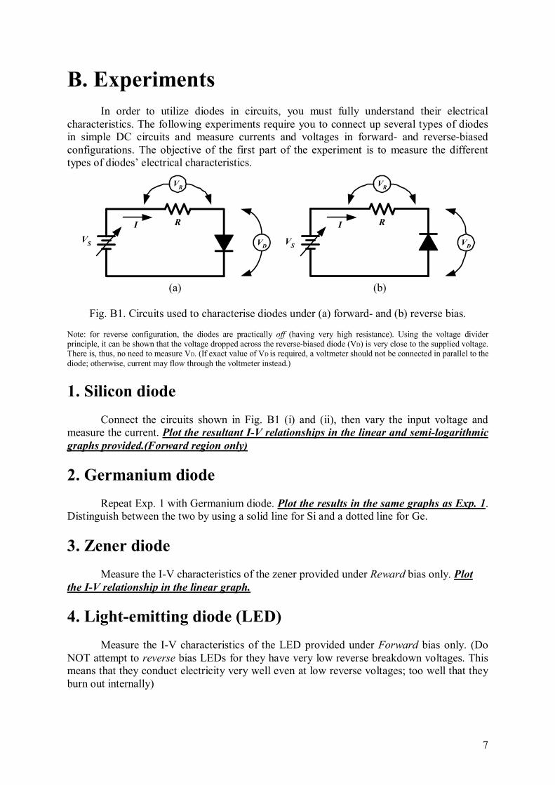
In order to utilize diodes in circuits, you must fully understand their electrical characteristics. The following experiments require you to connect up several types of diodes in simple DC circuits and measure currents and voltages in forward- and reverse-biased configurations. The objective of the first part of the experiment is to measure the different types of diodes’ electrical characteristics.
VD
RI
VR
VS VD
RI
VR
VS
(a) (b)
Fig. B1. Circuits used to characterise diodes under (a) forward- and (b) reverse bias.
Note: for reverse configuration, the diodes are practically off (having very high resistance). Using the voltage divider principle, it can be shown that the voltage dropped across the reverse-biased diode (VD) is very close to the supplied voltage. There is, thus, no need to measure VD. (If exact value of VD is required, a voltmeter should not be connected in parallel to the diode; otherwise, current may flow through the voltmeter instead.)
1. Silicon diode
Connect the circuits shown in Fig. B1 (i) and (ii), then vary the input voltage and measure the current. Plot the resultant I-V relationships in the linear and semi-logarithmic graphs provided.(Forward region only)
2. Germanium diode
Repeat Exp. 1 with Germanium diode. Plot the results in the same graphs as Exp. 1. Distinguish between the two by using a solid line for Si and a dotted line for Ge.
3. Zener diode
Measure the I-V characteristics of the zener provided under Reward bias only. Plot the I-V relationship in the linear graph.
4. Light-emitting diode (LED)
Measure the I-V characteristics of the LED provided under Forward bias only. (Do NOT attempt to reverse bias LEDs for they have very low reverse breakdown voltages. This means that they conduct electricity very well even at low reverse voltages; too well that they burn out internally)

8
Having completed characterizing the diodes on their own, you are ready to combine them in a circuit and learn how they work together. The following experiment does not have practical applications but it serves to increase your analytical skills.
5. Zener and LED circuit
Connect the circuit shown in Fig. B2 and increase the voltage supply such that you
can see some light coming out of the LED. Measure the values required in the table. Then increase the voltage supply further to get strong light coming out of the LED and re-measure the values (keep current well below 30mA).
mA
470
0-12 V
Fig. B2.
Now, for some useful applications. In Section A, it was briefly mentioned that diodes
can be useful in power conversion (AC to DC) and logic gates. In the following experiments, you will see how the diode characteristic can be used to process a signal (Exp. 6). You will also measure a diode’s storage delay time which is a limiting factor in switching or logic applications (Exp. 7).
6. Clipper circuit
Connect the circuit shown in Fig. B3 using Si diodes. The input and output voltages are to be observed via CH1 and CH2 of the CRO, respectively. The input voltage (Vi) is a sinusoidal signal with a frequency of 1 kHz. Start the experiment with a small amplitude (e.g. 0.1 V peak)
1k
VoViD1 D2
Fig. B3.
6.1. Vary the amplitude of Vi and record the voltage waveforms at the input (CH1) and output (CH2) when the peak value of Vi is set to 0.1V and 1V.

9
(Before proceeding, set the amplitude of Vi to 1V peak and make sure that the CRO is triggered by CH1. This is to make sure that the input waveform, CH1, in the following two mini-experiments stay the same)
6.2. Disconnect diode D1 and record the output waveform (CH2).
6.3. Put diode D1 back in (be careful with the polarity). Then, disconnect diode D2 and record the output waveform (CH2) in the same graph as Exp. 6.2.
7. Switching Delay
Ideal diodes do not allow current to flow under reverse bias conditions. Real diodes however, momentarily allow current to flow under reverse bias conditions. This is due to the fact that diodes under forward bias store significant amount of charge across the depletion width and these charge carriers must be removed under reverse bias. The removal mechanism is called recombination, and it takes time. The time taken to remove the stored charge is termed the storage delay time (tsd). In the following, you will measure tsd of a Si diode.
Vi
i
RL VR6V
50kHz
Fig. B4.
7.1 Connect the circuit shown in Fig. B4 using a Si diode. The input is a square wave
with a frequency of 50 kHz and an amplitude of 6V peak-to-peak. The load resistance (RL) is 1 k.. Plot Vi and VR in the same graph. Also show VR-ideal on the same graph if the diode were ideal (this is for comparison purposes). Expand the time axis until only a few complete cycles fill the CRO screen. Now, you can determine tr by measuring the duration between the point when the diode should be off (the falling edge of Vi) and the point when it is off. What is the tr of the Si diode? (The reverse recovery time tr, consists of the storage delay time tsd and the decay time td.)
7.2 Increase the amplitude of Vi to 8 and 10 V peak-to-peak and plot VR in the same
graph.
7.3 Return Vi to 6V peak-to-peak and frequency of 50 kHz, compare the switching behavior between Si and Ge diode.
In summary, you have measured the electrical (I-V) characteristics of Si, Ge, Ze, and light-emitting diodes. You have also constructed simple diode circuits that perform clipping and switching functions.

10

11
Student Name: ID: Date: Group: Instructor signature:
Experimental Report
Cathode-Ray Oscilloscope (CRO)
Exp1 & 2 Si and Ge diodes
Si diode Forward bias
I () 6 10 30 60 100 300 600 1,000 3,000
VR (Volt)
VD (Volt)
Reverse bias
VD (Volt) 5 10
VR (Volt)
I ()
Ge diode
Forward bias
I () 6 10 30 60 100 300 600 1,000 3,000
VR (Volt)
VD (Volt)
Reverse bias
VD (Volt) 5 10 15 20
VR (Volt)
I (A)

12
Linear I-V plot (forward bias): Si & Ge diode

13
Semi-Logarithmic I-V plot (forward bias): Si & Ge diode

14
Discussion

15
Exp 3 Zener diode (Reverse bias only)
I () 6 10 30 60 100 300 600 1,000 3,000
VR (Volt)
VD (Volt)
Discussion

16
Linear I-V plot: Zener diode
17
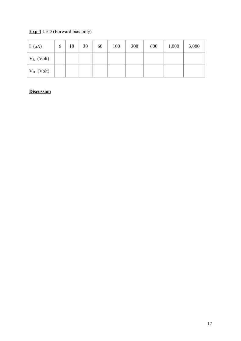
Exp 4 LED (Forward bias only)
I () 6 10 30 60 100 300 600 1,000 3,000
VR (Volt)
VD (Volt)
Discussion

18
Linear I-V plot (forward bias only): LED
19
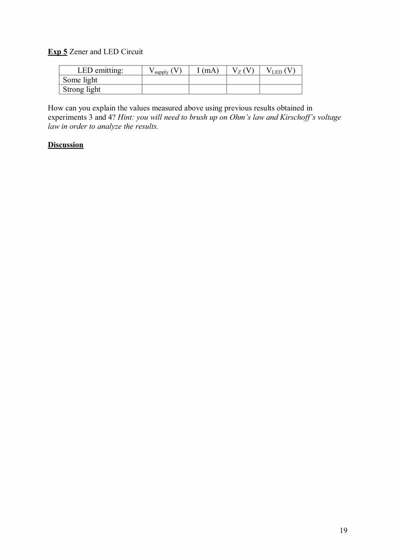
Exp 5 Zener and LED Circuit
LED emitting: Vsupply (V) I (mA) VZ (V) VLED (V) Some light Strong light
How can you explain the values measured above using previous results obtained in experiments 3 and 4? Hint: you will need to brush up on Ohm’s law and Kirschoff’s voltage law in order to analyze the results. Discussion

20
Exp 6 Clipper circuit 6.1
Vi-peak = 0.1 V Vi-peak = 1 V
Is there a relation ship between the above results and those obtained in Exp 1? 6.2 & 6.3
Discussion

21
Exp 7 Switching Delay 7.1 Si diode with input frequency = 50 kHz
tsd = 7.2 Si diode with various amplitude
7.3 Compare the switching characteristics between Si and Ge diode
Si diode Ge diode

22
Discussion