Three Year Visual and Endothelial Density Outcomes after Endothelial Keratoplasty
1
2012 Master thesis
Evaluation of interface state density in
three-dimensional SiO2 gated MOS capacitors
Supervisor
Professor Hiroshi Iwai
Department of Electronics and Applied Physics
Interdisciplinary Graduate School of Science and
Engineering
Tokyo Institute of Technology
10M53567
Wei Li
2
CONTENTS
Chapter 1 Introduction 1.1 CMOS Scaling 5 1.2 Planar Device Scaling Limit 6 1.3 Introduction of Three-Dimensional Structure 9 1.4 Purpose of This Thesis 13 References 14
Chapter 2 Fabrication and Characterization Method 2.1 Substrate Cleaning 17 2.2 Thermal Oxidation Process 17 2.3 Photolithograph 19 2.4 RF Magnetron Sputtering 22 2.5 Thermal Evaporation for Al Back Contact 23 2.6 Rapid Thermal Annealing Process 24 2.7 Capacitance-Voltage (C-V) Curves 25 2.8 Conductance Method 29 2.9 Quasi-static Method 32 2.10 Scanning Electron Microscopy (SEM) Method 34 2.11 Conclusion of This Chapter 36 References 37
3
Chapter 3 Interface State Density Extraction of Three-Dimensional Channel Structure 3.1 Device Fabrication Process 39 3.2 Analysis of Fin Structure with SEM Images 41 3.3 Analysis of C-V Curves 43 3.4 Extraction of Interface State Density of planar and Fin devices by Quasi-static C-V Method 44 3.5 Extraction of Interface State Density of planar devices by Conductance Method 47 3.6 Conclusion of This Chapter 50 References 51
Chapter 4 Modeling of Conductance Spectra by Deconvolution 4.1 Numerical simulation of surface potential of 3D channel 53 4.2 Deconvolution of Conductance Spectra of Fin Devices 54 4.3 Conclusion of This Chapter 55 References 56
Chapter 5 Conclusion of This Study 5.1 Conclusion 57 Acknowledgments
4
Chapter1 Introduction
1.1 CMOS Scaling
1.2 Planar Device Scaling Limit
1.3 Introduction of Three-Dimensional Structure
1.4 Issues of Three-Dimensional Structure
1.5 Purpose of This Thesis
References
5
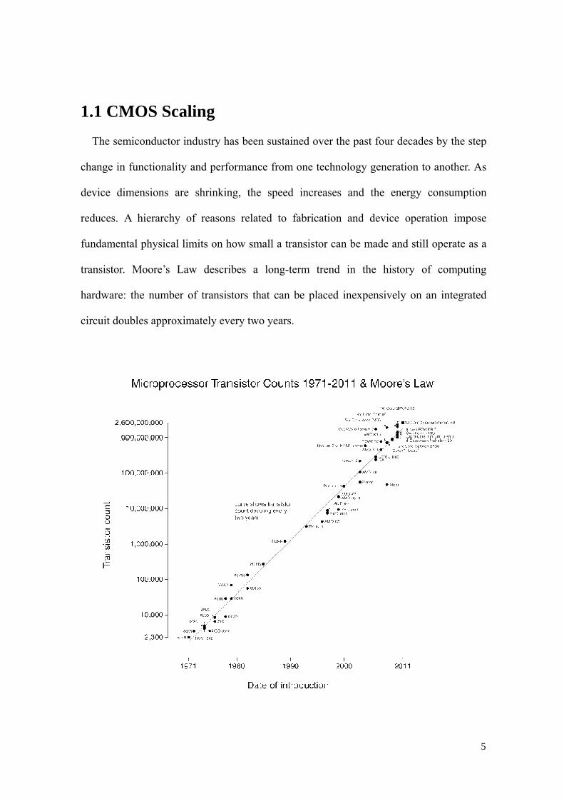
1.1 CMOS Scaling The semiconductor industry has been sustained over the past four decades by the step
change in functionality and performance from one technology generation to another. As
device dimensions are shrinking, the speed increases and the energy consumption
reduces. A hierarchy of reasons related to fabrication and device operation impose
fundamental physical limits on how small a transistor can be made and still operate as a
transistor. Moore’s Law describes a long-term trend in the history of computing
hardware: the number of transistors that can be placed inexpensively on an integrated
circuit doubles approximately every two years.
6
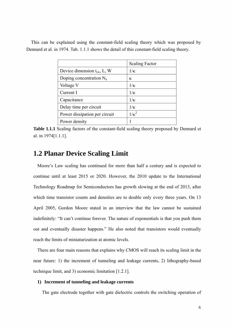
This can be explained using the constant-field scaling theory which was proposed by Dennard et al. in 1974. Tab. 1.1.1 shows the detail of this constant-field scaling theory.
Scaling Factor Device dimension tox, L, W 1/κ Doping concentration Na κ Voltage V 1/κ Current I 1/κ Capacitance 1/κ Delay time per circuit 1/κ Power dissipation per circuit 1/κ2 Power density 1
Table 1.1.1 Scaling factors of the constant-field scaling theory proposed by Dennard et al. in 1974[1.1.1].
1.2 Planar Device Scaling Limit
Moore’s Law scaling has continued for more than half a century and is expected to
continue until at least 2015 or 2020. However, the 2010 update to the International
Technology Roadmap for Semiconductors has growth slowing at the end of 2013, after
which time transistor counts and densities are to double only every three years. On 13
April 2005, Gordon Moore stated in an interview that the law cannot be sustained
indefinitely: “It can’t continue forever. The nature of exponentials is that you push them
out and eventually disaster happens.” He also noted that transistors would eventually
reach the limits of miniaturization at atomic levels.
There are four main reasons that explains why CMOS will reach its scaling limit in the
near future: 1) the increment of tunneling and leakage currents, 2) lithography-based
technique limit, and 3) economic limitation [1.2.1].
1) Increment of tunneling and leakage currents
The gate electrode together with gate dielectric controls the switching operation of
7
CMOS transistors. The voltage of the gate electrode controls the flow of electric
current across the transistor. The gate dielectric should be made as thin as possible to
increase the performance of the transistor. In additional, it is critical to keep short
channel effects under control when a transistor is turned on and reduce sub-threshold
leakage when a transistor is off. In order to maintain the electric field as CMOS
transistors are scaled, the gate dielectric thickness should also be shrunk proportionally.
An oxide thickness of 3 nm is needed for CMOS transistors with channel lengths of
100 nm or less [1.2.2]. This thickness comprises only a few layers of atoms and is
approaching fundamental limits which is around 1 to 1.5 nm[1.2.3]. The thin oxide
layer is subject to quantum-mechanical tunneling, giving rise to a gate leakage current
that increases exponentially as the oxide thickness is scaled down. This tunneling
current can initiate a damage leading to the fallible of the dielectric.
2) Lithography-based technique limit
CMOS transistors are basically patterned on wafer by means of lithography and
masks. It means that the lithography technology is one of the main drives behind the
transistor scaling. Ironically, the lithography processes cannot cope with the shrinking
feature of CMOS transistors' layout. Lithography techniques such as proximity X-ray
steppers and ion beam are limited by difficulties in controlling mask-wafer gap and
uniform exposure of photoresists on wafer respectively. Another problem is the
inability of polishing process to maintain the uniform thickness of wafer and reliable
mask. According to [1.2.4], patterning smaller feature than wavelength of light
requires trade-off between complex, costly masks and possible design constraint. So
the current optical-based fabrication technology may be not able to support the
resolution that is needed to pattern feature smaller CMOS sizes.
8
3) Economic limitation
Another biggest drive behind the downscaling is the economic consideration. The
rising cost in semiconductor sector is basically contributed by the cost of production,
and testing that escalating exponentially with time as the CMOS size is scaling down.
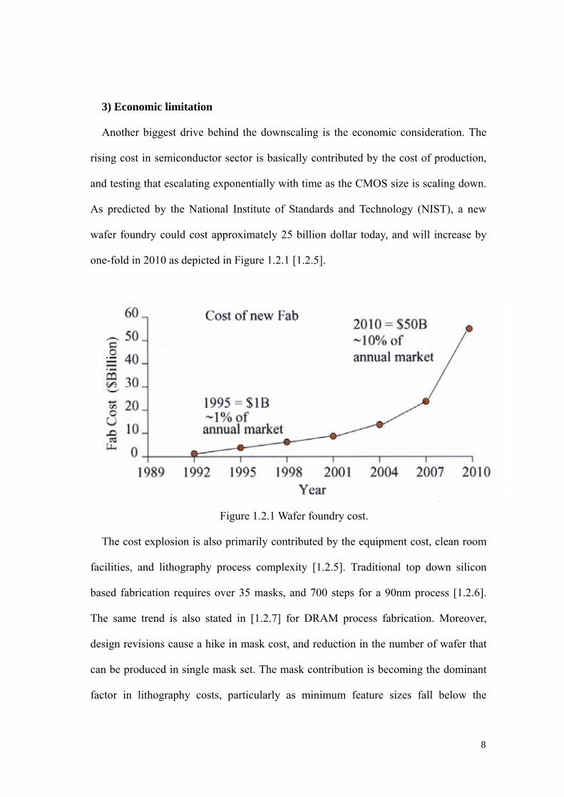
As predicted by the National Institute of Standards and Technology (NIST), a new
wafer foundry could cost approximately 25 billion dollar today, and will increase by
one-fold in 2010 as depicted in Figure 1.2.1 [1.2.5].
Figure 1.2.1 Wafer foundry cost.
The cost explosion is also primarily contributed by the equipment cost, clean room
facilities, and lithography process complexity [1.2.5]. Traditional top down silicon
based fabrication requires over 35 masks, and 700 steps for a 90nm process [1.2.6].
The same trend is also stated in [1.2.7] for DRAM process fabrication. Moreover,
design revisions cause a hike in mask cost, and reduction in the number of wafer that
can be produced in single mask set. The mask contribution is becoming the dominant
factor in lithography costs, particularly as minimum feature sizes fall below the
9
exposure wavelength. These problems lead to the combination of wafer production to
the best equipped foundries [1.2.8]. The alliances between companies and
participation from universities and government that inject funding are also the strategy
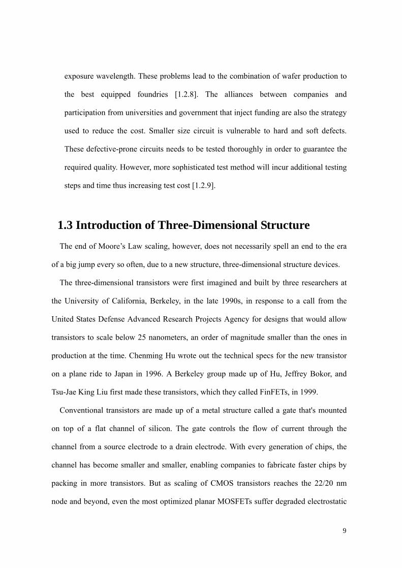
used to reduce the cost. Smaller size circuit is vulnerable to hard and soft defects.
These defective-prone circuits needs to be tested thoroughly in order to guarantee the
required quality. However, more sophisticated test method will incur additional testing
steps and time thus increasing test cost [1.2.9].
1.3 Introduction of Three-Dimensional Structure The end of Moore’s Law scaling, however, does not necessarily spell an end to the era
of a big jump every so often, due to a new structure, three-dimensional structure devices.
The three-dimensional transistors were first imagined and built by three researchers at
the University of California, Berkeley, in the late 1990s, in response to a call from the
United States Defense Advanced Research Projects Agency for designs that would allow
transistors to scale below 25 nanometers, an order of magnitude smaller than the ones in
production at the time. Chenming Hu wrote out the technical specs for the new transistor
on a plane ride to Japan in 1996. A Berkeley group made up of Hu, Jeffrey Bokor, and
Tsu-Jae King Liu first made these transistors, which they called FinFETs, in 1999.
Conventional transistors are made up of a metal structure called a gate that's mounted
on top of a flat channel of silicon. The gate controls the flow of current through the
channel from a source electrode to a drain electrode. With every generation of chips, the
channel has become smaller and smaller, enabling companies to fabricate faster chips by
packing in more transistors. But as scaling of CMOS transistors reaches the 22/20 nm
node and beyond, even the most optimized planar MOSFETs suffer degraded electrostatic
10
behavior. As transistor scaling gets smaller and smaller, conventional transistors are
subject to a problem called leakage. This means that when the transistor is in the "off"
state, a small amount of current still flows through. This leads to errors and drains power.
However, the three-dimensional structure has shown a different performance. Intel's
three-dimensional structure channel is a raised "fin" of silicon surrounded on three sides
by the gate. This allows for a more intimate connection between the gate and the channel,
and that in turn enables better control, greatly reducing leakage.
Since last year, Intel has shown off the design of its next generation of chips. The new
transistor design, which uses a three-dimensional gate rather than a flat one, will go into
production at the company's fabs this year. The company says the three-dimensional
structure will allow the company to double the density of its chips while also providing
performance gains and lower power consumption. It is the first large-volume production of
three-dimensional transistors. The new chips are 37 percent faster than the company's
current ones when operating at low voltages to keep power consumption low. And they
require half the power to perform at a given switching speed. Power consumption is
important in handheld devices because it determines how long the battery lasts. It's also
crucial in the power-hungry server farms that make up the cloud.
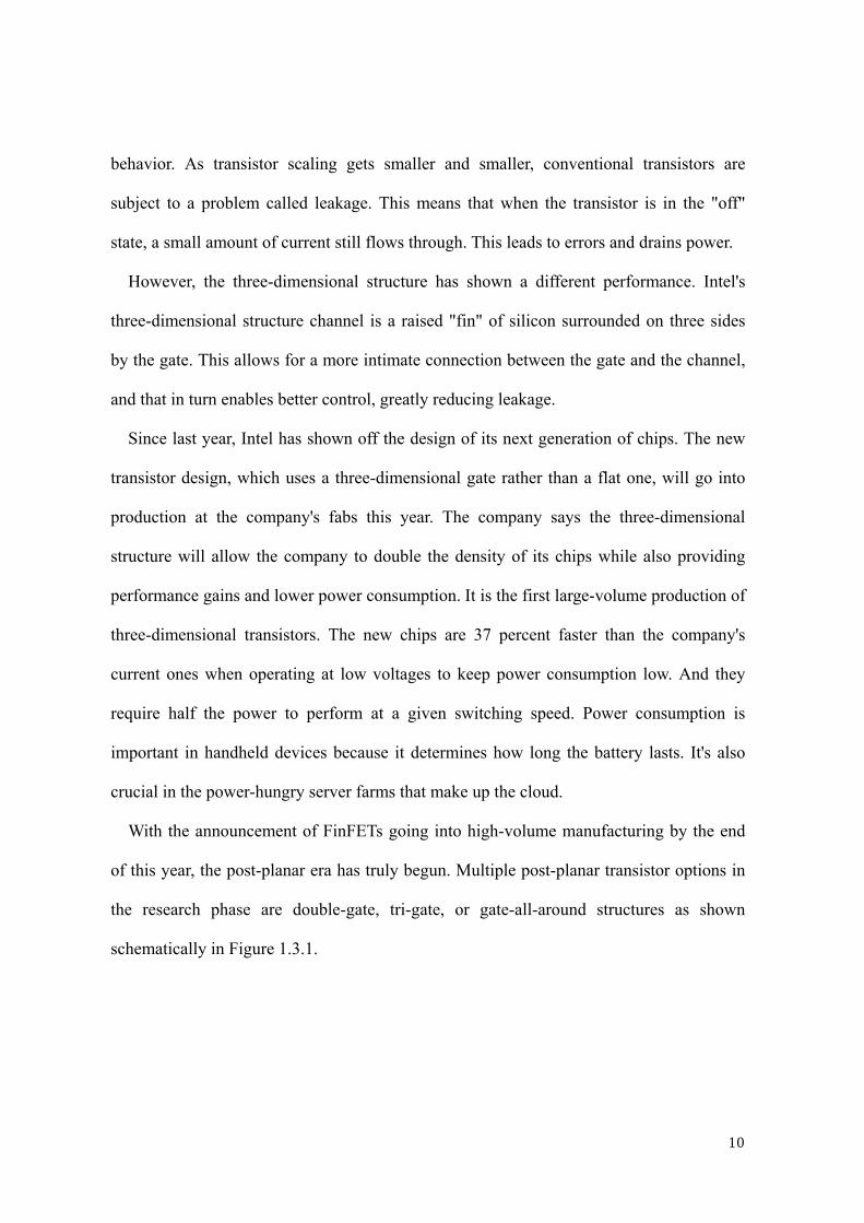
With the announcement of FinFETs going into high-volume manufacturing by the end
of this year, the post-planar era has truly begun. Multiple post-planar transistor options in
the research phase are double-gate, tri-gate, or gate-all-around structures as shown
schematically in Figure 1.3.1.

11
G G
Double-gate
G G
Tri-gate
G
All -around
A. B. C.
Figure 1.3.1 Multiple post-planar transistor options[1.3.3]
Double-gate MOSFET consists of a vertical Si fin controlled by self-aligned
double-gate which is schematically shown in Figure 1.3.1(A). Double-gate MOSFET is
close to the conventional MOSFET in layout and fabrication. The features of
Double-gate MOSFET structure include (1) an ultra-thin Si fin for suppression of
short-channel effects; (2) two gates which are self-aligned to each other; (3) raised the
source/drain to reduce parasitic resistance; (4) a short Si fin for quasi-planar topography;
and (5) gate-last process compatible with low-T, high-k gate dielectrics[1.3.5]
Though double-gate transistors offer excellent short channel effect control, the vertical
nature of the device and the difficulties in fabricating such a device suggest that the
Tri-Gate might be the next transistor design. Tri-Gate structure is shown in Figure
1.3.1(B). It has been reported that the tri-gate devices demonstrated that full depletion at
silicon body dimensions approximately 1.5-2 times greater than either single gate SOI or
double-gate SOI for similar gate lengths, indicating that tri-gate devices are easier to
fabricate using the conventional fabrication tools [1.3.6].
12
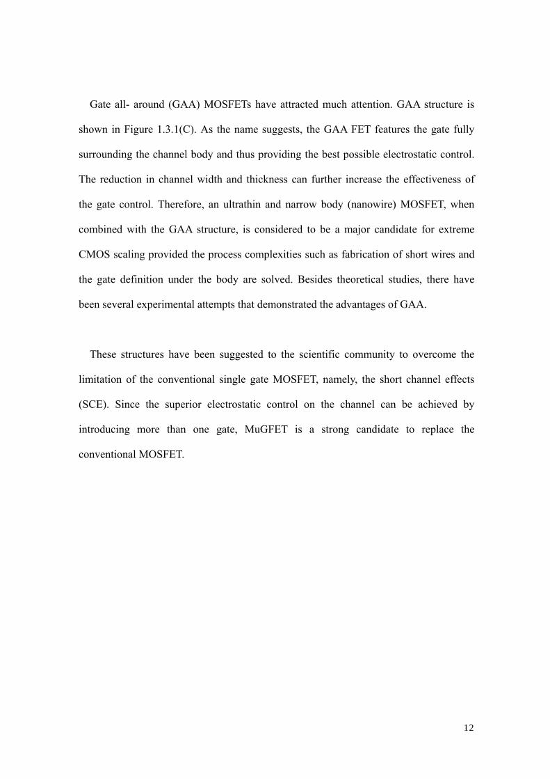
Gate all- around (GAA) MOSFETs have attracted much attention. GAA structure is
shown in Figure 1.3.1(C). As the name suggests, the GAA FET features the gate fully
surrounding the channel body and thus providing the best possible electrostatic control.
The reduction in channel width and thickness can further increase the effectiveness of
the gate control. Therefore, an ultrathin and narrow body (nanowire) MOSFET, when
combined with the GAA structure, is considered to be a major candidate for extreme
CMOS scaling provided the process complexities such as fabrication of short wires and
the gate definition under the body are solved. Besides theoretical studies, there have
been several experimental attempts that demonstrated the advantages of GAA.
These structures have been suggested to the scientific community to overcome the
limitation of the conventional single gate MOSFET, namely, the short channel effects
(SCE). Since the superior electrostatic control on the channel can be achieved by
introducing more than one gate, MuGFET is a strong candidate to replace the
conventional MOSFET.
13
1.4 Purpose of this thesis Silicon metal-oxide-semiconductor (MOS) field-effect-transistors (FETs) with
three-dimensional (3D) channels, such as Fin FETs, Tri-gates and Si nanowire FETs,
have attracted a strong interest owing to their excellent properties [1.5.1]. Performance
and reliability of 3D-channel devices are largely dependent on the electrical properties of
insulator and silicon interfaces. Crystallographic orientation of silicon surface is one of
the main determinants of the interface quality, and commonly (100) surfaces are used to
meet the device performance. As 3D channels consist of several crystallographic
orientations, the interface state density (Dit) of 3D surfaces may become an issue for
device performance.
Two methods have been adopted in this study to obtain characteristics of interface
state density of three-dimensional MOS devices. One is quasi-static capacitance-voltage
method and the other is conductance method. By comparison of the results obtained by
these two methods, an evaluation of interface state density in three-dimensional devices
has been proposed.
14
Refernces
[1.1.1] R. H. Dennard, F. H. Gaensslen, H. N. Yu, V. L. Rideout, E. Bassous, and A.
R.LeBlanc. Design of ion-implanted MOSFETs with very small physical dimensions.
IEEE. J. Solid-State Circuits.
[1.2.1] Harson, N.Z; Hamdioui, S; Design and Test Workshop, 2008.IDT 2008. 3rd
International,pp: 98-103.
[1.2.2] Y. Taur, "CMOS design near the limit of scaling", IBM Journal ofR&D, vol. 46,
iss. 2, pp. 213-222, 2002.
[1.2.3] R. D. Isaac, "The Future of CMOS Technology", IBM Journal ofR&D, vol. 44,
iss. 3, pp. 369-378, 2000.
[1.2.4] T. Skotnicki, et. aI, "The End of CMOS Scaling: Towards the Introduction of
New Materials and Structural Changes to Improve MOSFET Performance", IEEE
Circuits and Devices Magazine, vol. 21, issues 1, pp. 16-26, 2005.
[1.2.5] A. W. Wieder and F. Neppi, "CMOS Technology Trends and Economics", IEEE
Micro, vol. 12 , iss. 4, pp. 10-19, 1992.
[1.2.6] W. Trybula, "Technology acceleration and the economics of lithography (cost
containment and roi)", Future Fab IntI., vol. 14, no. 19, 2003.
[1.2.7] H. Stork, "Economies of CMOS Scaling", http://www.eeel.nist.gov/- Stork.pdf.
[9] International Technology Roadmap for Semiconductor (ITRS), 2008 up data
[1.2.8] S. Hillenius, "The Future of Silicon Microelectronics", Proc. IEEE Workshop on
Microelectronics and Electron Devices, pp. 3-4, 2004.
[1.2.9] B. R. Benware, "Achieving sub 100 DPPM Defect Levels on VDSM and
Nanometer ASICS", Proc. IEEE Intl. Test Conference, p. 1418,2004.
[1.3.1] A. Tilke, Physik Journal, 6 (2007) 35.
15
[1.3.2] K. Okano, Int. Elec. Dev. Meeting Tech. Dig. (2005), 721. [1.3.3] H. Iwai, 2011 Tsukuba Nanotechnology Symposium (TNS’11), Tsukuba
University, 2011 " Si Nano Electronics " C.-Y. Chang, Int. Elec. Dev. Meeting Tech. Dig. (2009) 293.
[1.3.5] X. Huang, W.C. Lee, C. Kuo, D. Hisamoto, L. Chang, J. Kedzierski et al., Sub
50-nm FinFET: PFET, in Technical Digest of IEDM (1999), 67-70.
[1.3.6] B. S. Doyle et al.,IEEE Electron Device Letters, VOL. 24, 2003,pp 263.
[1.5.1] Iwai.H, et al., Science China, Volume 54, p. 1004-1011 (2011).
16
Chapter2 Fabrication and Characterization Method
2.1 Substrate Cleaning 2.2 Thermal Oxidation Process 2.3 Photolithograph 2.4 RF Magnetron Sputtering 2.5 Thermal Evaporation for Al Back Contact 2.6 Rapid Thermal Annealing Process 2.7 Capacitance-Voltage (C-V) Method 2.8 Conductance Method 2.9 Quasi-static Method 2.10 Scanning Electron Microscopy (SEM) Method 2.11 Conclusion References
17
2.1 Substrate Cleaning Si substrate cleaning is of great importance in the manufacture of semiconductor. Lots
of contamination, such as particle contamination, metal contamination, organic
contamination, ionic contamination, water absorption, native oxide and atomic scale
roughness are introduced into wafers[2.1.1]. Chemical liquid and de-ionized water are
mainly used to prepare clean wafers. DI water is highly purified and filtered to remove
all traces of ionic, particulate, and bacterial contamination. The theoretical resistivity of
pure water is 18.25 MΩ・cm at 25oC. Ultra-pure water (UPW) system used in this study
provided UPW of more than 18.2 MΩ・cm at resistivity, fewer than 1 colony of bacteria
per milliliter and fewer than 1 particle per milliliter. The silicon wafers were immersed
into the mixed solution of H2O2 and H2SO4 (H2O2 : H2SO4 = 1:4) and heated at 1500C
for 5 minutes. This process helps remove organic material and metallic impurities. After
that, samples were rinsed with running DI (de-ionized) water to remove the chemical
liquid. H2SO4 can remove carbon and metal and H2O2 can remove particles. But at the
same time, H2O2 oxidized Si into SiO2 which contains particles. Then wafers were
immersed into 1% HF at room temperature for 3 minutes to remove silicon oxide. At last,
the samples were cleaned again by DI water.
2.2 Thermal Oxidation Process Thermal oxidation is a method of producing a thin layer of silicon dioxide on silicon
wafer surface. It is usually performed at a temperature between 800 and 12000C. There
are two types of thermal oxidation: wet oxidation ( Si + 2H2O → SiO2 + 2H2 ) and dry
oxidation ( Si + O2 → SiO2 ). Dry oxidation has a lower growth rate than wet oxidation
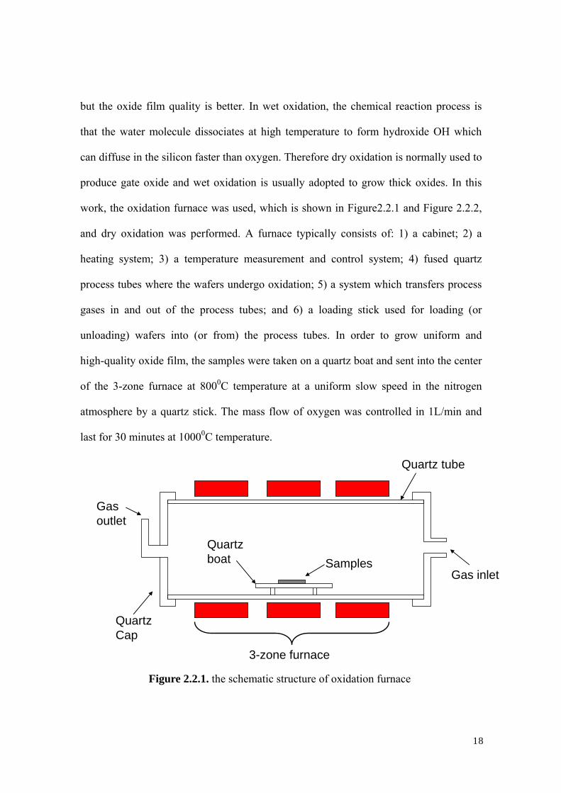
18
but the oxide film quality is better. In wet oxidation, the chemical reaction process is
that the water molecule dissociates at high temperature to form hydroxide OH which
can diffuse in the silicon faster than oxygen. Therefore dry oxidation is normally used to
produce gate oxide and wet oxidation is usually adopted to grow thick oxides. In this
work, the oxidation furnace was used, which is shown in Figure2.2.1 and Figure 2.2.2,
and dry oxidation was performed. A furnace typically consists of: 1) a cabinet; 2) a
heating system; 3) a temperature measurement and control system; 4) fused quartz
process tubes where the wafers undergo oxidation; 5) a system which transfers process
gases in and out of the process tubes; and 6) a loading stick used for loading (or
unloading) wafers into (or from) the process tubes. In order to grow uniform and
high-quality oxide film, the samples were taken on a quartz boat and sent into the center
of the 3-zone furnace at 8000C temperature at a uniform slow speed in the nitrogen
atmosphere by a quartz stick. The mass flow of oxygen was controlled in 1L/min and
last for 30 minutes at 10000C temperature.
Gas inlet
Gas outlet
Quartz Cap
3-zone furnace
Quartz boat Samples
Quartz tube
Figure 2.2.1. the schematic structure of oxidation furnace
19
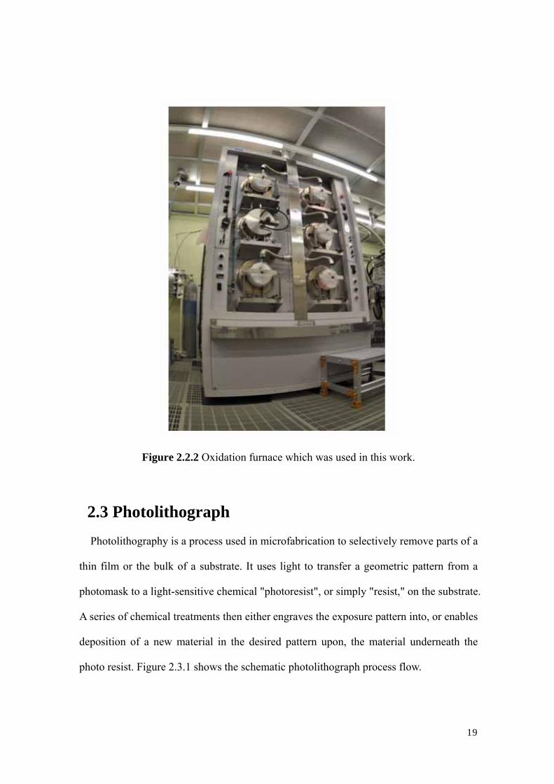
Figure 2.2.2 Oxidation furnace which was used in this work.
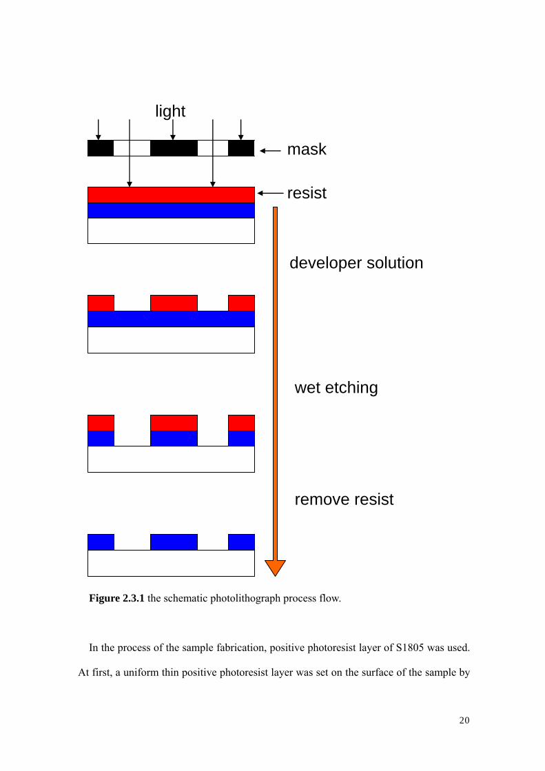
2.3 Photolithograph Photolithography is a process used in microfabrication to selectively remove parts of a
thin film or the bulk of a substrate. It uses light to transfer a geometric pattern from a
photomask to a light-sensitive chemical "photoresist", or simply "resist," on the substrate.
A series of chemical treatments then either engraves the exposure pattern into, or enables
deposition of a new material in the desired pattern upon, the material underneath the
photo resist. Figure 2.3.1 shows the schematic photolithograph process flow.
20
mask
resist
light
developer solution
wet etching
remove resist
Figure 2.3.1 the schematic photolithograph process flow.
In the process of the sample fabrication, positive photoresist layer of S1805 was used.
At first, a uniform thin positive photoresist layer was set on the surface of the sample by
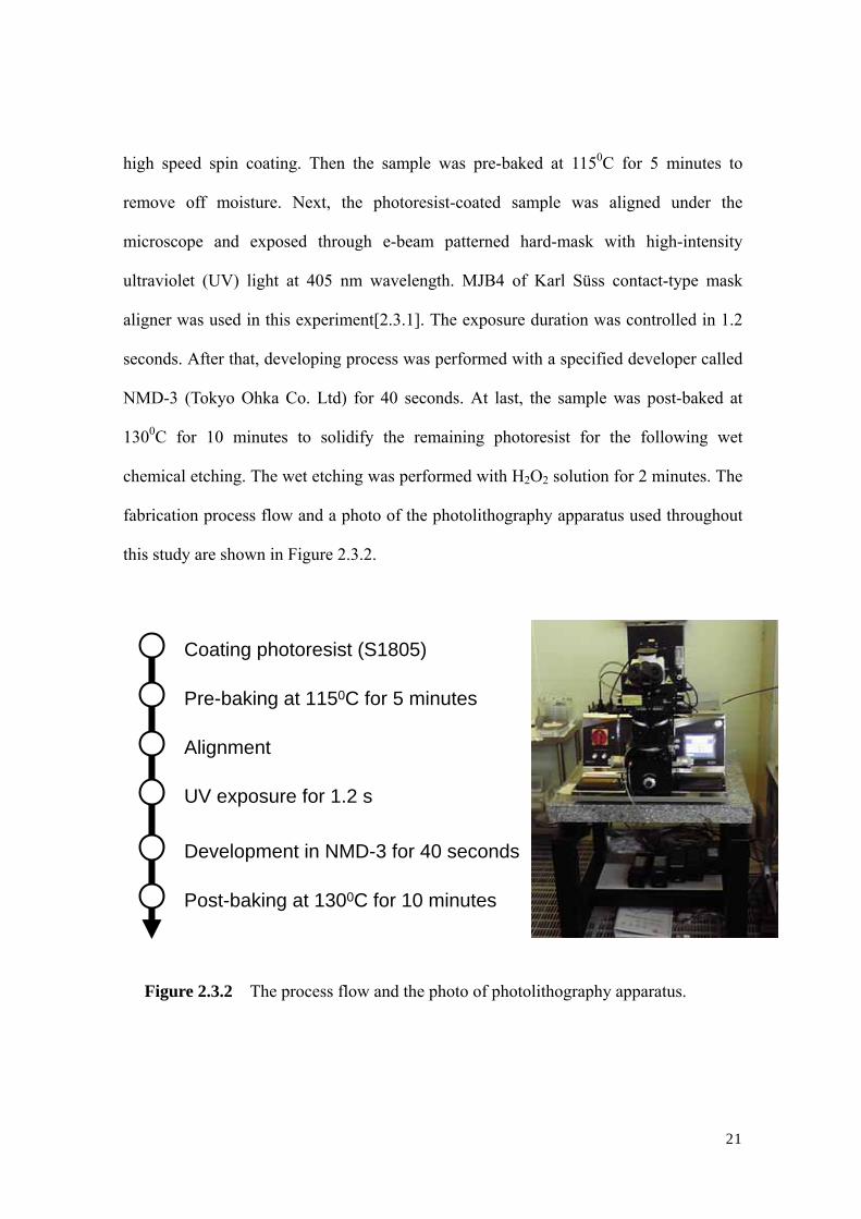
21
high speed spin coating. Then the sample was pre-baked at 1150C for 5 minutes to
remove off moisture. Next, the photoresist-coated sample was aligned under the
microscope and exposed through e-beam patterned hard-mask with high-intensity
ultraviolet (UV) light at 405 nm wavelength. MJB4 of Karl Süss contact-type mask
aligner was used in this experiment[2.3.1]. The exposure duration was controlled in 1.2
seconds. After that, developing process was performed with a specified developer called
NMD-3 (Tokyo Ohka Co. Ltd) for 40 seconds. At last, the sample was post-baked at
1300C for 10 minutes to solidify the remaining photoresist for the following wet
chemical etching. The wet etching was performed with H2O2 solution for 2 minutes. The
fabrication process flow and a photo of the photolithography apparatus used throughout
this study are shown in Figure 2.3.2.
Coating photoresist (S1805)
Pre-baking at 1150C for 5 minutes
Alignment
UV exposure for 1.2 s
Development in NMD-3 for 40 seconds
Post-baking at 1300C for 10 minutes
Figure 2.3.2 The process flow and the photo of photolithography apparatus.

22
2.4 RF Magnetron Sputtering After thermal oxidation to form silicon dioxide, a 50 nm W film was deposited
by RF magnetron sputtering to form gate electrode. Sputtering is one of the vacuum
processes used to deposit ultra thin films of various materials on substrates and
extensively used in the semiconductor industry. A high voltage across a
low-pressure gas (usually argon at about 5 mTorr) is applied to create a “plasma”
which consists of electrons and gas ions in a high-energy state. Then the energized
plasma ions strike the “target” composed of the desired coating material, and cause
atoms of the target to be ejected with enough energy to travel to the substrate
surface. The sputtering process is schematically shown in Figure 2.4.1. The base
pressure of the sputtering chamber was controlled at 10-6 Pa during the substrate
transfer. Argon gas flow was set to 7sccm while holding the deposition chamber
pressure at of which was set to be 1.33Pa. The 150W RF current power was used to
produce plasma. Figure 2.4.2 shows the sputtering system used in this work.
Ar+
Sputtering Gas
Sample
Sputtering Target
Figure 2.4.1 the schematic of RF magnetron sputtering
23
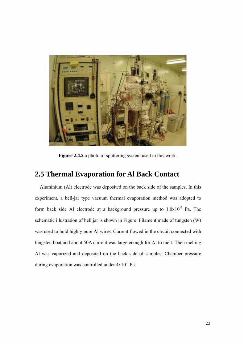
Figure 2.4.2 a photo of sputtering system used in this work.
2.5 Thermal Evaporation for Al Back Contact Aluminium (Al) electrode was deposited on the back side of the samples. In this
experiment, a bell-jar type vacuum thermal evaporation method was adopted to
form back side Al electrode at a background pressure up to 1.0x10⁻³ Pa. The
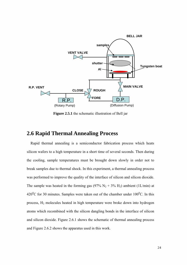
schematic illustration of bell jar is shown in Figure. Filament made of tungsten (W)
was used to hold highly pure Al wires. Current flowed in the circuit connected with
tungsten boat and about 50A current was large enough for Al to melt. Then melting
Al was vaporized and deposited on the back side of samples. Chamber pressure
during evaporation was controlled under 4x10⁻³ Pa.
24
D.P.FORE
ROUGHCLOSE
R.P.
R.P. VENT
shutter
AlTungsten boat
VENT VALVE
MAIN VALVE
BELL JAR
samples
(Diffusion Pump)(Rotary Pump)
Figure 2.5.1 the schematic illustration of Bell jar
2.6 Rapid Thermal Annealing Process Rapid thermal annealing is a semiconductor fabrication process which heats
silicon wafers to a high temperature in a short time of several seconds. Then during
the cooling, sample temperatures must be brought down slowly in order not to
break samples due to thermal shock. In this experiment, a thermal annealing process
was performed to improve the quality of the interface of silicon and silicon dioxide.
The sample was heated in the forming gas (97% N2 + 3% H2) ambient (1L/min) at
4200C for 30 minutes. Samples were taken out of the chamber under 1000C. In this
process, H2 molecules heated in high temperature were broke down into hydrogen
atoms which recombined with the silicon dangling bonds in the interface of silicon
and silicon dioxide. Figure 2.6.1 shows the schematic of thermal annealing process
and Figure 2.6.2 shows the apparatus used in this work.
25
Si-substrate
SiO2
Si Si Si Si Si Si
Dangling bonds
H+H+ H+
H+
H+
Si-substrate
SiO2
Si Si Si Si Si SiH H H H
Figure 2.6.1 the schematic illustration of thermal annealing
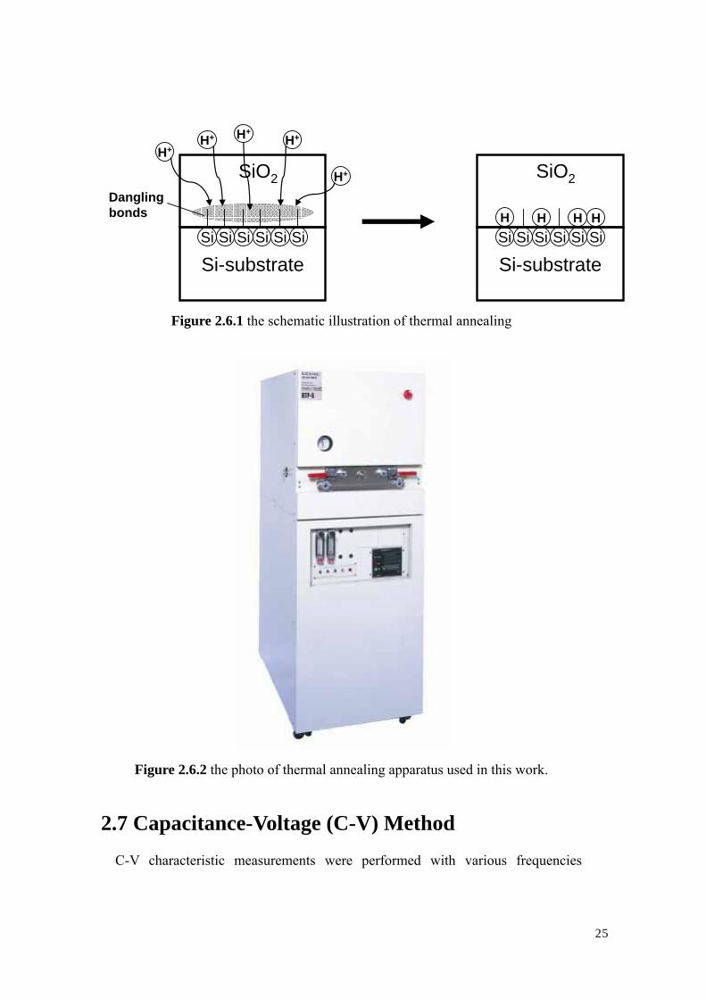
Figure 2.6.2 the photo of thermal annealing apparatus used in this work.
2.7 Capacitance-Voltage (C-V) Method C-V characteristic measurements were performed with various frequencies
26
(1KHz~1MHz) by precision LCR Meter (HP 4284A, Agilent). The energy band
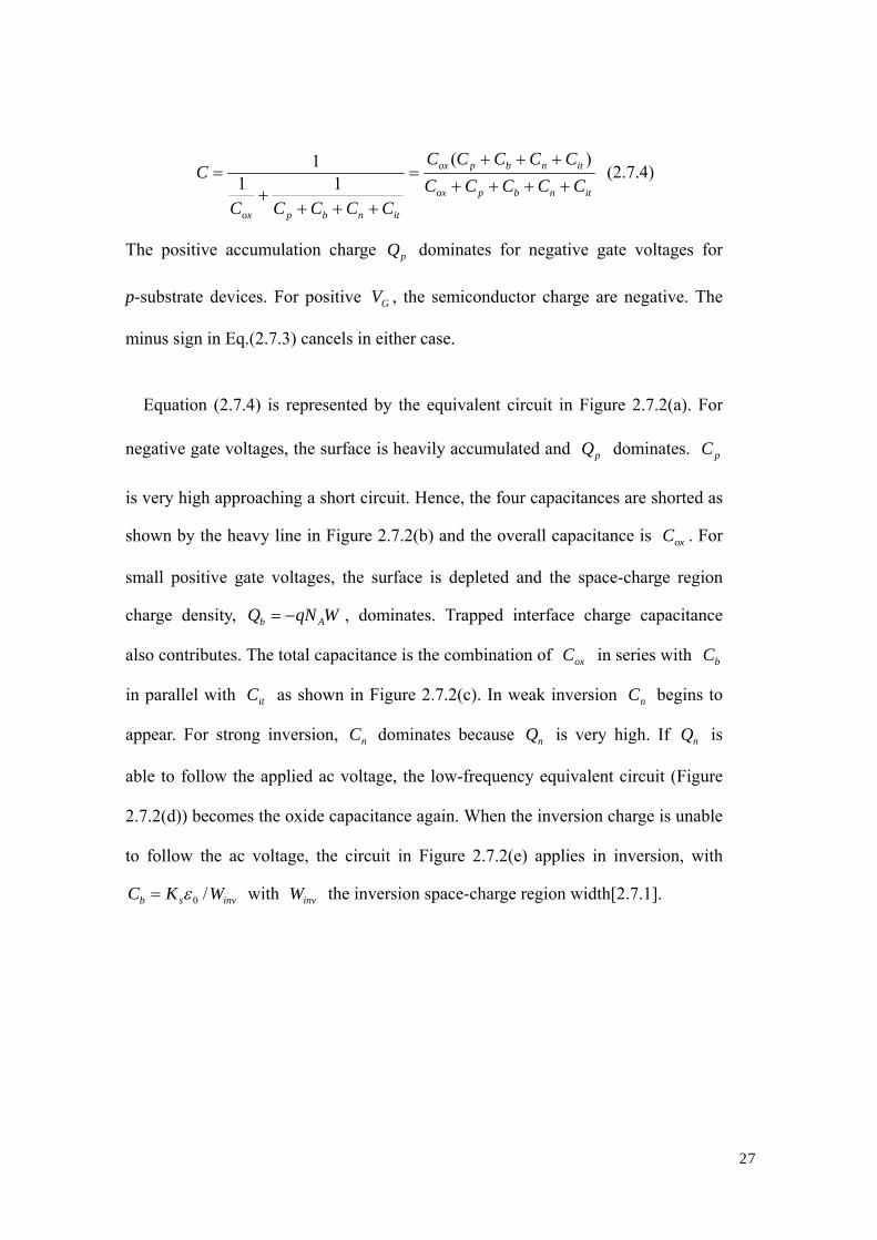
diagram of an MOS capacitor on a p-type substrate is shown in figure 2.7.1. The
intrinsic energy level Ei or potential φin the neutral part of device is taken as the
zero reference potential. The surface potential φs is measured from this reference
level. The capacitance is defined as
dVdQC = (2.7.1)
It is the change of charge due to a change of voltage and is most commonly given in
units of farad/unit area. During capacitance measurements, a small-signal ac voltage
is applied to the device. The resulting charge variation gives rise to the capacitance.
Looking at an MOS-C from the gate, GG dVdQC /= , where GQ and GV are the
gate charge and the gate voltage. Since the total charge in the device must be zero,
)( itsG QQQ +−= assuming no oxide charge. The gate voltage is partially dropped
across the oxide and partially across the semiconductor. This gives
soxFBG VVV φ++= , where FBV is the flatband voltage, oxV the oxide voltage, and
sφ the surface potential, allowing Eq.(2.7.1) to be rewritten as
sox
its
ddVdQdQC
φ++
−= (2.7.2)
The semiconductor charge density sQ , consists of hole charge density pQ ,
space-charge region bulk charge density bQ , and electron charge density nQ . With
nbps QQQQ ++= , Eq.(2.7.2) becomes
itnbp
s
its
ox
dQdQdQdQd
dQdQdVC
++++
+
−= φ1 (2.7.3)
Utilizing the general capacitance definition of Eq.(2.7.1), Eq.(2.7.3) becomes
27
itnbpox
itnbpox
itnbpox
CCCCCCCCCC
CCCCC
C++++
+++=
++++
=)(
111 (2.7.4)
The positive accumulation charge pQ dominates for negative gate voltages for
p-substrate devices. For positive GV , the semiconductor charge are negative. The
minus sign in Eq.(2.7.3) cancels in either case.
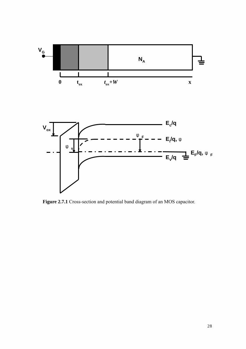
Equation (2.7.4) is represented by the equivalent circuit in Figure 2.7.2(a). For
negative gate voltages, the surface is heavily accumulated and pQ dominates. pC
is very high approaching a short circuit. Hence, the four capacitances are shorted as
shown by the heavy line in Figure 2.7.2(b) and the overall capacitance is oxC . For
small positive gate voltages, the surface is depleted and the space-charge region
charge density, WqNQ Ab −= , dominates. Trapped interface charge capacitance
also contributes. The total capacitance is the combination of oxC in series with bC
in parallel with itC as shown in Figure 2.7.2(c). In weak inversion nC begins to
appear. For strong inversion, nC dominates because nQ is very high. If nQ is
able to follow the applied ac voltage, the low-frequency equivalent circuit (Figure
2.7.2(d)) becomes the oxide capacitance again. When the inversion charge is unable
to follow the ac voltage, the circuit in Figure 2.7.2(e) applies in inversion, with
invsb WKC /0ε= with invW the inversion space-charge region width[2.7.1].
28
VG
NA
0 tox tox+W x
Vox
φs
φF
Ec/q
Ei/q, φ
Ev/qEF/q, φF
Figure 2.7.1 Cross-section and potential band diagram of an MOS capacitor.
29
Cox
Cp Cb Cn Cit
Cox
Cp Cb Cn Cit
Cox
Accumulation
(b)
Cox
Cp Cb Cn Cit
Cox
CbCit
Depletion
(c)
Cox
Cp Cb Cn Cit
Cox
Inversion- Low Frequency
(d)
Cox
Cp CbCn Cit
Cox
Cb
Inversion- High Frequency
(e)
(a)
Figure 2.7.2 Capacitance of an MOS capacitor for various bias condition.
2.8 Conductance Method The conductance method was proposed by Nicollian and Goetzberger in 1967
and is one of the most sensitive methods to determine Dit. Interface trap densities of
109 cm-2eV-1 and lower can be measured. It can give information about Dit in the
depletion and weak inversion, the capture cross-section of majority carriers and the
surface potential fluctuations. The conductance method is to measure the equivalent
parallel conductance Gp of an MOS-C as a function of bias voltage and frequency.
Conductance Gp represents the loss mechanism caused by interface trap capture and
emission of carriers, which is a measure of interface state density. Figure 2.8.1(a)
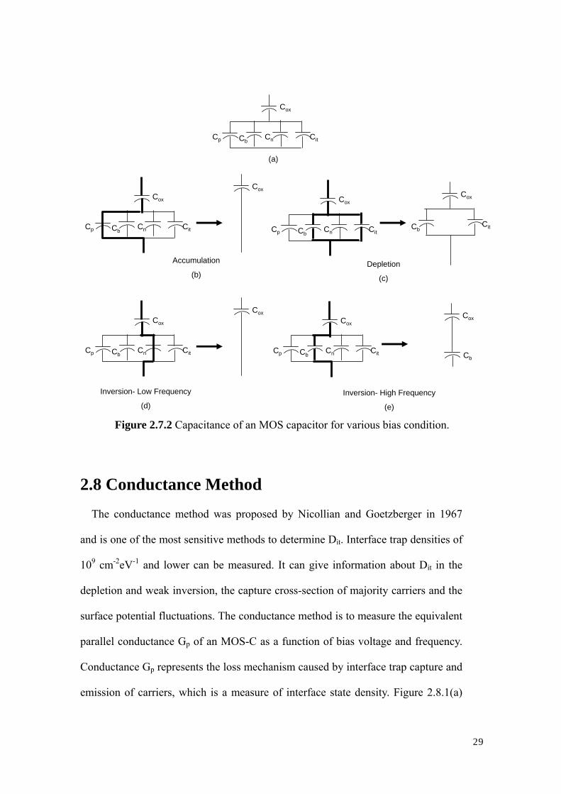
30
shows the simplified equivalent circuit of an MOS-C. Cox is the oxide capacitance,
CS is the semiconductor capacitance, Cit is the interface trap capacitance and Rit is
the lossy process caused by the capture-emission of carriers due to interface state
density.
Cox
CS
Cit
Rit
•
•
Cox
CP GP
•
•
Cm Gm
•
•(a) (b) (c)
Figure 2.8.1 Equivalent circuits for conductance measurement. (a) MOS-C with
interface trap time constant, (b) simplified circuit, (c) measured circuit
The circuit of Figure 2.8.1(a) can be simplified by the circuit of Figure 2.8.1(b).
Cp and Gp are represented by Eq. (2.8.1) and (2.8.2).
2)(1 it
itSp
CCCωτ+
+= (2.8.1)
2)(1 it
ititp DqGωτ
ωτω +
= (2.8.2)
where Cit=q2Dit, ω=2πf (f=measurement frequency) and τit=RitCit, the interface trap
time constant, given by τit=[vthσpNAexp(-qφs/kT]-1. Dividing Gp by ω makes Eq.
(2.8.2) symmetrical in ωτit. Equation (2.8.1) and (2.8.2) are for interface traps with a
single energy level in the band gap. Interface traps at the SiO2-Si interface, however,
are continuously distributed in energy throughout the Si band gap. Capture and
emission occurs primarily by traps located within a few kT/q above and below the
31
Fermi level, leading to a time constant dispersion and giving the normalized
conductance as
])(1ln[2
2it
it
itp qDGωτ
ωτω+= (2.8.3)
Equations (2.8.2) and (2.8.3) show that the conductance is easier to interpret than
the capacitance, because Eq.(2.8.2) does not require CS. The conductance is
measured as a function of frequency and plotted as Gp/ω versus ω. Gp/ω has a
maximum at ω=1/τit and at that maximum Dit =2 Gp/qω. For Eq.(2.8.3) we find
itτω /2≈ and Dit=2.5 Gp/qω at the maximum. Hence we determine Dit from the
maximum Gp/ω and determine τit from ω at the peak conductance location on the
ω-axis.
Experimental Gp/ω versus ω curves are generally broader than predicted by
Eq(2.8.3). attributed to interface trap time constant dispersion caused by surface
potential fluctuations due to non-uniformities in oxide charge and interface traps as
well as doping density. Surface potential fluctuations are more pronounced in p-Si
than in n-Si. Surface potential fluctuations complicate the analysis of the
experimental data. When such fluctuations are taken into account, Eq(2.8.3)
becomes
ssitit
itp dUUPDqG)(])(1ln[
22ωτ
ωτω+= ∫
∞
∞
(2.8.4)
where P(Us) is a probability distribution of the surface potential fluctuation given by
)2
)(exp(2
1)( 2
2
2 σπσss
sUUUP −
−= (2.8.5)
with SU and σthe normalized mean surface potential and standard deviation,
32
respectively. An approximate expression giving the interface trap density in terms
of the measured maxium conductance is
max
5.2⎟⎠⎞
⎜⎝⎛≈
ωP
itG
qD (2.8.6)
Capacitance meters generally assume the device to consist of the parallel Cm-Gm
combination in Figure 2.8.1(c). A circuit comparison of Figure 2.8.1(b) to 2.8.1(c)
gives Gp/ω in terms of the measured capacitance Cm, the oxide capacitance, and the
measured conductance Gm as
222
2
)( moxm
oxmP
CCGCGG
−+=
ωω
ω (2.8.7)
assuming negligible series resistance. The conductance measurement must be carried out
over a wide frequency range. The portion of the band gap probed by conductance
measurements is typically from flatband to weak inversion. The measurement frequency
should be accurately determined and the signal amplitude should be kept at around
50mV or less to prevent harmonics of the signal frequency giving rise to spurious
conductances. The conductance depends only on the device area for a given Dit.
However, a capacitor with thin oxide has a high capacitance relative to the conductance,
especially for low Dit and the resolution of the capacitance meter is dominated by the
out-of-phase capacitive current component. Reducing Cox by increasing the oxide
thickness helps this measurement problem[2.7.1].
2.9 Quasi-static Method The low-frequency or quasi-static method is a common interface trapped charge
measurement method. It provides information only on the interface trapped charge
density, but not on their capture cross-sections. The basic theory of the quasi-static
33
method was developed by Berglund. The method compares a low-frequency C–V curve
with one free of interface traps. The latter can be a theoretical curve, but is usually an hf
C–V curve determined at a frequency where interface traps are assumed not to respond.
“Low frequency” means that interface traps and minority carrier inversion charges must
be able to respond to the measurement ac probe frequency. The interface trap response
has similar limitations. Fortunately, the limitations are usually less severe than for
minority carrier response and frequencies low enough for inversion layer response are
generally low enough for interface trap response.
The lf capacitance is given by Eq. (2.9.1) in depletion-inversion as
1)11( −
++=
itSoxlf CCC
C (2.9.1)
CS is the lf semiconductor capacitance, Cit is related to the interface trap density Dit by
Dit = Cit/q2, giving
)(12 S
lfox
lfoxit C
CCCC
qD −
−= (2.9.2)
Equation (2.9.2) is suitable for interface trap density determination over the entire
band gap.
Clf and CS must be known to determine Dit . Clf is measured as a function of gate
voltage and the calculation of CS is simplified by Castagn´e and Vapaillen who proposed
a method to eliminate the uncertainty associated with the calculation of CS and gave the
Equation (2.9.3):
hfox
hfoxS CC
CCC
−= (2.9.3)
Substituting Eq. (2.9.3) into (2.9.2) gives Dit in terms of the measured lf and hf C–V
curves as
34
)/1
//1
/(2
oxhf
oxhf
oxlf
oxlfoxit CC
CCCC
CCqC
D−
−−
= (2.9.4)
Equation (2.9.4) gives Dit over only a limited range of the band gap, typically from the
onset of inversion, but not strong inversion, to a surface potential towards the majority
carrier band edge where the ac measurement frequency equals the inverse of the
interface trap emission time constant. This corresponds to an energy about 0.2 eV from
the majority carrier band edge. The higher the frequency the closer to the band edge can
be probed[2.7.1].
2.10 Scanning Electron Microscopy (SEM) Method Fin structures were observed by scanning electron microscope (SEM).
An electron microscope uses an electron beam (e-beam) to produce a magnified image
of the sample. The three principal electron microscopes are: scanning, transmission and
emission. In the scanning and transmission electron microscope, an electron beam
incident on the sample produces an image while in the field-emission microscope the
specimen itself is the source of electrons. A scanning electron microscope consists of an
electron gun, a lens system, scanning coils, an electron collector, and a cathode ray
display tube (CRT). The electron energy is typically 10–30 keV for most samples. The
use of electrons has two main advantages over optical microscopes: much larger
magnifications are possible since electron wavelengths are much smaller than photon
wavelengths and the depth of field is much higher. De Broglie proposed in 1923 that
particles can also behave as waves. The electron wavelength λe depends on the electron
velocity v or the accelerating voltage V as
(2.10.1) ][22.12
nmVqmV
hmvh
e ===λ
35
λe = 0.012 nm for V = 10, 000 V—a wavelength significantly below the 400 to 700 nm
wavelengths of visible light—making the resolution of an SEM much better than that of
an optical microscope[2.7.1].
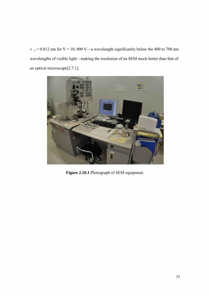
Figure 2.10.1 Photograph of SEM equipment.
36
Virtual Source
First Condenser Lens
Condenser Aperture
Objective Aperture
Second Condenser Lens
Scan Coils
Objective Lens
Sample
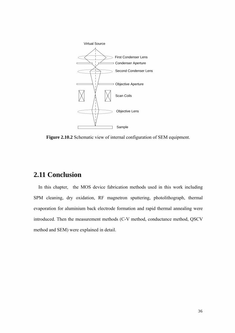
Figure 2.10.2 Schematic view of internal configuration of SEM equipment.
2.11 Conclusion In this chapter, the MOS device fabrication methods used in this work including
SPM cleaning, dry oxidation, RF magnetron sputtering, photolithograph, thermal
evaporation for aluminium back electrode formation and rapid thermal annealing were
introduced. Then the measurement methods (C-V method, conductance method, QSCV
method and SEM) were explained in detail.

37
Refernces
[2.1.1] Wemer Kern, The Evolution of Silicon Wafer Cleaning Technology, J.
Electronchem. Soc., Vol. 137, No.6, June 1990
[2.3.1] http://www.suss.com
[2.7.1] D. Schroder, Semiconductor material and device characterization, 3rd edition, p.
347-350, Willey Interscience, NJ (2006).
38
Chapter3 Interface State Density Extraction of
Three-Dimensional Channel Structure
3.1 Device Fabrication Process
3.2 Analysis of Fin Structure with SEM Images
3.3 Analysis of C-V Curves
39
3.4 Extraction of Interface State Density of planar and Fin
devices by Quasi-static C-V Method
3.5 Extraction of Interface State Density of planar devices by
Conductance Method
3.6 Conclusion of This Chapter
References
40
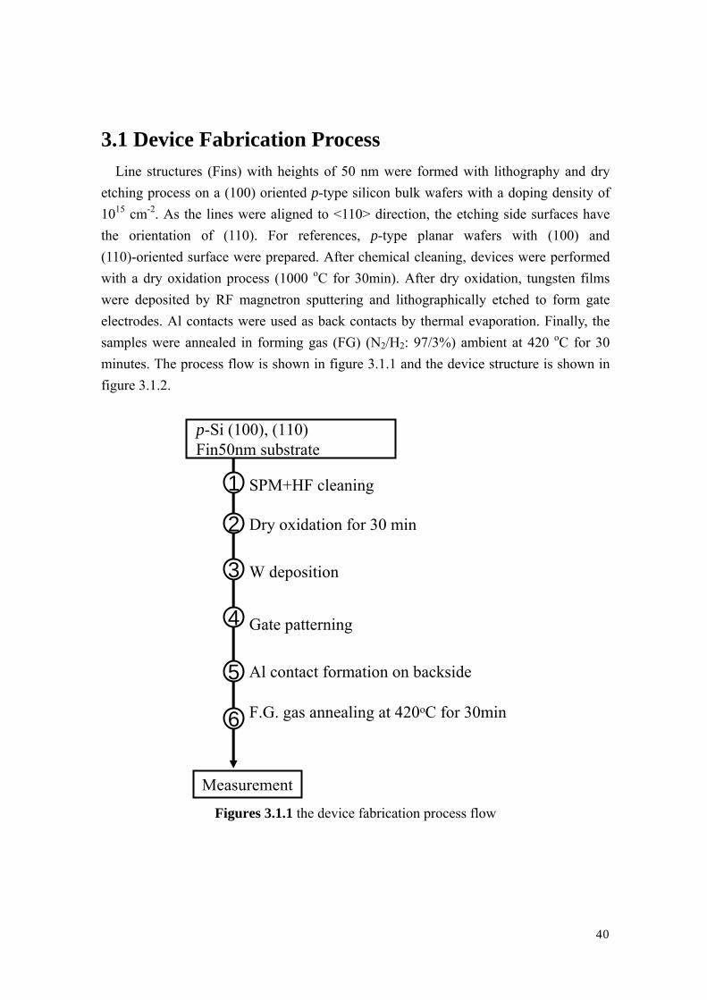
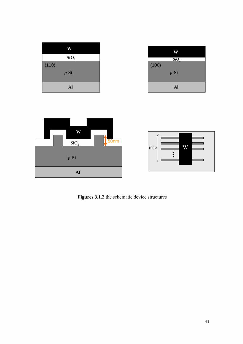
3.1 Device Fabrication Process Line structures (Fins) with heights of 50 nm were formed with lithography and dry
etching process on a (100) oriented p-type silicon bulk wafers with a doping density of 1015 cm-2. As the lines were aligned to <110> direction, the etching side surfaces have the orientation of (110). For references, p-type planar wafers with (100) and (110)-oriented surface were prepared. After chemical cleaning, devices were performed with a dry oxidation process (1000 oC for 30min). After dry oxidation, tungsten films were deposited by RF magnetron sputtering and lithographically etched to form gate electrodes. Al contacts were used as back contacts by thermal evaporation. Finally, the samples were annealed in forming gas (FG) (N2/H2: 97/3%) ambient at 420 oC for 30 minutes. The process flow is shown in figure 3.1.1 and the device structure is shown in figure 3.1.2.
1 SPM+HF cleaning
p-Si (100), (110)Fin50nm substrate
3
4
5
6
2 Dry oxidation for 30 min
W deposition
Gate patterning
Al contact formation on backside
F.G. gas annealing at 420oC for 30min
Measurement
Figures 3.1.1 the device fabrication process flow
41
Al
SiO2
p-Si
W
Al
p-Si
SiO2
W
Al
SiO2
p-Si
W
(110) (100)
50nmW
•••
100
Figures 3.1.2 the schematic device structures
42
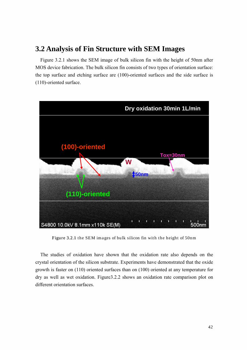
3.2 Analysis of Fin Structure with SEM Images Figure 3.2.1 shows the SEM image of bulk silicon fin with the height of 50nm after
MOS device fabrication. The bulk silicon fin consists of two types of orientation surface: the top surface and etching surface are (100)-oriented surfaces and the side surface is (110)-oriented surface.
50nm
Tox=30nmW
(100)-oriented
(110)-oriented
Dry oxidation 30min 1L/min
Figure 3.2.1 the SEM images of bulk silicon fin with the height of 50nm
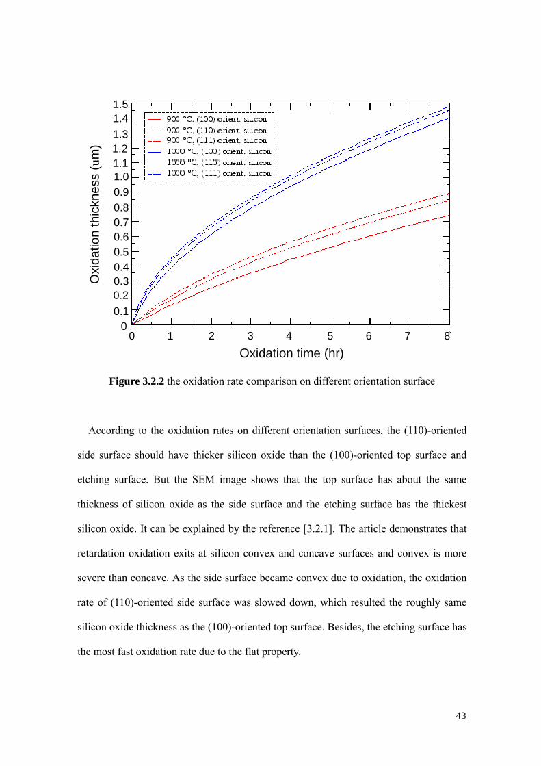
The studies of oxidation have shown that the oxidation rate also depends on the
crystal orientation of the silicon substrate. Experiments have demonstrated that the oxide growth is faster on (110) oriented surfaces than on (100) oriented at any temperature for dry as well as wet oxidation. Figure3.2.2 shows an oxidation rate comparison plot on different orientation surfaces.
43
0 1 2 3 4 5 6 7 8Oxidation time (hr)
00.10.20.30.40.50.60.70.80.91.01.11.21.31.41.5
Oxi
datio
n th
ickn
ess
(um
)
Figure 3.2.2 the oxidation rate comparison on different orientation surface
According to the oxidation rates on different orientation surfaces, the (110)-oriented
side surface should have thicker silicon oxide than the (100)-oriented top surface and
etching surface. But the SEM image shows that the top surface has about the same
thickness of silicon oxide as the side surface and the etching surface has the thickest
silicon oxide. It can be explained by the reference [3.2.1]. The article demonstrates that
retardation oxidation exits at silicon convex and concave surfaces and convex is more
severe than concave. As the side surface became convex due to oxidation, the oxidation
rate of (110)-oriented side surface was slowed down, which resulted the roughly same
silicon oxide thickness as the (100)-oriented top surface. Besides, the etching surface has
the most fast oxidation rate due to the flat property.
44
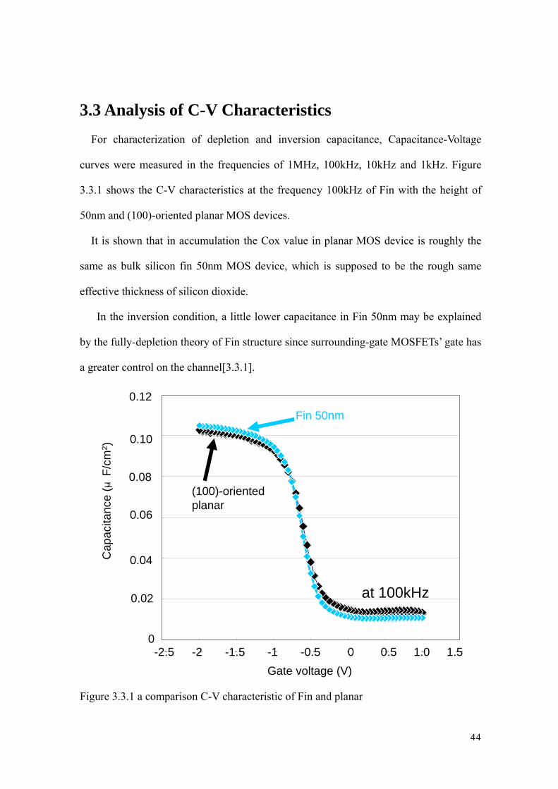
3.3 Analysis of C-V Characteristics For characterization of depletion and inversion capacitance, Capacitance-Voltage
curves were measured in the frequencies of 1MHz, 100kHz, 10kHz and 1kHz. Figure
3.3.1 shows the C-V characteristics at the frequency 100kHz of Fin with the height of
50nm and (100)-oriented planar MOS devices.
It is shown that in accumulation the Cox value in planar MOS device is roughly the
same as bulk silicon fin 50nm MOS device, which is supposed to be the rough same
effective thickness of silicon dioxide.
In the inversion condition, a little lower capacitance in Fin 50nm may be explained
by the fully-depletion theory of Fin structure since surrounding-gate MOSFETs’ gate has
a greater control on the channel[3.3.1].
0.00E+00
2.00E-08
4.00E-08
6.00E-08
8.00E-08
1.00E-07
1.20E-07
-2.5 -2 -1.5 -1 -0.5 0 0.5 1 1.5-2 -1 0 1.00
0.04
0.08
0.12
Cap
acita
nce
(μF/
cm2 )
Gate voltage (V)
(100)-oriented planar
Fin 50nm
-2.5 -1.5 -0.5 0.5 1.5
0.02
0.06
0.10
at 100kHz
Figure 3.3.1 a comparison C-V characteristic of Fin and planar
45
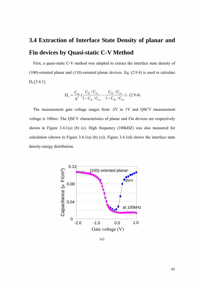
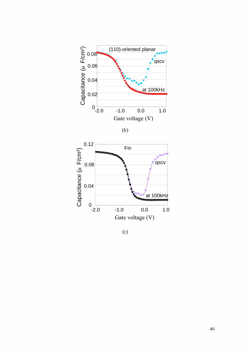
3.4 Extraction of Interface State Density of planar and
Fin devices by Quasi-static C-V Method First, a quasi-static C-V method was adopted to extract the interface state density of
(100)-oriented planar and (110)-oriented planar devices. Eq. (2.9.4) is used to calculate
Dit [3.4.1].
)/1
//1
/(2
oxhf
oxhf
oxlf
oxlfoxit CC
CCCC
CCqC
D−
−−
= (2.9.4)
The measurement gate voltage ranges from -2V to 1V and QSCV measurement
voltage is 100mv. The QSCV characteristics of planar and Fin devices are respectively
shown in Figure 3.4.1(a) (b) (c). High frequency (100kHZ) was also measured for
calculation (shown in Figure 3.4.1(a) (b) (c)). Figure 3.4.1(d) shows the interface state
density energy distribution.
0.00E+00
2.00E-08
4.00E-08
6.00E-08
8.00E-08
1.00E-07
1.20E-07
-2.00E+00 -1.50E+00 -1.00E+00 -5.00E-01 0.00E+00 5.00E-01 1.00E+00
Cap
acita
nce
(μF/
cm2 )
0
0.04
0.08
0.12(100)-oriented planar
at 100kHz
qscv
-2.0 -1.0 0.0Gate voltage (V)
1.0
(a)
46
0.00E+00
1.00E-08
2.00E-08
3.00E-08
4.00E-08
5.00E-08
6.00E-08
7.00E-08
8.00E-08
9.00E-08
-2.00E+00 -1.50E+00 -1.00E+00 -5.00E-01 0.00E+00 5.00E-01 1.00E+00
at 100kHz
qscv
(110)-oriented planar
-2.0 -1.0 0.0 1.0Gate voltage (V)
0
0.02
0.06
0.04
0.08
Cap
acita
nce
(μF/
cm2 )
(b)
Cap
acita
nce
(μF/
cm2 )
0.00E+00
2.00E-08
4.00E-08
6.00E-08
8.00E-08
1.00E-07
1.20E-07
-2.00E+00 -1.50E+00 -1.00E+00 -5.00E-01 0.00E+00 5.00E-01 1.00E+00
Gate voltage (V)-2.0 0.0 1.0-1.0
0
0.04
0.08
0.12Fin
qscv
at 100kHz
(c)
47
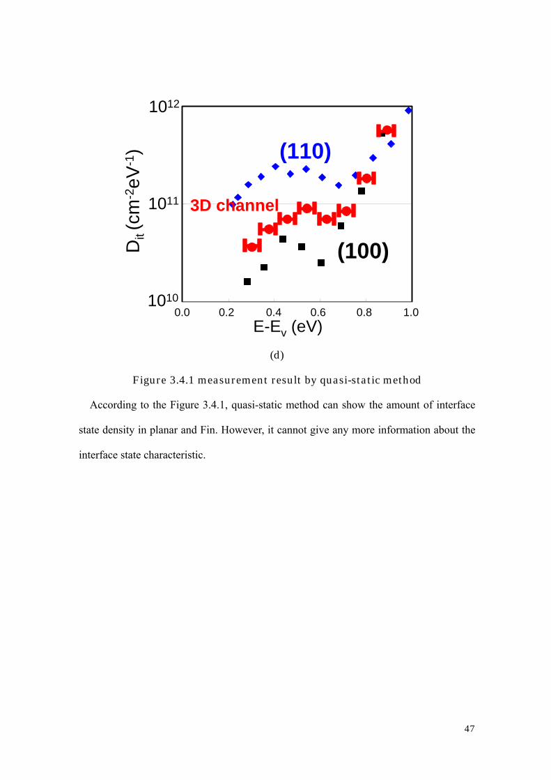
Dit(c
m-2
eV-1
) (110)
(100)
0.0 0.2 0.4 0.6 0.8 1.0E-Ev (eV)
3D channel
1010
1011
1012
(d)
Figure 3.4.1 measurement result by quasi-static method
According to the Figure 3.4.1, quasi-static method can show the amount of interface
state density in planar and Fin. However, it cannot give any more information about the
interface state characteristic.
48
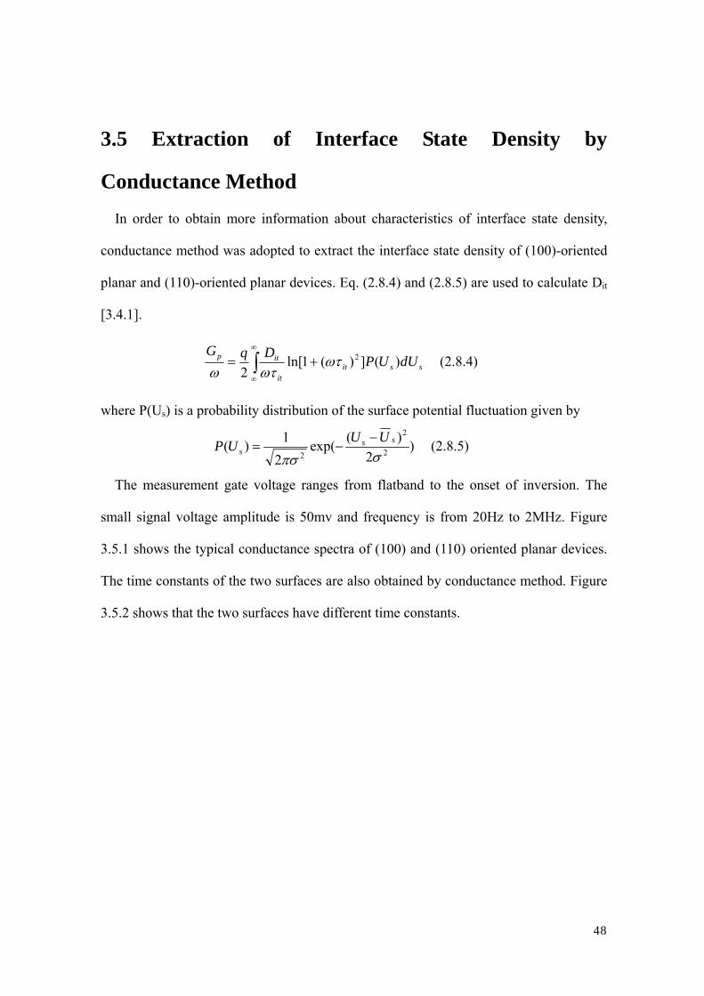
3.5 Extraction of Interface State Density by
Conductance Method In order to obtain more information about characteristics of interface state density,
conductance method was adopted to extract the interface state density of (100)-oriented
planar and (110)-oriented planar devices. Eq. (2.8.4) and (2.8.5) are used to calculate Dit
[3.4.1].
ssitit
itp dUUPDqG)(])(1ln[
22ωτ
ωτω+= ∫
∞
∞
(2.8.4)
where P(Us) is a probability distribution of the surface potential fluctuation given by
)2
)(exp(2
1)( 2
2
2 σπσss
sUUUP −
−= (2.8.5)
The measurement gate voltage ranges from flatband to the onset of inversion. The
small signal voltage amplitude is 50mv and frequency is from 20Hz to 2MHz. Figure
3.5.1 shows the typical conductance spectra of (100) and (110) oriented planar devices.
The time constants of the two surfaces are also obtained by conductance method. Figure
3.5.2 shows that the two surfaces have different time constants.
49
0.00E+00
1.00E-09
2.00E-09
3.00E-09
4.00E-09
5.00E-09
6.00E-09
7.00E-09
8.00E-09
9.00E-09
1.00E-08
1.00E+01 1.00E+02 1.00E+03 1.00E+04 1.00E+05 1.00E+06 1.00E+07
Frequency (Hz)101 103 105 107
0
5x10⁻⁹
1x10⁻⁸
Gp/ω
(F/c
m2 )
(100)
0 .00E+00
5 .00E-09
1 .00E-08
1 .50E-08
2 .00E-08
2 .50E-08
3 .00E-08
3 .50E-08
4 .00E-08
4 .50E-08
5 .00E-08
1 .00E+01 1 .00E+02 1 .00E+03 1 .00E+04 1 .00E+05 1 .00E+06 1 .00E+07
101 103 105 107
Frequency (Hz)
0
2x10⁻⁸
Gp/
ω(F
/cm
2 )
4x10⁻⁸
(110)
Figure 3.5.1 the typical conductance spectra of (100) and (110) oriented surfaces.

50
1 . 0 0E- 0 7
1 . 0 0E- 0 6
1 . 0 0E- 0 5
1 . 0 0E- 0 4
1 . 0 0E- 0 3
1 . 0 0E- 0 2
1 . 0 0E- 0 1
1 . 0 0E+ 0 0
0 .0 0 E+ 0 0 5 . 0 0 E- 0 2 1 . 0 0 E- 0 1 1 . 5 0 E- 0 1 2 . 0 0 E- 0 1 2 . 5 0 E- 0 1 3 . 0 0 E- 0 1 3 . 5 0 E- 0 1 4 . 0 0 E- 0 1 4 . 5 0E- 0 10.0 0.3 0.5
Surface potential (eV)
Tim
e co
nsta
nt (s
)
10-7
10-5
10-3
10-1
(100)
(110)
Figure 3.5.2 different time constants of (100) and (110) oriented surfaces.
0.00E+00
5.00E+10
1.00E+11
1.50E+11
2.00E+11
2.50E+11
3.00E+11
3.50E+11
0.00E+00 1.00E-01 2.00E-01 3.00E-01 4.00E-01 5.00E-01 6.00E-01 7.00E-010.0 0.2 0.4 0.6 0.8
1x10-11
2x10-11
3x10-11
Dit(c
m-2
eV-1
)
Surface potential (eV)
(110)
(100)
conductance QSCV
Figure 3.5.3 a comparison of interface state density of the two surfaces with
quasi-static method and conductance method.
Then a comparison of the energy distributions of the interface state density of the two
planar devices by the two methods is given in Figure 3.5.3. The surface potential
fluctuations of (100) and (110) oriented surfaces are different, which are respectively
about 0.05 and 0.07. From the comparison, it shows that the interface state densities
measured by the two methods are comparable.
51
3.6 Conclusion of This Chapter In this chapter, quasi-static method is adopted to extract interface state density of
planar and Fin. Then conductance method is adopted to extract interface state density of
planar devices. This method also gave time constant information of the two planar
devices. A comparison of interface state density of the two planar devices by the two
methods is conducted and shows comparable Dit value.
52
Reference
[3.2.1] DAH-BIN KAO, et al.,IEEE Transactions on electron devices,VOL. ED-34,
NO.5, MAY 1987.
[3.3.1] Christopher P. Auth, IEEE ELECTRON DEVICE LETTERS, VOL.18, NO.2,
February 1997.
[3.4.1] D. Schroder, Semiconductor material and device characterization, 3rd edition, p.
347-350, Willey Interscience, NJ (2006).
53
Chapter4 Modeling of Conductance Spectra by
Deconvolution
4.1 Numerical simulation of surface potential of 3D channel
4.2 Deconvolution of Conductance Spectra of Fin Devices
4.3 Conclusion of This Chapter
References
54
4.1 Numerical simulation of surface potential of
3D channel Because of different oxidation rates of (100) and (110) oriented planar surfaces,
different surface potentials may co-exist within the channel for 3D channel device. So it
is necessary to conduct a simulation of surface potential of 3D channel to obtain the
surface potential distribution. Figure 4.1.1 shows the simulation results. We choose one
point from top and side surfaces.
Extract surface potentials from these two points
55
-5.00E-02
0.00E+00
5.00E-02
1.00E-01
1.50E-01
2.00E-01
2.50E-01
3.00E-01
3.50E-01
-0.6 -0.5 -0.4 -0.3 -0.2 -0.1 0-0.6 -0.5 -0.4 -0.3 -0.2 -0.1 00
0.1
0.2
0.3
Gate voltage(V)
Sur
face
Pot
entia
l (eV
)
top
side
Figure 4.1.1 the simulation result of surface potential in top and side surfaces.
4.2 Deconvolution of Conductance Spectra of Fin
Devices Due to the higher surface potential of 30meV in top than side surface, a modeling of
conductance spectra by deconvolution has been proposed. We choose the conductance
spectra of (100) oriented surface in ψs = 0.036 and (110) oriented surface in ψs=
0.007. Then a fitting process of Fin is done with the two surfaces. Figure 4.2.1 shows a
rough fitting result. It showed a roughly agreement of conductance spectra between the
experiment data and fitting data of Fin, which demonstrates that the electrical response
of Dit with 3D surface can be roughly modeled with two planar surfaces[4.1.1]. In the
fitting process, 80% component of (100) oriented and 20% component of (110) oriented
surfaces are observed. It coincided the area ratios of top and side surfaces in the total

56
area showed in SEM image. It demonstrated that interface state density of Fin may be
expressed by weighted average of the two surfaces.
0.00E+00
1.00E-09
2.00E-09
3.00E-09
4.00E-09
5.00E-09
6.00E-09
7.00E-09
8.00E-09
9.00E-09
1.00E-08
1.00E+01 1.00E+02 1.00E+03 1.00E+04 1.00E+05 1.00E+06 1.00E+07
101 103 105 107
5x10⁻⁹
1x10⁻⁸
Gp/ω
(F/c
m2 )
Frequency (Hz)
0
Fin
(100) component
(110) component
Figure 4.2.2 the fitting results of conductance spectra of Fin
4.3 Conclusion of This Chapter A modeling of conductance spectra by deconvolution has been proposed in this study.
Fitting results show that the conductance spectra can be roughly expressed by weighted
average of the two surfaces. Based on the above analysis it is suggested that the
electrical response of interface state with three-dimensional surface can be roughly
modeled with two interface state of planar
57
References [4.1.1] S. Ogata, et al., Applied Physics Letters, Volume 98, Issue 9, p. 092906-092906-3
(2011)
58
Chapter5 5.1 Conclusion of This Study
In this study, we evaluate the interface state density of silicon bulk Fin devices with
different channel orientations. Two methods have been adopted in this study to obtain
characteristics of interface state density of three-dimensional MOS devices. One is
quasi-static capacitance-voltage method and the other is conductance method. By
comparison of the results obtained by these two methods, an evaluation of interface
state density in three-dimensional devices has been proposed.
At first, the interface state density of (100)-oriented and (110)-oriented planar devices
and Fin have been investigated by quasi-static method. Then the extraction of the
interface state density of planar surfaces has been done again by conductance method.
The two methods showed the similar energy distribution of interface state density.
Through comparison of time constant of planar devices, a difference has been found.
Then a modeling of conductance spectra by deconvolution has been proposed in this
study. The fitting results showed that conductance spectra of Fin can be roughly
expressed by weighted average of the two surfaces.
Based on the above analysis it is suggested that the electrical response of interface
state with three-dimensional surface can be roughly modeled with two interface state of
planar surfaces
59
Acknowledgments I would like to thank my supervisor at Tokyo Institute of Technology, Professor Hiroshi
Iwai, for his excellent guidance and continuous encouragement, as well as financial
support of my life in Japan.
I also would like to thank Prof. Takeo Hattori, Prof. Kenji Natori, Prof. Y. Kataoka, Prof.
Kazuo Tsutsui, Prof. Nobuyuki Sugii, Prof. Akira Nishiyama, Prof. P. Ahmet for
valuable advice.
Special thanks to Assistant Prof. Kakushima for kind guidance and discussion at literally
every step of the study.
The author would like to thank all members of Professor Iwai’s Laboratory, for the kind
friendship and help and advice at experimental procedures.
The author would like to express sincere gratitude to laboratory secretaries, Ms. A.
Matsumoto and Ms. Nishizawa.
At last but not the least, I want to thank my parents who are living in China for their
supports.