EVALUATION KIT AVAILABLE Low-Cost, Multiple … Low-Cost, Multiple-Output Power Supply for LCD TVs 2...
30
General Description The MAX17113 multiple-output power-supply controller generates all the supply rails for thin-film transistor (TFT) liquid-crystal display (LCD) panels in TVs and monitors operating from a regulated 12V input. It includes a step-down and a step-up regulator, a posi- tive and a negative charge pump, a Dual Mode™ logic- controlled high-voltage switch control block, and an adjustable-timing power-good output. The MAX17113 can operate from 8V to 16.5V input voltages and is opti- mized for LCD TV panel and LCD monitor applications running directly from 12V supplies. The step-up and step-down regulators feature internal power MOSFETs and high-frequency operation allow- ing the use of small inductors and capacitors, resulting in a compact solution. Both switching regulators use fixed-frequency current-mode control architectures, providing fast load-transient response and easy com- pensation. A current-limit function for internal switches and output-fault shutdown protect the step-up and step-down power supplies against fault conditions. The MAX17113 provides soft-start functions to limit inrush current during startup. The MAX17113 provides adjustable power-up timing. The positive and negative charge-pump regulators pro- vide TFT gate-driver supply voltages. Both output volt- ages can be adjusted with external resistive voltage- dividers. The switch control block allows the manipula- tion of the positive TFT gate-driver voltage. A series p-channel MOSFET is integrated to sequence power to AV DD after the MAX17113 has proceeded through normal startup, and provides True Shutdown™. The MAX17113 is available in a small (5mm x 5mm), low-profile (0.8mm), 40-pin thin QFN package and operates over a -40°C to +85°C temperature range. Applications LCD TV Panels LCD Monitor Panels Features ♦ Optimized for 10.8V to 13.2V Input Supply ♦ 8V to 16.5V Input Supply Range ♦ Selectable Frequency (450kHz/600kHz) ♦ Current-Mode Step-Up Regulator Built-In 24V, 3.3A, 80mΩ n-Channel MOSFET High-Accuracy Output Voltage (1%) True Shutdown Fast Load-Transient Response High Efficiency 10ms Internal Soft-Start ♦ Current-Mode Step-Down Regulator Built-In 24V, 3A, 100mΩ n-Channel MOSFET Fast Load-Transient Response Adjustable Output Voltage Down to 1.5V Skip Mode at Light Load (EN2 = AGND) High Efficiency 3ms Internal Soft-Start ♦ Adjustable Positive and Negative Charge-Pump Regulators ♦ Soft-Start and Timer-Delay Fault Latch for All Outputs ♦ Logic-Controlled High-Voltage Integrated Switches with Adjustable Delay ♦ 120mΩ p-Channel FET for AV DD Sequencing ♦ Input Undervoltage Lockout and Thermal- Overload Protection ♦ 40-Pin, 5mm x 5mm Thin QFN Package MAX17113 Low-Cost, Multiple-Output Power Supply for LCD TVs ________________________________________________________________ Maxim Integrated Products 1 Ordering Information 19-4709; Rev 0; 8/09 For pricing, delivery, and ordering information, please contact Maxim Direct at 1-888-629-4642, or visit Maxim’s website at www.maxim-ic.com. +Denotes a lead(Pb)-free/RoHS-compliant package. *EP = Exposed pad. EVALUATION KIT AVAILABLE PART TEMP RANGE PIN-PACKAGE MAX17113ETL+ -40°C to +85°C 40 Thin QFN-EP* Dual Mode is a trademark of Maxim Integrated Products, Inc. True Shutdown is a trademark of Maxim Integrated Products, Inc. Simplified Operating Circuit appears at end of data sheet. MAX17113 THIN QFN 5mm x 5mm TOP VIEW 35 36 34 33 12 11 13 DRVP SRC GON DRN MODE 14 THR DEL2 FSEL VIN VL EN2 PGND IN2 IN2 1 2 SWI 4 5 6 7 27 28 29 30 26 24 23 22 SWO FB1 BST FB2 DEL1 REF GND2 EN1 3 25 37 COMP FBN 38 39 40 PGOOD CRST AGND AGND DRVN CTL LX1 32 15 LX2 LX1 31 16 17 18 19 20 LX2 DLP FBP CPGND OUT 8 9 10 21 PGND Pin Configuration
Transcript of EVALUATION KIT AVAILABLE Low-Cost, Multiple … Low-Cost, Multiple-Output Power Supply for LCD TVs 2...

General DescriptionThe MAX17113 multiple-output power-supply controllergenerates all the supply rails for thin-film transistor(TFT) liquid-crystal display (LCD) panels in TVs andmonitors operating from a regulated 12V input. Itincludes a step-down and a step-up regulator, a posi-tive and a negative charge pump, a Dual Mode™ logic-controlled high-voltage switch control block, and anadjustable-timing power-good output. The MAX17113can operate from 8V to 16.5V input voltages and is opti-mized for LCD TV panel and LCD monitor applicationsrunning directly from 12V supplies.
The step-up and step-down regulators feature internalpower MOSFETs and high-frequency operation allow-ing the use of small inductors and capacitors, resultingin a compact solution. Both switching regulators usefixed-frequency current-mode control architectures,providing fast load-transient response and easy com-pensation. A current-limit function for internal switchesand output-fault shutdown protect the step-up andstep-down power supplies against fault conditions. TheMAX17113 provides soft-start functions to limit inrushcurrent during startup. The MAX17113 providesadjustable power-up timing.
The positive and negative charge-pump regulators pro-vide TFT gate-driver supply voltages. Both output volt-ages can be adjusted with external resistive voltage-dividers. The switch control block allows the manipula-tion of the positive TFT gate-driver voltage.
A series p-channel MOSFET is integrated to sequencepower to AVDD after the MAX17113 has proceededthrough normal startup, and provides True Shutdown™.
The MAX17113 is available in a small (5mm x 5mm),low-profile (0.8mm), 40-pin thin QFN package andoperates over a -40°C to +85°C temperature range.
ApplicationsLCD TV Panels
LCD Monitor Panels
Features Optimized for 10.8V to 13.2V Input Supply 8V to 16.5V Input Supply Range Selectable Frequency (450kHz/600kHz) Current-Mode Step-Up Regulator
Built-In 24V, 3.3A, 80mΩ n-Channel MOSFETHigh-Accuracy Output Voltage (1%)True ShutdownFast Load-Transient ResponseHigh Efficiency10ms Internal Soft-Start
Current-Mode Step-Down RegulatorBuilt-In 24V, 3A, 100mΩ n-Channel MOSFETFast Load-Transient ResponseAdjustable Output Voltage Down to 1.5VSkip Mode at Light Load (EN2 = AGND)High Efficiency3ms Internal Soft-Start
Adjustable Positive and Negative Charge-PumpRegulators
Soft-Start and Timer-Delay Fault Latch for AllOutputs
Logic-Controlled High-Voltage IntegratedSwitches with Adjustable Delay
120mΩ p-Channel FET for AVDD Sequencing Input Undervoltage Lockout and Thermal-
Overload Protection 40-Pin, 5mm x 5mm Thin QFN Package
MA
X1
71
13
Low-Cost, Multiple-OutputPower Supply for LCD TVs
________________________________________________________________ Maxim Integrated Products 1
Ordering Information
19-4709; Rev 0; 8/09
For pricing, delivery, and ordering information, please contact Maxim Direct at 1-888-629-4642,or visit Maxim’s website at www.maxim-ic.com.
+Denotes a lead(Pb)-free/RoHS-compliant package.
*EP = Exposed pad.
EVALUATION KIT
AVAILABLE
PART TEMP RANGE PIN-PACKAGE
MAX17113ETL+ -40°C to +85°C 40 Thin QFN-EP*
Dual Mode is a trademark of Maxim Integrated Products, Inc.
True Shutdown is a trademark of Maxim Integrated Products, Inc.
Simplified Operating Circuit appears at end of data sheet.
MAX17113
THIN QFN5mm x 5mm
TOP VIEW
35
36
34
33
12
11
13
DRVP SRC
GON
DRN
MOD
E
14
THR
DEL2
FSEL
VIN
VLEN2
PGND
IN2
IN2
1 2
SWI
4 5 6 7
27282930 26 24 23 22
SWO
FB1
BST
FB2
DEL1
REF
GND2
EN1
3
25
37COMP FBN
38
39
40
PGOOD
CRST
AGND
AGND
DRVN
CTL
LX1
32
15
LX2LX1
31
16
17
18
19
20 LX2
DLP
FBP
CPGN
DOU
T
8 9 10
21
PGND
Pin Configuration

MA
X1
71
13
Low-Cost, Multiple-OutputPower Supply for LCD TVs
2 _______________________________________________________________________________________
ABSOLUTE MAXIMUM RATINGS
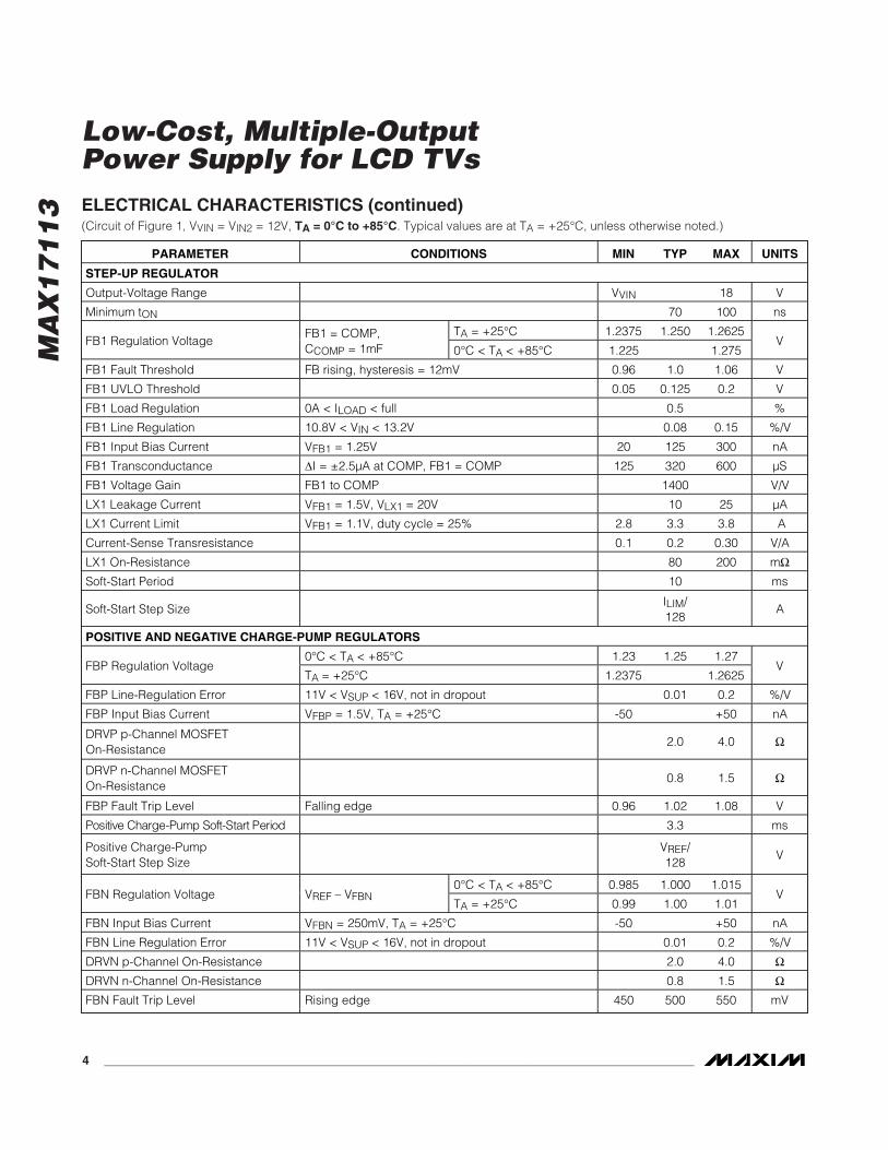
ELECTRICAL CHARACTERISTICS(Circuit of Figure 1, VVIN = VIN2 = 12V, TA = 0°C to +85°C. Typical values are at TA = +25°C, unless otherwise noted.)
Stresses beyond those listed under “Absolute Maximum Ratings” may cause permanent damage to the device. These are stress ratings only, and functionaloperation of the device at these or any other conditions beyond those indicated in the operational sections of the specifications is not implied. Exposure toabsolute maximum rating conditions for extended periods may affect device reliability.
VIN, IN2, EN1, EN2, FSEL to AGND.......................-0.3V to +24VCPGND, GND2, PGND to AGND........................................±0.3VMODE, DLP, CTL, THR, DEL1, DEL2, VL,
PGOOD to AGND .............................................-0.3V to +7.5VREF, FBP, FBN, FB1, FB2, COMP, OUT,
CRST to AGND .......................................-0.3V to (VVL + 0.3V)LX1, SWI, SWO to AGND .......................................-0.3V to +24VSWI to SWO............................................................-0.3V to +24VDRVN to AGND..........................................-0.3V to (VIN2 + 0.3V)DRVP to AGND ........................................-0.3V to (VSWO + 0.3V)LX2 to GND2..............................................-0.3V to (VIN2 + 0.3V)BST to VL................................................................-0.3V to +24VSRC to AGND.........................................................-0.3V to +48VGON, DRN to AGND.................................-0.3V to (VSRC + 0.3V)SRC to DRN............................................................-0.3V to +40VDRN to AGND.........................................................-0.3V to +40VGON to DRN...........................................................-0.3V to +48VREF Short Circuit to AGND.........................................Continuous
RMS LX1 Current (total for both pins) ...................................3.2ARMS PGND Current (total for both pins) ...............................3.2ARMS IN2 Current (total for both pins)....................................3.2ARMS LX2 Current (total for both pins) ...................................3.2ARMS GND2, CPGND Current................................................0.8ARMS SWI Current ..................................................................2.4ARMS SWO Current ................................................................2.4ARMS DRVN, DRVP Current ...................................................0.8ARMS VL Current ..................................................................50mAContinuous Power Dissipation (TA = +70°C)
40-Pin Thin QFN(derate 35.7mW/°C above +70°C) .........................2857.1mW
Operating Temperature Range ...........................-40°C to +85°CJunction Temperature ......................................................+160°CStorage Temperature Range .............................-65°C to +165°CLead Temperature (soldering, 10s)....................................+300°
PARAMETER CONDITIONS MIN TYP MAX UNITS
GENERAL
VIN, IN2 Input Voltage Range 8.5 16.5 V
VIN + IN2 Quiescent Current Only LX2 switching (VFB1 = VFBP = 1.5V, VFBN = 0V); EN1 = EN2 = VL, VFSEL= 0V
10 mA
VIN + IN2 Standby Current LX2 not switching (VFB1 = VFB2 = VFBP = 1.5V, VFBN = 0V); EN1 = EN2 = VL, VFSEL= 0V
3 mA
VIN + IN2 Shutdown Current EN1 = EN2 = AGND (shutdown) 300 600 μA
SWO Shutdown Current EN1 = EN2 = AGND (shutdown) 0.25 2 μA
FSEL = VIN 510 600 690 SMPS Operating Frequency
FSEL = AGND 390 450 510 kHz
Phase Difference Between Step-Down/Positive and Step-Up/Negative Regulators
180 Degrees
VIN Undervoltage Lockout Threshold VIN rising edge, 100mV typical hysteresis 6.0 7.0 8.3 V
VL REGULATOR
VL Output Voltage IVL = 25mA, VFB1 = VFB2 = VFBP = 1.1V, VFBN = 0.4V (all regulators switching)
4.9 5.0 5.15 V
VL Undervoltage Lockout Threshold VL rising edge, 100mV typical hysteresis 3.6 4.0 4.5 V

MA
X1
71
13
Low-Cost, Multiple-OutputPower Supply for LCD TVs
_______________________________________________________________________________________ 3
PARAMETER CONDITIONS MIN TYP MAX UNITS
REFERENCE
REF Output Voltage No external load 1.235 1.250 1.265 V
REF Load Regulation 0 < ILOAD < 50μA 10 mV
REF Sink Current In regulation 10 μA
RE F U nd er vol tag e- Lockout Thr eshol d Rising edge; 25mV typical hysteresis 1.0 1.2 V
STEP-DOWN REGULATOR
0°C < TA < +85°C 3.25 3.30 3.35OUT Voltage in Fixed Mode
FB2 = AGND, no load(Note 1) TA = +25°C 3.267 3.333
V
0°C < TA < +85°C 1.23 1.25 1.27FB2 Voltage in Adjustable Mode
VOUT = 2.5V, no load(Note 1) TA = +25°C 1.2375 1.2625
V
FB2 Adjustable-ModeThreshold Voltage
Dual-mode comparator 0.10 0.15 0.20 V
Output-Voltage Adjust Range Step-down output 1.5 5.0 V
FB2 Fault Trip Level Falling edge 0.94 1.00 1.06 V
FB2 Input Bias Current VFB2 = 1.5V, TA = +25°C 50 125 200 nA
DC Load Regulation 0.4A < ILOAD < 2A 0.5 %
DC Line Regulation No load, 10.8V < VIN2 < 13.2V 0.05 %/V
LX2-to-IN2 nMOS SwitchOn-Resistance
100 200 mΩ
LX2-to-CPGND nMOS SwitchOn-Resistance
7 12 25 Ω
BST-to-VL pMOS SwitchOn-Resistance
7 12 25 Ω
Low-Frequency OperationOUT Threshold
Step-down only 0.8 V
FSEL = VIN 100Low-Frequency OperationSwitching Frequency FSEL = AGND 75
kHz
LX2 Positive Current Limit 2.50 3 3.50 A
Soft-Start Period 3.3 ms
Soft-Start Step SizeVREF/128
V
Maximum Duty Factor 65 75 90 %
POWER-GOOD
FB2 Power-Good Threshold FB2 rising 0.94 1.00 1.06 V
FB2 Threshold Hysteresis 12 mV
PGOOD Output Low Voltage IPGOOD = 1mA 0.1 0.3 V
PGOOD Leakage Current VPGOOD = 3V, TA = +25°C 1 μA
CRST Charge Current VCRST = 1V 0.8 1.0 1.2 μA
CRST Voltage Threshold 1.2 1.25 1.3 V
CRST Pulldown Resistance VCRST = 1V 150 300 Ω
ELECTRICAL CHARACTERISTICS (continued)(Circuit of Figure 1, VVIN = VIN2 = 12V, TA = 0°C to +85°C. Typical values are at TA = +25°C, unless otherwise noted.)
MA
X1
71
13
Low-Cost, Multiple-OutputPower Supply for LCD TVs
4 _______________________________________________________________________________________
ELECTRICAL CHARACTERISTICS (continued)(Circuit of Figure 1, VVIN = VIN2 = 12V, TA = 0°C to +85°C. Typical values are at TA = +25°C, unless otherwise noted.)
PARAMETER CONDITIONS MIN TYP MAX UNITS
STEP-UP REGULATOR
Output-Voltage Range VVIN 18 V
Minimum tON 70 100 ns
TA = +25°C 1.2375 1.250 1.2625FB1 Regulation Voltage
FB1 = COMP,CCOMP = 1mF 0°C < TA < +85°C 1.225 1.275
V
FB1 Fault Threshold FB rising, hysteresis = 12mV 0.96 1.0 1.06 V
FB1 UVLO Threshold 0.05 0.125 0.2 V
FB1 Load Regulation 0A < ILOAD < full 0.5 %
FB1 Line Regulation 10.8V < VIN < 13.2V 0.08 0.15 %/V
FB1 Input Bias Current VFB1 = 1.25V 20 125 300 nA
FB1 Transconductance ΔI = ±2.5μA at COMP, FB1 = COMP 125 320 600 μS
FB1 Voltage Gain FB1 to COMP 1400 V/V
LX1 Leakage Current VFB1 = 1.5V, VLX1 = 20V 10 25 μA
LX1 Current Limit VFB1 = 1.1V, duty cycle = 25% 2.8 3.3 3.8 A
Current-Sense Transresistance 0.1 0.2 0.30 V/A
LX1 On-Resistance 80 200 mΩ Soft-Start Period 10 ms
Soft-Start Step SizeILIM/128
A
POSITIVE AND NEGATIVE CHARGE-PUMP REGULATORS
0°C < TA < +85°C 1.23 1.25 1.27FBP Regulation Voltage
TA = +25°C 1.2375 1.2625V
FBP Line-Regulation Error 11V < VSUP < 16V, not in dropout 0.01 0.2 %/V
FBP Input Bias Current VFBP = 1.5V, TA = +25°C -50 +50 nA
DRVP p-Channel MOSFETOn-Resistance
2.0 4.0 Ω
DRVP n-Channel MOSFETOn-Resistance
0.8 1.5 Ω
FBP Fault Trip Level Falling edge 0.96 1.02 1.08 V
P osi ti ve C har g e- P um p S oft- S tar t P er i od 3.3 ms
Positive Charge-Pump Soft-Start Step Size
VREF/128
V
0°C < TA < +85°C 0.985 1.000 1.015 FBN Regulation Voltage VREF – VFBN TA = +25°C 0.99 1.00 1.01V
FBN Input Bias Current VFBN = 250mV, TA = +25°C -50 +50 nA
FBN Line Regulation Error 11V < VSUP < 16V, not in dropout 0.01 0.2 %/V
DRVN p-Channel On-Resistance 2.0 4.0 Ω DRVN n-Channel On-Resistance 0.8 1.5 ΩFBN Fault Trip Level Rising edge 450 500 550 mV

MA
X1
71
13
Low-Cost, Multiple-OutputPower Supply for LCD TVs
_______________________________________________________________________________________ 5
ELECTRICAL CHARACTERISTICS (continued)(Circuit of Figure 1, VVIN = VIN2 = 12V, TA = 0°C to +85°C. Typical values are at TA = +25°C, unless otherwise noted.)
PARAMETER CONDITIONS MIN TYP MAX UNITS
Negative Charge-Pump Soft-Start Period
2 ms
Negative Charge-Pump Soft-Start Step Size
( V RE F - V FB N /128
V
AVDD SWITCH
SWI Supply Range 8.0 18.5 V
SWI Overvoltage Fault Threshold SWI rising edge, 300mV typical hysteresis (Note 2) 18.50 19.2 19.90 V
SWI-SWO Switch Resistance 120 250 mΩHIGH-VOLTAGE SWITCH ARRAY
SRC Supply Range 44 V
SRC Supply Current 250 500 μA
GON-to-SRC Switch On-Resistance VDLP = 2V, CTL = VL 10 20 ΩG ON - to- S RC S w i tch S atur ati on C ur r ent (VSRC - VGON) > 5V 180 390 mA
GON-to-DRN Switch On-Resistance VDLP = 2V, CTL = AGND 25 50 ΩGO N - to- D RN S w i tch S atur ati on C ur r ent (VGON - VDRN) > 5V 40 180 mA
GON-to-GND Switch On-Resistance DLP = AGND, VGON = 5V 5 10 kΩCTL Input Low Voltage 0.6 V
CTL Input High Voltage 1.6 V
CTL Input Current CTL = AGND or VL, TA = +25°C -1 +1 μA
C TL- to- G ON Ri si ng P r op ag ati on D el ay1kΩ fr om D RN to GN D , C TL = AGN D to V L step , nol oad on G ON , m easur ed fr om V C TL = 2V to GON = 20%
100 ns
C TL- to- GON Fal l i ng P r op ag ati on D el ay1kΩ fr om D RN to GN D , C TL = V L to AGN D step , no l oad on GON , m easur ed fr om V C TL = 0.6V to GON = 80%
200 ns
MODE Switch On-Resistance 1200 ΩMode 1 Voltage Threshold VMODE rising 3.8 4.1 V
MODE Capacitor Charge Current(Mode 2)
V M OD E = 1V 40 50 65 μA
M O D E V ol tag e Thr eshol d for E nab l i ng D RN S w i tch C ontr ol i n M od e 2
GON connects to DRN 1.15 1.25 1.35 V
MODE Current-Source StopVoltage Threshold
MODE rising 2 3 V
THR-to-GON Voltage Gain 9.4 10.0 10.6 V/V
SEQUENCE CONTROL
EN1, EN2 Input Low Voltage 0.6 V
EN1, EN2 Input High Voltage 1.6 V
EN1, EN2 Pulldown Resistance 1 MΩDEL1, DEL2, DLP Charge Current VDEL1 = VDEL2 = VDLP = 1V 7 8 9 μA
DEL1, DEL2, DLP Turn-On Threshold 1.2 1.25 1.32 kV
DEL1, DEL2, DLP DischargeSwitch On-Resistance
EN1 = AGND or fault tripped 10 Ω
FBN D i schar g e S w i tch On- Resi stance EN2 = AGND or fault tripped 3 kΩ

MA
X1
71
13
Low-Cost, Multiple-OutputPower Supply for LCD TVs
6 _______________________________________________________________________________________
ELECTRICAL CHARACTERISTICS (continued)(Circuit of Figure 1, VVIN = VIN2 = 12V, TA = 0°C to +85°C. Typical values are at TA = +25°C, unless otherwise noted.)
PARAMETER CONDITIONS MIN TYP MAX UNITS
FAULT DETECTION
Duration to Trigger Fault 45 55 65 ms
Duration to Restart After Fault 240 ms
Number of Restart Attempts Before Shutdown
3 Times
Thermal-Shutdown Threshold 15°C typical hysteresis +160 °C
SWITCHING FREQUENCY SELECTION
FSEL Input Low Voltage 450kHz 0.6 V
FSEL Input High Voltage 600kHz 1.6 V
FSEL Pulldown Resistance 1 M
ELECTRICAL CHARACTERISTICS(Circuit of Figure 1, VVIN = VIN2 = 12V, TA = -40°C to +85°C. Typical values are at TA = +25°C, unless otherwise noted.) (Note 3)
PARAMETER CONDITIONS MIN TYP MAX UNITS
GENERAL
VIN + IN2 Input-Voltage Range 8.5 16.5 V
VIN + IN2 Shutdown Current EN1 = EN2 = AGND (shutdown) 600 μA
SWO Shutdown Current EN1 = EN2 = AGND (shutdown) 2 μA
FSEL = VIN 510 690SMPS Operating Frequency
FSEL = AGND 390 510kHz
VIN Undervoltage-Lockout Threshold VIN rising edge, 100mV typical hysteresis 5.75 7.25 V
VL REGULATOR
VL Output VoltageIVL = 25mA, VFB1 = VFB2 = VFBP = 1.1V,VFBN = 0.4V (all regulators switching)
4.9 5.15 V
VL Undervoltage-Lockout Threshold VL rising edge, 100mV typical hysteresis 3.6 4.5 V
REFERENCE
REF Output Voltage No external load 1.235 1.265 V
REF Load Regulation 0 < ILOAD < 50μA 10 mV
RE F U nd er vol tag e- Lockout Thr eshol d Rising edge; 25mV typical hysteresis 1.2 V
STEP-DOWN REGULATOR
OUT Voltage in Fixed Mode FB2 = GND, no load (Note 1) 3.25 3.35 V
FB2 Voltage in Adjustable Mode VOUT = 2.5V, no load (Note 1) 1.23 1.27 V
FB2 Adjustable-ModeThreshold Voltage
Dual-mode comparator 0.10 0.20 V
Output-Voltage Adjust Range Step-down output 1.5 5.0 V

MA
X1
71
13
Low-Cost, Multiple-OutputPower Supply for LCD TVs
_______________________________________________________________________________________ 7
ELECTRICAL CHARACTERISTICS (continued)(Circuit of Figure 1, VVIN = VIN2 = 12V, TA = -40°C to +85°C. Typical values are at TA = +25°C, unless otherwise noted.) (Note 3)
PARAMETER CONDITIONS MIN TYP MAX UNITS
LX2-to-IN2 nMOS SwitchOn-Resistance
200 mΩ
LX2-to-CPGND nMOS SwitchOn-Resistance
7 25 Ω
BS T- to- V L p M O S S w i tch On- Resi stance 7 25 Ω
LX2 Positive Current Limit 2.50 3.50 A
Maximum Duty Factor 65 90 %
FB2 Power-Good Threshold FB2 rising 0.94 1.06 V PGOOD Output Low Voltage IPGOOD = 1mA 0.3 V CRST Charge Current VCRST = 1V 0.8 1.2 μA
CRST Voltage Threshold 1.2 1.3 V CRST Pulldown Resistance VCRST = 1V 300 ΩSTEP-UP REGULATOR
Output-Voltage Range VVIN 18 VOscillator Maximum Duty Cycle 65 90 %
FB1 Regulation Voltage FB1 = COMP, CCOMP = 1nF 1.225 1.275 V
LX1 Current Limit VFB1 = 1.1V, duty cycle = 25% 3.2 4.2 A
Current-Sense Transresistance 0.10 0.30 V/A
LX1 On-Resistance 200 mΩ
POSITIVE AND NEGATIVE CHARGE-PUMP REGULATORS
FBP Regulation Voltage 1.23 1.27 V
DRVP p-Channel MOSFETOn-Resistance
4 Ω
DRVP n-Channel MOSFETOn-Resistance
1.5 Ω
FBN Regulation Voltage VREF - VFBN 0.985 1.015 V
DRVN p-Channel On-Resistance 3 Ω
DRVN n-Channel On-Resistance 1.5 Ω
AVDD SWITCH
SWI Supply Range 8.0 18.5 V
SWI Overvoltage Fault Threshold VSWI = rising, 300mV typical hysteresis (Note 3) 18.5 19.9 V
SWI-SWO Switch Resistance 360 mΩ
HIGH-VOLTAGE SWITCH ARRAY
SRC Supply Range 44 V
GON-to-SRC Switch On-Resistance VDLP = 2V, CTL = VL 20 Ω
GON-to-DRN Switch On-Resistance VDLP = 2V, CTL = AGND 50 Ω
GON-to-GND Switch On-Resistance DLP = AGND, VGON = 5V 2.5 10 kΩ
CTL Input Low Voltage 0.6 V
CTL Input High Voltage 1.6 V
Mode 1 Voltage Threshold VMODE rising edge 4.1 V

MA
X1
71
13
Low-Cost, Multiple-OutputPower Supply for LCD TVs
8 _______________________________________________________________________________________
Note 1: When the inductor is in continuous conduction (EN2 = VL or heavy load), the output voltage has a DC regulation level lower thanthe error comparator threshold by 50% of the output-voltage ripple. In discontinuous conduction (EN2 = GND with light load), theoutput voltage has a DC regulation level higher than the error comparator threshold by 50% of the output-voltage ripple.
Note 2: Disables boost switching if either SUP, SWI, or OVIN exceeds the threshold. Switching resumes when no threshold is exceeded.Note 3: Specifications to TA = -40°C are guaranteed by design, not production tested.
ELECTRICAL CHARACTERISTICS (continued)(Circuit of Figure 1, VVIN = VIN2 = 12V, TA = -40°C to +85°C. Typical values are at TA = +25°C, unless otherwise noted.) (Note 3)
PARAMETER CONDITIONS MIN TYP MAX UNITS
MODE Voltage Threshold for Enabling DRN Switch Control in Mode 2
GON connects to DRN 1.15 1.35 V
MODE Current-Source Stop Voltage Threshold
MODE rising 2 3 V
THR-to-GON Voltage Gain 9.4 10.6 V/V
SEQUENCE CONTROL
EN1, EN2 Input Low Voltage 0.6 V
EN1, EN2 Input High Voltage 1.6 V
SWITCHING FREQUENCY SELECTION
FSEL Input Low Voltage 600kHz 0.6 V
FSEL Input High Voltage 1.2MHz 1.6 V
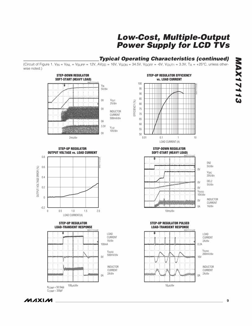
Typical Operating Characteristics(Circuit of Figure 1. VIN = VINL = VSUPP = 12V, AVDD = 16V, VGON = 34.5V, VGOFF = -6V, VOUT1 = 3.3V, TA = +25°C, unless other-wise noted.)
STEP-DOWN REGULATOR EFFICIENCYvs. LOAD CURRENT
LOAD CURRENT (A)
EFFI
CIE
NC
Y (%
)
10.10
55
60
65
70
75
80
85
500.01 10
MA
X17
113
toc0
1
EN1 = VL, EN2 = VL
EN1 = VL, EN2 = GND
STEP-DOWN REGULATOR OUTPUTVOLTAGE vs. LOAD CURRENT
LOAD CURRENT (A)
OU
TPU
T-VO
LTAG
E ER
ROR
(%)
2.001.601.200.800.40
-1
0
1
2
3
-20 2.40
MA
X17
113
toc0
2
EN2 = VL
EN2 = GND
STEP-DOWN REGULATOR LOAD-TRANSIENT RESPONSE
MAX17113 toc03
50mA
3.3V
0A
IOUT2A/div
VOUT200mV/divAC-COUPLED
INDUCTORCURRENT2A/div
20Fs/div
L = 4.7FH
MA
X1
71
13
Low-Cost, Multiple-OutputPower Supply for LCD TVs
_______________________________________________________________________________________ 9
Typical Operating Characteristics (continued)(Circuit of Figure 1. VIN = VINL = VSUPP = 12V, AVDD = 16V, VGON = 34.5V, VGOFF = -6V, VOUT1 = 3.3V, TA = +25°C, unless other-wise noted.)
STEP-DOWN REGULATOR SOFT-START (HEAVY LOAD)
MAX17113 toc04
0V
0V
0A
VIN5V/div
VOUT2V/div
3.3V
0V
VLX210V/div
INDUCTORCURRENT500mA/div
2ms/div
STEP-UP REGULATOR EFFICIENCY vs. LOAD CURRENT
LOAD CURRENT (A)
EFFI
CIE
NC
Y (%
)10.1
55
60
65
70
75
80
85
90
95
100
500.01 10
MA
X17
113
toc0
5
STEP-UP REGULATOR OUTPUT VOLTAGE vs. LOAD CURRENT
LOAD CURRENT(A)
OU
TPU
T-VO
LTAG
E ER
ROR
(%)
1.51.00.5
0
0.2
0.4
0.6
0.8
-0.20 2.0
MAX
1711
3 to
c06
STEP-DOWN REGULATOR SOFT-START (HEAVY LOAD)
MAX17113 toc07
0V
0V
0V
0V
0A
EN25V/div
VAVDD10V/div
INDUCTORCURRENT1A/div
DEL25V/div
VSRC20V/div
10ms/div
STEP-UP REGULATOR LOAD-TRANSIENT RESPONSE
MAX17113 toc08
0V
INDUCTORCURRENT2A/div
0A
LOADCURRENT1A/div
RCOMP = 50.5kICCOMP = 330pF
VAVDD500mV/div
100mA
100Fs/div
STEP-UP REGULATOR PULSED LOAD-TRANSIENT RESPONSE
MAX17113 toc09
16V
INDUCTORCURRENT2A/div
0A
LOADCURRENT2A/div
VAVDD200mV/div
0.2A
10Fs/div
MA
X1
71
13
Low-Cost, Multiple-OutputPower Supply for LCD TVs
10 ______________________________________________________________________________________
STEP-UP REGULATOR CURRENT LIMITvs. INPUT VOLTAGE
INPUT VOLTAGE (V)
STEP
-UP
REG
ULA
TOR
CU
RREN
T LI
MIT
(A)
131211109
3.0
3.5
4.0
2.58 14
MA
X17
113
toc1
0
L1 = 10FH
TIME-DELAY LATCHRESPONSE TO OVERLOAD
MAX17113 toc11
0V
0V
0A
VOUT5V/div
VAVDD10V/div
VGON50V/div
VGOFF50V/div
L2 INDUCTORCURRENT5A/div
0V
200ms/div
SWITCHING FREQUENCY vs. INPUT VOLTAGE
VIN (V)
SWIT
CH
ING
FRE
QU
ENC
Y (k
Hz)
131211109
592
594
596
598
600
602
604
606
608
610
5908 14
MA
X17
113
toc1
2
VL LOAD REGULATION
LOAD CURRENT (mA)
OU
TPU
T-VO
LTAG
E ER
ROR
(%)
80604020
-1
0
1
2
-20 100
MA
X17
113
toc1
3
NORMALIZED REFERENCE VOLTAGE LOAD REGULATION
LOAD CURRENT (FA)
OU
TPU
T-VO
LTAG
E ER
ROR
(%)
15010050
-0.1
0
0.1
0.2
-0.20 200
MA
X17
113
toc1
4
POSITIVE CHARGE-PUMP REGULATORNORMALIZED LINE REGULATION
VIN (V)
POSI
TIVE
CH
ARG
E-PU
MP
OU
TPU
T-VO
LTAG
E ER
ROR
17161514131211
-0.07
-0.04
-0.01
0.02
0.05
-0.1010 18
MA
X17
113
toc1
5
ISRC = 0A
ISRC = 25mA
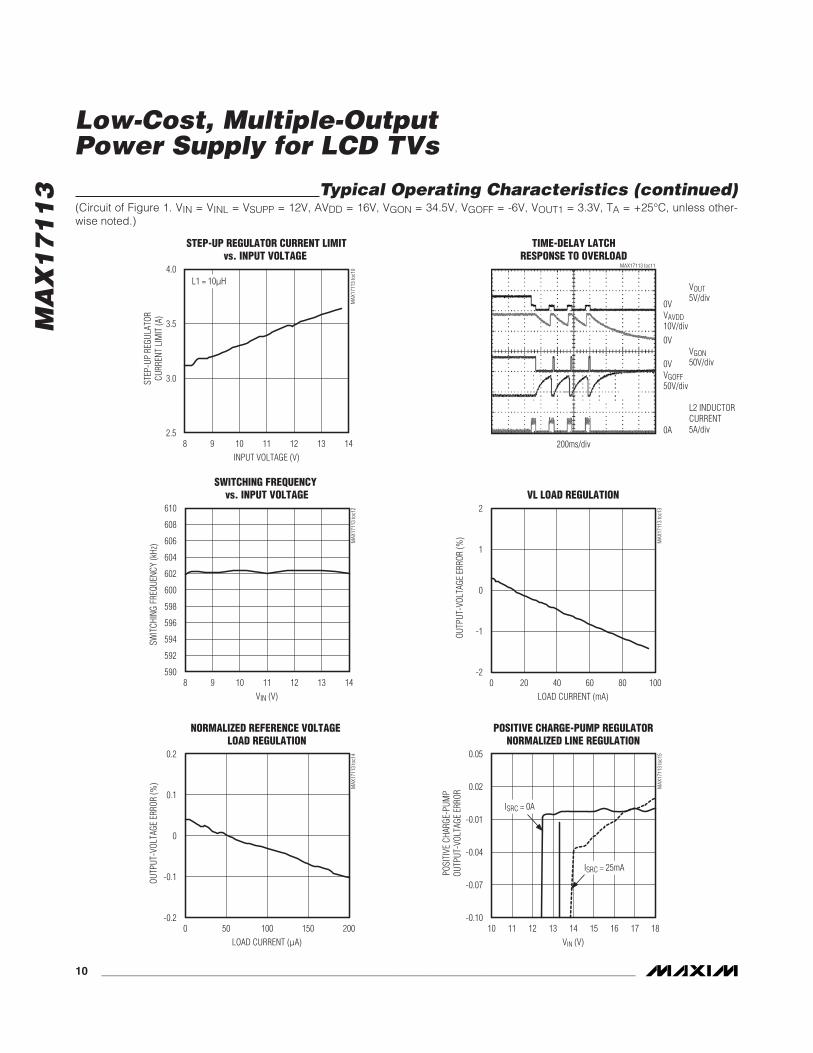
Typical Operating Characteristics (continued)(Circuit of Figure 1. VIN = VINL = VSUPP = 12V, AVDD = 16V, VGON = 34.5V, VGOFF = -6V, VOUT1 = 3.3V, TA = +25°C, unless other-wise noted.)

MA
X1
71
13
Low-Cost, Multiple-OutputPower Supply for LCD TVs
______________________________________________________________________________________ 11
Typical Operating Characteristics (continued)(Circuit of Figure 1. VIN = VINL = VSUPP = 12V, AVDD = 16V, VGON = 34.5V, VGOFF = -6V, VOUT1 = 3.3V, TA = +25°C, unless other-wise noted.)
POSITIVE CHARGE-PUMP REGULATORNORMALIZED LOAD REGULATION
LOAD CURRENT (mA)
OU
TPU
T-VO
LTAG
E ER
ROR
(%)
125100755025
-1.6
-1.2
-0.8
-0.4
0
0.4
0.8
-2.00 150
MA
X17
113
toc1
6
POSITIVE CHARGE-PUMP REGULATOR LOAD-TRANSIENT RESPONSE
MAX17113 toc17
70mA
10mA
VSRC500mV/div
LOADCURRENT20mA/div
34.8V
100Fs/div
NEGATIVE CHARGE-PUMP REGULATORNORMALIZED LINE REGULATION
VIN (V)
OU
TPU
T-VO
LTAG
E ER
ROR
(%)
151413121110
-0.55
-0.35
-0.15
0.05
0.25
-0.759 16
MA
X17
113
toc1
8
NEGATIVE CHARGE-PUMP REGULATORNORMALIZED LOAD REGULATION
LOAD CURRENT (mA)
OUTP
UT-V
OLTA
GE E
RROR
(%)
20015050 100
-1.0
-0.8
-0.6
-0.4
0
-0.2
0.2
0.4
-1.20 250
MA
X17
113
toc1
9
NEGATIVE CHARGE-PUMP REGULATOR LOAD-TRANSIENT RESPONSE
MAX17113 toc20
110mA
10mA
VGOFF200mV/div
LOADCURRENT50mA/div
-6V
100Fs/div
POWER-UP SEQUENCEMAX17113 toc21
0V
0V
0V
0V0V
0V
VEN15V/divVOUT5V/divVDEL15V/divVGOFF5V/divVAVDD10V/divVDEL25V/div
VSRC20V/div
20ms/div

MA
X1
71
13
Low-Cost, Multiple-OutputPower Supply for LCD TVs
12 ______________________________________________________________________________________
Typical Operating Characteristics (continued)(Circuit of Figure 1. VIN = VINL = VSUPP = 12V, AVDD = 16V, VGON = 34.5V, VGOFF = -6V, VOUT1 = 3.3V, TA = +25°C, unless other-wise noted.)
POWER-GOOD FUNCTIONMAX17113 toc22
0V
0V
0V
0V
VOUT1V/div
VCRST1V/div
VIN5V/div
VPGOOD5V/div
4ms/div
VIN SUPPLY CURRENT vs. VIN VOLTAGE
VIN VOLTAGE (V)VI
N S
UPP
LY C
URR
ENT
(mA)
161514131211109
1
2
3
4
5
6
08
MA
X17
113
toc2
3
EN1 = EN2 = VL
EN1 = EN2 = GND
603510-15-40 85
0.5
1.0
1.5
2.0
2.5
3.0
0
TEMPERATURE (NC)
VIN
SU
PPLY
CU
RREN
T (m
A)
VIN SUPPLY CURRENTvs. TEMPERATURE
MA
X17
113
toc2
4
EN1 = VL, EN2 = GND
EN1 = EN2 = GND
HIGH-VOLTAGE SWITCHCONTROL FUNCTION (MODE 1)
MAX17113 toc25
0V
0V
0V
VCTL5V/div
VMODE5V/div
VGON10V/div
4Fs/divRDRN = 1kICGON = 0.1FF
HIGH-VOLTAGE SWITCHCONTROL FUNCTION (MODE 2)
MAX17113 toc26
0V
0V
0V
VCTL5V/div
VMODE2V/div
VGON10V/div
4ms/divRDRN = 1kICGON = 0.1FF
MA
X1
71
13
Low-Cost, Multiple-OutputPower Supply for LCD TVs
______________________________________________________________________________________ 13
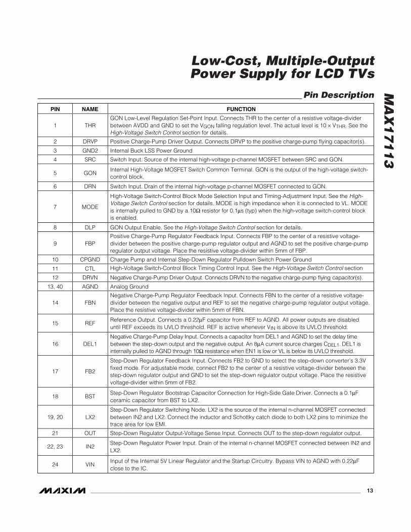
Pin DescriptionPIN NAME FUNCTION
1 THRGON Low-Level Regulation Set-Point Input. Connects THR to the center of a resistive voltage-dividerbetween AVDD and GND to set the VGON falling regulation level. The actual level is 10 × VTHR. See theHigh-Voltage Switch Control section for details.
2 DRVP Positive Charge-Pump Driver Output. Connects DRVP to the positive charge-pump flying capacitor(s).
3 GND2 Internal Buck LSS Power Ground
4 SRC Switch Input. Source of the internal high-voltage p-channel MOSFET between SRC and GON.
5 GONInternal High-Voltage MOSFET Switch Common Terminal. GON is the output of the high-voltage switch-control block.
6 DRN Switch Input. Drain of the internal high-voltage p-channel MOSFET connected to GON.
7 MODE
High-Voltage Switch-Control Block Mode Selection Input and Timing-Adjustment Input. See the High-Voltage Switch Control section for details. MODE is high impedance when it is connected to VL. MODEis internally pulled to GND by a 10Ω resistor for 0.1μs (typ) when the high-voltage switch-control blockis enabled.
8 DLP GON Output Enable. See the High-Voltage Switch Control section for details.
9 FBPPositive Charge-Pump Regulator Feedback Input. Connects FBP to the center of a resistive voltage-divider between the positive charge-pump regulator output and AGND to set the positive charge-pumpregulator output voltage. Place the resistive voltage-divider within 5mm of FBP.
10 CPGND Charge Pump and Internal Step-Down Regulator Pulldown Switch Power Ground
11 CTL High-Voltage Switch-Control Block Timing Control Input. See the High-Voltage Switch Control section
12 DRVN N eg ati ve C har g e- P um p D r i ver Outp ut. C onnects D RV N to the neg ati ve char g e- p um p fl yi ng cap aci tor ( s) .
13, 40 AGND Analog Ground
14 FBNNegative Charge-Pump Regulator Feedback Input. Connects FBN to the center of a resistive voltage-divider between the negative output and REF to set the negative charge-pump regulator output voltage.Place the resistive voltage-divider within 5mm of FBN.
15 REFReference Output. Connects a 0.22μF capacitor from REF to AGND. All power outputs are disableduntil REF exceeds its UVLO threshold. REF is active whenever VIN is above its UVLO threshold.
16 DEL1N eg ati ve C har g e- P um p D el ay Inp ut. C onnects a cap aci tor fr om D E L1 and AGN D to set the d el ay ti m eb etw een the step - d ow n outp ut and the neg ati ve outp ut. An 8μ A cur r ent sour ce char g es C D E L 1. D E L1 i si nter nal l y p ul l ed to AGN D thr oug h 10Ω r esi stance w hen E N 1 i s l ow or V L i s b el ow i ts U V LO thr eshol d .
17 FB2
Step-Down Regulator Feedback Input. Connects FB2 to GND to select the step-down converter’s 3.3Vfixed mode. For adjustable mode, connect FB2 to the center of a resistive voltage-divider between thestep-down regulator output and GND to set the step-down regulator output voltage. Place the resistivevoltage-divider within 5mm of FB2.
18 BSTStep-Down Regulator Bootstrap Capacitor Connection for High-Side Gate Driver. Connects a 0.1μFceramic capacitor from BST to LX2.
19, 20 LX2Step-Down Regulator Switching Node. LX2 is the source of the internal n-channel MOSFET connectedbetween IN2 and LX2. Connect the inductor and Schottky catch diode to both LX2 pins to minimize thetrace area for low EMI.
21 OUT Step-Down Regulator Output-Voltage Sense Input. Connects OUT to the step-down regulator output.
22, 23 IN2Step-Down Regulator Power Input. Drain of the internal n-channel MOSFET connected between IN2 andLX2.
24 VINInput of the Internal 5V Linear Regulator and the Startup Circuitry. Bypass VIN to AGND with 0.22μFclose to the IC.

MA
X1
71
13
Low-Cost, Multiple-OutputPower Supply for LCD TVs
14 ______________________________________________________________________________________
Pin Description (continued)
PIN NAME FUNCTION
25 FSEL Frequency Select Pin. Connect FSEL to AGND for 450kHz operation. Connect to VL or VIN for 600kHzoperation.
26 EN1 Step-Down and Negative Charge-Pump Regulator Enable Input. Input high also enables DLY1 pullup current.
27 DEL2
Step-Up Regulator and Positive Charge-Pump Delay Input. Connects a capacitor from DEL2 and AGND to set the delay time between EN2 and the startup of these regulators, or between the step-down startup and the startup of these regulators if EN1 is high before the step-down starts. An 8μA current source charges CDEL2. DEL2 is internally pulled to AGND through 10 resistance when EN1 or EN2 is low or when VL is below its UVLO threshold.
28 VL
5V Internal Linear Regulator Output. Bypass VL to AGND with 1 F minimum. Provides power for the internal MOSFET driving circuit, the PWM controllers, charge-pump regulators, logic, and reference and other analog circuitry. Provides 25mA load current when all switching regulators are enabled. VL is active whenever VIN is above its UVLO threshold.
29 EN2 Step-Up and Positive Charge-Pump Regulator Enable Input. Input high also enables DLY2 pullup current. EN2 is inactive when EN1 is low.
30, 31 PGND Step-Up Regulator Power Ground. Source of the internal power n-channel MOSFET.
32, 33 LX1 Step-Up Regulator Power MOSFET n-Channel Drain and Switching Node. Connects the inductor and Schottky catch diode to both LX1 pins and minimize the trace area for the lowest EMI.
34 SWI Step-Up Regulator Internal PMOS Pass Switch Source Input. Connects to the anode of the step-up regulator Schottky catch diode.
35 SWO Step-Up Regulator Internal pMOS Pass Switch Drain Output
36 FB1 Boost Regulator Feedback Input. Connects FB1 to the center of a resistive voltage-divider between the boost regulator output and AGND to set the boost regulator output voltage. Place the resistive voltage-divider within 5mm of FB1.
37 COMP Compensation Pin for the Step-Up Error Amplifier. Connects a series resistor and capacitor from COMP to AGND.
38 PGOOD Open-Drain Power-Good Output. Monitors the step-down output voltage.
39 CRST Power-Good Reset Timing Pin. Connects a capacitor from CRST to AGND to set the step-down output-rising PGOOD delay.
— EP Exposed Pad = AGND
MA
X1
71
13
Low-Cost, Multiple-OutputPower Supply for LCD TVs
______________________________________________________________________________________ 15
LX2
REF
FB1
LX1 LX1
AGND
COMP
VIN12V
OUT3.3V
2A
AVDD16V1.5A
FSEL
FB2
OUT
STEP-DOWN, NEGATIVEON/OFF
VL
VIN VIN
GON35V100mA
AGND
VL
REF
BST
GON
DRN
CTL FROM GONCONTROL
DRVN
FBN
REF
DRVP
FBPCPGND
SRC
PGND PGND
L14.7μH
10μF
L22.4μH
D2
D1
1μF
0.1μF
0.1μF
DEL2
DEL1
EN1
EN2
SWI
SWO
THR
DLP
MODE
C210μF
C310μF
30 31 32 33
34
35
36
37
40
1
11
1kΩ
6
5
PGOOD PGOOD38
CRST39
4
SRC
20.22μF
0.22μF 0.22μF
AVDD91014
12
IN2 IN2
2322
0.1μF
LX2
GND2
18
1920
3
21
17
24
2825
7
15
13
27
16
26
29
8
STEP-UP, POSITIVECHARGE PUMP ON/OFF
GOFF-6V
100mA
MAX17113
1μF
0.22μF
0.1μF
0.15μF
0.15μF
D3
D5
D4
C522μF
1μF
330pF100kΩ
33.3kΩ
2.2kΩ
3.3V
367kΩ
13.3kΩ
158kΩ
13.3kΩ
150kΩ
23kΩ
EP
C2410μF
C15, C162x10μF
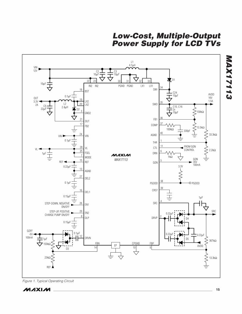
Figure 1. Typical Operating Circuit
MA
X1
71
13
Low-Cost, Multiple-OutputPower Supply for LCD TVs
16 ______________________________________________________________________________________
Typical Operating CircuitThe typical operating circuit (Figure 1) of theMAX17113 is a complete power-supply system for TFTLCD panels in monitors and TVs. The circuit generatesa +3.3V logic supply, a +16V source driver supply, a+34.5V positive gate driver supply, and a -6V negativegate driver supply from a 12V ±10% input supply.Table 1 lists some selected components and Table 2lists the contact information for component suppliers.
Detailed DescriptionThe MAX17113 is a multiple-output power supplydesigned primarily for TFT LCD panels used in monitorsand TVs. It contains a step-down switching regulator togenerate the logic supply rail, a step-up switching regu-lator to generate the source driver supply, and twocharge-pump regulators to generate the gate driversupplies. Each regulator features adjustable output volt-age, digital soft-start, and timer-delayed fault protection.Both the step-down and step-up regulators use a fixed-frequency current-mode control architecture. The twoswitching regulators are 180° out-of-phase to minimizethe input ripple. The internal oscillator offers two pin-selectable frequency options (450kHz/600kHz), allowingusers to optimize their designs based on the specificapplication requirements. In addition, the MAX17113features a high-voltage switch-control block, a PGOODlogic block, an internal 5V linear regulator, a 1.25V refer-ence output, well-defined power-up and power-downsequences, and thermal-overload protection. Figure 2shows the MAX17113 functional diagram.
Step-Down RegulatorThe step-down regulator consists of an internal n-chan-nel MOSFET with gate driver, a lossless current-sensenetwork, a current-limit comparator, and a PWM con-troller block. The external power stage consists of aSchottky diode rectifier, an inductor, and output capac-itors. The output voltage is regulated by changing theduty cycle of the n-channel MOSFET. A bootstrap cir-cuit that uses a 0.1μF flying capacitor between LX2 andBST provides the supply voltage for the high-side gatedriver. Although the MAX17113 also includes a 10Ω(typ) low-side MOSFET, this switch is used to chargethe bootstrap capacitor during startup and maintainsfixed-frequency operation at light load and cannot beused as a synchronous rectifier. An external Schottkydiode (D2 in Figure 1) is always required.
Table 1. Component ListDESIGNATION DESCRIPTION
C1, C2, C3
10μF ±20%, 16V X5R ceramic capacitors (1206) Taiyo Yuden EMK325BJ106MD TDK C3225X7R1C106M
C5
22μF ±10%, 6.3V X5R ceramic capacitor (1206) Taiyo Yuden JMK316BJ226KL Murata GRM31CR60J226M
C15, C16, C24 10μF ±20%, 25V X5R ceramic capacitors (1210) TDK C3225X5R1E106M
D1, D2 3A, 30V Schottky diodes (M-Flat) Toshiba CMS02 (TE12L,Q) Central Semiconductor
D3, D4, D5
200mA, 100V dual ultra-fast diodes (SOT23) Fairchild MMBD4148SE (top mark D4) Central Semiconductor CMPD1001S lead free (top mark L21)
L1Low-profile 4.7μH, 3.5A inductor (2mm height) TOKO FDV0620-4R7M
L2
Low-profile 2.4μH, 2.6A inductor (1.8mm height) TOKO 1124BS-2R4M (2.4μH) Würth 744052002 (2.5μH)
Table 2. Component SuppliersSUPPLIER PHONE FAX WEBSITE
Fairchild Semiconductor 408-822-2000 408-822-2102 www.fairchildsemi.com
Sumida Corp. 847-545-6700 847-545-6720 www.sumida.com
TDK Corp. 847-803-6100 847-390-4405 www.component.tdk.com
Toshiba America Electronic Components, Inc. 949-455-2000 949-859-3963 www.toshiba.com/taec

MA
X1
71
13
Low-Cost, Multiple-OutputPower Supply for LCD TVs
______________________________________________________________________________________ 17
STEP-DOWN OSC
VL
LX2
GND2
OUT
FB2
VIN
REF
AGND
DEL1
VL VL
VIN
VIN (12V)
3.3V2A
150mV
STEP-UP
POWER-UPSEQUENCE
HVSWITCHBLOCK
NEGATIVEREG
POSITIVEREG
IN2
LX1
PGND
FB1
COMP
FSEL
AGND
SWI
SWO
PGOOD PGOOD
3.3V
VL
BST
VGOFF-6V
100mA
REF
VL
AVDD16V1.5A
REF
DEL2DLP
DRVN
FBN FBP
REF
VIN
CPGND
50% OSC
EN1STEP-DOWN, NEGATIVEON/OFF
EN2STEP-UP, POSITIVECHARGE PUMP ON/OFF
P
VGON35V50mA
DRN
THR
MODE
CRST
CTL GONCONTROL
GON
AVDD
SRCSWO
SRCDRVP
CPGND
RESET
MAX17113
Figure 2. Functional Diagram
PWM Controller BlockThe heart of the PWM control block is a multi-input,open-loop comparator that sums three signals: the out-put-voltage signal with respect to the reference voltage,the current-sense signal, and the slope compensation.The PWM controller is a direct-summing type, lacking atraditional error amplifier and the phase shift associatedwith it. This direct-summing configuration approachesideal cycle-by-cycle control over the output voltage.
When EN1 and EN2 are high, the controller alwaysoperates in fixed-frequency PWM mode. Each pulsefrom the oscillator sets the main PWM latch that turnson the high-side switch until the PWM comparatorchanges state.
When EN1 is high and EN2 is low, the controller oper-ates in skip mode. The skip mode dramaticallyimproves light-load efficiency by reducing the effectivefrequency, which reduces switching losses. It keepsthe peak inductor current at about 0.9A (typ) in anactive cycle, al lowing subsequent cycles to beskipped. Skip mode transitions seamlessly to fixed-frequency PWM operation as load current increases.
Current Limiting and Lossless Current SensingThe current-limit circuit turns off the high-side MOSFETswitch whenever the voltage across the high-side MOSFET exceeds an internal threshold. The actual current limit is 3A (typ).
For current-mode control, an internal lossless sensenetwork derives a current-sense signal from the induc-tor DCR. The time constant of the current-sense net-work is not required to match the time constant of theinductor and has been chosen to provide sufficient cur-rent ramp signal for stable operation at both operatingfrequencies. The current-sense signal is AC-coupledinto the PWM comparator, eliminating most DC output-voltage variation with load current.
Low-Frequency OperationThe step-down regulator of the MAX17113 enters intolow-frequency operating mode if the voltage on OUT isbelow 0.8V. In the low-frequency mode, the switchingfrequency of the step-down regulator is 1/6 the oscilla-tor frequency. This feature prevents potentially uncon-trolled inductor current if OUT is overloaded or shortedto ground.
Dual-Mode FeedbackThe step-down regulator of the MAX17113 supportsboth fixed and adjustable output voltages. ConnectFB2 to AGND to enable the 3.3V fixed output voltage.Connect a resistive voltage-divider between OUT and
AGND with the center tap connected to FB2 to adjustthe output voltage. Choose RB (resistance from FB2 toAGND) to be between 5kΩ and 50kΩ, and solve for RA(resistance from OUT1 to FB1) using the equation:
where VFB2 = 1.25V, and VOUT can vary from 1.25V to 5V.
Because of FB2’s (pin 17) close proximity to the noisyBST (pin 18), a noise f i l ter is required for FB2adjustable-mode operation. Place a 100pF capacitorfrom FB2 to AGND to prevent unstable operation. No fil-ter is required for 3.3V fixed-mode operation.
Soft-StartThe step-down regulator includes a 7-bit soft-start DACthat steps its internal reference voltage from 0 to 1.25V in128 steps. The soft-start period is 3ms (typ) and FB2 faultdetection is disabled during this period. The soft-start fea-ture effectively limits the inrush current during startup (seethe Step-Down Regulator Soft-Start (Heavy Load) wave-forms in the Typical Operating Characteristics).
Step-Up RegulatorThe step-up regulator employs a current-mode, fixed-frequency PWM architecture to maximize loop band-width and provide fast-transient response to pulsedloads typical of TFT LCD panel source drivers. The inte-grated MOSFET and the built-in digital soft-start func-tion reduce the number of external componentsrequired while controlling inrush currents. The outputvoltage can be set from VIN to 20V with an externalresistive voltage-divider. The regulator controls the out-put voltage and the power delivered to the output bymodulating the duty cycle (D) of the internal powerMOSFET in each switching cycle. The duty cycle of theMOSFET is approximated by:
where VAVDD is the output voltage of the step-up regulator.
PWM Controller BlockAn error amplifier compares the signal at FB1 to 1.25Vand changes the COMP output. The voltage at COMPsets the peak inductor current. As the load varies, theerror amplifier sources or sinks current to the COMPoutput accordingly to produce the inductor peak cur-rent necessary to service the load. To maintain stabilityat high duty cycles, a slope compensation signal issummed with the current-sense signal.
DV V
VAVDD IN
AVDD≈
-
RA RBVVOUT
FB= ×
⎛⎝⎜
⎞⎠⎟2
1-
MA
X1
71
13
Low-Cost, Multiple-OutputPower Supply for LCD TVs
18 ______________________________________________________________________________________

MA
X1
71
13
Low-Cost, Multiple-OutputPower Supply for LCD TVs
______________________________________________________________________________________ 19
On the rising edge of the internal clock, the controllersets a flip-flop, turning on the n-channel MOSFET andapplying the input voltage across the inductor. The cur-rent through the inductor ramps up linearly, storing energy in its magnetic field. Once the sum of the current-feedback signal and the slope compensation exceed theCOMP voltage, the controller resets the flip-flop and turnsoff the MOSFET. Since the inductor current is continuous,a transverse potential develops across the inductor thatturns on the diode (D1). The voltage across the inductorthen becomes the difference between the output voltageand the input voltage. This discharge condition forcesthe current through the inductor to ramp back down,transferring the energy stored in the magnetic field to theoutput capacitor and the load. The MOSFET remains offfor the rest of the clock cycle.
Step-Up Regulator Internalp-Channel MOSFET Pass Switch
The MAX17113 includes an integrated 130mΩ high-voltage p-channel MOSFET to allow true shutdown ofthe step-up converter output (AVDD). This switch is typ-ically connected in series between the step-up regula-tor’s Schottky catch diode and its output capacitors. Inaddition to allowing step-up output to discharge com-pletely when disabled, this switch also controls thestartup inrush current into the step-up regulator’s out-put capacitors.
Soft-Start The step-up regulator includes a 7-bit soft-start DACthat steps its internal reference voltage from 0 to 1.25V
in 128 steps. This DAC also controls linearly the gate ofthe pMOS switch, which is in between SWI and SWO,and the output AVDD goes up smoothly, and when theAVDD reaches the input voltage, the step-up regulatortakes over seamlessly and the output-voltage AVDDreaches its regulation point. The soft-start period is10ms (typ) and FB1 fault detection is disabled duringthis period. The soft-start feature effectively limits theinrush current during startup.
Positive Charge-Pump RegulatorThe positive charge-pump regulator is typically used togenerate the positive supply rail for the TFT LCD gate driver ICs. The output voltage is set with an externalresistive voltage-divider from its output to GND with themidpoint connected to FBP. The number of charge-pump stages and the setting of the feedback dividerdetermine the output voltage of the positive charge-pump regulator. The charge pump includes a high-sidep-channel MOSFET (P1) and a low-side n-channelMOSFET (N1) to control the power transfer as shown inFigure 3.
During the first half-cycle, N1 turns on and charges fly-ing capacitors C20 and C21 (Figure 3). During the sec-ond half cycle, N1 turns off and P1 turns on, levelshifting C20 and C21 by VAVDD volts. If the voltageacross C23 plus a diode drop (VOUT + VD) is smallerthan the level-shifted flying capacitor voltage (VC20 +VAVDD), charge flows from C20 to C23 until the diode(D5) turns off. The amount of charge transferred to theoutput is determined by the error amplifier that controlsN1’s on-resistance.
REF1.25V
OSC
ERRORAMPLIFIER
P1
N1
DRVP
C22
D5
C23
C20
C21
CPGND
SWO
FBPPOSITIVE CHARGE-PUMP REGULATOR
AVDD
OUTPUT
MAX17113
Figure 3. Positive Charge-Pump Regulator Block Diagram

The positive charge-pump regulator’s startup can bedelayed by connecting an external capacitor fromDEL2 to AGND. An internal constant-current sourcebegins charging the DEL2 capacitor when EN2 is logic-high, and the step-down regulator reaches regulation.When the DEL2 voltage exceeds VREF, the positivecharge-pump regulator is enabled. Each time it isenabled, the positive charge-pump regulator goesthrough a soft-start routine by ramping up its internalreference voltage from 0 to 1.25V in 128 steps. Thesoft-start period is 3ms (typ) and FBP fault detection isdisabled during this period. The soft-start feature effec-tively limits the inrush current during startup.
Negative Charge-Pump RegulatorThe negative charge-pump regulator is typically used togenerate the negative supply rail for the TFT LCD gatedriver ICs. The output voltage is set with an external resis-tive voltage-divider from its output to REF with the mid-point connected to FBN. The number of charge-pumpstages and the setting of the feedback divider determinethe output of the negative charge-pump regulator. Thecharge-pump controller includes a high-side p-channelMOSFET (P2) and a low-side n-channel MOSFET (N2) tocontrol the power transfer as shown in Figure 4.
During the first half cycle, P2 turns on, and flyingcapacitor C13 charges to VIN minus a diode drop(Figure 4). During the second half cycle, P2 turns off,and N2 turns on, level shifting C13. This connects C13in parallel with reservoir capacitor C12. If the voltageacross C12 minus a diode drop is greater than the volt-age across C13, charge flows from C12 to C13 until thediode (D3) turns off. The amount of charge transferredfrom the output is determined by the error amplifier,which controls N2’s on-resistance.
The negative charge-pump regulator is enabled whenEN1 is logic-high and the step-down regulator reachesregulation. Each time it is enabled, the negativecharge-pump regulator goes through a soft-start rou-tine by ramping down its internal reference voltagefrom 1.25V to 250mV in 102 steps. The soft-start periodis 3ms (typ) and FBN fault detection is disabled duringthis period. The soft-start feature effectively limits theinrush current during startup.
MA
X1
71
13
Low-Cost, Multiple-OutputPower Supply for LCD TVs
20 ______________________________________________________________________________________
P2
N2
DRVN
CPGND
VIN
FBNNEGATIVE CHARGE-PUMP REGULATOR
OUTPUT
REF
MAX17113
C12
C13
R2
R1
D3
REF0.25V
OSC
ERRORAMPLIFIER
Figure 4. Negative Charge-Pump Regulator Block Diagram
MA
X1
71
13
Low-Cost, Multiple-OutputPower Supply for LCD TVs
______________________________________________________________________________________ 21
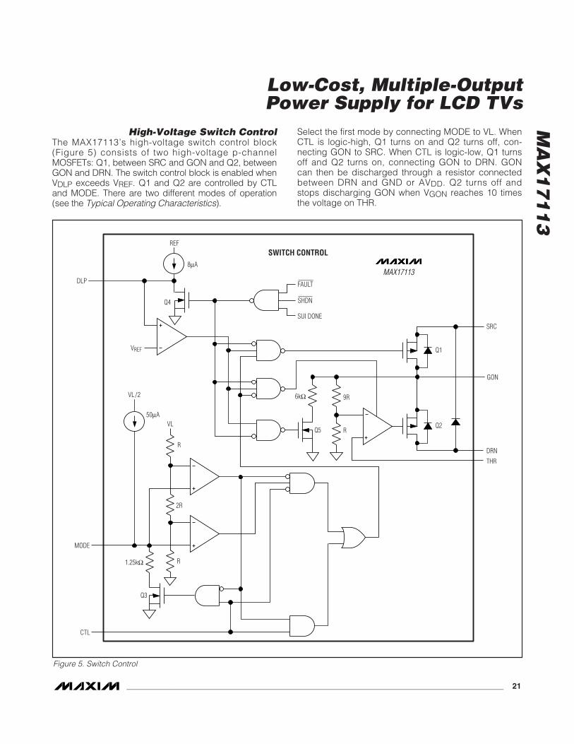
High-Voltage Switch ControlThe MAX17113’s high-voltage switch control block(Figure 5) consists of two high-voltage p-channelMOSFETs: Q1, between SRC and GON and Q2, betweenGON and DRN. The switch control block is enabled whenVDLP exceeds VREF. Q1 and Q2 are controlled by CTLand MODE. There are two different modes of operation(see the Typical Operating Characteristics).
Select the first mode by connecting MODE to VL. WhenCTL is logic-high, Q1 turns on and Q2 turns off, con-necting GON to SRC. When CTL is logic-low, Q1 turnsoff and Q2 turns on, connecting GON to DRN. GONcan then be discharged through a resistor connectedbetween DRN and GND or AVDD. Q2 turns off andstops discharging GON when VGON reaches 10 timesthe voltage on THR.
MODE
CTL
DLP
SRC
GON
DRN
VREF
SUI DONE
8μA
REF
Q1
Q4
Q3
R
2R
R
50μA
SWITCH CONTROL
THR
9R
RVL
VL /2
1.25kΩ
SHDN
FAULT
Q5
MAX17113
6kΩ
Q2
Figure 5. Switch Control
When VMODE is less than 0.8 x VVL, the switch controlblock works in the second mode. The rising edge ofVCTL turns on Q1 and turns off Q2, connecting GON toSRC. An internal n-channel MOSFET, Q3, betweenMODE and AGND is also turned on to discharge anexternal capacitor between MODE and AGND. Thefalling edge of VCTL turns off Q3, and an internal 50μAcurrent source starts charging the MODE capacitor.Once VMODE exceeds VVL/4, the switch control blockturns off Q1 and turns on Q2, connecting GON to DRN.GON can then be discharged through a resisor con-nected between DRN and PGND or AVDD. Q2 turns offand stops discharging GON when VGON reaches 10times the voltage on THR.
The switch control block is disabled and DLP is heldlow when EN1 or EN2 is low or the IC is in a fault state.
Linear Regulator (VL)The MAX17113 includes an internal linear regulator. VINis the input of the linear regulator. The input voltagerange is between 8V and 16.5V. The output voltage is setto 5V. The regulator powers the internal MOSFET drivers,PWM controllers, charge-pump regulators, and logic cir-cuitry. The total external load capability is 25mA. BypassVL to AGND with a minimum 1μF ceramic capacitor.
Reference Voltage (REF)The reference output is nominally 1.25V, and cansource at least 50μA (see the Typical OperatingCharacteristics). VL is the input of the internal referenceblock. Bypass REF with a 0.22μF ceramic capacitorconnected between REF and AGND.
Frequency Selection (FSEL)The step-down regulator and step-up regulator use thesame internal oscillator. The FSEL input selects theswitching frequency. Table 3 shows the switching fre-quency based on the FSEL connection. High-frequency(600kHz) operation optimizes the application for thesmallest component size, trading off efficiency due tohigher switching losses. Low-frequency (450kHz) oper-ation offers the best overall efficiency at the expense ofcomponent size and board space.
Power-Up SequenceThe step-down regulator starts up when the MAX17113’sinternal reference voltage (REF) is above its undervolt-age lockout (UVLO) threshold and EN1 is logic-high.
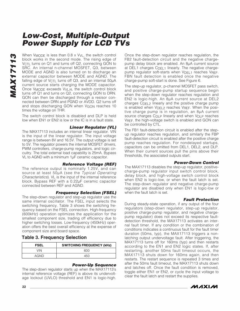
Once the step-down regulator reaches regulation, theFB2 fault-detection circuit and the negative charge-pump delay block are enabled. An 8μA current sourceat DEL1 charges CDEL1 linearly. The negative charge-pump regulator soft-starts when VDEL1 reaches VREF.FBN fault detection is enabled once the negativecharge-pump soft-start is done. See Figure 6.
The step-up regulator, p-channel MOSFET pass switch,and positive charge-pump startup sequence beginwhen the step-down regulator reaches regulation andEN2 is logic-high. An 8μA current source at DEL2charges CDEL2 linearly and the positive charge pumpis enabled when VDEL2 reaches VREF. When the posi-tive charge pump is in regulation, an 8μA currentsource charges CDLP linearly and when VDLP reachesVREF, the high-voltage switch is enabled and GON canbe controlled by CTL.
The FB1 fault-detection circuit is enabled after the step-up regulator reaches regulation, and similarly the FBPfault-detection circuit is enabled after the positive chargepump reaches regulation. For nondelayed startups,capacitors can be omitted from DEL1, DEL2, and DLP.When their current sources pull the pins above theirthresholds, the associated outputs start.
Power-Down ControlThe MAX17113 disables the step-up regulator, positive-charge-pump regulator input switch control block,delay block, and high-voltage switch control blockwhen EN2 is logic-low, or when the fault latch is set.The step-down regulator and negative charge-pumpregulator are disabled only when EN1 is logic-low orwhen the fault latch is set.
Fault ProtectionDuring steady-state operation, if any output of the fourregulators (step-down regulator, step-up regulator,positive charge-pump regulator, and negative charge-pump regulator) does not exceed its respective fault-detection threshold, the MAX17113 activates an inter-nal fault timer. If any condition or the combination ofconditions indicates a continuous fault for the fault timerduration (50ms, typ), the MAX17113 triggers a non-latching output undervoltage fault. After triggering, theMAX17113 turns off for 160ms (typ) and then restartsaccording to the EN1 and EN2 logic states. If, afterrestarting, another 50ms fault timeout occurs, theMAX17113 shuts down for 160ms again, and thenrestarts. The restart sequence is repeated 3 times andafter the 50ms fault timeout, the MAX17113 shuts downand latches off. Once the fault condition is removed,toggle either EN1 or EN2, or cycle the input voltage toclear the fault latch and restart the supplies.
MA
X1
71
13
Low-Cost, Multiple-OutputPower Supply for LCD TVs
22 ______________________________________________________________________________________
Table 3. Frequency Selection
FSEL SWITCHING FREQUENCY (kHz)
VIN 600
AGND 450
MA
X1
71
13
Low-Cost, Multiple-OutputPower Supply for LCD TVs
______________________________________________________________________________________ 23
DLP
TIME
TIME
VL/REF
VIN
NEGATIVE CHARGE-PUMPREGULATOR OUTPUT
POSITIVE CHARGE-PUMPREGULATOR OUTPUT
EN1 HIGH, REF, AND VL OKAY. START BUCK THEN DEL1 AFTER BUCK SS.
TIME
BUCK OUTPUT
DEL1 ABOVE REF. START NEGATIVE-CHARGE PUMP.
EN1
BUCK SS DONE AND EN2 HIGH. START SUI/BOOST AND CHARGE DEL2.
VINUVLO
VIN > UVLO. START VL AND REF.
AVDD
REF
DEL1
REF
TIME
GON DEPENDS ON CTL
EN2
REF
DEL2
GON
TIME
DLP ABOVE REF. STARTHIGH-VOLTAGE SWITCH BLOCK.
DEL2 ABOVE REF. START POSITIVE CP AND DLP.
SUI (INTERNAL SIGNAL)
BOOSTSWITCHING
SWOTURN-ON
SWO TURNS ON AND DEL2 CHARGES WHEN EN2 IS HIGH AND BUCK SS IS DONE.
VIN
tSS
tSS
tSStSS(BOOST)
GON CONNECTED TO GROUND
Figure 6. Startup Sequence

MA
X1
71
13
Low-Cost, Multiple-OutputPower Supply for LCD TVs
24 ______________________________________________________________________________________
Thermal-Overload ProtectionThe thermal-overload protection prevents excessivepower dissipation from overheating the MAX17113.When the junction temperature exceeds TJ = +160°C, athermal sensor immediately activates the fault protec-tion that shuts down all the outputs except the refer-ence and latches off, allowing the device to cool down.Once the device cools down by at least approximately15°C, cycle the input voltage to clear the fault latch andrestart the MAX17113.
The thermal-overload protection protects the controllerin the event of fault conditions. For continuous opera-tion, do not exceed the absolute maximum junctiontemperature rating of TJ = +150°C.
Design ProcedureStep-Down Regulator
Inductor SelectionThree key inductor parameters must be specified:inductance value (L), peak current (IPEAK), and DCresistance (RDC). The following equation includes aconstant, LIR, which is the ratio of peak-to-peak induc-tor ripple current to DC load current. A higher LIR valueallows smaller inductance, but results in higher lossesand higher ripple. A good compromise between sizeand losses is typically found at about 20% to 50% rip-ple-current to load-current ratio (LIR):
where IOUT(MAX) is the maximum DC load current, andthe switching frequency fSW is 600kHz when FSEL isconnected to VL or 450kHz when FSEL is connected toAGND. The exact inductor value is not critical and canbe adjusted to make trade-offs among size, cost, andefficiency. Lower inductor values minimize size andcost, but they also increase the output ripple andreduce the efficiency due to higher peak currents. Onthe other hand, higher inductor values increase effi-ciency, but at some point resistive losses due to extraturns of wire exceed the benefit gained from lower ACcurrent levels.
The inductor’s saturation current must exceed the peakinductor current. The peak current can be calculated by:
The inductor’s DC resistance should be low for goodefficiency. Find a low-loss inductor having the lowestpossible DC resistance that fits in the allotted dimen-sions. Ferrite cores are often the best choice. Shielded-core geometries help keep noise, EMI, and switchingwaveform jitter low.
Considering the typical operating circuit in Figure 1, themaximum load current (IOUT(MAX)) is 2A with a 3.3Voutput and a typical 12V input voltage. Choosing anLIR of 0.4 at this operating point:
At that operating point, the ripple current and the peakcurrent are:
Input CapacitorsThe input filter capacitors reduce peak currents drawnfrom the power source and reduce noise and voltageripple on the input caused by the regulator’s switching.They are usually selected according to input ripple cur-rent requirements and voltage rating, rather thancapacitance value. The input voltage and load currentdetermine the RMS input ripple current (IRMS):
The worst case is IRMS = 0.5 x IOUT, which occurs atVIN2 = 2 x VOUT.
For most applications, ceramic capacitors are usedbecause of their high ripple current and surge currentcapabilities. For optimal circuit long-term reliability,choose an input capacitor that exhibits less than +10°Ctemperature rise at the RMS input current correspondingto the maximum load current.
Output Capacitor SelectionSince the MAX17113’s step-down regulator is internallycompensated, it is stable with any reasonable amountof output capacitance. However, the actual capacitanceand equivalent series resistance (ESR) affect the regu-lator’s output ripple voltage and transient response. Therest of this section deals with how to determine the out-put capacitance and ESR needs according to the ripple-voltage and load-transient requirements.
I IV V V
VRMS OUTOUT IN OUT
IN= ×
× ( )2
2
-
I AA
AOUT PEAK_.
.= + =20 8
22 4
IV V VkHz μHOUT RIPPLE_
. ..
=× ( )
× ×≈
3 3 12 3 3600 5 0 12
-00 8. A
LV V V
V kHz AμHOUT =
× ( )× × ×
≈3 3 12 3 3
12 600 2 0 45 0
. ..
.-
I II
OUT PEAK OUT MAXOUT RIPPLE
_ ( )_= +2
IV V V
f L VOUT RIPPLEOUT IN OUT
SW OUT IN_ =
× ( )× ×
2
2
-
LV V V
V f I LIROUTOUT IN OUT
IN SW OUT MAX=
× ( )× × ×
2
2
-
( )
MA
X1
71
13
Low-Cost, Multiple-OutputPower Supply for LCD TVs
______________________________________________________________________________________ 25
The output-voltage ripple has two components: varia-tions in the charge stored in the output capacitor, andthe voltage drop across the capacitor’s ESR caused bythe current into and out of the capacitor:
where IOUT_RIPPLE is defined in the Inductor Selectionof the Step-Down Regulator section, COUT is the outputcapacitance, and RESR_OUT is the ESR of the outputcapacitor COUT. In Figure 1’s circuit, the inductor ripplecurrent is 0.8A. If the voltage-ripple requirement ofFigure 1’s circuit is ±1% of the 3.3V output, then thetotal peak-to-peak ripple voltage should be less than66mV. Assuming that the ESR ripple and the capacitiveripple each should be less than 50% of the total peak-to-peak ripple, then the ESR should be less than 43mΩand the output capacitance should be more than 5μF tomeet the total ripple requirement. A 22μF capacitor withESR (including PCB trace resistance) of 10mΩ is select-ed for the standard application circuit in Figure 1, whicheasily meets the voltage-ripple requirement.
The step-down regulator’s output capacitor and ESR canalso affect the voltage undershoot and overshoot whenthe load steps up and down abruptly. The step-downregulator’s transient response is typically dominated byits loop response and the time constant of its internalintegrator. However, excessive inductance or insufficientoutput capacitance can degrade the natural transientresponse. Calculating the ideal transient response ofthe inductor and capacitor, which assumes an idealresponse from the regulator, can ensure that thesecomponents do not degrade the IC’s natural response.
The ideal undershoot and overshoot have two compo-nents: the voltage steps caused by ESR, and the voltagesag and soar due to the finite capacitance and the induc-tor current slew rate. Use the following formulas to checkif the ESR is low enough and the output capacitance islarge enough to prevent excessive soar and sag.
The amplitude of the ESR step is a function of the loadstep and the ESR of the output capacitor:
The amplitude of the capacitive sag is a function of theload step, the output capacitor value, the inductorvalue, the input-to-output voltage differential, and themaximum duty cycle:
The amplitude of the capacitive soar is a function of theload step, the output capacitor value, the inductorvalue, and the output voltage:
Keeping the full-load overshoot and undershoot lessthan 3% ensures that the step-down regulator’s naturalintegrator response dominates. Given the componentvalues in the circuit of Figure 1 and assuming a full 1.5Astep load transient, the voltage step due to capacitorESR is negligible. The voltage sag and soar are 76mVand 73mV, or a little over 1% and 2%, respectively.
Rectifier DiodeThe MAX17113’s high switching frequency demands ahigh-speed rectifier. Schottky diodes are recommendedfor most applications because of their fast recovery timeand low forward voltage. In general, a 2A Schottky diodeworks well in the MAX17113’s step-down regulator.
Step-Up RegulatorInductor Selection
The inductance value, peak current rating, and seriesresistance are factors to consider when selecting theinductor. These factors influence the converter’s effi-ciency, maximum output load capability, transientresponse time, and output-voltage ripple. Physical sizeand cost are also important factors to be considered.
The maximum output current, input voltage, output volt-age, and switching frequency determine the inductorvalue. Very high inductance values minimize the cur-rent ripple, and therefore, reduce the peak current,which decreases core losses in the inductor and I2Rlosses in the entire power path. However, large induc-tor values also require more energy storage and moreturns of wire that increase physical size and canincrease I2R losses in the inductor. Low inductance val-ues decrease the physical size, but increase the cur-rent ripple and peak current. Finding the best inductorinvolves choosing the best compromise among circuitefficiency, inductor size, and cost.
The equations used here include a constant, LIR, whichis the ratio of the inductor peak-to-peak ripple current tothe average DC inductor current at the full-load current.The best trade-off between inductor size and circuit effi-ciency for step-up regulators generally has an LIRbetween 0.2 and 0.5. However, depending on the AC
VL I
C VOUT SOAROUT OUT
OUT OUT_
( )=
×× ×
Δ 2
2
VL I
C V DOUT SAG
OUT OUT
OUT IN MIN MAX_
( )
( )=
×× × ×
Δ 2
2 - VVOUT( )
V I ROUT ESR STEP OUT ESR OUT_ _ _= ×Δ
VI
C fOUT RIPPLE COUT RIPPLE
OUT SW_ ( )
_=× ×8
V I ROUT RIPPLE ESR OUT RIPPLE ESR OUT_ ( ) _ _= ×
V V VOUT RIPPLE OUT RIPPLE ESR OUT RIPPLE C_ _ ( ) _ ( )= +

characteristics of the inductor core material and ratio ofinductor resistance to other power path resistances, thebest LIR can shift up or down. If the inductor resistanceis relatively high, more ripple can be accepted toreduce the number of turns required and increase thewire diameter. If the inductor resistance is relatively low,increasing inductance to lower the peak current candecrease losses throughout the power path. If extremelythin high-resistance inductors are used, as is commonfor smaller LCD panel applications, the best LIR canincrease to between 0.5 and 1.0.
Once a physical inductor is chosen, higher and lowervalues of the inductor should be evaluated for efficiencyimprovements in typical operating regions.
Calculate the approximate inductor value using the typical input voltage (VVIN), the maximum output cur-rent (IAVDD(MAX)), the expected efficiency (ηTYP) takenfrom an appropriate curve in the Typical OperatingCharacteristics, and an estimate of LIR based on theabove discussion:
Choose an available inductor value from an appropriateinductor family. Calculate the maximum DC input cur-rent at the minimum input voltage VIN(MIN) using con-servation of energy and the expected efficiency at thatoperating point (ηMIN) taken from an appropriate curvein the Typical Operating Characteristics:
Calculate the ripple current at that operating point andthe peak current required for the inductor:
The inductor’s saturation current rating and theMAX17113’s LX1 current limit should exceed IAVDD_PEAKand the inductor’s DC current rating should exceedIVIN(DC,MAX). For good efficiency, choose an inductorwith less than 0.05Ω series resistance.
Considering the typical operating circuit in Figure 1, themaximum load current (IAVDD(MAX)) is 1.0A with a 16Voutput and a typical 12V input voltage. Choosing an
LIR of 0.6 and estimating efficiency of 90% at this oper-ating point:
Using the circuit’s minimum input voltage (10.8V) andestimating efficiency of 90% at that operating point:
Choosing a 4.7μH inductor, the ripple current and thepeak current are:
Output Capacitor SelectionThe total output-voltage ripple has two components: thecapacitive ripple caused by the charging and dis-charging of the output capacitance, and the ohmic rip-ple due to the capacitor’s ESR:
and:
where IAVDD_PEAK is the peak inductor current (see theInductor Selection section). For ceramic capacitors, theoutput-voltage ripple is typically dominated byVAVDD_RIPPLE(C). The voltage rating and temperaturecharacteristics of the output capacitor must also beconsidered. Note that all ceramic capacitors typicallyhave large temperature coefficient and bias voltagecoefficients. The actual capacitor value in circuit is typi-cally significantly less than the stated value.
Input Capacitor SelectionThe input capacitor reduces the current peaks drawnfrom the input supply and reduces noise injection intothe IC. Two 10μF ceramic capacitors are used in the typ-ical operating circuit (Figure 1) because of the highsource impedance seen in typical lab setups. Actualapplications usually have much lower source impedance
V I RAVDD RIPPLE ESR AVDD PEAK ESR AVDD_ ( ) _ _≈
VIC
V VV fAVDD RIPPLE C
AVDD
AVDD
AVDD VIN
AVDD S_ ( ) ≈
-
WW
⎛⎝⎜
⎞⎠⎟
V V VAVDD RIPPLE AVDD RIPPLE C AVDD RIPPLE E_ _ ( ) _ (= + SSR)
I AA
APEAK = + ≈1 641 2
22 24.
..
IV V V
μH V kHzRIPPLE =× ( )
× ×≈
10 8 16 10 84 7 16 600
1. .
.-
..2A
IA VV
AVIN DC MAX( , ).. .
.= ××
≈1 0 1610 8 0 9
1 64
LVV
V VA kHzAVDD = ⎛
⎝⎜⎞⎠⎟ ×
⎛⎝⎜
⎞⎠⎟
1216
16 121 600
02 - .9900 6
5 6.
.⎛⎝⎜
⎞⎠⎟
≈ μH
I II
AVDD PEAK VIN DC MAXAVDD RIPPLE
_ ( , )_= +2
IV V V
LAVDD RIPPLEVIN MIN AVDD VIN MIN
AV_
( ) ( )=× ( )-
DDD AVDD SWV f× ×
II V
VVIN DC MAXAVDD MAX AVDD
VIN MIN MIN( , )
( )
( )=
×× η
LV
VV V
IAVDDVIN
AVDD
AVDD VIN
AVDD MAX=
⎛⎝⎜
⎞⎠⎟ ×
2-
( ) ff LIRSW
TYP⎛
⎝⎜
⎞
⎠⎟
⎛⎝⎜
⎞⎠⎟
η
MA
X1
71
13
Low-Cost, Multiple-OutputPower Supply for LCD TVs
26 ______________________________________________________________________________________

MA
X1
71
13
Low-Cost, Multiple-OutputPower Supply for LCD TVs
______________________________________________________________________________________ 27
since the step-up regulator often runs directly from theoutput of another regulated supply. Typically, the inputcapacitance can be reduced below the values used inthe typical operating circuit.
Rectifier DiodeThe MAX17113’s high switching frequency demands ahigh-speed rectifier. Schottky diodes are recommend-ed for most applications because of their fast recoverytime and low forward voltage. In general, a 2A Schottkydiode complements the internal MOSFET well.
Output-Voltage SelectionThe output voltage of the step-up regulator can beadjusted by connecting a resistive voltage-divider fromthe output (VAVDD) to AGND with the center tap con-nected to FB1 (see Figure 1). Select R4 in the 10kΩ to50kΩ range. Calculate R3 with the following equation:
where VFB1, the step-up regulator’s feedback set point,is 1.25V. Place R4 and R3 close to the IC.
Loop CompensationChoose RCOMP (R5 in Figure 1) to set the high-frequen-cy integrator gain for fast transient response. ChooseCCOMP (C17 in Figure 1) to set the integrator zero tomaintain loop stability.
For low-ESR output capacitors, use the following equa-tions to obtain stable performance and good transientresponse:
To further optimize transient response, vary RCOMP in20% steps and CCOMP in 50% steps while observingtransient response waveforms.
Charge-Pump Regulators Selecting the Number of Charge-Pump Stages
For highest efficiency, always choose the lowest numberof charge-pump stages that meet the output requirement.
The number of positive charge-pump stages is given by:
where nPOS is the number of positive charge-pumpstages, VGON is the output of the positive charge-pump
regulator, VSWO is the supply voltage of the positivecharge-pump regulators, VD is the forward voltage dropof the charge-pump diode, and VDROPOUT is the dropoutmargin for the regulator. Use VDROPOUT = 300mV.
The number of negative charge-pump stages is given by:
where nNEG is the number of negative charge-pumpstages and VGOFF is the output of the negative charge-pump regulator.
The above equations are derived based on theassumption that the first stage of the positive chargepump is connected to VAVDD and the first stage of thenegative charge pump is connected to ground.Sometimes fractional stages are more desirable for bet-ter efficiency. This can be done by connecting the firststage to VOUT or another available supply. If the firstcharge-pump stage is powered from VOUT, then theabove equations become:
Flying CapacitorsIncreasing the capacitance of the flying capacitors(connected to DRVN and DRVP) value lowers the effec-tive source impedance and increases the output-currentcapability. Increasing the capacitance indefinitely has anegligible effect on output-current capability becausethe internal switch resistance and the diode impedanceplace a lower limit on the source impedance. A 0.1μFceramic capacitor works well in most low-current appli-cations. The flying capacitor’s voltage rating mustexceed the following:
where n is the stage number in which the flying capaci-tor appears.
Charge-Pump Output CapacitorIncreasing the output capacitance or decreasing theESR reduces the output ripple voltage and the peak-to-peak transient voltage. With ceramic capacitors, theoutput-voltage ripple is dominated by the capacitancevalue. Use the following equation to approximate therequired capacitor value:
CI
f VOUT CPLOAD CP
OSC RIPPLE CP_
_
_≥
2
V n VCX SWO> ×
nV V V
V VNEGGOFF DROPOUT OUT
VIN D=
+ +×
-- 2
nV V V
V VPOSGON DROPOUT OUT
SWO D=
+×
-- 2
nV V
V VNEGGOFF DROPOUT
VIN D=
+×
-- 2
nV V V
V VPOSGON DROPOUT AVDD
SWO D=
+×
-- 2
CV CI RCOMPAVDD AVDD
AVDD MAX COMP≈
×× ×1250 ( )
RV V C
L ICOMPVIN AVDD AVDD
AVDD AVDD MAX≈
× × ××
125
( )
R RVVAVDD
FB3 4 1
1= ×
⎛⎝⎜
⎞⎠⎟
-
where COUT_CP is the output capacitor of the chargepump, ILOAD_CP is the load current of the chargepump, and VRIPPLE_CP is the peak-to-peak value of theoutput ripple.
Output-Voltage SelectionAdjust the positive charge-pump regulator’s output volt-age by connecting a resistive voltage-divider from theSRC output to AGND with the center tap connected toFBP (Figure 1). Select the lower resistor of divider R17in the 10kΩ to 30kΩ range. Calculate the upper resis-tor, R16, with the following equation:
where VFBP = 1.25V (typ).
Adjust the negative charge-pump regulator’s outputvoltage by connecting a resistive voltage-divider fromVGOFF to REF with the center tap connected to FBN(Figure 1). Select R2 in the 20kΩ to 50kΩ range.Calculate R1 with the following equation:
where VFBN = 250mV, VREF = 1.25V. Note that REF canonly source up to 50μA, using a resistor less than 20kΩfor R1 results in higher bias current than REF can supply.
PCB Layout and GroundingCareful PCB layout is important for proper operation.Use the following guidelines for good PCB layout:
• Minimize the area of respective high-current loopsby placing each DC-DC converter’s inductor,diode, and output capacitors near its input capaci-tors and its LX_ and GND_ pins. For the step-downregulator, the high-current input loop goes from thepositive terminal of the input capacitor to the IC’s INpin, out of LX2, to the inductor, to the positive termi-nals of the output capacitors, reconnecting the out-put capacitor and input capacitor ground terminals.The high-current output loop is from the inductor tothe positive terminals of the output capacitors, tothe negative terminals of the output capacitors, andto the Schottky diode (D2). For the step-up regula-tor, the high-current input loop goes from the posi-tive terminal of the input capacitor to the inductor,to the IC’s LX1 pin, out of PGND, and to the inputcapacitor’s negative terminal. The high-current out-put loop is from the positive terminal of the inputcapacitor to the inductor, to the output diode (D1),to the positive terminal of the output capacitors,reconnecting between the output capacitor and
input capacitor ground terminals. Connect theseloop components with short, wide connections.Avoid using vias in the high-current paths. If viasare unavoidable, use many vias in parallel toreduce resistance and inductance.
Create a power ground island for the step-down reg-ulator, consisting of the input and output capacitorgrounds and the diode ground. Connect all thesetogether with short, wide traces or a small groundplane. Similarly, create a power ground island(PGND) for the step-up regulator, consisting of theinput and output capacitor grounds and the PGNDpin. Create a power ground island (CPGND) for thepositive and negative charge pumps, consisting ofthe output (SRC, VGOFF) capacitor grounds, andnegative charge-pump diode ground. ConnectCPGND ground plane to PGND together with widetraces. Maximizing the width of the power groundtraces improves efficiency and reduces output-volt-age ripple and noise spikes.
• Create an analog ground plane (AGND) consistingof the AGND pin, all the feedback divider groundconnections, the COMP and DEL capacitor groundconnections, and the device’s exposed backsidepad. Connect PGND and AGND islands by con-necting the two ground pins directly to the exposedbackside pad. Make no other connections betweenthe PGND and AGND ground planes.
• Place all feedback voltage-divider resistors asclose as possible to their respective feedback pins.The divider’s center trace should be kept short.Placing the resistors far away causes their FBtraces to become antennas that can pick up switch-ing noise. Care should be taken to avoid runningany feedback trace near LX1, LX2, DRVP, or DRVN.
• Place VIN pin, VL pin, and REF pin bypass capaci-tors as close as possible to the device. The groundconnection of the VL bypass capacitor should beconnected directly to the AGND pin with a widetrace.
• Minimize the length and maximize the width of thetraces between the output capacitors and the loadfor best transient responses.
• Minimize the size of the LX1 and LX2 nodes whilekeeping them wide and short. Keep the LX1 andLX2 nodes away from feedback nodes (FB1, FB2,FBP, and FBN) and analog ground. Use DC tracesas a shield, if necessary.
Refer to the MAX17113 evaluation kit for an example ofproper board layout.
R RV VV VFBN GOFF
REF FBN1 2= ×
--
R RVVGON
FBP17 16 1= ×
⎛⎝⎜
⎞⎠⎟
-
MA
X1
71
13
Low-Cost, Multiple-OutputPower Supply for LCD TVs
28 ______________________________________________________________________________________
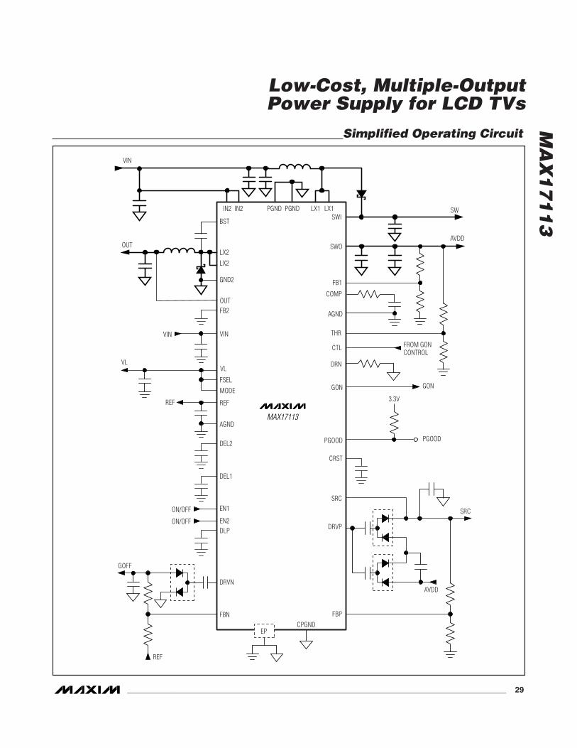
MA
X1
71
13
Low-Cost, Multiple-OutputPower Supply for LCD TVs
______________________________________________________________________________________ 29
LX2
REF
FB1
LX1 LX1
AGND
COMP
VIN
OUTAVDD
FSEL
FB2OUT
ON/OFF
ON/OFF
VL
VIN VIN
GON
3.3V
AGND
VL
REF
BST
GON
DRN
CTL FROM GONCONTROL
DRVN
FBNCPGND
REF
DRVP
FBP
SRC
PGND PGND
DEL2
DEL1
EN1
EN2
SWI
SWO
THR
DLP
MODE
SW
SRC
AVDD
IN2 IN2
LX2
GND2
GOFF
MAX17113
PGOODPGOOD
CRST
EP
Simplified Operating Circuit
MA
X1
71
13
Low-Cost, Multiple-OutputPower Supply for LCD TVs
Maxim cannot assume responsibility for use of any circuitry other than circuitry entirely embodied in a Maxim product. No circuit patent licenses areimplied. Maxim reserves the right to change the circuitry and specifications without notice at any time.
30 ____________________Maxim Integrated Products, 120 San Gabriel Drive, Sunnyvale, CA 94086 408-737-7600
© 2009 Maxim Integrated Products Maxim is a registered trademark of Maxim Integrated Products. Inc.
Chip InformationPROCESS: BiCMOS
Package InformationFor the latest package outline information and land patterns, goto www.maxim-ic.com/packages.
PACKAGE TYPE PACKAGE CODE DOCUMENT NO.
40 TQFN-EP T4055+1 21-0140