EUV High-NA scanner to extend EUV single exposure · Public quotes from major customers on EUV...
33
Jan van Schoot 1 , Eelco van Setten 1 , Gerardo Bottiglieri 1 , Kars Troost 1 , Sascha Migura 3 , Bernhard Kneer 3 , Jens Timo Neumann 3 , Winfried Kaiser 3 15 June 2016, EUVL Workshop, Berkeley EUV High-NA scanner to extend EUV single exposure Public 1 ASML Veldhoven, The Netherlands 2 ASML Wilton, CT, USA 3 Carl Zeiss Oberkochen, Germany
Transcript of EUV High-NA scanner to extend EUV single exposure · Public quotes from major customers on EUV...

Jan van Schoot1, Eelco van Setten1, Gerardo Bottiglieri1, Kars Troost1,
Sascha Migura3 , Bernhard Kneer3, Jens Timo Neumann3, Winfried Kaiser3
15 June 2016, EUVL Workshop, Berkeley
EUV High-NA scanner to extend EUV single exposure
Public
1 ASML Veldhoven, The Netherlands 2 ASML Wilton, CT, USA
3 Carl Zeiss Oberkochen, Germany

Public quotes from major customers on EUV adoption
Sources: Transcript, Intel Credit Suise Media conference, Brian Krzanich, December 2015, Source: Transcript, TSMC Q1 2016 earnings call, Mark Liu, April 2015, Joshua Ho,
Anand tech, “Samsung Foundry Updates: 7 nm EUV, 10 LPP, and 14LPC, April 22 2016
Brian Krzanich CEO Intel
Mark Liu, Co-CEO TSMC
EUV to shorten time to yield
in the next 5 yrs
EUV will be adopted for
production at N5
Intend do deploy EUV for 7
nm
25 February 2016
Slide 2
Public
DRAM Logic 55 WpH 125 WpH 185 WpH 145 WpH
NXE:3300B
NXE:3350B
NXE:3450C
High NA
7
3.0/5.0 nm
1.4/<2.0 nm
7.0 nm
2.5 nm
DCO/MMO OPO
110 nm
60 nm
Focus
NXE extension roadmap to optimize capital efficiency
1.0/<1.4 nm 1.5 nm <40 nm
1.5/2.5 nm 3.5 nm 70 nm
1.2/<1.7 nm 2.0 nm 50 nm
R&D
D1M
D1L
SNEP 3350B
NXE:3400B 5
<D1L
3.x
20% PFR illuminator
2~2.5
Products under study
D1H
2017
2015
2013
Roadmap: Nov 2015
1st
Shipment
22 nm
13 nm
<8 nm
16 nm
13 nm
Half pitch
UVLS
OFP 3350B3400B
UVLS – Mk2
SMASH – MkX
Anamorphic lens
Stages, handlers
Lens thermal
25 February 2016
Slide 3
Public

25 February 2016
Slide 4
Public
#Critical exposures for critical logic Further reduction of # exposures using EUV 0.55 NA
Source: Luc van den Hove, IMEC, ”Technologies for the intuitive internet of everything”, ITPC 2015,
High-
NA
ArF triple patterning
EUV single patterning
High-
NA

Larger NA reduces Local CDU Due to larger aerial image contrast
Jo Finders et al, SPIE 2016
0.33NA
0.55NA
Non-CAR resist, Quasar Illumination
25 February 2016
Slide 5
Public

0
20
40
60
80
100
120
140
160
180
200
10 12 14 16 18 20 22 24
Effe
ctiv
e T
PT
[wf/
hr]
(Final) Half Pitch [nm]
LCDU = 2.0nm 0.33
LCDU = 2.0nm 0.55
Larger NA results in higher effective throughput NA limits dose and # of LE steps
LE^2 LE^3
0.55NA @ 500W
0.33NA @ 350W
* Effective throughput = throughput / # LE steps
*
Quasar Illumination
25 February 2016
Slide 6
Public

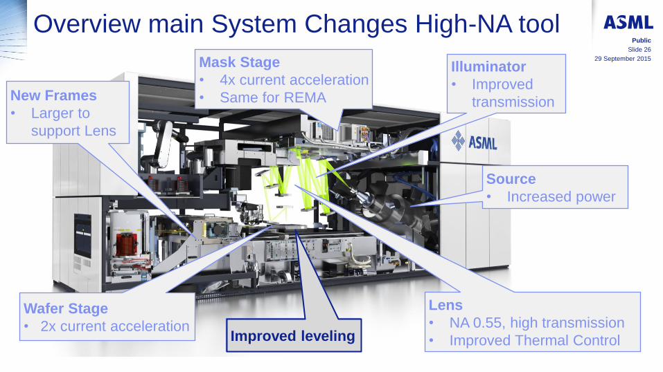
Overview main System Changes High-NA tool
Source
• Increased power
Lens
• NA 0.55, high transmission
• Improved Thermal Control
Mask Stage
• 4x current acceleration
• Same for REMA
Wafer Stage
• 2x current acceleration
Illuminator
• Improved
transmission New Frames
• Larger to
support Lens
29 September 2015
Slide 7
Public
Improved leveling

Overview main System Changes High-NA tool
Source
• Increased power
Lens
• NA 0.55, high transmission
• Improved Thermal Control
Mask Stage
• 4x current acceleration
• Same for REMA
Wafer Stage
• 2x current acceleration
Illuminator
• Improved
transmission New Frames
• Larger to
support Lens
29 September 2015
Slide 8
Public
Improved leveling
Lens
• NA 0.55, high transmission
• Improved Thermal Control

EUV: it’s all about the angle High-NA comes with large angles
ML reflection MoSi Multilayer
25 February 2016
Slide 9
Public
NA=0.5
30deg!!
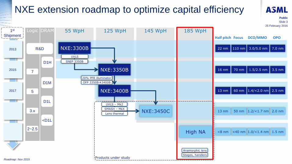
EUV Optical Train
intermediate focus
collector
Reticle (mask)
wafer
plasma
illuminator
field facet mirror
pupil facet mirror
projection
optics
source
25 February 2016
Slide 10
Public
W. Kaiser, J. van Schoot, Sematech Workshop on High-NA, 9 July 2013
Two key-area’s
where High-NA
imposes large
angles

projection optics Mag=4
w
effective line
width
Small angle
~1
20
nm
4x10nm = 40nm
Simple model of the optical column
Bending out the light cones at the mask reduces contrast strongly
j
illumination optics
source
mask
wafer
Large angle
effective line
width
w
We have to limit the
angles on the mask!
increase magnification
𝑁𝐴𝑚𝑎𝑠𝑘 =𝑁𝐴𝑤𝑎𝑓𝑒𝑟
𝑀𝑎𝑔
25 February 2016
Slide 11
Public
NAwafer
NAmask

Image contrast increases with a larger magnification But only needed in one orientation
NXE:3300
requirement
0
1
2
3
4 5 6 7 8
Magnification
Horizontal Lines
13 nm L/S, 0.33 NA (k1=0.318)
NIL
S*
8 nm L/S, 0.55 NA (k1=0.326)
High-NA tool
*NILS = Normalized Image Log Slope,
measure for image contrast
4 5 6 7 8
Magnification
Vertical Lines
NIL
S*
0
1
2
3
13 nm L/S, 0.33 NA (k1=0.318)
8 nm L/S, 0.55 NA (k1=0.326)
Anamorphic
magnification needed
for High-NA
25 February 2016
Slide 12
Public
J. Van Schoot, et al, “EUV lithography scanner for sub-8nm resolution,” Proc. SPIE 9422, (2015).

pupil
scan
wafer
scan
reticle
scan
• Anamorphic optics half field:
8x Magnification in scan
4x Magnification in other direction
• Chief ray angle ok Imaging ok
High-NA >0.5NA 4x/8x anamorphic magnification Chief Ray Angle at Mask can be maintained
Pupil-in
scan
Pupil-out
The pattern at the
mask needs to change
25 February 2016
Slide 13
Public

Mask
Wafer
Lens
High-NA Anamorphic Lens prints a half field By utilizing the current 6” mask
Mask
field
size
Wafer
field
size
104 mm
13
2 m
m
4x
26 mm
33
mm
4x Conventional lens
Full Field (FF)
HF
26 mm
16
.5 m
m
New
Half Field (HF)
QF
104 mm
13
2 m
m
4x/8x
Note: rectangular slit shown for illustration purposes
FF
25 February 2016
Slide 14
Public
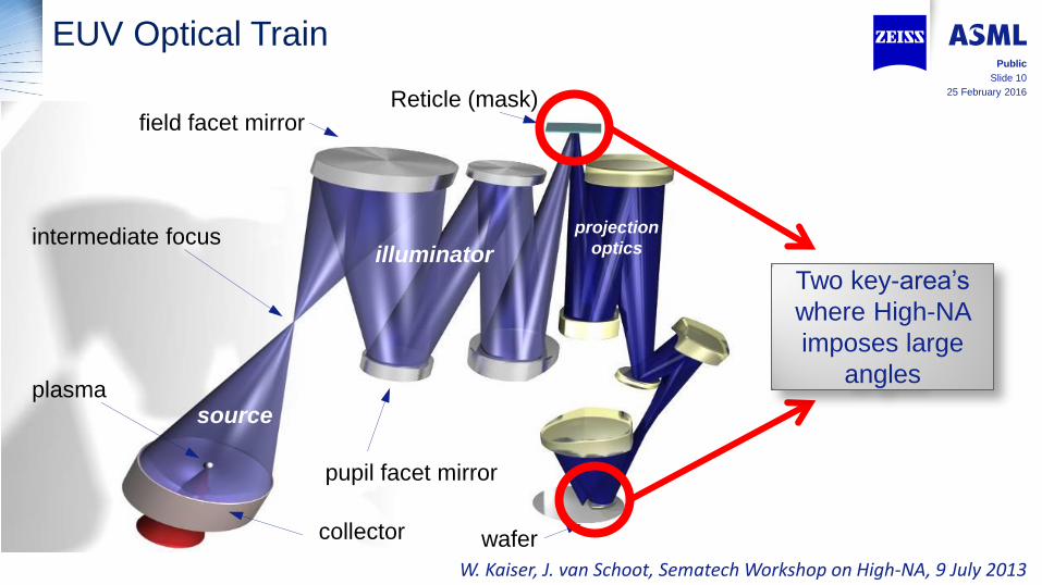
Anamorphic optics are used in cinematography “Don’t change the mask”
Anamorphic
Camera
Anamorphic
Projector
“The Mask”
(24x36mm2)
16x9 16x9
25 February 2016
Slide 15
Public

B. Kneer, et al, “EUV lithography optics for sub-9nm resolution,” Proc. SPIE 9422, (2015).
NA 0.25 NA 0.33 NA >0.5 Design examples Wafer
level
Reticle
level
Extreme aspheres enabling
further improved wavefront /
imaging performance
Big last mirror driven by
High NA
Tight surface specifications enabling
low straylight / high contrast imaging
25 February 2016
Slide 16
Public
High-NA optics design concepts available Larger elements with tighter specifications, no showstoppers

Imaging verification of the new Half Field concept
Aerial Image Intensity in Hyperlith
Logic N5 clip Metal-1, 11nm lines, SMO is done at 8x
FF QF HF
Note: pictures at same scale,
smaller mask reflection is
also visible
25 February 2016
Slide 17
Public

Angles and
angular spread
decrease
ob
scu
red
25 February 2016
Slide 18
Public
High-NA optics has ~2x transmission Smaller angles enable transmission gain vs non-obscured NA 0.33
un
ob
scu
red
And even better:
The smaller angular
range increases the
transmission
Substrate
Standard EUV coatings cannot
handle these large angles

25 February 2016
Slide 19
Public
Proven imaging performance with High-NA optics
Spaces through pitch with small annular illumination
• Start pitch: 24nm for high-NA, 40nm for NA 0.33 k1 = 0.49 in both cases. • Anamorphic high NA w/ central obscuration: comparable exposure latitude, @ smaller pitches. • Lower Best Focus variation for high NA.
HighNA obscured pupil
wafer

Overview main System Changes High-NA tool
Source
• Increased power
Lens
• NA 0.55, high transmission
• Improved Thermal Control
Mask Stage
• 4x current acceleration
• Same for REMA
Wafer Stage
• 2x current acceleration
Illuminator
• Improved
transmission New Frames
• Larger to
support Lens
29 September 2015
Slide 20
Public
Improved leveling
Illuminator
• Improved
transmission

Principle NXE:3300/3400 illuminator can be reused For anamorphic lithography pupil facet mirror becomes asymmetric
Intermediate
Focus
Field Facet Mirror
Pupil Facet Mirror
25 February 2016
Slide 21
Public

Overview main System Changes High-NA tool
Source
• Increased power
Lens
• NA 0.55, high transmission
• Improved Thermal Control
Mask Stage
• 4x current acceleration
• Same for REMA
Wafer Stage
• 2x current acceleration
Illuminator
• Improved
transmission New Frames
• Larger to
support Lens
29 September 2015
Slide 22
Public
Improved leveling
Mask Stage
• 4x current acceleration
• Same for REMA
Wafer Stage
• 2x current acceleration
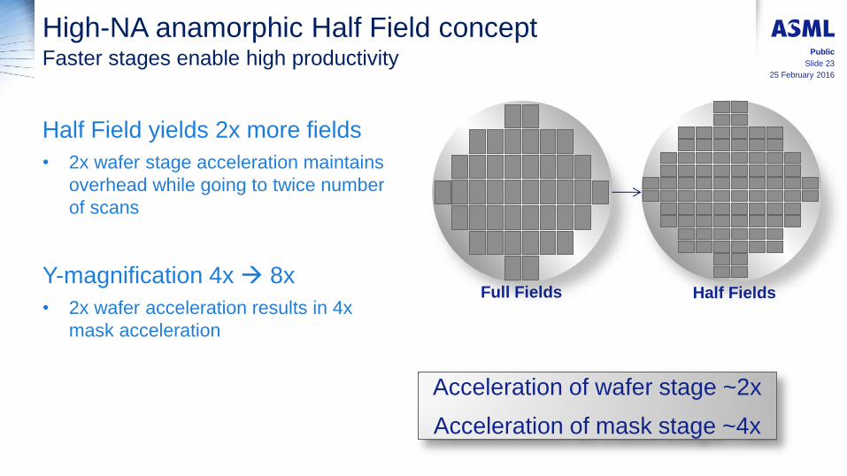
High-NA anamorphic Half Field concept
Half Field yields 2x more fields
• 2x wafer stage acceleration maintains
overhead while going to twice number
of scans
Y-magnification 4x 8x
• 2x wafer acceleration results in 4x
mask acceleration
Faster stages enable high productivity
Full Fields Half Fields
Acceleration of wafer stage ~2x
Acceleration of mask stage ~4x
25 February 2016
Slide 23
Public

0
5
10
80
110
140
170
200
0 1 2 3 4
Rela
tiv
e R
MS
RS
Po
wer
Th
rou
gh
Pu
t [w
ph
]
Relative RS acceleration in Y-direction
0
5
10
80
110
140
170
200
0 1 2 3 4
Rela
tiv
e R
MS
RS
Po
wer
Th
rou
gh
Pu
t [w
ph
]
Relative RS acceleration in Y-direction
0
5
10
80
110
140
170
200
0 1 2 3 4
Rela
tiv
e R
MS
RS
Po
wer
Th
rou
gh
Pu
t [w
ph
]
Relative RS acceleration in Y-direction
High-NA Mask Stage solution for increased acceleration Improved motor technology & different architecture
185
125
ref
870%
390%
∞!
Further Optimizing power
consumption:
• New stage architecture with
lower mass
Limiting increasing power by:
• Improved motor technology (k, R)
• Reduce mass
Current RS in High-NA
Power: ref
Current RS
No solution
Improved RS motor
Power: 9 x ref
x
x
x x x x
4x
25 February 2016
Slide 24
Public
Power ~ 𝐼2 ∙ 𝑅
= 𝑘 ∙ 𝑎𝑐𝑐 ∙ 𝑚𝑎𝑠𝑠 2 ∙ 𝑅𝑚𝑜𝑡𝑜𝑟
Courtesy Chris Hoogendam, ASML

High-NA Field and Mask Size productivity 500W enables throughput of >150wph with anamorphic HF
High-NA Half Field scanner
needs 500W for
150wph at 60mJ/cm2
Thro
ugh
pu
t [3
00
mm
/hr]
Source Power/Dose [W/(mJ/cm2]
Throughput for various source powers and doses
0
20
40
60
80
100
120
140
160
180
200
0 5 10 15 20 25 30 35
500 Watt
60mJ/cm2
500W Watt
30mJ/cm2
NXE:3300
WS, RS current performance
WS 2x, RS 4x
HF
High NA anamorphic
FF
25 February 2016
Slide 25
Public
Overview main System Changes High-NA tool
Source
• Increased power
Lens
• NA 0.55, high transmission
• Improved Thermal Control
Mask Stage
• 4x current acceleration
• Same for REMA
Wafer Stage
• 2x current acceleration
Illuminator
• Improved
transmission New Frames
• Larger to
support Lens
29 September 2015
Slide 26
Public
Improved leveling Improved leveling

High-NA calls for tight focus control High-NA scanner will be introduced in line with focus scaling
focus control budget
at introduction
25 February 2016
Slide 27
Public
𝐷𝑜𝐹 = 𝑘2
λ
𝑁𝐴2
Rayleigh
k2 = 1
NXE:3300
High-NA

Focus latitude scales according expectation
Spaces through pitch with small annular illumination
Focus [nm] -50 0 -50 -25 25
1.0
1.8
I 0 [
a.u
.]
NA 0.55, 12nm spaces
1.4
1.6
1.2
Focus [nm] -75 -150 0 -150 75
1.0
1.8
I 0 [
a.u
.]
NA 0.33, 20nm spaces
1.4
1.6
1.2
25 February 2016
Slide 28
Public
150nm 50nm
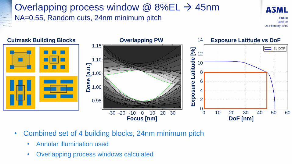
Overlapping process window @ 8%EL 45nm
• Combined set of 4 building blocks, 24nm minimum pitch
• Annular illumination used
• Overlapping process windows calculated
NA=0.55, Random cuts, 24nm minimum pitch 25 February 2016
Slide 29
Public
Cutmask Building Blocks Overlapping PW
Focus [nm]
Do
se
[a
.u.]
-30 -20 -10 0 30 20 10
0.95
1.00
1.05
1.10
1.15 Exposure Latitude vs DoF
DoF [nm]
Exp
osu
re L
ati
tud
e [
%]
0 30 20 10 60 50 40 0
6
4
2
12
10
8
14

High-NA system has smaller M3D effects than 0.33NA
Smaller mask angles of incidence due to anamorphic system
(4x)
*L. de Winter, Understanding the Litho-impact of Phase due to 3D Mask-Effects when using off-axis illumination, EMLC 2015
Two-bar trenches are a
canary for M3D effects
25 February 2016
Slide 30
Public
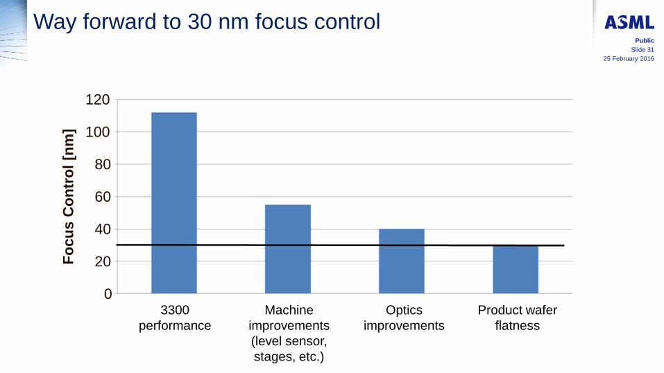
Way forward to 30 nm focus control
3300
performance
Machine
improvements
(level sensor,
stages, etc.)
Optics
improvements
Product wafer
flatness
Fo
cu
s C
on
tro
l [n
m]
0
20
40
60
80
100
120
25 February 2016
Slide 31
Public

Summary
• High-NA extends Moore’s Law into the next decade
• Larger contrast of High-NA helps mitigating LCDU
• New anamorphic concept enables good imaging with existing
mask infrastructure resulting in a Half Field image
• New stages technologies and high transmission enable throughput
~185WpH
• We identified measures to meet the tight focus budget
25 February 2016
Slide 32
Public
The authors would like to thank the High-NA teams in - Oberkochen - Wilton - Veldhoven
Public
Thank you
for your attention