ESD and Mechanical Design Donn G. Bellmore …File/ESDandMechanicalDesign.prn.pdf · ESD and...
13
ESD and Mechanical Design Donn G. Bellmore Systems Engineering Analyst Universal Instruments Corporation 607 779 7471 [email protected] Abstract: Automated Component Handling (ACH) and Automated Handling Equipment (AHEs) manufacturers have been aware of ESD and the damage it causes to devices for quite sometime. ESD damage to components through various failure modes such as Human Body Model, Charged Device Model, and Machine Model have been well documented and discussed with more research being done all the time. The need for component packaging to protect component and devices from Static Electricity has also been well documented, however, with new technologies emerging all the time allowing greater throughput and smaller area population, packaging is and will play even a greater roll in performance. ESD effects of automated component packaging such as carrier tapes can and will affect performance of high-speed equipment. In making decisions regarding packaging, ESD concerns in protecting sensitive components are no longer the only concerns but what ESD requirements are also needed to prevent reductions in system performance due to ESD. This paper discusses the ESD measurement and mechanical test methods, and results of completed tests on various qualities and configurations of chip packaging materials and the effects on various prototype equipment performances. As a result, conclusions and recommendations will be made regarding specific types of packaging for specific types of components used in various types of automated equipment. Included in the results is high-speed documentation displaying the effects of ESD charging on chips, packaging, and the effects on system performance. Introduction: Electrostatic Electricity (ESD) hazards to the reliability of electronic devices and assemblies have been well documented for quite some time. As devices become smaller, faster, and use less power, they are becoming more sensitive to ESD. The component manufactures have been challenged to find economical methods and packaging to safely store and transport sensitive components such as recommended in EIA-541. Users are constantly being challenged to provide static safe environments to process new technologies in an economical manner. Manufactures are also being challenged to design and manufacture assembly equipment that will process devices safely while doing so faster, more accurate, and at a lower cost.
Transcript of ESD and Mechanical Design Donn G. Bellmore …File/ESDandMechanicalDesign.prn.pdf · ESD and...

ESD and Mechanical DesignDonn G. Bellmore
Systems Engineering AnalystUniversal Instruments Corporation
607 779 [email protected]
Abstract:Automated Component Handling (ACH) and Automated Handling Equipment(AHEs) manufacturers have been aware of ESD and the damage it causes todevices for quite sometime. ESD damage to components through various failuremodes such as Human Body Model, Charged Device Model, and Machine Modelhave been well documented and discussed with more research being done all thetime. The need for component packaging to protect component and devices fromStatic Electricity has also been well documented, however, with new technologiesemerging all the time allowing greater throughput and smaller area population,packaging is and will play even a greater roll in performance. ESD effects ofautomated component packaging such as carrier tapes can and will affectperformance of high-speed equipment. In making decisions regarding packaging,ESD concerns in protecting sensitive components are no longer the only concernsbut what ESD requirements are also needed to prevent reductions in systemperformance due to ESD. This paper discusses the ESD measurement andmechanical test methods, and results of completed tests on various qualities andconfigurations of chip packaging materials and the effects on various prototypeequipment performances. As a result, conclusions and recommendations will bemade regarding specific types of packaging for specific types of components usedin various types of automated equipment. Included in the results is high-speeddocumentation displaying the effects of ESD charging on chips, packaging, andthe effects on system performance.
Introduction:
Electrostatic Electricity (ESD) hazards to the reliability of electronic devices andassemblies have been well documented for quite some time. As devices becomesmaller, faster, and use less power, they are becoming more sensitive to ESD.The component manufactures have been challenged to find economical methodsand packaging to safely store and transport sensitive components such asrecommended in EIA-541. Users are constantly being challenged to providestatic safe environments to process new technologies in an economical manner.Manufactures are also being challenged to design and manufacture assemblyequipment that will process devices safely while doing so faster, more accurate,and at a lower cost.

ESD and Mechanical Design
Page 2
Recently while performing system verifications on prototype equipment, it wasobserved at times, a large amount of missed picked parts. It was determined thatthe large number of missed picked parts were consistent with several factors, typeof component, size of component, humidity, and packaging materials. In otherwords, the smaller chips such as 0603s and 0402s in some packaging did notperform as well. With automatic processing components such as 0603s, 0402s,0201s, and some 0805s, the mechanics become more difficult. Also as theweights of these components continue to drop, the sensitivity to CoulombicInteraction (attraction and repelling) increases and proper ESD Packagingbecomes more important not so much as to protect the devices but to insure a highdegree of mechanical reliability and performance. Mechanical devices designedto process these types of components must also be more robust to maintain highperformance. Also, as these charged components are being processed, what ishappening to adjacent components already placed that may be ESD Sensitive. Astudy was initiated to evaluate the ESD results of processing various componentswith different styles of packaging.
When researching the Standards such as EIA/IS-726 and EIA-481-B forrecommended taping characteristics, I was referred to Standard EIA-541 for ESDDescriptions and terminology. These standards address the mechanics of tapingproperties and packaging material requirements for handling and storing sensitivecomponents, however, they fall short in describing and recommending materialsfor automated handling of sensitive components as well as packaging foroptimized mechanical performance.
The Experiment:
Purpose:The purpose of the test was to evaluate the various packaging types andcomponents to determine the overall ESD Characteristics and the effects onperformance with prototype feeders.
Set Up:The tests were conducted on the bench with a feeder set up as indicated by thefollowing Photos and on a number of machines tracking Parts Per Million (PPM)
Defect Rates. The bench testing used afeeder test controller capable of singlecycle and continuous cycle that simulatethe machine function. The Machine tests consisted of severalmachines using these products topopulate test boards. Not all of the samemanufactures and types were used forboth studies due to time and availability;however, the different characteristicswere represented in both types of tests.

ESD and Mechanical Design
Page 3
See arrows for Voltage Sensor and Component Pick UpAs the components are indexed, the cover tape is monitored and the componentsare picked up by vacuum to prevent jamming the feeder. The componentsmeasured were measured while in the pockets.
These photos are of the modified peeler used to view the components in the pockets priorto peeling the cover tape back. As one can see a section was removed from the peeler togain viewing access and to allow for static voltage measurements at a close proximity tothe peeling function. Correlations of the measurements indicate that these measurements
VoltageSensor
VacuumComponentPick Up

ESD and Mechanical Design
Page 4
made in this location will be somewhat less than if made off of the peeler entirely due tofield absorption.
This Photo is one of the set ups for High SpeedMotion analysis and was used to obtain the highspeed AWIs from which the various pictures camefrom as still frames. They will be seen later underthe results. Note that in this set up, the cover tapewas held up to allow for viewing under the peeledcover. See the arrow for the high speed BoreScope Lens.
This photo indicates theposition of the voltagemeasurement probe whilemonitoring the voltage levelsof the tape being unreeled.
Results:The following Tables 1 and 2 are the results of the measurements made, the typesof components and packaging used for processing, and comments specific to theperformance.
Table 1 provides a list of component types, the average weight of eachcomponent in grams, the type of packaging, paper or plastic, stamped orthermo formed, and the voltage measurements of the packaging andresultant voltage on the component. Temperature was between 70 to 73degrees F. and Humidity was as indicated.

ESD and Mechanical Design
Page 5
Table 1
Table 2 provides a list of resultant voltages on the components and theresistance of the packaging and specific comments. The resistance formost of the packaging regardless of color (black, clear, or white), was10e11 ohms with a few exceptions.
Component Type Weight Grams Feeder Tape Type
Cover Tape
Carrier Tape
Bottom Tape Comp.
20.6 0201 - C 0.00031 8 mm Paper stamped -96 -2000 -3000 NA19.9 0201 - R 0.00014 8 mm Paper stamped -50 -500 -400 3019 0402 - C 0.00125 8 mm Paper stamped -200 -700 -700 5019 0402 - C 0.00088 8 mm Paper stamped -60 -81 -81 2519 0402 - C 0.0026 8 mm Paper stamped -30 25 20 10
21.5 0402 - C 0.0017 8 mm Thermo Form -26 30 30 021.2 0402 - R 0.0011 8 mm Paper stamped -300 -1000 -1000 5020.8 0402 - R 0.00075 8 mm Paper stamped -850 -3000 -3000 7521.7 0402 - R 0.0006 8 mm Paper stamped -2000 -800 -800 6033 0603 - C 0.0056 8 mm Paper stamped -5 7 019 0603 - C 0.0058 8 mm Paper stamped -1000 750 800 50
21.6 0603 - C 0.0055 8 mm Thermo Form 800 6000 3000 2021.6 0603 - C 0.007 8 mm Thermo Form 2000 -4700 -5700 5020.6 0603 - C 0.0058 8 mm Paper stamped 2000 -160 -150 -1518.9 0603 - R 0.0025 8 mm Paper stamped -1050 900 840 30
19 0603 - R 0.0025 8 mm Paper stamped -1050 800 740 5033 0603 - R 0.0029 8 mm Paper stamped -20 100 100 019 0603 - R 0.0035 8 mm Paper stamped
19 0805 - C 0.017 8 mmPlastic stamped -1000 3000 3000 100
18.9 0805 - C 0.0091 8 mm Paper stamped -100 170 140 0
20 0805 -R 0.005 8 mmPlastic stamped -1000 7000 7000 15
38 - 42 LEDs 0603s 0.002 8 mm Thermo Form -500 15 0 1538 - 42 LEDs 0603s 0.002 8 mm Thermo Form -50 15 0 15
38 - 42 LEDs 0603s 0.002 8 mm Thermo Form -675 0 60038 - 42 LEDs 0603s 0.002 8 mm Thermo Form 15 0 1538 - 42 LEDs 0603s 0.002 8 mm Thermo Form -200 -15 -200 15
38 - 42 LEDs 0603s 0.002 8 mm Thermo Form -1100 -1100 20
23.3 PLCC 44 NA 32 mm Thermo Form 2000 0 0 15022 SOIC 16 NA 16 mm Thermo Form 3 0 0 023 SOIC 8 NA 12 mm Thermo Form -200 0 0 30
Charge Generation, VoltsProduct DescriptionRelative Humidity
RH %

ESD and Mechanical Design
Page 6
Table 2
The following are consequences of charged 0603 components and degradation ofperformance. They are single frames taken from high speed motion analysisvideos and saved as single frames.
Comp. Voltage
Cover Tape
Carrier Tape
Bottom tape Comments
NA 1.00E+12 1.00E+12 1.00E+12
30 1.00E+12 1.00E+12 1.00E+12Every other to every components was pulled from the pocket and traveled up the cover.
50 1.00E+12 1.00E+12 1.00E+12 Carrier Tape out of scrap chute at 1000 Volts
25 1.00E+12 1.00E+12 1.00E+12Classified as problem, material appears to be low charging. Decay time is rapid
10 1.00E+12 1.00E+12 1.00E+120 1.00E+11 50000 50000 Parts ran very good, even with old peeler.
50 1.00E+12 1.00E+12 1.00E+12Classified as a problem, components are pulled from pockets by attraction to cover tape.
75 1.00E+11 1.00E+12 1.00E+12Classified as a problem, components are pulled from pockets by attraction to cover tape.
60 1.00E+12 1.00E+12 1.00E+12Classified as a problem, components are pulled from pockets by attraction to cover tape.
0 1.00E+12 1.00E+12 1.00E+12
50 1.00E+12 1.00E+12 1.00E+12Classified as a problem, components are pulled from pockets by attraction to cover tape.
20 1.00E+11 1.00E+12 1.00E+12Tape is charged to several hundred volts as it is coming off the reel and before peeler.
50 1.00E+11 1.00E+11 1.00E+11 Parts stick in pocket, +comp with -tape, reverse attraction-15 1.00E+11 1.00E+12 1.00E+12 Parts stayed in pockets, hard to remove.
30 1.00E+12 1.00E+12 1.00E+12Large Amount of paper fuzz on cover tape, paper bottom. Parts are attracted to cover tape.
50 1.00E+12 1.00E+12 1.00E+12+ 60 volts on tape as unreeled, Paper fuzz on cover tape increases charge and attraction, 200 V.
0 1.00E+12 1.00E+12 1.00E+121.00E+12 1.00E+12 1.00E+12
100 1.00E+12 1.00E+12 1.00E+12Classified as a problem, components are pulled from pockets by attraction to cover tape.
0 1.00E+12 1.00E+12 1.00E+12Not listed as a problem, however, it appears the paper fuzz on the cover tape charges and attracts components.
15 1.00E+12 1.00E+12 1.00E+12Highly chargeable materials used. If antistatic, properties have dissipated
15 1.00E+12 1.00E+07 NA15 1.00E+12 1.00E+07 NA
600 1.00E+12 1.00E+07 NAComponents would attract to cover tape over 450 volts in 5 minutes run time and charge would last for 2 to 3 minutes
15 1.00E+12 1.00E+07 NA15 1.00E+12 1.00E+12 1.00E+12 Carrier Tape is low charging, cover tape is not
20 1.00E+12 1.00E+12 1.00E+12Charge occurred in processing or indexing 10 components. Parts were attracted to cover tape.
150 1.00E+12 1.00E+06 1.00E+06
150 volts measured with field probe, 50 volts measured with High imp. Voltage probe. The rolled up cover tape was generating 6000 volts within .5 inches of the taped components without the benefit of static shielding.
0 1.00E+11 1.00E+07 1.00E+07 There was no apparent charge to measure. 30 1.00E+11 1.00E+06 1.00E+07 Components lead frame was charged to 30 volts.

ESD and Mechanical Design
Page 7
These are high-speed photos of consecutive positive charged 603 capacitorpulled out of the pockets by attraction to the negative charged cover tape.The tape was -100 volts while the component was 50 volts.

ESD and Mechanical Design
Page 8
The 0603 capacitor was lifted in the pocket as it came out from under thepeeler, it was then like a big spring and as soon as it was free, it launched.The next few photos show the trajectory as it lands into the next pocket.That part may be hard to explain in real time.
ESD and Mechanical Design
Page 9
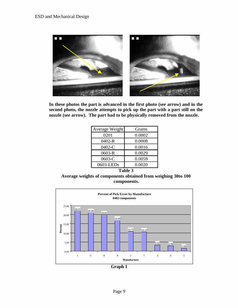
In these photos the part is advanced in the first photo (see arrow) and in thesecond photo, the nozzle attempts to pick up the part with a part still on thenozzle (see arrow). The part had to be physically removed from the nozzle.
Table 3Average weights of components obtained from weighing 30to 100
components.
Graph 1
Average Weight Grams0201 0.0002
0402-R 0.00080402-C 0.00160603-R 0.00290603-C 0.0059
0603-LEDs 0.0020
Percent of Pick Error by Manufacture0402 components
22.1120.98
19.91
16.80
10.75 10.47
3.42 2.961.66
0.00
5.00
10.00
15.00
20.00
25.00
I U 9 8 J 7 2 S 5
Manufacture
Perc
ent

ESD and Mechanical Design
Page 10
Graph 2
Graph 3
Percent of Pick Error by Manufacture0603 Components
39.72
24.10
12.8511.68
5.50 4.45
1.02 0.68 0.000.00
5.00
10.00
15.00
20.00
25.00
30.00
35.00
40.00
45.00
G 5 L 8 9 K 6 7 3
Manufacture
Per
cent
PPM By Manufacture 0402 component
2500
1583
1354
208 208104
0 00
500
1000
1500
2000
2500
3000
I J S 9 2 5 8
Manufacture
PPM
Def
ects

ESD and Mechanical Design
Page 11
Graph 4
Conclusions:
1. With an average weight of .0016 grams for 0402 capacitors, (Tables 2 and 3)coulombic interaction (attraction and repelling) can result with as little as 50volts on the cover tape.
2. With an average weight of .0002 grams for 0201s, (Tables 2 and 3) coulombicinteraction can result with as little as 25 volts on the cover tape.
3. Based on tables 1 and 2, the packaging materials tested ranged from staticdissipative to low charging (anti-static) materials. Low charging is thepreferred term in the ESD industry. Since resistance properties are usually nottied to low charging materials, it is difficult to determine. However, somecover tapes charged up very easily to 1000 to 2000 volts while other did not.While some tapes charged up, the charged decayed rapidly. Most lowcharging materials of these types have a shelf life and some packaging mayhave expired since the low charging properties were inconsistent between thesame manufacture.
4. There is another factor referred to as wind up tension that causes aninconsistent charging through out the same reel. The winding up of the carriertape places the cover tape under tension that causes the low chargingsurfactant to degrade or break down in spots. At one point the voltage levelcould be an order of magnitude higher than another point on the same reel.Consequently, the act of reeling up the carrier and cover tapes must cause aninconsistent low charging characteristic.
PPM by Manufacture 0603 component
931
496 496
372
186
93
0 0 00
100
200
300
400
500
600
700
800
900
1000
5 G L 8 9 K 3 6 7
Manufacture
PP
M D
efec
ts

ESD and Mechanical Design
Page 12
5. Based on Tables 1 and 2, and Graphs 1 through 4, there is a correlationbetween poor packaging and higher defects rates. The higher the charge on thecomponent and carrier system, the higher the defect rate. While not allmanufactures were tested in each set of tests, the types and characteristics ofthe packaging was represented in both tests.
6. Handling devices have to be robust enough to handle these types of issues,however, as the components get smaller, see Table 3, for example, a 0201component weighs .0002 grams, ESD issues will become an even greaterfactor. The packaging materials of these components may need to bedissipative or conductive to prevent charging of the component and therebyreduce ESDA defects. Work will have to continue in this area.
7. End users need to be aware of the differences in packaging materials. Anti-Static or low charging materials do not necessarily mean the problems aresolved. As seen in Tables 1 and 2, there is a significant difference betweenthem. There are self-life, tension wind up, and quality issues affecting thepackaging. The amount of charge measured on the components, please seeTable 1, LEDs and PLCCs charged up to 600 volts and 150 volts respectively,cannot be good for the process. A side note is that while the PLCCs werepackaged in dissipative carrier tape, the cover tape was a low chargingmaterial, consequently, the components saw very little or no benefits of staticshielding.
8. End Users, Equipment, and Component Manufactures have to work very closetogether to provide greater protection to sensitive assemblies and insure theoptimum process performance at the lowest cost. It all becomes a businessdecision regarding the cost of components, cost of packaging, and the cost ofadditional robustness of the handling devices.
9. Low Charging materials are no longer sufficient for many of these types ofcomponents. Static Dissipative materials may be required to improve andinsure handling performance.
10. Standards EIA/IS-726 and EIA-481-B need to have an appendix or a sectionbriefly describing various ESD related terms and applications where suchmaterials may be used. Standards are intended to be helpful, to provideeducation specific to an application or process, and to provide guidance forconsistent processes. One should not have to read one standard and bereferred to other standards unless greater detail is desired.
Test Equipment Used:
Trek Model 368 Electrostatic Voltmeter Trek Miniature Probe3 M Megohm meter Feeder Test ControllerTrek 152P-2P Surface Resistance Probe GSM Platform

ESD and Mechanical Design
Page 13
References:
ESD Association ESD STM4.1-1997 EIA-541, June 1988ESD Association ESD SP10.1-2000 EIA / IS-726, October 1997ESD Association ESD STM11.11-2001 ANSI/ EIA-481-B-2001ESD Association ESD STM11.12-2001ESD Association ESD-ADV-1.0-1994
Acknowledgements:
I would like to thank Mr. Paul Nush, Mr. Ricky Heath, and Mr. Filippo Muggeo,who provided the necessary support by conducting the test on the machines,assisted during Lab testing, and collecting data.