ENHANCEMENT OF POWER QUALITY IMPROVEMENT … Papers/IJMTARC-170613.pdf · ENHANCEMENT OF POWER...
7
INTERNATIONAL JOURNAL OF MERGING TECHNOLOGY AND ADVANCED RESEARCH IN COMPUTING IJMTARC – VOLUME – V – ISSUE - 18 – JUNE , 2017 ISSN: 2320-1363 ENHANCEMENT OF POWER QUALITY IMPROVEMENT GRID-CONNECTED DUAL VOLTAGE SOURCE INVERTER 1. MANTHENA RAGHUVARAN, 2. G RATNA KUMARI 3 RAMAVATH SHANKAR NAIK 1.Pg Scholar, Department of EEE, SLC's Institute of Engineering and Technology,Hyderabad. 2.Assistant Professor Department Of EEE, SLC's Institute of Engineering and Technology, Hyderabad. .3.Associate Professor& HOD, Department Of EEE, SLC's Institute of Engineering and Technology, Hyderabad ABSTRACT: The main aim of project is to improve the power quality by using fuzzy based grid connected dual voltage source inverter. The new scheme is comprised of two inverters, which enables the microgrid to exchange power generated by the distributed energy resources (DERs) and also to compensate the local unbalanced and nonlinear load. The control algorithms are developed based on instantaneous symmetrical component theory (ISCT) to operate DVSI in grid sharing and grid injecting modes. The proposed scheme has increased reliability, lower bandwidth requirement of the main inverter, lower cost due to reduction in filter size, and better utilization of microgrid power while using reduced dc-link voltage rating for the main inverter. These features make the DVSI scheme a promising option for microgrid supplying sensitive loads. the proposed topology validated through simulation results. Index Terms: Power quality, Distributed energy source,Fuzzycontroller,Grid connected inverter, instantaneous symmetrical component theory (ISCT). I.INTRODUCTION The proliferation of power electronics devices and electrical loads with unbalanced nonlinear currents has degraded the power quality in the power distribution network. Moreover, if there is a considerable amount of feeder impedance in the distribution systems, the propagation of these harmonic currents distorts the voltage at the point of common coupling (PCC). At the same instant, industry automation has reached to a very high level of sophistication, where plants like automobile manufacturing units, chemical factories, and semiconductor industries require clean power. For these applications, it is essential to compensate nonlinear and unbalanced load currents. Load compensation and power injection using grid interactive inverters in microgrid have been presented in the literature. A single inverter system with power quality enhancement is discussed in. The main focus of this work is to realize dual functionalities in an inverter that would provide the active power injection from a solar PV system and also works as an active power filter, compensating unbalances and the reactive power required by other loads connected to the system. In , a voltage regulation and power flow control scheme for a wind energy system (WES) is proposed. A distribution static compensator (DSTATCOM) is utilized for voltage regulation and also for active power injection. The control scheme maintains the power balance at the grid terminal during the wind variations using sliding mode control. A multifunctional power electronic converter for the DG power system is described. This scheme has the capability to inject power generated by WES and also to perform as a harmonic compensator. Most of the reported literature in this area discuss the topologies and control algorithms to provide load compensation capability in the same inverter in addition to their active power injection. When a grid-connected inverter is used for active power injection as well as for load compensation, the inverter capacity that can be utilized for achieving the second objective is decided by the available instantaneous microgrid real power. Considering the case of a grid- connected PV inverter, the available capacity of the inverter to supply the reactive power becomes less during the maximum solar insolation periods. At the same instant, the reactive power to regulate the PCC voltage is very much needed during this period. It indicates that providing multi functionalities in a single inverter degrades either the real power injection or the load compensation capabilities. This paper demonstrates a dual voltage source inverter (DVSI) scheme, in which the power generated by the microgridis injected as real power by the main voltage source inverter (MVSI) and the reactive, harmonic, and unbalanced load compensation is performed by auxiliary voltage source inverter (AVSI). This has an advantage that the rated capacity of MVSI can always be used to inject
-
Upload
trinhthien -
Category
Documents
-
view
219 -
download
0
Transcript of ENHANCEMENT OF POWER QUALITY IMPROVEMENT … Papers/IJMTARC-170613.pdf · ENHANCEMENT OF POWER...

INTERNATIONAL JOURNAL OF MERGING TECHNOLOGY AND ADVANCED RESEARCH IN COMPUTING
IJMTARC – VOLUME – V – ISSUE - 18 – JUNE , 2017 ISSN: 2320-1363
ENHANCEMENT OF POWER QUALITY IMPROVEMENT GRID-CONNECTED
DUAL VOLTAGE SOURCE INVERTER
1. MANTHENA RAGHUVARAN, 2. G RATNA KUMARI 3 RAMAVATH
SHANKAR NAIK
1.Pg Scholar, Department of EEE, SLC's Institute of Engineering and Technology,Hyderabad.
2.Assistant Professor Department Of EEE, SLC's Institute of Engineering and Technology, Hyderabad.
.3.Associate Professor& HOD, Department Of EEE, SLC's Institute of Engineering and Technology,
Hyderabad
ABSTRACT:
The main aim of project is to improve the
power quality by using fuzzy based grid connected dual
voltage source inverter. The new scheme is comprised of
two inverters, which enables the microgrid to exchange
power generated by the distributed energy resources
(DERs) and also to compensate the local unbalanced
and nonlinear load. The control algorithms are
developed based on instantaneous symmetrical
component theory (ISCT) to operate DVSI in grid
sharing and grid injecting modes. The proposed scheme
has increased reliability, lower bandwidth requirement
of the main inverter, lower cost due to reduction in
filter size, and better utilization of microgrid power
while using reduced dc-link voltage rating for the main
inverter. These features make the DVSI scheme a
promising option for microgrid supplying sensitive
loads. the proposed topology validated through
simulation results.
Index Terms: Power quality, Distributed energy
source,Fuzzycontroller,Grid connected inverter,
instantaneous symmetrical component theory (ISCT).
I.INTRODUCTION
The proliferation of power electronics devices
and electrical loads with unbalanced nonlinear currents has
degraded the power quality in the power distribution
network. Moreover, if there is a considerable amount of
feeder impedance in the distribution systems, the
propagation of these harmonic currents distorts the voltage
at the point of common coupling (PCC). At the same
instant, industry automation has reached to a very high
level of sophistication, where plants like automobile
manufacturing units, chemical factories, and semiconductor
industries require clean power.
For these applications, it is essential to
compensate nonlinear and unbalanced load currents. Load
compensation and power injection using grid interactive
inverters in microgrid have been presented in the literature.
A single inverter system with power quality enhancement is
discussed in. The main focus of this work is to realize dual
functionalities in an inverter that would provide the active
power injection from a solar PV system and also works as
an active power filter, compensating unbalances and the
reactive power required by other loads connected to the
system. In , a voltage regulation and power flow control
scheme for a wind energy system (WES) is proposed. A
distribution static compensator (DSTATCOM) is utilized
for voltage regulation and also for active power injection.
The control scheme maintains the power balance at the grid
terminal during the wind variations using sliding mode
control. A multifunctional power electronic converter for
the DG power system is described. This scheme has the
capability to inject power generated by WES and also to
perform as a harmonic compensator. Most of the reported
literature in this area discuss the topologies and control
algorithms to provide load compensation capability in the
same inverter in addition to their active power injection.
When a grid-connected inverter is used for active power
injection as well as for load compensation, the inverter
capacity that can be utilized for achieving the second
objective is decided by the available instantaneous
microgrid real power. Considering the case of a grid-
connected PV inverter, the available capacity of the
inverter to supply the reactive power becomes less during
the maximum solar insolation periods.
At the same instant, the reactive power to
regulate the PCC voltage is very much needed during this
period. It indicates that providing multi functionalities in a
single inverter degrades either the real power injection or
the load compensation capabilities. This paper
demonstrates a dual voltage source inverter (DVSI)
scheme, in which the power generated by the
microgridis injected as real power by the main voltage
source inverter (MVSI) and the reactive, harmonic, and
unbalanced load compensation is performed by auxiliary
voltage source inverter (AVSI). This has an advantage that
the rated capacity of MVSI can always be used to inject

INTERNATIONAL JOURNAL OF MERGING TECHNOLOGY AND ADVANCED RESEARCH IN COMPUTING
IJMTARC – VOLUME – V – ISSUE - 18 – JUNE , 2017 ISSN: 2320-1363
real power to the grid, if sufficient renewable power is
available at the dc link.
In the DVSI scheme, as total load power is
supplied by two inverters, power losses across the
semiconductor switches of each inverter are reduced. This
increases its reliability as compared to a single inverter
with multifunctional capabilities. Also, smaller size
modular inverters can operate at high switching frequencies
with a reduced size of interfacing inductor, the filter cost
gets reduced. Moreover, as the main inverter is supplying
real power, the inverter has to track the fundamental
positive sequence of current. This reduces the bandwidth
requirement of the main inverter. The inverters in the
proposed scheme use two separate dc links. Since the
auxiliary inverter is supplying zero sequence of load
current, a three-phase three-leg inverter topology with a
single dc storage capacitor can be used for the main
inverter. This in turn reduces the dc-link voltage
requirement of the main inverter. Thus, the use of two
separate inverters in the proposed DVSI scheme provides
increased reliability, better utilization of microgrid power,
reduced dc grid voltage rating, less bandwidth requirement
of the main inverter, and reduced filter size . Control
algorithms are developed by instantaneous symmetrical
component theory (ISCT) to operate DVSI in grid-
connected mode, while considering nonstiff grid voltage.
II. DUAL VOLTAGE SOURCE INVERTER
A. System Topology
The proposed DVSI topology is shown in Fig. It
consistsof a neutral point clamped (NPC) inverter to realize
AVSIand a three-leg inverter for MVSI [18]. These are
connectedto grid at the PCC and supplying a nonlinear and
unbalancedload. The function of the AVSI is to compensate
the reactive,harmonics, and unbalance components in load
currents. Here,load currents in three phases are represented
by ila, ilb, and ilc,respectively. Also, ig(abc), iμgm(abc),
and iμgx(abc) show gridcurrents, MVSI currents, and AVSI
currents in three phases,respectively. The dc link of the
AVSI utilizes a split capacitortopology, with two capacitors
C1 and C2. The MVSI deliversthe available power at
distributed energy resource (DER)to grid. The DER can be
a dc source or an ac source withrectifier coupled to dc link.
Usually, renewable energy sourceslike fuel cell and PV
generate power at variable low dc voltage,while the
variable speed wind turbines generate powerat variable ac
voltage. Therefore, the power generated fromthese sources
use a power conditioning stage before it is connectedto the
input of MVSI. In this study, DER is beingrepresented as a
dc source. An inductor filter is used to eliminatethe high-
frequency switching components generated dueto the
switching of power electronic switches in the inverters.The
system considered in this study is assumed to havesome
amount of feeder resistance Rgand inductance Lg. Due
tothe presence of this feeder impedance, PCC voltage is
affectedwith harmonics. Section III describes the extraction
offundamental positive sequence of PCC voltages and
control strategy for the reference current generation of two
invertersin DVSI scheme.
Design of DVSI Parameters
1) AVSI:
The important parameters of AVSI like dc-link voltage
(Vdc), dc storage capacitors (C1 and C2), interfacing
inductance (Lfx), and hysteresis band (±hx) are selected
based on the design method of split capacitor DSTATCOM
topology [16]. The dc-link voltage across each capacitor is
taken as 1.6 times the peak of phase voltage. The total dc-
link voltage reference (Vdcref ) is found to be 1040 V.Values
of dc capacitors of AVSI are chosen based on the change in
dc-link voltage during transients. Let total load rating is S
kVA. In the worst case, the load power may vary
fromminimum to maximum, i.e., from 0 to S kVA. AVSI
needs to exchange real power during transient to maintain
the load power demand. This transfer of real power during
the transient will result in deviation of capacitor voltage
from its reference value.
Assume that the voltage controller takes n cycles, i.e.,
nTseconds to act, where T is the system time period. Hence,
maximum energy exchange by AVSI during transient will
be nST. This energy will be equal to change in the capacitor
stored energy. Therefore
Fig.4. Topology of DVSI scheme
whereVdcr and Vdc1 are the reference dc
voltage and maximum permissible dc voltage across
C1 during transient, respectively. Here, S =5 kVA,
Vdcr = 520 V, Vdc1 = 0.8 ∗Vdcr or 1.2 ∗Vdcr, n = 1, and T

INTERNATIONAL JOURNAL OF MERGING TECHNOLOGY AND ADVANCED RESEARCH IN COMPUTING
IJMTARC – VOLUME – V – ISSUE - 18 – JUNE , 2017 ISSN: 2320-1363
= 0.02 s. Substituting these values in (1), the dclink
capacitance (C1) is calculated to be 2000 μF. Same
value of capacitance is selected for C2. The
interfacing inductance is given by
Assuming a maximum switching frequency (fmax) of
10 kHz and hysteresis band (hx) as 5%of load current
(0.5 A), the value of Lfxis calculated to be 26 mH.
2) MVSI:
The MVSI uses a three-leg inverter topology. Its dc-
link voltage is obtained as 1.15 * Vml, where Vmlis the
peak value of line voltage. This is calculated to be
648 V. Also, MVSI supplies a balanced sinusoidal
current at unity power factor. So, zero sequence
switching harmonics will be absent in the output
current of MVSI. This reduces the filter requirement
for MVSI as compared to AVSI. In this analysis, a
filter inductance (Lfm) of 5 mH is used.
III. CONTROL STRATEGY FOR DVSI SCHEME
A. Fundamental Voltage Extraction
The control algorithm for reference current generation
using ISCT requires balanced sinusoidal PCC voltages.
Because of the presence of feeder impedance, PCC
voltages are distorted. Therefore, the fundamental positive
sequence components of the PCC voltages are extracted for
the reference current generation. To convert the distorted
PCC voltages to balanced sinusoidal voltages, dq0
transformation is used. The PCC voltages in natural
reference frame (vta, vtb, and vtc) are first transformed into
dq0 reference frame as given by
In order to get θ, a modified synchronous reference frame
(SRF) phase locked loop (PLL) [23] is used. The schematic
diagram of this PLL is shown in Fig. It mainly consists of a
proportional integral (PI) controller and an integrator. In
this PLL, the SRF terminal voltage in q-axis (vtq) is
compared with 0 V and the error voltage thus obtained is
given to the PI controller. The frequency deviation Δωis
then added to the reference frequency ω0 and finally given
to the integrator to get θ. It can be proved that, when, θ =
ω0 t and by using the Park’s transformation matrix (C), q-
axis voltage in dq0 frame becomes zero and hence the PLL
will be locked to the reference frequency (ω0).
Fig.5 Schematic diagram of FL.
B. Instantaneous Symmetrical Component
Theory
ISCT was developed primarily for unbalanced and
nonlinear load compensations by active power filters. The
system topology shown in Fig is used for realizing the
reference current for the compensator. The ISCT for load
compensation is derived based on the following
threeconditions.
Fig.6. Schematic of an unbalanced and nonlinear load
compensation scheme.
1) The source neutral current must be zero.
Therefore
INTERNATIONAL JOURNAL OF MERGING TECHNOLOGY AND ADVANCED RESEARCH IN COMPUTING
IJMTARC – VOLUME – V – ISSUE - 18 – JUNE , 2017 ISSN: 2320-1363
2) The phase angle between the fundamental
positive sequence voltage (v+ta1) and source
current (isa) is φ
3) The average real power of the load (Pl) should be
supplied by the source
Solving the above three equations, the reference source
currents can be obtained as
A modification in the control algorithm is required, when it
is used for DVSI scheme. The following section discusses
the formulation of control algorithm for DVSI scheme. The
source currents, is(abc) and filter currents if(abc) will be
equivalently represented as grid currents ig(abc) and AVSI
currents iμgx(abc), respectively, in further sections.
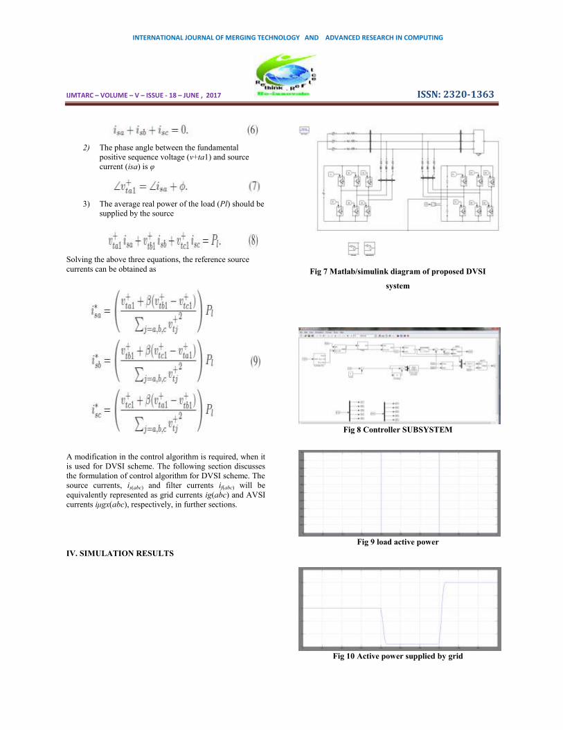
IV. SIMULATION RESULTS
Fig 7 Matlab/simulink diagram of proposed DVSI
system
Fig 8 Controller SUBSYSTEM
Fig 9 load active power
Fig 10 Active power supplied by grid

INTERNATIONAL JOURNAL OF MERGING TECHNOLOGY AND ADVANCED RESEARCH IN COMPUTING
IJMTARC – VOLUME – V – ISSUE - 18 – JUNE , 2017 ISSN: 2320-1363
Fig 11active power supplied by MVSI
Fig 12 active power supplied by AVSI
Fig 13 load currents
Fig 14 grid currents
Fig 15 MVSI currents
Fig 16 AVSI currents
Fig 17 DC Link voltage
V.CONCLUSION
DVSI is Control algorithms are developed to
generate reference currents for DVSI using ISCT. The
proposed scheme has the capability to exchange power
from distributed generators (DGs) and also to compensate
the local unbalanced and nonlinear load. The performance
of the proposed scheme has been validated through
simulation studies. As compared to a single inverter with
multifunctional capabilities, a DVSI has many advantages
such as, increased reliability, lower cost due to the
reduction in filter size, and more utilization of inverter
capacity to inject real power from DGs to microgrid.
Moreover, the use of three-phase, threewire topology for
the main inverter reduces the dc-link voltage requirement.
Thus, a DVSI scheme is a suitable interfacing option for
microgrid supplying sensitive loads. Simulation results are
observed for a proposed fuzzy based DVSI.
REFERENCES
[1] Y. Zhang, N. Gatsis, and G. Giannakis, “Robust energy
management for microgrids with high-penetration
renewables,” IEEE Trans. Sustain.Energy, vol. 4, no. 4, pp.
944–953, Oct. 2013.

INTERNATIONAL JOURNAL OF MERGING TECHNOLOGY AND ADVANCED RESEARCH IN COMPUTING
IJMTARC – VOLUME – V – ISSUE - 18 – JUNE , 2017 ISSN: 2320-1363
[2] R. Majumder, A. Ghosh, G. Ledwich, and F. Zare,
“Load sharing and power quality enhanced operation of a
distributed microgrid,” IETRenewable Power Gener., vol.
3, no. 2, pp. 109–119, Jun. 2009.
[3] J. Guerrero, P. C. Loh, T.-L. Lee, and M. Chandorkar,
“Advanced control architectures for intelligent
microgrids—Part II: Power quality, energy storage, and
ac/dc microgrids,” IEEE Trans. Ind. Electron., vol. 60, no.
4,pp. 1263–1270, Dec. 2013.
[4] Y. Li, D. Vilathgamuwa, and P. C. Loh, “Microgrid
power quality enhancement using a three-phase four-
wiregrid-interfacing compensator,” IEEE Trans. Ind. Appl.,
vol. 41, no. 6, pp. 1707–1719, Nov. 2005.
[5] M. Schonardie, R. Coelho, R. Schweitzer, and D.
Martins, “Control of the active and reactive power using
dq0 transformation in a three-phase grid-connected PV
system,” in Proc. IEEE Int. Symp. Ind. Electron., May
2012, pp. 264–269.
[6] R. S. Bajpai and R. Gupta, “Voltage and power flow
control of grid connected wind generation system using
DSTATCOM,” in Proc. IEEEPower Energy Soc. Gen.
Meeting—Convers. Del. Elect. Energy 21stCentury, Jul.
2008, pp. 1–6.
[7] M. Singh, V. Khadkikar, A. Chandra, and R. Varma,
“Grid interconnection of renewable energy sources at the
distribution level with power-quality improvement
features,” IEEE Trans. Power Del., vol. 26, no. 1, pp. 307–
315, Jan. 2011.
[8] H.-G. Yeh, D. Gayme, and S. Low, “Adaptive VAR
control for distribution circuits with photovoltaic
generators,” IEEE Trans. Power Syst., vol. 27, no. 3, pp.
1656–1663, Aug. 2012.
[9] C. Demoulias, “A new simple analytical method for
calculating the optimum inverter size in grid-connected PV
plants,” Electr. Power Syst.Res., vol. 80, no. 10, pp. 1197–
1204, 2010.
[10] R. Tonkoski, D. Turcotte, and T. H. M. EL-Fouly,
“Impact of high PV penetration on voltage profiles in
residential neighborhoods,” IEEETrans. Sustain. Energy,
vol. 3, no. 3, pp. 518–527, Jul. 2012.
[11] P. Rodriguez et al., “A stationary reference frame grid
synchronization system for three-phase grid-connected
power converters under adverse grid conditions,” IEEE
Trans. Power Electron., vol. 27, no. 1, pp. 99–112, Jan.
2012.
[12] S. Iyer, A. Ghosh, and A. Joshi, “Inverter topologies
for DSTATCOM applications—A simulation study,”
Electr. Power Syst. Res., vol. 75, no. 23, pp. 161–170,
2005.
AUTHOR’S PROFILE:
MANTHENA RAGHUVARANReceived the
B.Tech degree in Electrical & Electronics
Engineering from Holy Mary Institute of Technology
& Science 2015 from JNTU, Hyderabad, Telangana,
India and He is pursuing M.Tech in Electrical Power
System(EPS) as specialization in the Department of
Electrical & Electronics Engineering, SLC’s Institute
of Engineering and Technology, Affiliatedto
theJNTU Hyderabad, Telangana, India. His research
area of interests is Power quality and Renewable
energy sources.
E-mail id:[email protected]
GERA RATNA KUMARI
Completed B.Tech. in Electrical & Electronics
Engineering in 2006 from RVR&JC COLLEGE OF
ENGINEERING, Chowdavaram, GUNTUR Dist,
Affiliated to ANU, Andhra Pradesh, India and
M.Tech in Power systems Engineering in 2010 from
RVR&JC COLLEGEOF ENGINEERING,
Chowdavaram, Guntur, Andhra Pradesh. She is
currently an Assistant Professor with the Department
of Electrical & Electronics Engineering at SLC’S
COLLEGE OF ENGINEERING AND
TECHNOLOGY JNTU, Hyderabad, Telangana,
India. Her area of interest includes Power systems,
design and control of power converters, power
quality, renewable energy sources and FACTS.
E-mail id: [email protected]

INTERNATIONAL JOURNAL OF MERGING TECHNOLOGY AND ADVANCED RESEARCH IN COMPUTING
IJMTARC – VOLUME – V – ISSUE - 18 – JUNE , 2017 ISSN: 2320-1363
Ramavath Shankar
Naikreceived the B.Tech degree in Electrical
Engineering from Vignan’s Engineering College,
Vadlamudi, Guntur, India, in 2006. He Completed
M.E in Electrical Engineering with Power system
Automation as specialization in the Department of
Electrical Engineering, Andhra University College of
Engineering (Autonomous), Visakhapatnam, He is
currently an Associate Professor with the Department
of Electrical &Electronic Engineering at
SLC’sInstitute of Engineering and Technology,
JNTU University, Hyderabad, Telangana, India. His
area of interest lies in Power system operation and
control, optimal operation of power systems and
FACTS.
E-mail id: [email protected]