
Enables 17.5% Binary Organic Solar Cells Electronic ...
20
S1 Electronic Supplementary Information Additive-induced Miscibility Regulation and Hierarchical Morphology Enables 17.5% Binary Organic Solar Cells Jie Lv, ‡ a,b Hua Tang,‡ a,b,c Jiaming Huang, c Cenqi Yan, c Kuan Liu, c Dingqin Hu, a Ranbir Singh, d Jawon Lee, e Shirong Lu, * a Gang Li, * c & Zhipeng Kan * a a. J. Lv, H. Tang, D. Hu, Prof. Z. Kan, Prof. S. Lu, Thin-film Solar Technology Research Center, Chongqing Institute of Green and Intelligent Technology, Chinese Academy of Sciences, Chongqing, 400714, P. R. China. E-mail: [email protected], [email protected] b. J. Lv, H. Tang, University of Chinese Academy of Sciences, Beijing 100049, P. R. China c. H. Tang, Dr. C. Yan, Dr. K. Liu, J. Huang, Prof. G. Li, Department of Electronic and Information Engineering, The Hong Kong Polytechnic University, Hung Hum, Kowloon, Hong Kong SAR, P. R. China. E-mail: [email protected] d. Dr. R. Singh, Department of Energy & Materials Engineering, Dongguk University, Seoul 04620, Republic of Korea e. Dr. J. Lee, Department of Chemical Engineering and Applied Chemistry, Chungnam National University, Daejeon, 34134, Republic of Korea Electronic Supplementary Material (ESI) for Energy & Environmental Science. This journal is © The Royal Society of Chemistry 2018 Electronic Supplementary Material (ESI) for Energy & Environmental Science. This journal is © The Royal Society of Chemistry 2021
Transcript of Enables 17.5% Binary Organic Solar Cells Electronic ...

S1
Electronic Supplementary Information
Additive-induced Miscibility Regulation and Hierarchical Morphology
Enables 17.5% Binary Organic Solar Cells
Jie Lv, ‡a,b Hua Tang,‡a,b,c Jiaming Huang, c Cenqi Yan, c Kuan Liu, c Dingqin Hu, a Ranbir
Singh, d Jawon Lee,e Shirong Lu, * a Gang Li, * c & Zhipeng Kan * a
a. J. Lv, H. Tang, D. Hu, Prof. Z. Kan, Prof. S. Lu, Thin-film Solar Technology Research
Center, Chongqing Institute of Green and Intelligent Technology, Chinese Academy of
Sciences, Chongqing, 400714, P. R. China. E-mail: [email protected],
b. J. Lv, H. Tang, University of Chinese Academy of Sciences, Beijing 100049, P. R. China
c. H. Tang, Dr. C. Yan, Dr. K. Liu, J. Huang, Prof. G. Li, Department of Electronic and
Information Engineering, The Hong Kong Polytechnic University, Hung Hum, Kowloon,
Hong Kong SAR, P. R. China. E-mail: [email protected]
d. Dr. R. Singh, Department of Energy & Materials Engineering, Dongguk University, Seoul
04620, Republic of Korea
e. Dr. J. Lee, Department of Chemical Engineering and Applied Chemistry, Chungnam
National University, Daejeon, 34134, Republic of Korea
Electronic Supplementary Material (ESI) for Energy & Environmental Science. This journal is © The Royal Society of Chemistry 2018Electronic Supplementary Material (ESI) for Energy & Environmental Science.This journal is © The Royal Society of Chemistry 2021
S2
Content
1. Device Fabrication ..........................................................................................3
2. Additional PV Device Performance Data .....................................................4
4. Contact angle measurements .........................................................................5
5. Transfer Matrix calculation...........................................................................8
6. UV-Vis Absorption .......................................................................................11
7. Grazing Incidence Wide-angle X-ray Scattering.......................................12
8. Atomic Force Microscopy (AFM) Imaging ................................................14
9. Transmission Electron Microscopy (TEM) Characterization..................15
10. J-V curves with varied incident light intensity.........................................16
11. Transient photovoltage (TPV) and transient photocurrent (TPC)........16
12. SCLC Measurements..................................................................................17
13. The PCE distribution .................................................................................19
14. reference ......................................................................................................20

S3
1. Device Fabrication
The PM6:Y6 organic solar cells were prepared on glass substrates with tin-doped indium
oxide (ITO, 15 Ω/sq) patterned on the surface (device area: 0.1 cm2). Substrates were
prewashed with isopropanol to remove organic residues before immersing in an ultrasonic bath
of soap for 15 min. Samples were rinsed in flowing deionized water for 5 min before being
sonicated for 15 min each in successive baths of deionized water, acetone and isopropanol.
Next, the samples were dried with pressurized nitrogen before being exposed to a UV-ozone
plasma for 15 min. PEDOT:PSS was diluted with the same volume of water, a thin layer of
PEDOT:PSS (~20 nm) (Clevios AL4083) was spin-coated onto the UV-treated substrates, the
PEDOT-coated substrates were subsequently annealed on a hot plate at 160 °C for 15 min, and
the substrates were then transferred into the glovebox for active layer deposition.
All solutions were prepared in the glovebox using the donors of PM6 and the acceptor of
Y6; The PM6 and Y6 were purchased from organtec.ltd., and the1-fluoronaphthalene(FN), 1-
chloronaphthalene(CN) and 1-bromonaphthalene(BN) were purchased from Shanghai Titan
Technology Co. , Ltd.. Optimized devices were obtained by dissolving PM6 and Y6 in
chloroform (CF) using a D/A ratio of 1:1.2, 1:1.2 with 0.9% FN, 1:1.2 with 0.5% CN and 1:1.2
with 0.6% BN (vol/vol), total concentration of 16 mg/ml. Note: The as-prepared solutions were
stirred overnight at room temperature before being spin coat on the PEDOT:PSS substrates.
The active layers were spin-coated at an optimized speed of 3000 rpm for time period of 30s,
resulting in films of 110 to 120 nm in thickness. The active layers were then thermal annealing
(TA) for 10 min at 110 °C.
The next stage is to coat ETL on active layer, about 50 uL PFNBr solution (0.5 mg/ml in
Methanol) was spin-coated at 3000 rpm for 20s. Finally, the samples were placed in a thermal
evaporator for evaporation of a 90 nm-thick layer of Silver (Ag) evaporated at 2 Å s−1; pressure
of less than 2x10⁻⁶ Torr. Following electrode deposition, samples underwent J−V testing.
The current density-voltage (J-V) curves of devices were measured using a Keithley 2400
Source Meter in glove box under AM 1.5G (100 mW cm-2) using a Enlitech solar simulator
(purchased from Enli Technology Co., Ltd.). A 2×2 cm2 monocrystalline silicon reference
cell with KG1 filter (purchased from Enli Tech. Co., Ltd., Taiwan). The external quantum
efficiency (EQE) was measured by a certified incident photon to electron conversion (IPCE)
equipment (QE-R) from Enli Technology Co., Lt. The light intensity at each wavelength
was calibrated using a standard monocrystalline Si photovoltaic cell.

S4
2. PV Device Performance Data
Table S1. Summary of PV performance for PM6:Y6-based OSCs with different volume ratio
of FN in conventional devices under AM 1.5G 100 mW/cm2 illumination.
Materials Condition VOC [V] JSC [mA cm-2] FF [%] PCE [%]
0.5%FN 0.85 25.54 70.7 15.20.6%FN 0.84 26.06 70.6 15.40.7%FN 0.83 26.52 72.6 16.10.8%FN 0.83 26.79 74.4 16.60.9%FN 0.83 26.98 77.8 17.5
PM6:Y61:1.2
1% FN 0.83 26.03 75.9 16.5
Table S2. Summary of PV performance for PM6:Y6-based OSCs with different volume ratio
of BN in conventional devices under AM 1.5G 100 mW/cm2 illumination.
Materials Condition VOC [V] JSC [mA cm-2] FF [%] PCE [%]
0.3%BN 0.83 25.13 72.2 15.20.4%BN 0.83 25.84 71.6 15.50.5%BN 0.83 25.96 73.4 15.90.6%BN 0.84 26.00 74.9 16.40.7%BN 0.84 26.08 73.4 16.1
PM6:Y61:1.2
0.8%BN 0.83 24.90 74.2 15.3
Table S3. Summary of PV performance for PM6:Y6-based OSCs with different additives in
conventional devices under AM 1.5G 100 mW/cm2 illumination. All of cells performed without
any treatment.
Materials Condition VOC [V] JSC [mA cm-2] FF [%] PCE [%]
0.9%FN 0.86 25.70 72.7 16.10.5%CN 0.87 23.89 73.0 15.1PM6:Y6
1:1.20.6%BN 0.88 22.56 74.8 14.9

S5
4. Contact angle measurements
Table S4. Summarized Contact Angles of the materials.
Contact Angle (deg)Films
a) H2O b) formamide,FA
106.90 82.20106.70 82.60PM6106.83 81.90
106.30 85.70 106.40 85.30 PM6 FN106.42 85.80
106.30 84.80 106.20 84.70 PM6 CN106.40 84.72
106.00 86.70 105.80 86.60 PM6 BN105.90 86.40
93.20 71.70 93.60 71.80 Y693.00 72.00
95.10 76.30 95.20 76.20 Y6 FN95.18 76.70
93.60 71.00 93.40 70.70 Y6 CN93.30 70.60
94.80 78.90 95.10 78.40 Y6 BN95.20 78.70
a) Deionized water; b) formamide;

S6
Table S5. Summarized Average Contact Angles and Surface FreeEnergy Parameters of the
materials
Contact Angle (deg)Films
a) H2O b) formamide,FAsurface free energy,γ (mJ m-2)
PM6 106.81(±0.09) 82.23(±0.37) 25.36
PM6 FN 106.37(±0.20) 85.60(±0.03) 20.64
PM6 CN 106.30(±0.10) 84.74(±0.06) 21.62
PM6 BN 105.90(±0.10) 86.57(±0.13) 19.22
Y6 93.27(±0.33) 71.83(±0.17) 27.58
Y6 FN 95.16(±0.04) 76.40(±0.30) 23.76
Y6 CN 93.43(±0.17) 70.77(±0.23) 28.93
Y6 BN 95.03(±0.17) 78.67(±0.23) 21.57
a) Deionized water; b) formamide;
The contact angles of the films were performed on a DSA-100 (KRUSS Germany) contact angle
meter. Then the surface free energy was calculated by Owens-Wendt method:1, 2
(1)𝛾𝐿 × (1 + cos 𝜃) = 2 × (𝛾𝑑𝐿 ∙ 𝛾 𝑑
𝑠𝑣)1 2 + 2 × (𝛾𝑝𝐿 ∙ 𝛾 𝑝
𝑠𝑣)1 2
where and γS are surface free energy of the probe liquid and sample, respectively, θ is the contact 𝛾𝐿
angle of the sample.
The average contact angles of two liquids (deionized water and formamide) on the various
neat films were measured and the results (Test three times separately) in Table S4, and the
average contact angles and surface energy parameters are summarized in Table S5. Then
calculate the Flory-Huggins interaction parameter χdonor−acceptor for blend to show the binary
miscibility from

S7
(2)𝐾(𝛾 1 2𝑑𝑜𝑛𝑜𝑟 ‒ 𝛾 1 2
𝑎𝑐𝑐𝑒𝑝𝑡𝑜𝑟)2
where γ is the surface energy of the material, K is the proportionality constant. 3, 4
θ=106.81°
NA FN CN BN
H2O
FA
θ=82.23°
θ=106.37°
θ=85.60°
θ=106.30°
θ=84.74°
θ=105.90°
θ=86.57°
Figure S1. The Deionized water and formamide (FA) contact angles of the pristine PM6 of
NA ,FN, CN and BN.
H2O
FA
θ=93.27°
θ=71.83°
θ=95.16°
θ=76.40°
θ=93.43°
θ=70.70°
θ=95.03°
θ=78.67°
NA FN CN BN
Figure S2. The Deionized water and formamide (FA) contact angles of the pristine Y6 of NA
,FN, CN and BN.

S8
5. Transfer Matrix calculation
0 100 200 300 400 500 6000
5
10
15
20
25
30
J SC (m
Acm
-2)
Thickness (nm)
PM6:Y6
(a)
Figure S3. (a) Maximum theoretical JSC plots vs. active layer thickness; curves simulated via
transfer matrix for optimized blends of PM6:Y6. The model assumes 100% IQE.
Transfer matrix modeling was used to simulate the maximum theoretical JSC plots as a
function of active layer thickness (thickness range: 0-600 nm) for optimized blends of PM6:Y6;
the model assumes 100% internal quantum efficiency (IQE). The transfer matrix code for these
simulations was developed by George F. Burkhard and Eric T. Hoke; code available from:
http://web.stanford.edu/group/ mcgehee/transfermatrix/index.html.5, 6 The optical constants n
and k for the active layers described in Figure S4 and Figure S5.

S9
(a)
Figure S4. (a) The PM6:Y6 blend film variable angle spectrospotic ellipsornetric (VASE) data
and the fittings.
Notes on Ellipsometry (EM) measurements and data analysis:
The films were prepared on optical glasses following the active layer conditions and tested
with the M-2000 Ellipsometer. The measured data were fitted with the software
CompleteEASE with Gen-Osc models. The fitting quality was evaluated by the MSE values,
and MSE values of 2.676 was obtained for the thin film fitting. The thickness value ca. 106 nm
was obtained from the fitting, in line with the experimental data. The experimental data were
well fitted by the models applied as shown in Figure S4.

S10
200 400 600 800 1000120014001600
0.0
0.5
1.0
1.5
2.0
2.5
3.0
0.0
0.5
1.0
1.5
2.0
2.5
3.0
k
Wavelength (nm)
n
(a)
Figure S5. n and k values fitted from the ellipsometry measurements.

S11
6. UV-Vis AbsorptionUV-vis absorption spectra of PM6:Y6 different additives under thermal annealing were recorded on a PerkinElmer LAMBDA 365 UV-Vis spectrophotometer.
Figure S6. UV-vis absorbance spectra of PM6:Y6 with (a) NA, (b) FN, (c) CN and (d) BN under thermal annealing (TA) of 0 and 45s, (e) UV-vis absorbance spectra of PM6:Y6 (after TA for 0s and 45 s) processed with NA, FN, CN, and BN.

S12
7. Grazing Incidence Wide-angle X-ray Scattering
Grazing-incidence wide-angle X-ray scattering (GIWAXS) was measured at Pohang Light
Source (Korea), beam line 3C. Silicon substrates for GIWAXS test were sonicated for 15 min
each in successive baths of detergent, DI water, acetone and isopropanol. The substrates were
then dried with pressurized nitrogen before being exposed to the UV−ozone plasma for 20 min.
The BHJ layers were prepared following methods described in Section of Device Fabrication.
NA FN CN BN(a) (b) (c) (d)
BNCNFNNA(e) (f) (g) (h)
Figure S7. 2D GIWAX patterns of pristine films based on PM6 of (a) NA, (b) FN, (c) CN, (d)
BN; 2D GIWAX patterns of pristine films based on Y6 of (e) NA, (f) FN, (g) CN, (h) BN;
0.5 1.0 1.5 2.0 2.5
NA
FN
CN
BN
Inte
nsity
(a.u
.)
Out-of-Plane
qz (Å-1)1
BN
CN
FN
NA
0.30.2 0.6
Inte
nsity
(a.u
.)
In-Plane
qxy (Å-1)
(a) (b)
Figure S8. (a) Corresponding GIWAXS intensity profiles along the out-of-plane directions of
PM6: Y6 blend films of NA, FN, CN and BN; And (b) corresponding GIWAXS intensity
profiles along the in-plane directions of PM6: Y6 blend films of NA, FN, CN and BN.
S13
In-plane Out-of-plane PM6 PM6
NA
FNCNBN
NAFNCNBN
(a) (b)
Out-of-plane In-plane Y6 Y6
NA
FNCNBN
NA
FN
CN
BN
(c) (d)
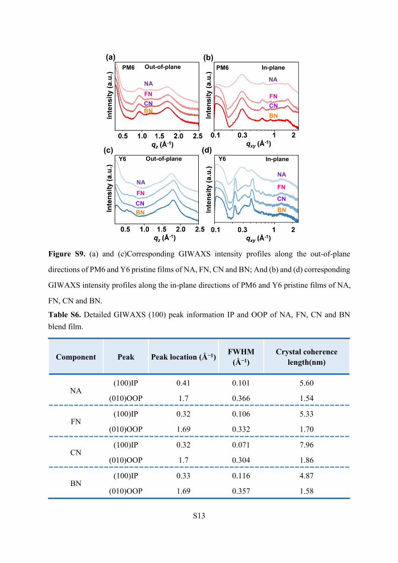
Figure S9. (a) and (c)Corresponding GIWAXS intensity profiles along the out-of-plane
directions of PM6 and Y6 pristine films of NA, FN, CN and BN; And (b) and (d) corresponding
GIWAXS intensity profiles along the in-plane directions of PM6 and Y6 pristine films of NA,
FN, CN and BN.
Table S6. Detailed GIWAXS (100) peak information IP and OOP of NA, FN, CN and BN blend film.
Component Peak Peak location (Å−1) FWHM (Å−1)
Crystal coherence length(nm)
(100)IP 0.41 0.101 5.60NA
(010)OOP 1.7 0.366 1.54
(100)IP 0.32 0.106 5.33FN
(010)OOP 1.69 0.332 1.70
(100)IP 0.32 0.071 7.96CN
(010)OOP 1.7 0.304 1.86
(100)IP 0.33 0.116 4.87BN
(010)OOP 1.69 0.357 1.58

S14
8. Atomic Force Microscopy (AFM) Imaging
Topographic images of the films were obtained from a Bruker atomic force microscopy (AFM)
with the type of dimension edge with Scan AsystTM in the tapping mode using an etched
silicon cantilever at a nominal load of ~2nN, the scanning rate for a 2 μm×2 μm image size
was 0.9 Hz and 5 μm×5 μm image size was 1.0 Hz.
NA
phase
Rq=0.80 nmFN
phase
Rq=0.81 nmCN
phase
Rq=0.83 nmBN
phase
Rq=0.88 nm(a) (b) (c) (d)
Figure S10. AFM height images with phase images inset of PM6 pristine film of (a) NA, (b) FN, (c) CN, (d) BN.
NA(a) Rq=1.29 nm
(e)
FNRq=2.52 nm
CNRq=1.44 nm
(b) (c) BNRq=1.95 nm(d)
(f) (g) (h)
(j) (k) (l) (i)
Figure S11. AFM height images of Y6 pristine film of (a) NA, (b) FN, (c) CN, (d) BN, and AFM phase images of Y6 pristine film of (e) NA, (f) FN, (g) CN and (h) BN; Corresponding Three-dimensional (3D) AFM surface roughness images of Y6 pristine film of (i) NA, (j) FN, (k) CN and (l) BN.

S15
9. Transmission Electron Microscopy (TEM) Characterization
Films were spun-cast on PEDOT:PSS-coated glass substrates. The PM6, Y6 and BHJ films
were floated off the substrates in deionized water and collected on lacey carbon coated TEM
grids (Electron Microscopy Sciences). TEM studies were performed a Thermo Fischer (former
FEI) Titan 80-300 TEM equipped with an electron monochromator and a Gatan Imaging Filter
(GIF) Quantum 966.
(a) (d) (b) (c) NA FN CN BN
Figure S12. TEM images of PM6:Y6 blend film of (a) NA, (b) FN, (c) CN, (d) BN.
NA FN CN BN(a) (b) (c) (d)
FN CN BN(e) (f) (g) (h) NA
Figure S13. TEM images of PM6 pristine film of (a) NA, (b) FN, (c) CN, (d) BN and TEM
images of Y6 pristine film of (e) NA, (f) FN, (g) CN and (h) BN;

S16
10. J-V curves with varied incident light intensity
-1.0 -0.5 0.0 0.5 1.0 1.5
-25
-20
-15
-10
-5
0
5
1 0.84 0.75 0.65 0.55 0.44 0.34 0.23 0.14 0.09 0.05 0.03
Voltage (Volt)
J (m
Ac
m-2
)PM6:Y6 NA
-1.0 -0.5 0.0 0.5 1.0 1.5-30
-25
-20
-15
-10
-5
0
5
1 0.84 0.75 0.65 0.55 0.44 0.34 0.23 0.14 0.09 0.05 0.03
Voltage (Volt)
J (m
Ac
m-2
)
PM6:Y6 FN
-1.0 -0.5 0.0 0.5 1.0 1.5
-25
-20
-15
-10
-5
0
5
1 0.84 0.75 0.65 0.55 0.44 0.34 0.23 0.14 0.09 0.05 0.03
Voltage (Volt)
J (m
Ac
m-2
)
PM6:Y6 CN
0.0 0.5 1.0
-25
-20
-15
-10
-5
0
5
1 0.84 0.75 0.65 0.55 0.44 0.34 0.23 0.14 0.09 0.05 0.03
Voltage (Volt)
J (m
Ac
m-2
)PM6:Y6 BN
(a) (b)
(c) (d)
Figure S14. J-V curves with various incident light intensities of (a) NA, (b) FN, (c) CN and
(d) BN devices.
11. Transient photovoltage (TPV) and transient photocurrent (TPC)
For TPV, the measurement was conducted under 1 sun conditions by illuminating the
device with a white light-emitting diode, and the champion device is set to the open-circuit
condition. For TPC, the champion device is set to the short-circuit condition in dark. The output
signal was collected by keysight oscilloscope.

S17
60 80 100
0.839
0.840
0.841
0.842
0.843
0.844
0.845
0.846
Time (s)
TPV(
V)NA
FN
CN
BN
0 5 10 15 20
0.001
0.002
0.003
0.004
0.005
0.006
0.007
0.008
NA FN CN BN
Time (s)
TPC
(A)
(a) (b)
Figure S15. (a) TPV and (b) TPC of the PM6: Y6 devices processed with NA, FN, CN, and
BN.
12. SCLC Measurements
Fitting the hole/electron-only diode dark current to the space charge limited current
(SCLC) model can obtain the hole and electron mobility of the photosensitive active layer.The
electron-only device structure was ITO/ZnO/ PFNBr/ BHJ/ PFNBr /Ag, and the hole-only
device structure was ITO/PEDOT:PSS/BHJ/MoO3/Ag. Using the following equation to
estimate the electric-field dependent SCLC mobility:
(3)𝐽(𝑉) =
98
𝜀0𝜀𝑟𝜇0𝑒𝑥𝑝(0.89𝛽𝑉 ‒ 𝑉𝑏𝑖
𝐿 )(𝑉 ‒ 𝑉𝑏𝑖)2
𝐿3
For the hole-only device structure, Vbi = 0 V (flat band pattern formed by PEDOT:PSS-
MoO3); For the electron-only device structure, Vbi = 0.5 V was used following the protocol
reported.

S18
0 1 2 3 4 510-3
10-2
10-1
100
101
102
103
104
Hole 4.08× 10⁻⁴ cm2V-1S-1
Hole 5.24× 10⁻⁴ cm2V-1S-1
Hole 7.34× 10⁻⁴ cm2V-1S-1
Hole 4.66× 10⁻⁴ cm2V-1S-1
Cur
rent
den
sity
(mA
/cm
2 )
Voltage (V)
NA FN CN BN
0 1 2 3 4 510-4
10-3
10-2
10-1
100
101
102
103
104
elctron 2.63× 10⁻⁴ cm2V-1S-1
elctron 5.28× 10⁻⁴ cm2V-1S-1
elctron 5.55× 10⁻⁴ cm2V-1S-1
elctron 4.46× 10⁻⁴ cm2V-1S-1
Cur
rent
den
sity
(mA
/cm
2 )
Voltage (V)
NA FN CN BN
(a) (b)
Figure S16. Dark J–V curves of the NA, FN, CN, BN OSCs: (a) electron-only diodes and (b)
hole-only diodes; The solid lines are fit to the experimental data according to the equation (3).
Table S7. Summary of carrier mobilities
Active layer μh [×10-4 cm2 V−1 s−1] μe [×10-4 cm2 V−1 s−1] μh /μe
Non-additive 4.08±0.11 2.63±0.31 1.55
FN 5.24±0.14 5.28±0.19 0.99
CN 7.34±0.43 5.55±0.31 1.38
BN 4.66±0.30 4.46±0.11 1.04

S19
13. Device statistics
Figure S17. The PCE statistics of PM6:Y6 with NA, FN, CN and BN.

S20
14. reference
1. M.-C. Michalski, J. Hardy and B. J. V. Saramago, J. Colloid Interface Sci., 1998, 208,
319-328.
2. D. K. Owens and R. C. Wendt, J. Appl. Polym. Sci., 1969, 13, 1741-1747.
3. Z. Cao, J. Chen, S. Liu, M. Qin, T. Jia, J. Zhao, Q. Li, L. Ying, Y.-P. Cai, X. Lu, F. Huang
and Y. Cao, Chem. Mater., 2019, 31, 8533-8542.
4. S. Pang, R. Zhang, C. Duan, S. Zhang, X. Gu, X. Liu, F. Huang and Y. Cao, Adv. Energy
Mater., 2019, 9, 1901740.
5. Y. Firdaus, L. P. Maffei, F. Cruciani, M. A. Müller, S. Liu, S. Lopatin, N. Wehbe, G. O. N.
Ndjawa, A. Amassian, F. Laquai and P. M. Beaujuge, Adv. Energy Mater., 2017, 7,
1700834.
6. J. Wu, G. Li, J. Fang, X. Guo, L. Zhu, B. Guo, Y. Wang, G. Zhang, L. Arunagiri, F. Liu, H.
Yan, M. Zhang and Y. Li, Nat. Commun., 2020, 11, 4612.


![SRUCTURAL HARDENING MECHANISM OF LEAD-CADMIUM … · The binary system Pb-Cd alloy [3] (Fig. 1) represents a eutectic at 248 ° C. The eutectic liquid composition is about 17.5% by](https://static.fdocuments.us/doc/165x107/5e34126b5e842941434f3beb/sructural-hardening-mechanism-of-lead-cadmium-the-binary-system-pb-cd-alloy-3.jpg)