EMC Basics concepts
25
EMC Basics concepts
-
Upload
hillary-goff -
Category
Documents
-
view
76 -
download
3
description
EMC Basics concepts. Summary. Basic Principles Specific Units LC Resonance Radiating element Emission Spectrum Susceptibility Spectrum Notion of margin Impedance Conclusion. Basic principles. CONDUCTED AND RADIATED EMI. Conducted mode. Radiated mode. - PowerPoint PPT Presentation
Transcript of EMC Basics concepts
EMC Basics concepts
2 19 Apr 2023
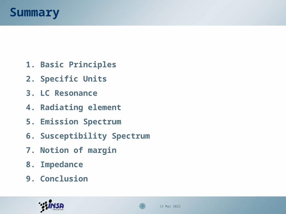
1. Basic Principles
2. Specific Units
3. LC Resonance
4. Radiating element
5. Emission Spectrum
6. Susceptibility Spectrum
7. Notion of margin
8. Impedance
9. Conclusion
Summary
3 19 Apr 2023
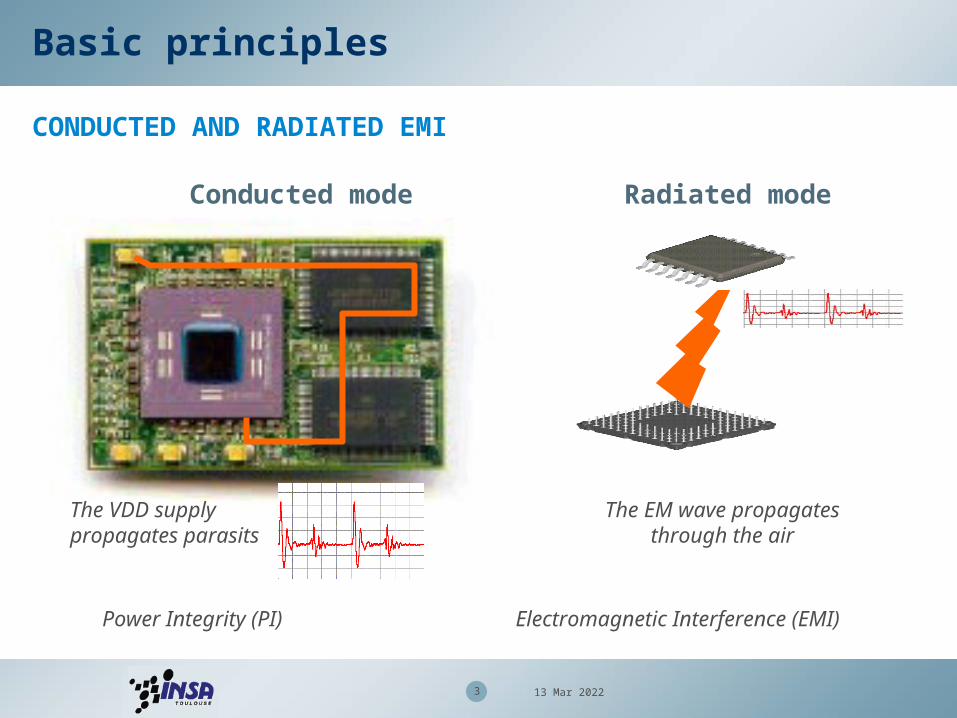
Radiated mode
The VDD supply propagates parasits
The EM wave propagates through the air
Basic principles
CONDUCTED AND RADIATED EMI
Conducted mode
Power Integrity (PI) Electromagnetic Interference (EMI)
4 19 Apr 2023
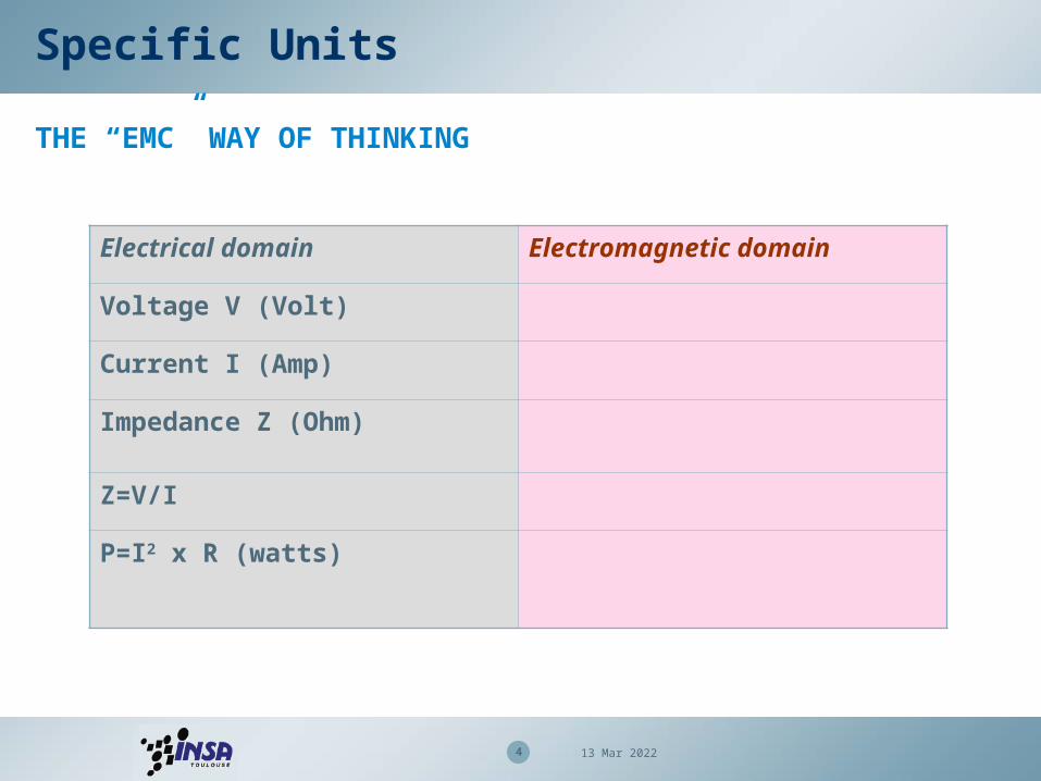
Electrical domain Electromagnetic domain
Voltage V (Volt)
Current I (Amp)
Impedance Z (Ohm)
Z=V/I
P=I2 x R (watts)
Specific Units
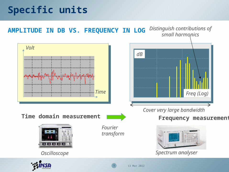
THE “EMC” WAY OF THINKING
5 19 Apr 2023
Time domain measurement
Volt
Time
Specific units
AMPLITUDE IN DB VS. FREQUENCY IN LOG
Oscilloscope
Frequency measurement
Fourier transform
Freq (Log)
dB
Spectrum analyser
Distinguish contributions of small harmonics
Cover very large bandwidth
6 19 Apr 2023
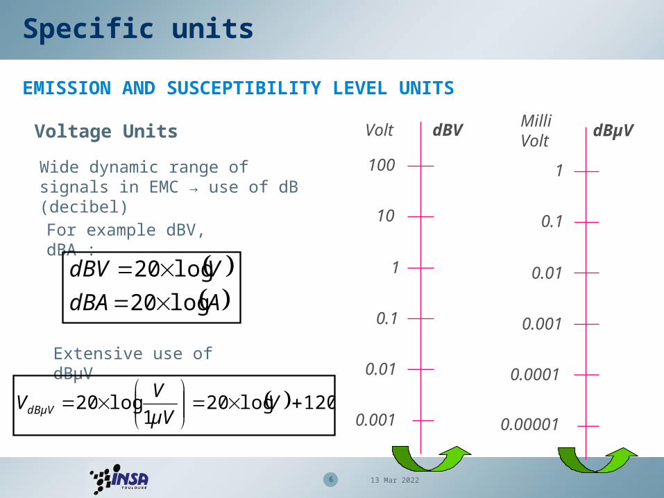
Voltage Units
Wide dynamic range of signals in EMC → use of dB (decibel)
0.1
10
1
100
0.01
Volt dBV
0.001
0.001
0.1
0.01
1
0.0001
MilliVolt
dBµV
0.00001
Specific units
EMISSION AND SUSCEPTIBILITY LEVEL UNITS
For example dBV, dBA :
AdBA
VdBV
log20
log20
Extensive use of dBµV
120log201
log20
V
µV
VVdBµV
7 19 Apr 2023
The most common power unit is the “dBm” (dB milli-Watt)
Power Units
1 mV = ___ dBµV
1 W = ___ dBm
Exercise: Specific units
Specific units
EMISSION AND SUSCEPTIBILITY LEVEL UNITS
30log101
log10
W
WdBmW P
mW
PP
1 W
1 MW
1 KW
Power(Watt)
1 mW
Power(dBm)
1 µW
1 nWIC-EMC: 0dbm in 50
Tools > dB/Unit converter
IC-EMC: 0dbm in 50
Tools > dB/Unit converter
8
LC Resonance
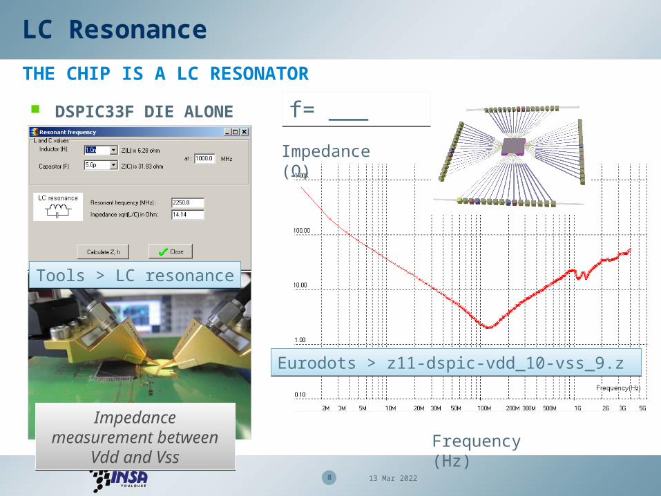
THE CHIP IS A LC RESONATOR
DSPIC33F DIE ALONE
Impedance measurement between Vdd and Vss
Impedance measurement between Vdd and Vss
Impedance (Ω)
Frequency (Hz)
Eurodots > z11-dspic-vdd_10-vss_9.z Eurodots > z11-dspic-vdd_10-vss_9.z
Tools > LC resonanceTools > LC resonance
f= ___f= ___
19 Apr 2023
9
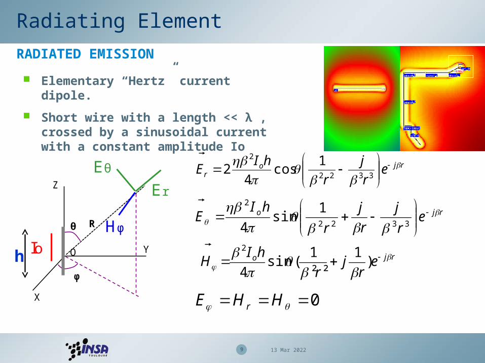
Radiating Element
RADIATED EMISSION
Y
Z
O
φ
θ R
X
Eθ
Hφ
Er
Io
rjor e
r
j
r
hIE
3322
2 1cos
42
rjo er
j
r
j
r
hIE
3322
2 1sin
4
rjo er
jr
hIH
)
1
²²
1(sin
4
2
0
HHE r
h
Elementary “Hertz” current dipole.
Short wire with a length << λ , crossed by a sinusoidal current with a constant amplitude Io
19 Apr 2023
10 19 Apr 2023
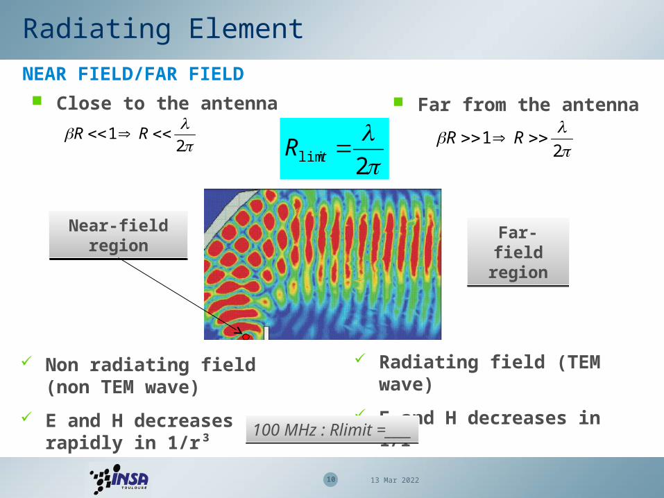
Radiating Element
NEAR FIELD/FAR FIELD
21 RR
21 RR
Close to the antenna Far from the antenna
2lim itR
Non radiating field (non TEM wave)
E and H decreases rapidly in 1/r³
Radiating field (TEM wave)
E and H decreases in 1/r
Near-field region
Near-field region
Far-field region
Far-field region
100 MHz : Rlimit =____100 MHz : Rlimit =____
11 19 Apr 2023
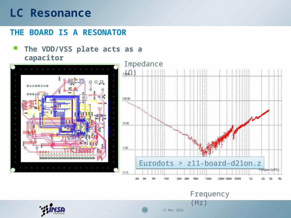
LC Resonance
THE BOARD IS A RESONATOR
The VDD/VSS plate acts as a capacitor
Impedance (Ω)
Frequency (Hz)
Eurodots > z11-board-d21on.zEurodots > z11-board-d21on.z
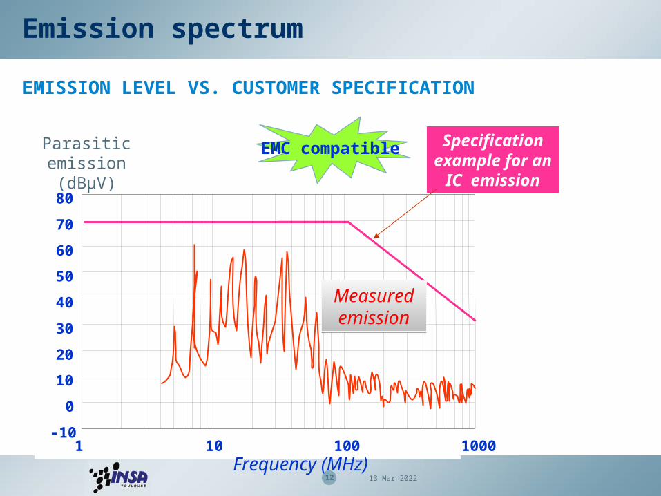
12 19 Apr 2023
Specification example for an IC
emission
Parasitic emission (dBµV)
-10
0
10
20
30
40
50
60
70
80
1 10 100 1000Frequency (MHz)
Measured emissionMeasured emission
EMC compatible
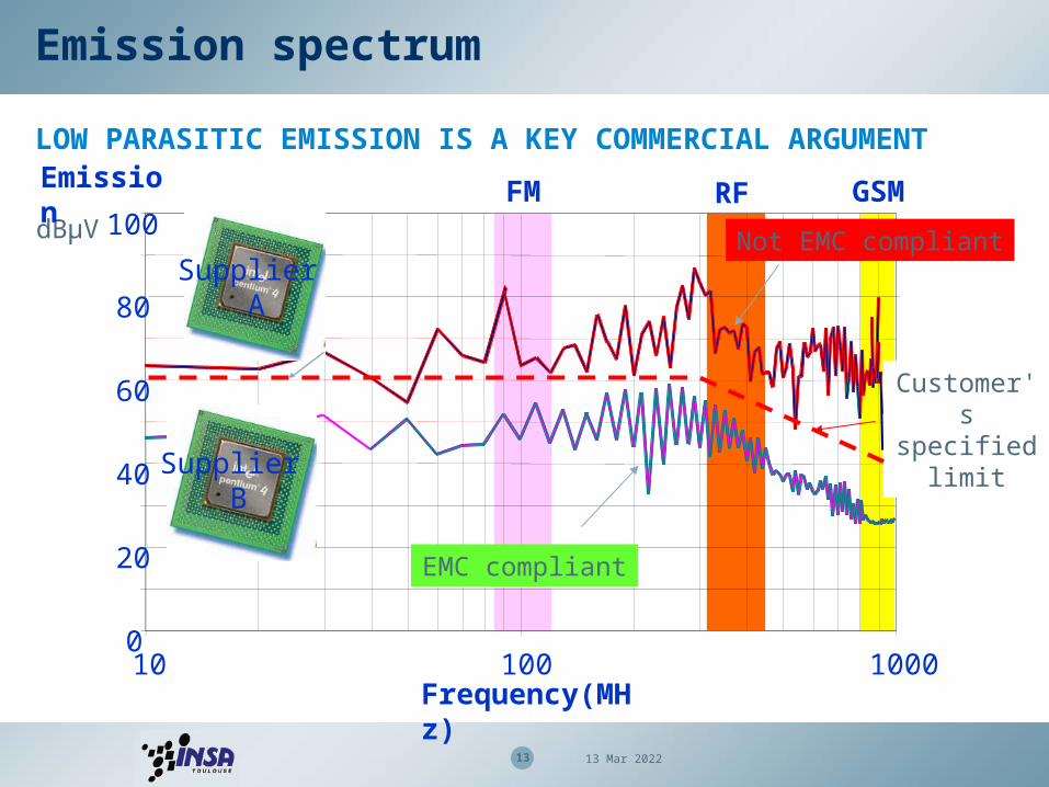
Emission spectrum
EMISSION LEVEL VS. CUSTOMER SPECIFICATION
13 19 Apr 2023
dBµV
0
20
40
60
80
100
10 100 1000
FM GSMRF
Supplier A
Supplier B
EMC compliant
Not EMC compliant
Frequency(MHz)
Customer's specified
limit
Emission spectrum
LOW PARASITIC EMISSION IS A KEY COMMERCIAL ARGUMENTEmission
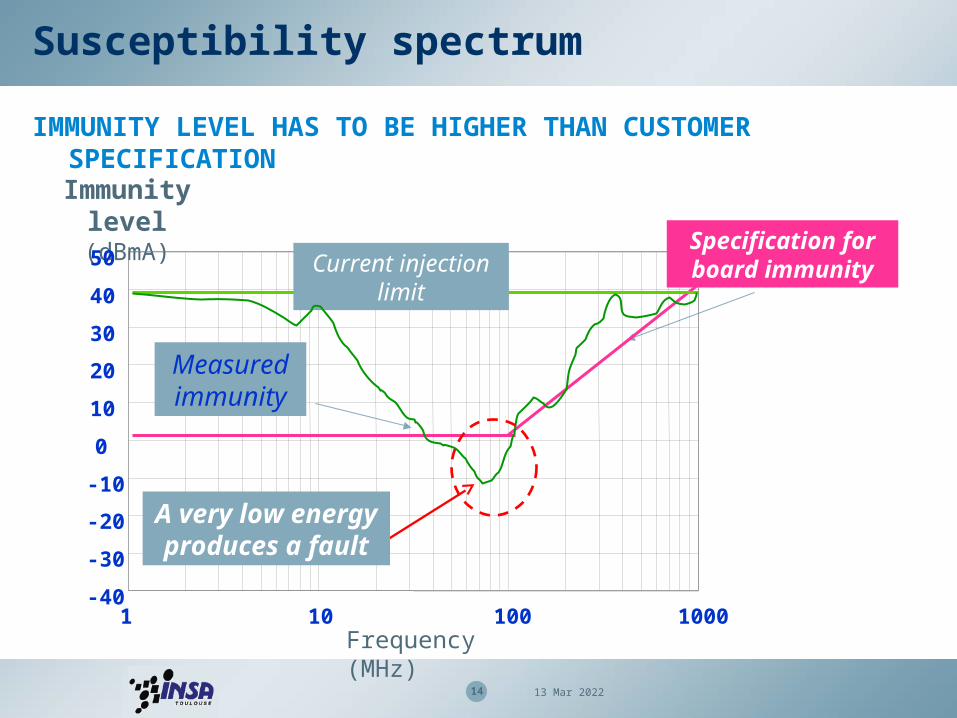
Susceptibility spectrum
14 19 Apr 2023
Immunity level (dBmA)
-40
-30
-20
-10
0
10
20
30
40
50
1 10 100 1000
Specification for board immunityCurrent injection limit
Measured immunity
A very low energy produces a fault
Frequency (MHz)
IMMUNITY LEVEL HAS TO BE HIGHER THAN CUSTOMER SPECIFICATION
15 19 Apr 2023
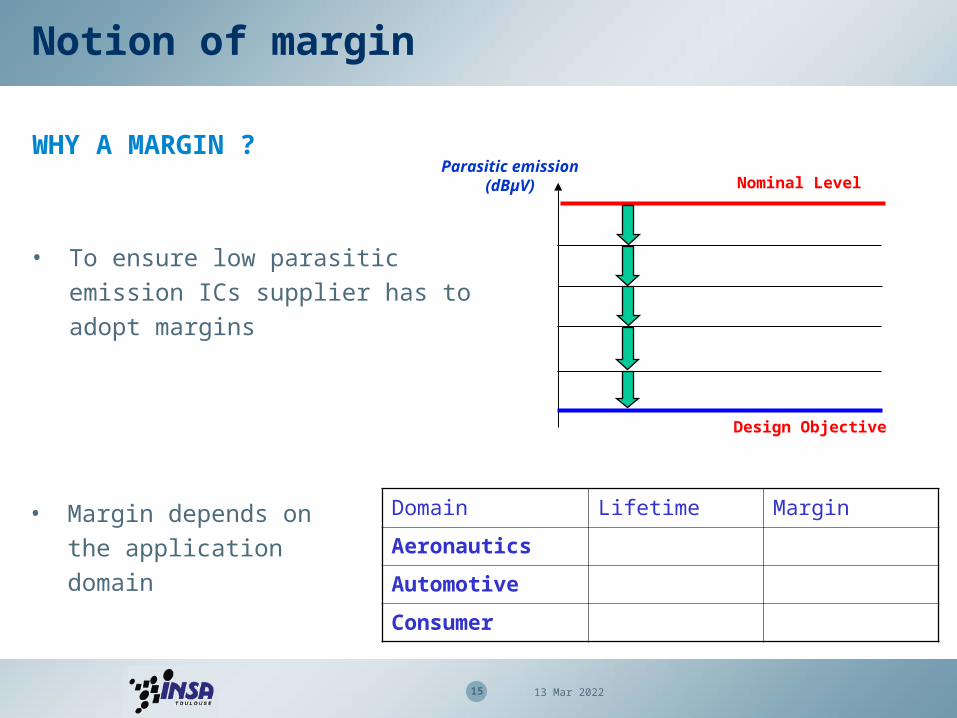
Notion of margin
WHY A MARGIN ?
Domain Lifetime Margin
Aeronautics
Automotive
Consumer
Parasitic emission (dBµV)Nominal Level
Design Objective
• To ensure low parasitic emission ICs
supplier has to adopt margins
• Margin depends on the
application domain
16 19 Apr 2023
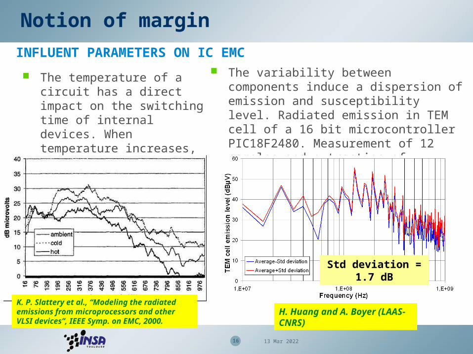
INFLUENT PARAMETERS ON IC EMC
The temperature of a circuit has a direct impact on the switching time of internal devices. When temperature increases, the high frequency content of the emission spectrum tends to be reduced.
K. P. Slattery et al., “Modeling the radiated emissions from microprocessors and other VLSI devices”, IEEE Symp. on EMC, 2000.
Notion of margin
The variability between components induce a dispersion of emission and susceptibility level. Radiated emission in TEM cell of a 16 bit microcontroller PIC18F2480. Measurement of 12 samples and extraction of emission level dispersion.
H. Huang and A. Boyer (LAAS-CNRS)
Std deviation = 1.7 dB
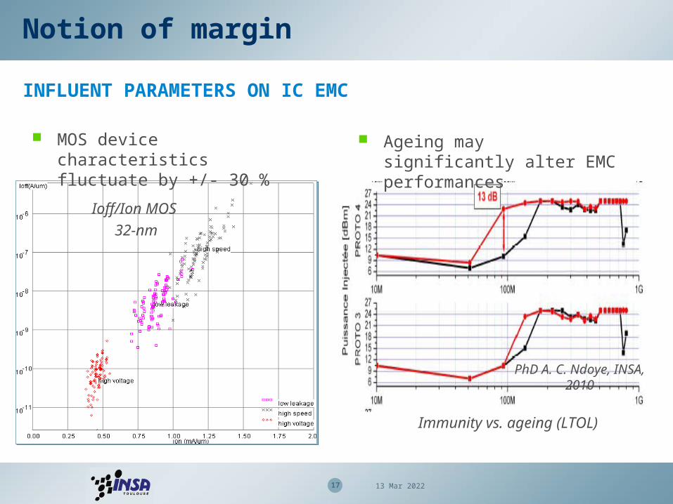
17 19 Apr 2023
Ioff/Ion MOS 32-nm
PhD A. C. Ndoye, INSA, 2010
Immunity vs. ageing (LTOL)
Notion of margin
INFLUENT PARAMETERS ON IC EMC
MOS device characteristics fluctuate by +/- 30 %
Ageing may significantly alter EMC performances
18 19 Apr 2023
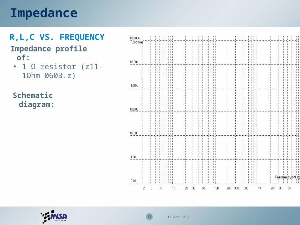
R,L,C VS. FREQUENCY
Impedance profile of:
Impedance
• 1 Ω resistor (z11-1Ohm_0603.z)
Schematic diagram:
19 19 Apr 2023
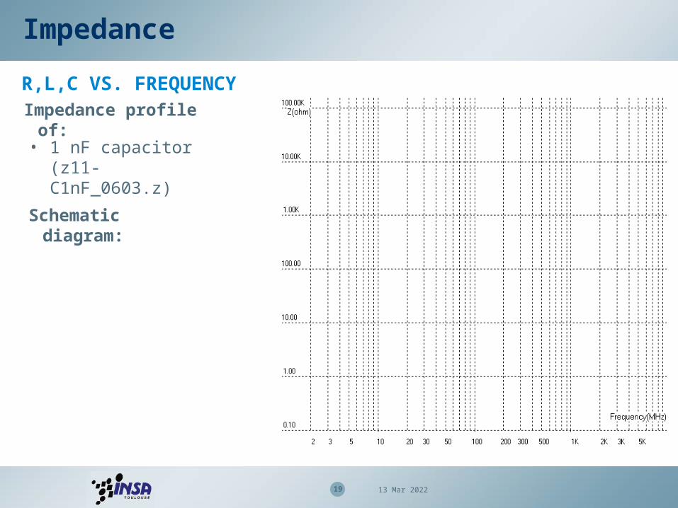
R,L,C VS. FREQUENCY
Impedance
• 1 nF capacitor (z11-C1nF_0603.z)
Impedance profile of:
Schematic diagram:
20 19 Apr 2023
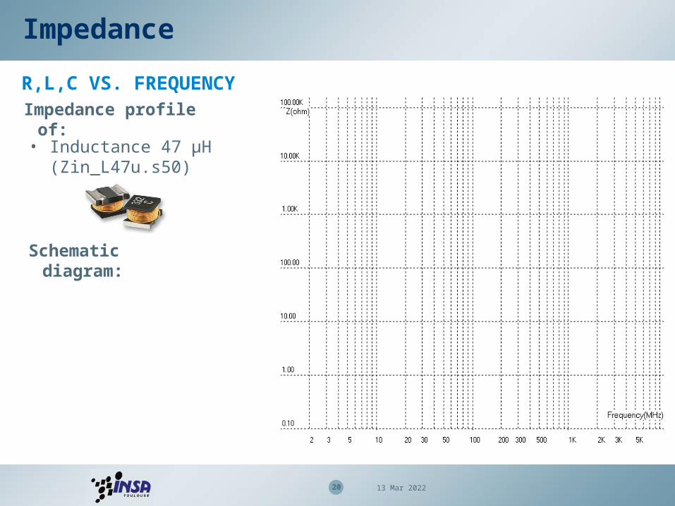
R,L,C VS. FREQUENCY
Impedance
• Inductance 47 µH (Zin_L47u.s50)
Impedance profile of:
Schematic diagram:
21 19 Apr 2023
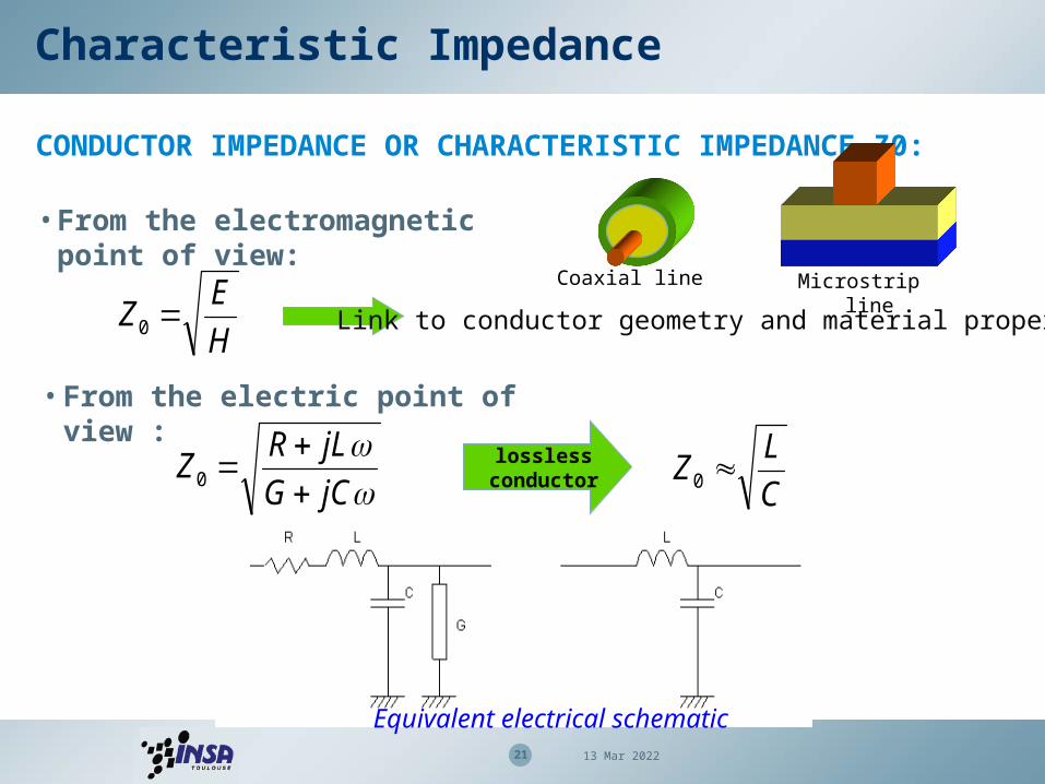
CONDUCTOR IMPEDANCE OR CHARACTERISTIC IMPEDANCE Z0:
Characteristic Impedance
Coaxial line Microstrip line
• From the electromagnetic point of view:
H
EZ 0 Link to conductor geometry and material properties
jCG
jLRZ
0C
LZ 0
losslessconductor
• From the electric point of view :
Equivalent electrical schematic
22 19 Apr 2023
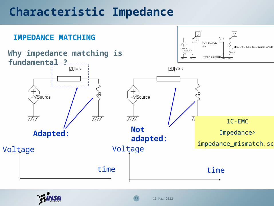
IMPEDANCE MATCHING
Adapted: Not adapted:
time
Voltage
time
Voltage
Characteristic Impedance
Why impedance matching is fundamental ?
IC-EMC
Impedance>
impedance_mismatch.sch
23 19 Apr 2023
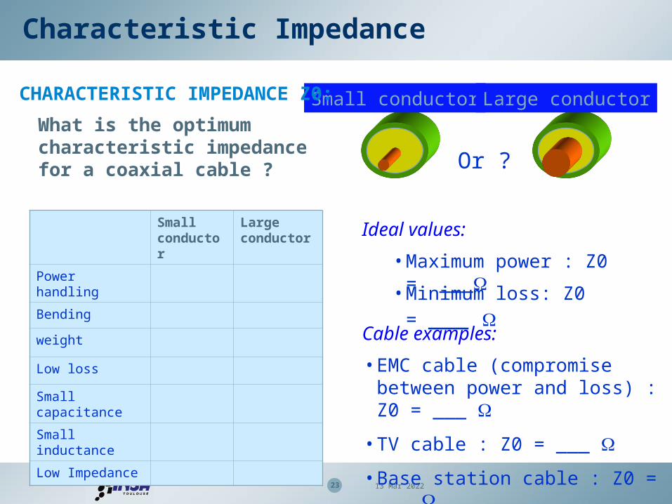
Small conductor Large conductorWhat is the optimum characteristic impedance for a coaxial cable ?
Characteristic Impedance
CHARACTERISTIC IMPEDANCE Z0:
• Maximum power : Z0 = ___
• Minimum loss: Z0 = ___
Small conductor
Large conductor
Power handling
Bending
weight
Low loss
Small capacitance
Small inductance
Low Impedance
Or ?
Ideal values:
• EMC cable (compromise between power and loss) : Z0 = ___
• TV cable : Z0 = ___
• Base station cable : Z0 = ___
Cable examples:
24 19 Apr 2023
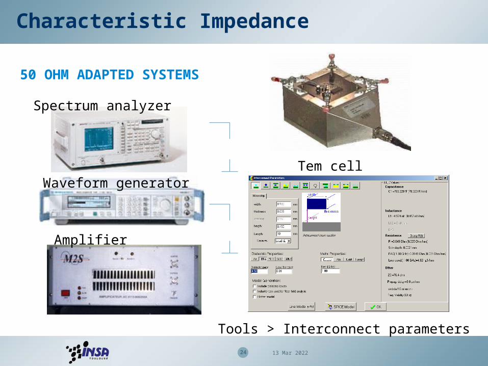
50 OHM ADAPTED SYSTEMS
Tem cell
Spectrum analyzer
Waveform generator
Amplifier
Characteristic Impedance
Tools > Interconnect parameters
25 19 Apr 2023
• Specific units used in EMC have been detailed
• The current dipole is the base for radiated emission
• The Emission Spectrum has been described
• Susceptibility Threshold, margins have been discussed
• The notion of impedance has been introduced
• Characteristic impedance of cables lead to specific values
• Discrete components used in the experimental board have
been modeled up to 1 GHz
Conclusion