ELEMENTAL ANALYSIS Nanophotonics with ... - · PDF fileELEMENTAL ANALYSIS FLUORESCENCE...
3
ELEMENTAL ANALYSIS FLUORESCENCE GRATINGS & OEM SPECTROMETERS OPTICAL COMPONENTS FORENSICS PARTICLE CHARACTERIZATION RAMAN SPECTROSCOPIC ELLIPSOMETRY SPR IMAGING Nanophotonics with Fluorescence Instruments Introduction HORIBA Jobin Yvon’s spectrofluorometers have many applications in nanophotonics research: single-walled carbon nanotubes (SWNTs), quantum dots (QDs), and organic light-emitting diodes (OLEDs). Quantum confinement affects nanomaterials’ photoluminescence: when the semiconducting nanoparticle is smaller than the bulk material’s Bohrexciton radius, the bandgap energy is inversely proportional to the nanoparticle size. Smaller nanoparticles usually have higher energy-absorbance and emission properties than larger nanoparticles of the same material. SWNTs and the NanoLog® Fig. 1 illustrates semiconducting-SWNT photoluminescence. Decreasing absorption and emission energies of individual SWNT species correlate directly with diameters from Raman spectroscopic analysis of radial breathing modes. Certain (n,m) values of semiconducting SWNTs match predicted band-gaps between valence and conductance bands. (Metallic and semimetallic SWNTs with continuous valence and conductance bands show little luminescence.) A NanoLog® (double-grating excitation monochromator, imaging emission spectrograph with a selectable grating turret, and multichannel liquid-N2-cooled InGaAs-array detector) has optimal excitation optics 1 for SWNT research or any solid sample in right-angle or front-face mirror configurations. The emission spectrometer has selectable gratings in a turret mount for rapid, easy acquisition of spectra. One grating has single-shot coverage of > 500 nm with a detector sensitive from 800–1700 nm. 2 Corrected emission spectra provide EEMs for a range of excitation wavelengths within minutes. Excitation bandpass is 0–14 nm; spectrometer slits vary from 0–16 mm with a 1200 groove/mm grating. An order-sorting filter excludes visible light from the spectrometer. Our exclusive Nanosizer® software compiles EEMs (Figs. 2a and b) to determine SWNT composition (Fig. 2c). A FL-20 Fig. 1. Semiconducting-SWNT photoluminescence absorption and emission. Conduction bands are red; valence bands are blue, electrons are yellow, holes are black. Black arrows are radiative or nonradiative transitions of e – s or holes between band-levels. V x and c x are specific valence or conductance bands. 1 Xe lamp and reference diode: 250–1000 nm; excitation monochromator’s gratings blazed at 500 nm for excitation at 333–1000 nm. 2 Grating: 150 grooves/mm, 1200 nm blaze; detector: 512 pixels × 1” [2.5 cm].
Transcript of ELEMENTAL ANALYSIS Nanophotonics with ... - · PDF fileELEMENTAL ANALYSIS FLUORESCENCE...
ELEMENTAL ANALYSIS
FLUORESCENCE
GRATINGS & OEM SPECTROMETERS OPTICAL COMPONENTS
FORENSICS
PARTICLE CHARACTERIZATION R A M A N
SPECTROSCOPIC ELLIPSOMETRY SPR IMAGING
Nanophotonics with Fluorescence Instruments
IntroductionHORIBA Jobin Yvon’s spectrofluorometers have many applications in nanophotonics research: single-walled carbon nanotubes (SWNTs), quantum dots (QDs), and organic light-emitting diodes (OLEDs). Quantum confinement affects nanomaterials’ photoluminescence: when the semiconducting nanoparticle is smaller than the bulk material’s Bohrexciton radius, the bandgap energy is inversely proportional to the nanoparticle size. Smaller nanoparticles usually have higher energy-absorbance and emission properties than larger nanoparticles of the same material.
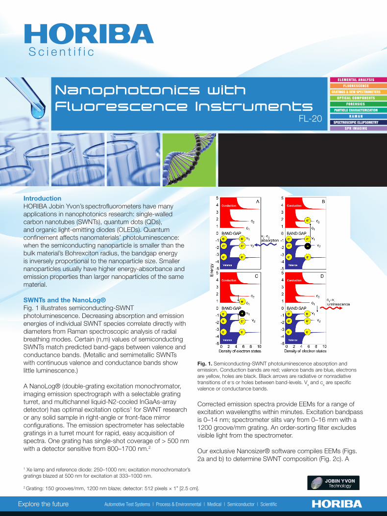
SWNTs and the NanoLog®Fig. 1 illustrates semiconducting-SWNT photoluminescence. Decreasing absorption and emission energies of individual SWNT species correlate directly with diameters from Raman spectroscopic analysis of radial breathing modes. Certain (n,m) values of semiconducting SWNTs match predicted band-gaps between valence and conductance bands. (Metallic and semimetallic SWNTs with continuous valence and conductance bands show little luminescence.)
A NanoLog® (double-grating excitation monochromator, imaging emission spectrograph with a selectable grating turret, and multichannel liquid-N2-cooled InGaAs-array detector) has optimal excitation optics1 for SWNT research or any solid sample in right-angle or front-face mirror configurations. The emission spectrometer has selectable gratings in a turret mount for rapid, easy acquisition of spectra. One grating has single-shot coverage of > 500 nm with a detector sensitive from 800–1700 nm.2
Corrected emission spectra provide EEMs for a range of excitation wavelengths within minutes. Excitation bandpass is 0–14 nm; spectrometer slits vary from 0–16 mm with a 1200 groove/mm grating. An order-sorting filter excludes visible light from the spectrometer.
Our exclusive Nanosizer® software compiles EEMs (Figs. 2a and b) to determine SWNT composition (Fig. 2c). A
FL-20
Fig. 1. Semiconducting-SWNT photoluminescence absorption and emission. Conduction bands are red; valence bands are blue, electrons are yellow, holes are black. Black arrows are radiative or nonradiative transitions of e–s or holes between band-levels. Vx and cx are specific valence or conductance bands.
1 Xe lamp and reference diode: 250–1000 nm; excitation monochromator’s gratings blazed at 500 nm for excitation at 333–1000 nm.
2 Grating: 150 grooves/mm, 1200 nm blaze; detector: 512 pixels × 1” [2.5 cm].
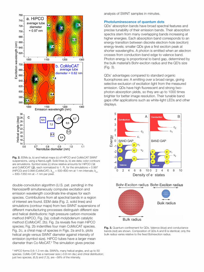
double-convolution algorithm (U.S. pat. pending) in the Nanosizer® simultaneously computes excitation and emission wavelength coordinate line-shapes for each species. Contributions from all spectral bands in a region of interest are found. EEM data (Fig. 2, solid lines) and simulations (contour maps) from two SWNT suspensions of different manufacturing processes distinguish different size and helical distributions: high pressure carbon-monoxide method (HiPCO, Fig. 2a); cobalt-molybdenum catalytic method (CoMoCAT, 2b). Fig. 2a reveals five main HiPCO species; Fig. 2b indentifies four main CoMoCAT species. Fig. 2c, a chiral map of species in Figs. 2a and b, plots helical angle versus SWNT diameter against intensity of emission (symbol size). HiPCO tubes have a larger mean diameter than Co-MoCAT.3 The simulation gives precise
analysis of SWNT samples in minutes.
Photoluminescence of quantum dotsQDs’ absorption bands have broad spectral features and precise tunability of their emission bands. Their absorption spectra stem from many overlapping bands increasing at higher energies. Each absorption band corresponds to an energy-transition between discrete electron-hole (exciton) energy-levels; smaller QDs give a first exciton peak at shorter wavelengths. A photon is emitted when an electron crosses from conduction-band edge to valence band. Photon energy is proportional to band gap, determined by the bulk material’s Bohr-exciton radius and the QD’s size (Fig. 3).
QDs’ advantages compared to standard organic fluorophores are: A emitting over a broad range, giving selective exclusion of excitation light from the measured emission. QDs have high fluorescent and strong two-photon absorption yields, so they are up to 1000 times brighter for better image resolution. Their tunable band gaps offer applications such as white-light LEDs and other displays.
Fig. 2. EEMs (a, b) and helical maps (c) of HiPCO and CoMoCAT SWNT suspensions, using a NanoLog®. Solid lines (a, b) are data; color contours are simulations. Symbol sizes (c) show relative amounts for HiPCO () and CoMOCAT (), each normalized to 1. R2 for the simulations = 0.997 (HiPCO) and 0.999 (CoMoCAT). λexc = 500–800 nm at 1 nm intervals; λem = 830–1350 nm at ~1 nm per pixel.
3 HiPCO forms 0.6–1.3 nm dia. SWNTs, many helical angles, and up to 50 species. CoMo-CAT has a narrower size (~0.8 nm dia.) and chiral distribution; just two species, (6,5) and (7,5), are ~58% of the intensity.
Fig. 3. Quantum confinement for QDs. Valence (blue) and conductance bands (red) are shown. Composition of QDs A and B is identical; only the bulk radius varies relative to the fixed Bohrexciton radius.
Most QDs are made of toxic elements (e.g., Pb, Cd, Se, and Te). Their photoluminescence may be sensitive to biological interactions, so QDs require a coating (usually a triblock copolymer), rendering the QDs nontoxic but also helping to conjugate the QDs to molecular probes, and protecting the QDs from biomolecular agents. Antibody-conjugate-imaging of these QDs may be useful to diagnose and treat cancer. Near-IR QDs may aid deeper tissue-imaging, for near-IR penetrates tissue deeper than visible light. QDs’ excited-state lifetimes (2~10 ns) increase their worth for timeresolved fluorescence instruments. Many conjugation choices and excitedstate properties of QDs make them useful for biosensors based on fluorescence resonance energy-transfer.
Photoluminescent Analysis of OLEDsBased on thin films, OLEDs offer advantages over LCDs: no back lighting, emission of light only from active pixels (lower power), higher contrast and color fidelity, brighter emission, wider viewing angles, faster temporal response, better temperature-stability, and deposition on flexible or transparent substrates.
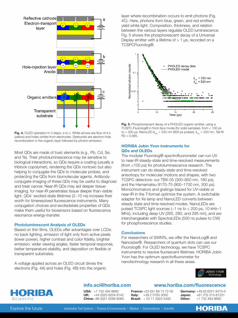
A voltage applied across an OLED circuit drives the electrons (Fig. 4A) and holes (Fig. 4B) into the organic
layer where recombination occurs to emit photons (Fig. 4C). Here, photons from blue, green, and red emitters yield white light. Composition, thickness, and relation between the various layers regulate OLED luminescence. Fig. 5 shows the phosphorescent decay of a Universal Display emitter with a lifetime of > 1 μs, recorded on a TCSPCFluorolog®.
HORIBA Jobin Yvon instruments forQDs and OLEDsThe modular Fluorolog® spectrofluorometer can run UV to near-IR steady-state and time-resolved measurements (from <100 ps) for photoluminescence research. The instrument can do steady-state and time-resolved anisotropy for molecular motions and shapes, with two TCSPC detectors: our TBX-05 (300–850 nm, 180 ps), and the Hamamatsu 9170-75 (900–1700 nm, 300 ps). Monochromators and gratings blazed for UV-visible or near-IR in the T-format optimize the system. A switchable adapter for Xe lamp and NanoLED converts between steady state and time-resolved modes. NanoLEDs are pulsed TCSPC light sources (~1 ns to ≤ 200 ps, 10 kHz–1 MHz), including deep-UV (265, 280, and 295 nm), and are interchangeable with SpectraLEDs (500 ns pulses to CW) for phosphorescence studies.
ConclusionsFor researchers of SWNTs, we offer the NanoLog® and Nanosizer®. Researchers of quantum dots can use our Fluorolog®. For OLED technology, we have TCSPC instruments to resolve fluorescent lifetimes. HORIBA JobinYvon has the optimum spectrofluorometer for nanotechnology research in all these areas.
Fig. 4. OLED operation in 3 steps, a to c. White arrows are flow of e–s (yellow) and holes (white) from electrodes. Starbursts are electron-hole recombination in the organic layer followed by photon-emission.
Fig. 5. Phosphorescent decay of a PHOLED organic emitter, using a TCSPC-Fluorolog® in front-face mode (for solid samples), from < 100 ps to > 200 μs. NanoLED λexc = 335 nm (800 ps pulses); λem = 520 nm. Tail-fit R2 = 0.995.
[email protected] www.horiba.com/fl uorescenceUSA: +1 732 494 8660 France: +33 (0)1 69 74 72 00 Germany: +49 (0) 6251 8475-0UK: +44 (0)20 8204 8142 Italy: +39 2 5760 3050 Japan: +81 (75) 313-81231China: +86 (0)21 6289 6060 Brazil: + 55 11 2923 5400 Other: +1 732 494 8660