Electronics West 2009 - LA/OC SMTA Chapter Home Page · Voiding and head in pillow defects Pad...
6
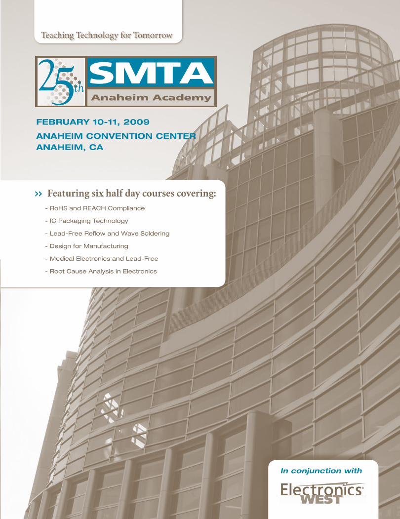
FEBRUARY 10-11, 2009 ANAHEIM CONVENTION CENTER ANAHEIM, CA >> Featuring six half day courses covering: - RoHS and REACH Compliance - IC Packaging Technology - Lead-Free Reflow and Wave Soldering - Design for Manufacturing - Medical Electronics and Lead-Free - Root Cause Analysis in Electronics In conjunction with Teaching Technology for Tomorrow
Transcript of Electronics West 2009 - LA/OC SMTA Chapter Home Page · Voiding and head in pillow defects Pad...
>> Featuring six half day courses covering:
- RoHS and REACH Compliance
- IC Packaging Technology
- Lead-Free Reflow and Wave Soldering
- Design for Manufacturing
- Medical Electronics and Lead-Free
- Root Cause Analysis in Electronics
February 10-11, 2009
anaheim Convention Center anaheim, Ca
>> Featuring six half day courses covering: - RoHS and REACH Compliance
- IC Packaging Technology
- Lead-Free Reflow and Wave Soldering
- Design for Manufacturing
- Medical Electronics and Lead-Free
- Root Cause Analysis in Electronics
In conjunction with
Teaching Technology for Tomorrow
1. Registration Information
r Dr. r Mr. r Ms. SMTA Member #: ________________________________________________________________________________
Name _________________________________________________ Job Title ____________________________________________________
Company ________________________________________________ MS _______________________________________________________
Address ____________________________________________________________________________________________________________
City ____________________________________ State/Province _____________ Zip ______________ Country _______________________
Phone ____________________________________ Fax ____________________________________ E-Mail ___________________________
2. How to Register
Register Online! By fax with By phone with By mail with www.smta.org credit card credit card payment to SMTA 952-926-1819 952-920-7682 5200 Willson Road, Suite 215 Edina, MN 55424-1316
3. Registration Fee (US$$) Register before January 8 and save 10%
Academy Courses Anaheim, CA
Half Day Courses Member Non-Memberr T1 $250 $350r T2 $250 $350r T3 $250 $350r T4 $250 $350r T5 $250 $350r T6 $250 $350
4. Payment Options
Total Amount Due __________________________________________
r Check enclosed (US$$) r Purchase order # ___________________
r MC r VISA r AMEX
Credit Card # ______________________________________________
Expiration Date ____________________________________________
Cardholder’s Name __________________________________________
5. Registration Registration
Pre-Registration is strongly recommended. There will be no guarantee of space or materials for on-site registrants.
Four Registrations for the Price of Three
If four employees from the SAME company each register for a course, the fourth registrant is free!
Registration Fee
The registration fee for the Academy courses includes course materials and coffee breaks.
Cancellation
Registration fees will be refunded (less a $50 processing fee), if written notice is postmarked two weeks prior to program date.
No Shows
Registration fee will not be refunded in order to cover expenses incurred.
| register beFore january 8 and save!SMTA Anaheim Academy Registration
All Academy Attendees who are Non-Members will receive a one-year SMTA Individual Membership. Current individual members will receive a one-year membership renewal. (One renewal allowed per year.)
For more information on the SMTA Anaheim program, please contact Melissa Serres Marx at [email protected] or 952-920-7682 or visit the SMTA Web site at www.smta.org/education/academy/academy.cfm.
Hotel Information
Hotel information is available at www.electronicswestshow.com. Click on the “Travel” tab at the top of the page and scroll down to hotels for a complete listing of options and booking information.
SMTA5200 Willson Road, Ste. 215Edina, MN 55424-1343
Presorted Standard
U.S. Postage PAID
Minneapolis, MNPermit No. 28788
Teaching Technology for Tomorrow
February 10-11, 2009
anaheim Convention Center anaheim, Ca
The SMTA is proud to co-locate the SMTA Anaheim Academy with Electronics West 2009.
Electronics West 2009 The West Coast’s Electronics Manufacturing Marketplace
You will find everything you need, including: THE latest advances in electronics manufacturing including; adhesives and solder, contract services, electronic
components, PCB production equipment, subassemblies, software,... and more.
THE leading suppliers who know your industry...suppliers with years of experience in every market segment, including Aerospace/Aviation/Military, Automotive, Computers, Consumer Products/Appliances, Industrial Equipment, Information Technology, Medical Equipment and Devices, Motors and Generators, Office Equipment, Test/Scientific/Instrumentation, Telecommunications, and many more.
Technical experts in every booth who are ready to discuss your product specifications and requirements. Match their expertise and capabilities with your needs.
Business-building opportunities to explore supplier alliances, technology licensing, partnerships, and joint ventures.
Six industry-relevant co-located shows: Your Electronics West badge also provides free admission to MD&M West, WestPack, ATX West, Pacific Design & Manufacturing, PLASTEC West Pavilion, and Green Manufacturing Expo.
For more information about Electronics West 2009 and the other co-located shows, or to register for FREE expo hall admission, please visit ElectronicsWestShow.com.

4
SMTA Anaheim Academy Courses | February 10-11, 2009
T1: Creating a RoHS and REACH Compliance System Rob Rowland, RadiSys Corporation
Tuesday, February 10 8:30am - 12:00pm
What You Will LearnThe European RoHS (Restrictions on Hazardous Substances) directive was just the beginning. RoHS has become a global initiative and other countries, such as China, are jumping on the bandwagon. There are currently six restricted substances (lead, mercury, cadmium, hexavalent chromium, polybrominated biphenyls and polybrominated diphenyl ethers) and 29 exemptions. Pb-free gets most of the publicity, but the entire RoHS restricted substance list must be dealt with to achieve RoHS compliance. The REACH (Registration, Evaluation, Authorization and Restriction of Chemicals) directive and substances of very high concern are also starting to impact the industry. This workshop will cover key elements of the European and China RoHS directives including the restricted substance list, concentration values, technical issues and challenges, exemptions, enforcement, labeling, data collection, verifiable objective evidence and material declarations. It will also cover REACH and the substances of very high concern list.
Topics Covered European RoHS Directive/ China RoHS Directives REACH Directive Substances of very high concern EU and China RoHS comparison Definitions of RoHS compliance RoHS restricted substance list Maximum concentration value Homogenous material level JIG (Joint Industry Group) list Product groups affected by RoHS European RoHS exemptions Pb exemption interpretation China RoHS labeling options & disclosure table Creating a RoHS compliance strategy Collecting RoHS compliant information RoHS compliance and enforcement Verifiable Objective Evidence (VOE) RoHS test methods and equipment Software tools for RoHS compliance IPC-175X material declaration format IPC-1752 material declaration classes Lead-free marking standards What’s next for RoHS and REACH?
Who Should AttendThis workshop is intended for individuals who are involved in environmental compliance activities such as RoHS and REACH. The information presented in this workshop will be beneficial to anyone involved with RoHS and REACH compliance including engineers, buyers and managers.
T2: IC Packaging Technology Evolution and Future Directions Joseph Fjelstad, Verdant Electronics
Tuesday, February 10 8:30am - 12:00pm
What You Will LearnIC packaging technology was at one time considered an unfortunate necessity. However, over the course of the last decade IC packaging has risen greatly in importance. Today, the IC package in all of its numerous manifestations is the gate keeper of much of the cost and performance of electronic systems. This highly competitive sector of the electronics manufacturing infrastructure is also one of the most innovative and enabling. IC packaging has made possible the continuous reduction in cell phone size even as features dramatically increased. This workshop will trace the history of IC packaging technology from its simple beginnings to today’s complex 3D structures that are extending the boundaries of the technology to new realms.
Topics Covered IC assembly basics IC package types and structures Chip scale and wafer level packaging 3D assemblies Testing requirements Speculative crystal ball look into the future
Who Should AttendThis course is broad in scope on the topic of IC packaging and thus of potential interest to a wide range of prospective participants of wide ranging experience levels including: circuit designers and design engineers, product and project engineers and managers, quality and purchasing professionals wishing to expand their understanding of IC packaging technology and is suitable as well for those just entering the electronics manufacturing industry.
T3: Pb-free Reflow and Wave Soldering Guidelines Rob Rowland, RadiSys Corporation
Tuesday, February 10 1:30pm – 5:00pm
What You Will LearnSurface mount and through hole soldering processes are challenging and Pb-free soldering adds another level of complexity. After more than two years of Pb-free volume production how are things going? This workshop identifies and examines the critical process parameters associated with the transition to Pb-free reflow and wave soldering. Participants will examine these processes from multiple viewpoints including components, substrates, flux, solder alloys and the equipment. The goal is to successfully merge these topics into robust Pb-free reflow and wave soldering processes. Each topic uses a “what changed” approach which explains the differences between
SnPb and Pb-free soldering plus the basic theory of operation, recommended operating parameters, monitoring and measuring concepts, and related industry standards.
Four critical factors – substrates, components, flux and solder – influence soldering profiles. This workshop will cover these topics plus time and temperature profiles, zone and preheat parameters, conveyor speed calculation, profiling methods, profiling equipment and mixed alloy (Sn/Pb and Pb-free) soldering. The reliability of Pb-free substrates and solder joints are key concerns; reliability testing and failure analysis for both of these topics will be covered. In particular, substrate (PCB) reliability has been hit hard by the transition to Pb-free. Another interesting Pb-free topic, tin whiskers, will also be covered in detail. A list of reflow soldering, wave soldering and inspection equipment suppliers is included.
Topics Covered Steps to creating reflow and wave profiles Component peak temperature Component ramp up and ramp down rates Component surface finish Tin whisker theory and risk Moisture sensitive devices PCB glass transition temperature PCB coefficient of thermal expansion PCB material decomposition temperature PCB time to delamination PCB surface finish Flux activation temperature and time Rosin, water soluble and no-clean flux Flux classification per J-STD-004 SnPb and Pb-free solder alloy options Pb-free solder joint appearance SnPb and Pb-free soldering scenarios Mixed alloy (Sn/Pb and Pb-free) soldering Pb-Free BGAs with SnPb solder Solder paste basics per J-STD-005 Stencil apertures and wetting after reflow Reflow and wave soldering phases Reflow and wave soldering profiles Conveyor speed calculation Reflow oven zone settings Pb-free solder pots Pb-free substrate (PCB) reliability Pb-free solder joint reliability Voiding and head in pillow defects Pad cratering and CAF defects Related industry standards
Who Should AttendThis workshop is intended for individuals who are involved in the transition to Pb-free reflow and wave soldering. The information presented in this workshop will be beneficial to anyone involved with Pb-free reflow and wave soldering including engineers, operators and managers. Some basic knowledge of surface mount technology is helpful but not essential.
T4: Design for Manufacturing: Elements in Today’s Electronic Designs that Can No Longer be Ignored Dale Lee, Plexus Corporation
Wednesday, February 11 8:30am- 12:00pm
What You Will LearnComponent packaging technology continues to decrease in size (length, width, thickness), interconnection density per unit area is increasing (thinner PCB’s, smaller lines & spaces), functional performance is increasing (thermal, mechanical, electrical) at the same time as assembly processes are changing to lead-free assembly and other legislated requirements.
Due to these evolutionary changes in technology, many elements in the product design, PCB fabrication and assembly process that used to be ignored can no longer be ignored. This course will provide insight and highlight examples of several finer point DFX elements within product design process (PCB and assembly), manufacturing tooling design, SMT and PTH assembly, cleaning, SMT and PTH rework, and inspection/test opportunities that may impact process deployment and yield improvement.
Who Should AttendThis event is ideally suited to new and experienced PCB/PCBA designers, manufacturing and process engineers, quality and inspection staff, production operators and any members of staff tasked with looking at yield monitoring and process improvements on printing and reflow. Managers and supervisors would also benefit from a fuller understanding of the issues currently being experienced in industry.
T5: Pb-Free and Medical Applications Craig Hillman, Ph.D., DfR Solutions
Wednesday, February 11 8:30am - 12:00pm
What You Will LearnThe day of reckoning regarding Pb-free continues to come closer for most medical OEMs. While there is a wide range of medical applications, with a diversity so great that the idea that they have a unique set of requirements can be called into question, the need and approach to Pb-free does have some general similarities. In this seminar, specific case studies will be used to provide guidance and understanding on how the medical industry is dealing with Pb-free and identify the organic evolution of a series of industry best practices. A specific focus will be on quality and reliability assurance and how these activities are in play for devices that monitor, treat, and control medical situations.
For more information visit us online at www.smta.org
Topics Covered Scrubbing of bill of materials (BOM) for RoHS compliance and
compatibility Tin whisker risk assessment and mitigation Selecting and qualifying printed board materials Developing controlled Pb-free processes Product qualification testing and acceptance
Course Outline Introduction Environmental Legislation Worldwide (RoHS, REACH, ELV,
etc.) Case Study: Devices for Emergency Treatment
• Specific requirements and limitations (complexity, volume of production, use environment)
• Potential challenges • Field issues • Identified solutions
Case Study: Complex Systems for Medical Treatment • Specific requirements and limitations
(complexity, volume of production, use environment) • Potential challenges • Field issues • Identified solutions
Case Study: Implantable Devices • Specific requirements and limitations
(complexity, volume of production, use environment) • Potential challenges • Field issues • Identified solutions
Conclusion
T6: Understanding Failure and Root Cause Analysis in Electronics Craig Hillman, Ph.D., DfR Solutions
Wednesday, February 11 1:30pm - 5:00pm
What You Will LearnIncreasing needs for performance, low cost, and a constant turnover in the electronics industry makes improving functionality a constant topic of interest. However, restrictions on machine performance (is your computer much better than the one two years ago?) and cost (how many more companies can move to China?) have made quality/reliability a critical differentiator in today’s crowded marketplace. How to ensure optimum quality/reliability of your product? It all starts with root-cause analysis, which is the fundamental exercise in understanding how electronic products can and will fail.
This course will provide an in-depth understanding of the common mechanisms that initiate failure in electronics and provides a comprehensive review of the tools and techniques to identify those mechanisms. Mechanisms are addressed based upon the packaging level in which they are affiliated, including die, component packaging, discrete components, printed circuit board,
interconnect, and separable connector. A physics of failure (PoF) based approach to the mechanisms are taken, with an outline of drivers of these mechanisms, including defect-driven, overstress, and wearout, and how an understanding of these stress-strength interactions can provide guidance on the appropriate corrective and preventative action.
Once the participants have an understanding of failure mechanism behavior, a systematic process of proceeding with a root-cause analysis is provided. An overview of current and effective strategic and physical tools and techniques are provided within progressing stages of least-destructive to more destructive analysis and evaluation. A wide variety of case studies, including red phosphorus in epoxy encapsulants and bulging electrolytic capacitors, are provided as valuable teaching examples.
Topics Covered Failure Mechanisms
• On-Die • Packaging (Wirebonds, Die Attach, Epoxy Encapsulant) • Discrete Components (Capacitors, Resistors,
Magnetic components, etc.) • Interconnects • Printed Circuit Boards
Management • Failure Analysis Management and Reporting • Documentation (5-Phase, 8-D)
Tools • X-ray Microscopy • Acoustic Microscopy • Electrical Characterization • Visual Inspection • Thermal Imaging • Mechanism identification (Fishbone, Stress-Strength,
Fault Tree) • Cross-Sectioning • Decapsulation • Optical Microscopy • Electron Microscopy • Ion Chromatography • Surface Analysis Techniques (FTIR, EDS, XRF, etc.) • Material Analysis Techniques (DSC, TMA, TGA, etc.) • Mechanical Analysis Techniques (Microtester, Bend
Testing, etc.)
Who Should AttendThis course is intended as an introductory to intermediate level course for board-level designers, component engineers, quality engineers, reliability engineers, and their managers.
________________________________________________
Visit the SMTA in Booth #242 on the Electronics West show floor________________________________________________

>> Featuring six half day courses covering:
- RoHS and REACH Compliance
- IC Packaging Technology
- Lead-Free Reflow and Wave Soldering
- Design for Manufacturing
- Medical Electronics and Lead-Free
- Root Cause Analysis in Electronics
February 10-11, 2009
anaheim Convention Center anaheim, Ca
>> Featuring six half day courses covering: - RoHS and REACH Compliance
- IC Packaging Technology
- Lead-Free Reflow and Wave Soldering
- Design for Manufacturing
- Medical Electronics and Lead-Free
- Root Cause Analysis in Electronics
In conjunction with
Teaching Technology for Tomorrow
1. Registration Information
r Dr. r Mr. r Ms. SMTA Member #: ________________________________________________________________________________
Name _________________________________________________ Job Title ____________________________________________________
Company ________________________________________________ MS _______________________________________________________
Address ____________________________________________________________________________________________________________
City ____________________________________ State/Province _____________ Zip ______________ Country _______________________
Phone ____________________________________ Fax ____________________________________ E-Mail ___________________________
2. How to Register
Register Online! By fax with By phone with By mail with www.smta.org credit card credit card payment to SMTA 952-926-1819 952-920-7682 5200 Willson Road, Suite 215 Edina, MN 55424-1316
3. Registration Fee (US$$) Register before January 8 and save 10%
Academy Courses Anaheim, CA
Half Day Courses Member Non-Memberr T1 $250 $350r T2 $250 $350r T3 $250 $350r T4 $250 $350r T5 $250 $350r T6 $250 $350
4. Payment Options
Total Amount Due __________________________________________
r Check enclosed (US$$) r Purchase order # ___________________
r MC r VISA r AMEX
Credit Card # ______________________________________________
Expiration Date ____________________________________________
Cardholder’s Name __________________________________________
5. Registration Registration
Pre-Registration is strongly recommended. There will be no guarantee of space or materials for on-site registrants.
Four Registrations for the Price of Three
If four employees from the SAME company each register for a course, the fourth registrant is free!
Registration Fee
The registration fee for the Academy courses includes course materials and coffee breaks.
Cancellation
Registration fees will be refunded (less a $50 processing fee), if written notice is postmarked two weeks prior to program date.
No Shows
Registration fee will not be refunded in order to cover expenses incurred.
| register beFore january 8 and save!SMTA Anaheim Academy Registration
All Academy Attendees who are Non-Members will receive a one-year SMTA Individual Membership. Current individual members will receive a one-year membership renewal. (One renewal allowed per year.)
For more information on the SMTA Anaheim program, please contact Melissa Serres Marx at [email protected] or 952-920-7682 or visit the SMTA Web site at www.smta.org/education/academy/academy.cfm.
Hotel Information
Hotel information is available at www.electronicswestshow.com. Click on the “Travel” tab at the top of the page and scroll down to hotels for a complete listing of options and booking information.
SMTA5200 Willson Road, Ste. 215Edina, MN 55424-1343
Presorted Standard
U.S. Postage PAID
Minneapolis, MNPermit No. 28788
Teaching Technology for Tomorrow
February 10-11, 2009
anaheim Convention Center anaheim, Ca
The SMTA is proud to co-locate the SMTA Anaheim Academy with Electronics West 2009.
Electronics West 2009 The West Coast’s Electronics Manufacturing Marketplace
You will find everything you need, including: THE latest advances in electronics manufacturing including; adhesives and solder, contract services, electronic
components, PCB production equipment, subassemblies, software,... and more.
THE leading suppliers who know your industry...suppliers with years of experience in every market segment, including Aerospace/Aviation/Military, Automotive, Computers, Consumer Products/Appliances, Industrial Equipment, Information Technology, Medical Equipment and Devices, Motors and Generators, Office Equipment, Test/Scientific/Instrumentation, Telecommunications, and many more.
Technical experts in every booth who are ready to discuss your product specifications and requirements. Match their expertise and capabilities with your needs.
Business-building opportunities to explore supplier alliances, technology licensing, partnerships, and joint ventures.
Six industry-relevant co-located shows: Your Electronics West badge also provides free admission to MD&M West, WestPack, ATX West, Pacific Design & Manufacturing, PLASTEC West Pavilion, and Green Manufacturing Expo.
For more information about Electronics West 2009 and the other co-located shows, or to register for FREE expo hall admission, please visit ElectronicsWestShow.com.